A New Chip Supercycle? TSMC’s February Signals the AI Era Has Arrived
A New Chip Supercycle? TSMC’s February Signals the AI Era Has Arrived
- Source: SemiVision
- Author: SEMIVISION
- Published: 2026-03-12T09:12:25+08:00
- URL: https://tspasemiconductor.substack.com/p/a-new-chip-supercycle-tsmcs-february (1) A New Chip Supercycle? TSMC’s February Signals the AI Era Has Arrived


A New Chip Supercycle? TSMC’s February Signals the AI Era Has Arrived
Original Article By SemiVision Research [Reading time: 10 mins]

Mar 12, 2026
∙ Paid
TSMC’s Strongest February Ever: Why AI Demand, Faster Capacity Expansion, and Advanced Packaging Are Rewriting the Semiconductor Cycle
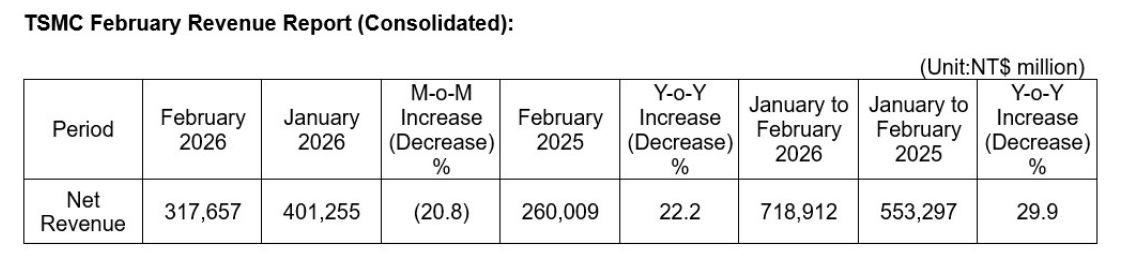
TSMC has once again reminded the market why it sits at the center of the global semiconductor industry. According to the news clippings provided, the company posted its strongest February revenue on record, reaching NT$317.657 billion, down 20.8% month over month but up 22.2% year over year. More importantly, market observers believe March revenue could challenge NT$400 billion again, reinforcing the idea that TSMC is no longer moving in lockstep with the old consumer-electronics cycle.
That matters far beyond one month of revenue. It signals a structural shift in semiconductors: the industry is being increasingly driven not just by smartphones, PCs, and seasonal launches, but by AI infrastructure, high-performance computing (HPC), and the massive buildout of advanced packaging capacity.
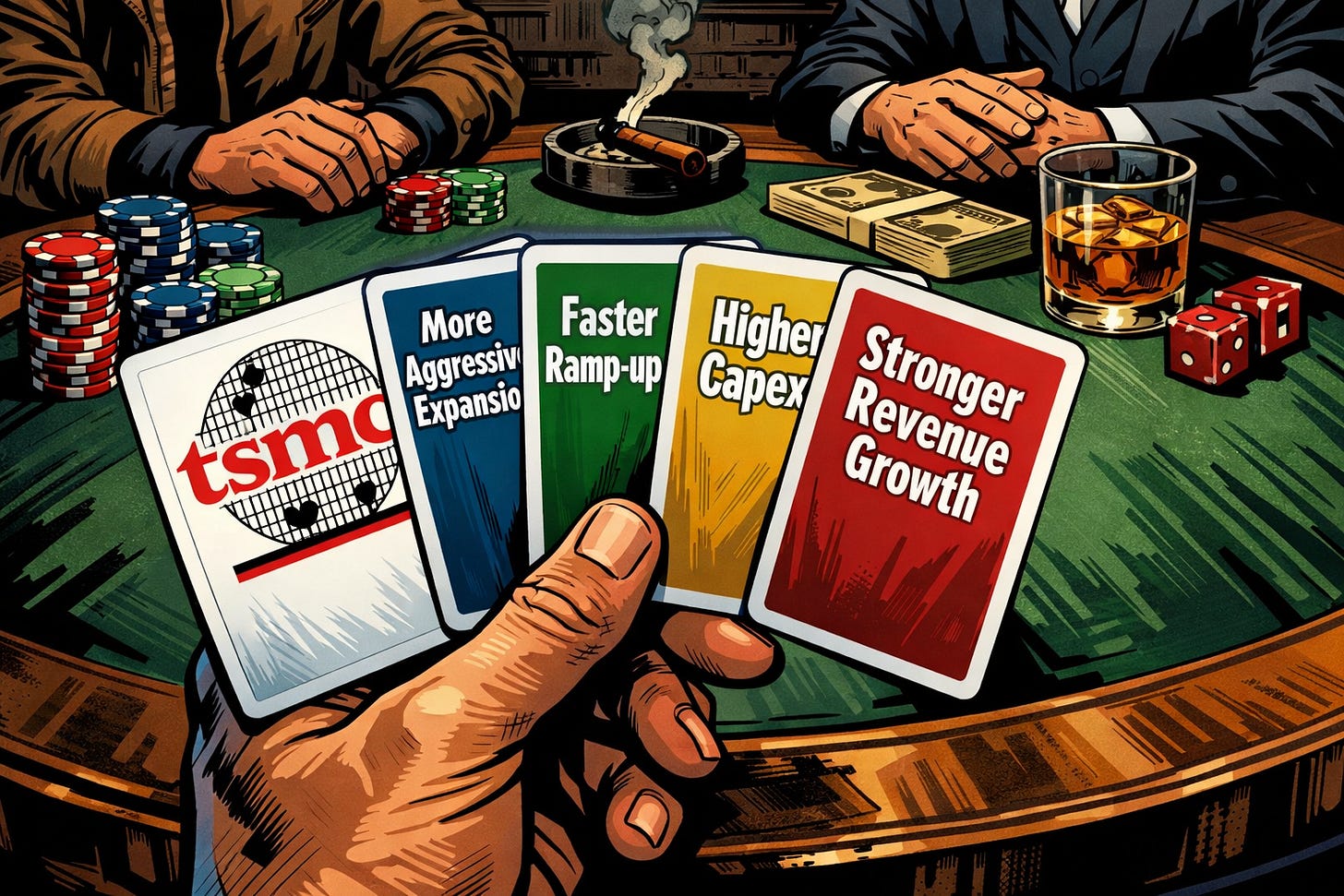
The second clipping goes even further. It highlights what Morgan Stanley calls TSMC’s “four major positives”: more aggressive capacity expansion, faster ramp-up speed, higher capital expenditure, and strong revenue growth. The report argues that these changes justify a higher valuation and a more bullish long-term view.
Taken together, these reports are not just about one company’s earnings momentum. They offer a window into the next phase of the semiconductor industry—one in which process leadership, advanced packaging, and execution speed are becoming just as important as transistor scaling itself.

1月16日
A strong February is not just a strong February
On the surface, a month-over-month decline of more than 20% may seem weak. But in semiconductors, February often has fewer working days, and Taiwan-based manufacturers are usually affected by the Lunar New Year holiday pattern. What stands out here is that, despite seasonal disruption, TSMC still posted the highest February revenue in its history.
That tells us two things.
First, underlying demand remains extremely strong. Even when calendar effects weigh on shipments, the baseline revenue level is much higher than it used to be. Second, the revenue mix is changing. NVIDIA has become TSMC’s largest customer, which is highly significant. NVIDIA’s AI GPUs, along with accelerators from AMD and custom chips from cloud service providers, are tied to a different spending pattern than smartphones.

2月26日
Traditional semiconductor demand tends to be cyclical and product-season driven. Smartphone launches, notebook refreshes, and holiday retail sales create peaks and troughs. AI infrastructure demand works differently. Hyperscalers and sovereign AI projects buy based on compute deployment schedules, cluster expansion plans, power availability, and data center construction timelines. These are larger, longer-cycle investments, but when they happen, the order sizes can be enormous.
This is why TSMC’s February result is important. It suggests that AI-related demand is offsetting more of the usual seasonal weakness, making the company’s revenue profile more resilient.
Why AI changes the foundry business model
For decades, foundries like TSMC were essentially manufacturing partners for fabless chip companies. That remains true, but AI has changed the economics of the relationship.
In the AI era, winning at the foundry level is no longer only about making the smallest transistors. It is about delivering an entire performance stack:
Leading-edge logic nodes
Advanced packaging
High-bandwidth memory integration
Power delivery efficiency
Yield management at very large die sizes
Fast time-to-volume
Modern AI chips are extremely complex. A cutting-edge accelerator is no longer just a monolithic chip. It is often a system-level package, combining a large compute die or chiplets with HBM stacks and advanced interconnect structures. That means the foundry is no longer just fabricating transistors; it is helping enable the entire architecture.
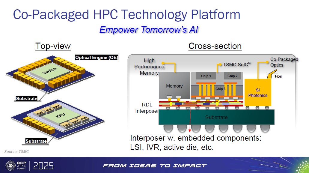
This is one reason TSMC has become so central to the AI supply chain. Its advantage comes from the combination of:
Leading process technologysuch as 5nm, 3nm, and beyond
Advanced packaging capabilitiessuch as CoWoS
Manufacturing scale and yield discipline
Tight ecosystem coordinationwith GPU, ASIC, and memory players
In other words, TSMC is not just selling wafers. It is increasingly selling integration capability.

1月31日
Understanding CoWoS: the packaging bottleneck that became a growth engine
One of the most important semiconductor concepts behind these reports is CoWoS, short for Chip-on-Wafer-on-Substrate. This is TSMC’s flagship advanced packaging technology and one of the biggest beneficiaries of AI demand.

Why does CoWoS matter so much?
Because AI accelerators need extremely high memory bandwidth. Standard packaged chips cannot easily provide enough bandwidth between the compute die and memory. That is where HBM, or High Bandwidth Memory, comes in. HBM uses vertically stacked DRAM dies and connects them to the logic processor through a very wide interface, often via a silicon interposer inside an advanced package.
CoWoS enables this architecture. It allows a large logic die and multiple HBM stacks to be integrated in a single high-performance package. This shortens electrical path lengths, improves bandwidth, and reduces power per bit transferred compared with more conventional approaches.
In AI systems, this is essential. Training and inference workloads are often memory-bandwidth constrained. No matter how powerful the compute engine is, it becomes inefficient if it cannot be fed data fast enough. CoWoS is one of the technologies that solves that bottleneck.

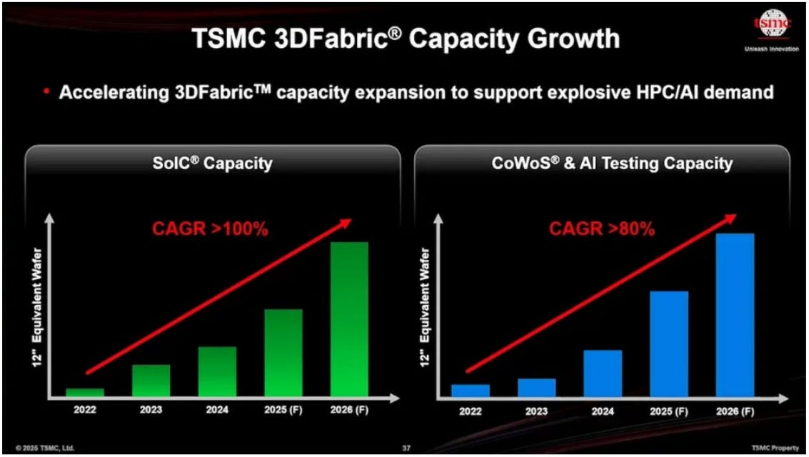
TSMC’s 2027-end CoWoS monthly capacity forecast may be increased from 155,000 wafers to 170,000 wafers. That is a striking number. It suggests that advanced packaging is no longer a side business attached to front-end manufacturing. It is becoming a major industrial pillar in its own right.

2025年5月31日
Faster ramp-up matters as much as node leadership
TSMC has shortened:
new-node production rampfrom16 months to 12 months
cleanroom constructionfrom18 months to 15 months
equipment move-infrom8 months to 6 months
These improvements may sound operational, but they are strategically important.
In semiconductors, time is money in the most literal sense. A new fab can cost tens of billions of dollars. If a company can shorten the time between capital expenditure and revenue generation, it improves return on invested capital, reduces bottlenecks, and responds faster to demand surges.
This becomes even more critical in AI, where customers do not simply want the best chip—they want it now. Hyperscalers are engaged in a race for compute capacity. Delays in manufacturing or packaging can delay entire data center deployments. A foundry that can compress the ramp timeline gains a competitive advantage, even if its process technology is only marginally ahead.
Execution speed is particularly powerful when combined with ecosystem lock-in. If TSMC can ramp advanced nodes and advanced packaging faster than rivals, its customers can launch faster, scale faster, and monetize AI infrastructure sooner. That strengthens the foundry-customer relationship and makes switching harder.
2025年9月25日
Higher capital expenditure is a feature, not a warning sign
Many investors are trained to worry when capital expenditure rises too fast. In mature industries, that can signal overexpansion. But in semiconductors—especially today—the story is more nuanced.
The second clipping says Morgan Stanley raised its TSMC capex forecast to:
US$65 billion in 2027, up from US$59 billion
US$70 billion in 2028, up from US$60 billion
Those are huge numbers. But the key question is not whether capex is high. The real question is whether the capex is being deployed into areas with strong structural demand and high returns.
At the moment, the answer appears to be yes.
AI accelerators require leading-edge wafers, advanced packaging, sophisticated substrates, and enormous backend support. Demand is not being pulled by one single application; it is being pushed by an entire industry transition toward generative AI, agentic systems, large inference clusters, and AI-native data center architecture.
Higher capex in this context reflects:
capacity needed for 3nm and beyond
packaging expansion for CoWoS and related platforms
geographic diversification
support for customers with increasingly complex designs
This is important semiconductor knowledge:not all capacity is equal. A fab for commodity trailing-edge chips is very different from capacity built around AI-class compute and packaging. What TSMC is doing is not generic expansion. It is highly targeted expansion in the most valuable segments of the market.

2月23日
Why TSMC’s growth says something about the whole industry
TSMC is often described as a proxy for the semiconductor sector, but that is only partially true. It is better understood as a proxy for the most advanced and strategically important layers of the semiconductor stack.
When TSMC reports strong results, it often indicates strength in:
AI accelerators
server CPUs
networking ASICs
advanced smartphone SoCs
custom silicon for cloud providers
advanced packaging demand
HBM-related ecosystem activity
This does not automatically mean the entire chip market is booming. Mature-node chips for industrial, automotive, or consumer applications can follow different cycles. Memory can behave differently from logic. Analog and discrete power devices can face their own supply-demand dynamics.
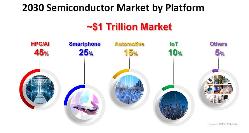
But TSMC’s recent momentum tells us that the high-end compute and packaging segment remains exceptionally strong. In today’s market, that segment exerts outsized influence because it drives the most aggressive investment and the highest ASPs.
TSMC’s strong revenue growth is making the company less dependent on consumer seasonality. That is a major structural change. Historically, smartphone cycles heavily influenced semiconductor sentiment. Today, AI infrastructure spending is emerging as a parallel and perhaps more powerful demand engine.
The broader semiconductor knowledge behind the story
To fully understand why the market is so focused on TSMC, it helps to review a few core semiconductor principles.
Leading-edge nodes still matter
Even though packaging is becoming more important, transistor scaling remains fundamental. Smaller nodes generally provide higher transistor density, better performance, lower power, or some combination of the three. AI chips need all of these. The more compute you can fit into a given power envelope, the more economically attractive the system becomes.
Yield is everything
At advanced nodes, very large dies are difficult and expensive to manufacture. A few percentage points of yield improvement can have huge effects on gross margin and customer supply. TSMC’s reputation for manufacturing discipline is one reason top customers rely on it.
Packaging is now part of performance
In older generations, packaging was mainly about protection and connectivity. In modern AI systems, packaging directly affects bandwidth, power, latency, thermal management, and system size. This is why CoWoS and related technologies matter so much.
Semiconductor leadership is ecosystem leadership
A chip is no longer just a chip. It depends on EDA tools, IP blocks, substrates, advanced materials, thermal solutions, HBM supply, server design, and software enablement. TSMC’s position is strong because it operates within an ecosystem that can support these complex products at scale.
Capacity planning is strategic
Semiconductors cannot be scaled overnight. New fabs, cleanrooms, and packaging lines take time, capital, and highly specialized equipment. Companies that anticipate demand correctly can dominate an upcycle. Companies that move too slowly can miss years of growth.
Why the market is assigning a higher target price
TSMC’s bullish case around four core drivers:
More aggressive expansion
Faster ramp-up
Higher capex
Stronger revenue growth.
These support a higher valuation because they imply that TSMC is not merely enjoying a cyclical rebound. Instead, it may be capturing a larger and more durable share of the value created by the AI buildout.
The logic is straightforward.
If TSMC can:
add more advanced-node and packaging capacity,
shorten the time to production,
support stronger long-term revenue growth,
and remain the preferred manufacturing partner for the most valuable AI chips,
then its earnings power several years from now could be materially higher than previous models assumed.
That is why analysts are willing to move price targets higher. They are effectively saying that the addressable opportunity has expanded, and TSMC’s execution is improving at the same time.
2025年7月16日
SemiVision thoughts: TSMC is becoming the infrastructure layer of the AI age
The most important takeaway from these clippings is not simply that TSMC had a strong month or that analysts are bullish. It is that TSMC is increasingly functioning as core infrastructure for the AI era.
In the past, semiconductor leadership was often framed as a node race: who had the smallest transistor, the best PPA, the most advanced lithography. That still matters. But the industry is entering a broader competitive paradigm.
Today, leadership means being able to deliver:
advanced logic
advanced packaging
rapid ramp-up
strong yields
massive scale
supply-chain coordination
long-term customer trust
TSMC appears to be strengthening across all of these dimensions.
Its record February revenue suggests the AI demand engine remains powerful. The possibility of March revenue challenging NT$400 billion shows that momentum is not fading. The discussion around CoWoS capacity, fab expansion, and accelerated construction timelines shows that the company is not standing still—it is building for the next wave.
For the semiconductor industry, this is a profound signal. The winners of the next decade may not be the companies with the best product slide decks or the loudest AI narratives. They will be the companies that can actually convert technological ambition into manufacturable, scalable, and profitable silicon systems.
Right now, TSMC looks more and more like the company doing exactly that.

2025年9月21日

2025年6月27日

2025年6月25日

2025年6月12日

2025年6月2日


PreviousNext
TopLatestDiscussions








See all