OFC 2026 Outlook: AI Data Center Optical Interconnect Trends from Pluggable Optics and LPO to CPO and MicroLED
OFC 2026 Outlook: AI Data Center Optical Interconnect Trends from Pluggable Optics and LPO to CPO and MicroLED
- Source: SemiVision
- Author: SEMIVISION
- Published: 2026-03-10T10:45:43+08:00
- URL: https://tspasemiconductor.substack.com/p/ofc-2026-outlook-ai-data-center-optical (1) OFC 2026 Outlook: AI Data Center Optical Interconnect Trends from Pluggable Optics and LPO to CPO and MicroLED


OFC 2026 Outlook: AI Data Center Optical Interconnect Trends from Pluggable Optics and LPO to CPO and MicroLED
Original Article By SemiVision Research [Reading time: 15 mins]

Mar 10, 2026
∙ Paid
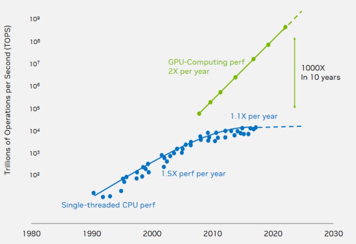
Why AI is forcing an optical revolution: “Huang’s Law” meets the I/O wall

As generative AI models scale rapidly, the primary data-center bottleneck is shifting from transistor performance to interconnect bandwidth and latency. Jensen Huang’s widely cited “Huang’s Law” framing argues that compute can compound through process scaling + 3D packaging/vertical stacking, but chip-to-chip I/O does not scale at the same rate, creating an “I/O wall.”
Historically, data centers relied on:
Copperfor short-reach, in-rack scale-up links
Pluggable optical transceiversfor rack-to-rack scale-out links
However, at 200 Gb/s per lane, copper’s physics becomes the limiting factor. A Business Wire release notes that traditional passive copper can no longer span beyond a single server rack and sometimes even within a rack at these speeds.
This drives a structural transition: optics must move closer to the compute and switching silicon to reduce loss, power, and reach constraints.

TheOptical Fiber Communication Conference and Exhibition (OFC)2026 is about to begin, and the global optical communications ecosystem will soon gather to showcase the latest technologies shaping next-generation connectivity. Over the coming days, we will be publishing a series of Optical Connection updates to help readers quickly understand the most important developments—from photonic integration to data-center interconnect architectures.
Technical Conference:15 - 19 March 2026
Exhibition:17 - 19 March 2026
Los Angeles Convention Center| Los Angeles, California, United States
AtOFC 2026, several key themes are especially worth watching:
1.6T and the path toward 3.2T optical modules driven by AI data-center bandwidth demand
Co-packaged optics (CPO) and new optical I/O architectures for AI clusters
Silicon photonics heterogeneous integration, including SiPh + TFLN / III-V platforms
Optical interconnect scaling inside AI systems, replacing copper at higher speeds
The evolution of pluggable optics vs. co-packaged solutions for hyperscale infrastructure
With AI clusters rapidly expanding to multi-hundred-thousand GPU scale, optical interconnects are becoming one of the most critical bottlenecks—and opportunities—in the entire AI infrastructure stack. Over the next week, we’ll highlight the technologies, companies, and breakthroughs that matter most from OFC 2026.

2025年4月26日

2月20日

2月28日
Below we will share:
Market status and technology evolution
From Pluggable optics → LPO → CPO
Supply chain map: what changes as optics move “inward”?
Laser Technology and Supply–Demand Bottlenecks
CPO and Optical-Engine Testing: ficonTEC’s Leading Edge
Short-Reach and Ultra-Short-Reach Optical: VCSEL vs. MicroLED
Scale-out vs. Scale-up: Who’s building what
OIO (Optical I/O): package-native optical links to enable disaggregation
“Quantum interconnect” (e.g., NVQLink): relevance, but still not the same as NVLink replacement
Conclusion and Outlook

3月4日
Market status and technology evolution
800G is moving from pilot to mainstream; 1.6T is entering production ramps
Industry tracking indicates strong 800G growth in 2025, and a move toward 1.6T optics beginning in the second half of the year.
On the product side, Accelink has publicly showcased/sampled 1.6T OSFP224 DR8 transceivers aimed at AI data-center demand.
On standards timing, IEEE’s 802.3dj work (covering 200G/lane up to 1.6T) has been reported as tracking toward completion in late 2026—a key catalyst for broader 1.6T volumes.
From Pluggable optics → LPO → CPO
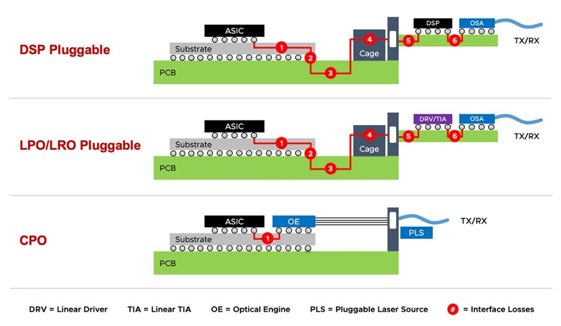
Pluggable optics (today’s mainstream)
Pluggable modules integrate DSP for signal conditioning. This provides robust interoperability but comes with higher power and thermal density.
LPO (Linear Pluggable Optics)
LPO removes the DSP and relies on high-quality SerDes + linear drive to cut power and latency. The tradeoff is tighter channel requirements (cleaner board/package, stricter SI budgets), and often a more controlled, homogeneous deployment environment.
CPO (Co-Packaged Optics)
CPO places the optical engines at/near the switch ASIC package, typically with external lasers feeding light into the co-packaged engines. A widely cited APNIC deep dive reports Broadcom’s claim of roughly ~5.5 W per 800G port for CPO vs ~15 W for equivalent pluggables, implying ~3× power reduction at the port level.
That said, CPO adoption is gated by operational and reliability realities. Reuters reported Jensen Huang stating that while NVIDIA plans to use optical technology in networking switch chips through 2026, broad adoption (especially closer to GPUs) may take until 2028+ due to reliability/serviceability concerns and copper’s proven robustness in some domains.
Supply chain map: what changes as optics move “inward”?
Pluggable era supply chain (QSFP/OSFP)
Key building blocks:
Optical engine / PIC(SiPh or InP)
Lasers(EML/DFB; or CW lasers for SiPh)
Modulators(MZM, micro-ring, etc.)
Drivers / TIAs(analog front-end)
DSP(PAM4, FEC, equalization)
Packaging + test + thermal
Connectors/fiber assemblies

Value capture concentrates in transceiver vendors, optics component suppliers, and DSP/AFE IC vendors.
LPO era: value shifts toward SerDes, channel engineering, and systems co-design
Removing DSP means:
More value sits in switch/accelerator SerDes quality, retimers/redrivers, PCB materials, and connector/channel design.
System vendors must enforce tighter interoperability envelopes.
CPO era: packaging, test, lasers, and optical attach become strategic bottlenecks
CPO compresses the boundary between “network silicon” and “optics,” raising new chokepoints:
Advanced packaging + co-design(substrates/interposers, thermal architecture)
Optical attach/assembly(fiber attach, alignment tolerance, yield learning)
External laser sourcesand optical power budgeting
Test at scale(wafer/module/package-level optical test flows)
In parallel, silicon photonics momentum is accelerating across the ecosystem. Reuters, for example, reported STMicroelectronics launching a data-center photonics chip developed with AWS for transceiver use—highlighting how mainstream semiconductor players are moving deeper into the photonics stack.
2月28日
Laser Technology and Supply–Demand Bottlenecks
Tight EML supply and the rise of high-power lasers
High-end optical modules (especially 800G/1.6T class) and many near-term CPO roadmaps still rely heavily on electro-absorption modulated lasers (EMLs) because EMLs integrate modulation on the same device, delivering strong reach and signal integrity at very high speeds.
The problem is structural: EMLs are hard to make and the supplier base is small.Industry notes that the demand surge from AI data centers has created a major upstream bottleneck in laser light sources, and that NVIDIA has secured a large portion of capacity at key EML suppliers—pushing lead times beyond 2027 and contributing to a global shortage.
On the supply side, Lumentum has also acknowledged a persistent imbalance in EMLs, with demand outpacing supply (even as capacity expands).
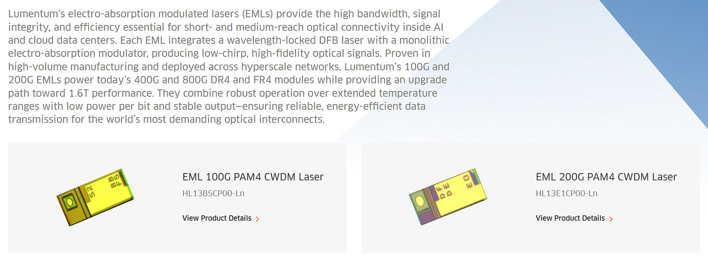
This shortage is one reason hyperscalers and module makers are accelerating alternative architectures, especially external continuous-wave (CW) lasers + silicon photonics modulators, which broaden the supplier pool compared with EMLs. TrendForce explicitly describes CW + SiPh as a major alternative path as the industry works around EML constraints.

2月26日
Why CPO pushes “high-power CW lasers” into the spotlight
Many CPO concepts use external lasers to feed light into co-packaged optical engines. Because CPO architectures must overcome losses from connectors/splitters/couplers and still maintain link margin, the industry is pushing toward hundreds of milliwatts per laser in relevant bands.
Lumentumdemonstrated high-power CW 1310 nm DFB performance, including 580 mW ex-fiber at 50°C in a packaged module, as described in its technical paper.
Coherenthas publicized sampling of >400 mW CW lasers at 55°C with low noise characteristics for CPO/silicon photonics, with volume plans tied to its manufacturing expansion.
Capacity expansion: moving InP manufacturing to 6-inch wafers
To relieve constraints and reduce cost, the industry is scaling compound-semiconductor manufacturing. Coherent announced 6-inch InP wafer fabrication capability, highlighting ~4× more devices per wafer and >60% die cost reduction, and explicitly listed high-speed EMLs, photodetectors, and high-power CW lasers among the product families being qualified on the 6-inch platform.
Supplement: where the next bottlenecks shift
Even if laser die capacity expands, practical throughput can still be limited by:
Epitaxy capacity(InP epi wafers are shared across EML/CW/PD devices)
post-fab processes(die singulation, burn-in/aging, screening)
packaging and fiber attach(alignment yield, thermal handling)
TrendForce specifically flags that CW production also faces constraints due to equipment lead times and labor-intensive reliability steps (e.g., testing/aging), potentially pushing the CW ecosystem toward its own capacity crunch.
2025年5月15日
Reliability challenges: lasers and photodiodes are often the weak link
Laser reliability remains one of the most critical risk factors in optical systems—especially when thermal density rises and maintenance windows shrink in AI clusters.
From an OCP Global Summit 2025 recap, germanium-based photodiodes (Ge PDs) are highlighted as among the most failure-prone subcomponents in photonic systems, with high sensitivity to ESD and other practical handling/design pitfalls.
Why CPO can improve reliability (but also changes the failure model)
CPO can remove some field-replaceable optical parts (pluggables), and it can shift to:
wafer-level testingfor integrated photonic components (better screening earlier)
external laser strategies(depending on architecture) that may simplify certain thermal/aging management
At the same time, CPO introduces new reliability vectors:
package-level thermal-mechanical stress near switch ASICs
optical attach and connector reliability at higher density
serviceability tradeoffs (repair model shifts from module swap to system-level maintenance)
Broadcom/Meta testing results have been used publicly to argue that CPO is approaching production readiness at hyperscale, citing one million cumulative 400G-equivalent port device hours without a single link flap, and reporting ~65% optics power reduction versus pluggables in the same context.
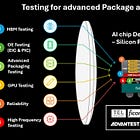
CPO and Optical-Engine Testing: ficonTEC’s Leading Edge
Because co-packaged optics (CPO) places the optical engine in the same package neighborhood as the switch/ASIC, many components become non-field-replaceable. That makes test, screening, and process control a first-order determinant of yield, reliability, and ultimately cost per delivered Tb/s.

2025年4月15日
SemiVision’s key point is directionally correct: before CPO assembly and sealing, manufacturers must complete sub-micron active alignment, die/wafer-level optical yield mapping, and high-speed bit-error-rate (BER) validation—otherwise failures get “buried” inside a package that cannot be serviced.
Why test becomes the bottleneck in CPO
In the pluggable era, a bad module is swapped. In CPO:
A bad optical engine can scrap an expensive assembly (or force rework).
Defect screening must shift earlier (wafer/die level) and become more comprehensive (electro-optical + RF + optical alignment in one flow).
Production needs parallelization (multi-site) to keep test cost from exploding.

ficonTEC platforms that directly target these pain points
1) DLT-D1 multi-site die-level tester (for double-sided compact 3D CPO optical engines)
According to ficonTEC, DLT-D1 is designed to move CPO optical-engine testing from lab-style setups to high-throughput manufacturing. Core capabilities include:
Test coverage from DC parametric through full data-rate RF testing
Bottom-side active optical alignment combined with top-side high-frequency electrical probing
Automated JEDEC tray/magazine handling to fit OSAT / volume production lines
Optional automated fiber coupling (depending on DUT interface)
Up to three parallel test heads to reduce cost per tested unit via true concurrency
2) Wafer-level electro-optical test cells (double-sided / single-sided) to closethe “wafer → die” gap
For silicon photonics and CPO, ficonTEC has also introduced a 300 mm double-sided electro-optical wafer tester concept aimed at high-volume wafer probing, with features such as:
Double-sided probing architecture enabling electrical high-data-rate/DC test on one side and six-axis precision optical active alignment on the other
Automation hooks for manufacturing throughput (e.g., autoloading and calibration concepts are highlighted in these product descriptions)
3) Integration with mainstream ATE: the Teradyne × ficonTEC signal
A major scaling signal is Teradyne’s announcement of a high-volume, double-sided wafer probe test cell for silicon photonics, partnered with ficonTEC—explicitly framed as driven by CPO demand. This matters because it implies CPO testing is converging toward semiconductor-style ATE ecosystems, not bespoke photonics benches.
Teradyne Announces Production System for Double-Sided Wafer Probe Test for Silicon Photonics
What “ficonTEC advantage” really means
SemiVision’s framing—machine vision + 6-DOF alignment + software/AI optimization—maps to a hard manufacturing truth: in photonics, alignment is yield.
Machine-vision assisted 6-DOF active alignment reduces coupling loss variability, enabling tighter BER margins at the same laser power.
Earlier end-to-end validation (wafer/die level) prevents expensive package-level fallout.
Multi-site parallelism (DLT-D1) attacks the biggest hidden cost in photonics: test time per good device.
2025年7月16日
Short-Reach and Ultra-Short-Reach Optical: VCSEL vs. MicroLED
VCSEL: mature workhorse for short reach (≤ a few hundred meters)
850 nm VCSEL + multimode fiberremains a dominant solution for short-reach datacom interconnects because it is:
Mature manufacturing ecosystem
Cost-effective for short reach
Power efficient at practical link budgets
Broadcom’s own component portfolio highlights 850 nm VCSELs explicitly positioned for high-performance short-reach data networks, underscoring how established this path is.
Reality check on “moat”: the module/system differentiation often sits in SerDes quality, packaging, and thermal/SI engineering more than in the emitter itself. VCSEL remains technologically mature—but it’s also why its cost curve is relatively well-known and harder to disrupt without a step-function alternative.
MicroLED: a credible new contender to “replace lasers” in ultra-short reach

MicroLED interconnects are compelling because LEDs do not require laser threshold current and can scale bandwidth through massively parallel channels, potentially reducing energy/bit at the system level.

2025年5月4日
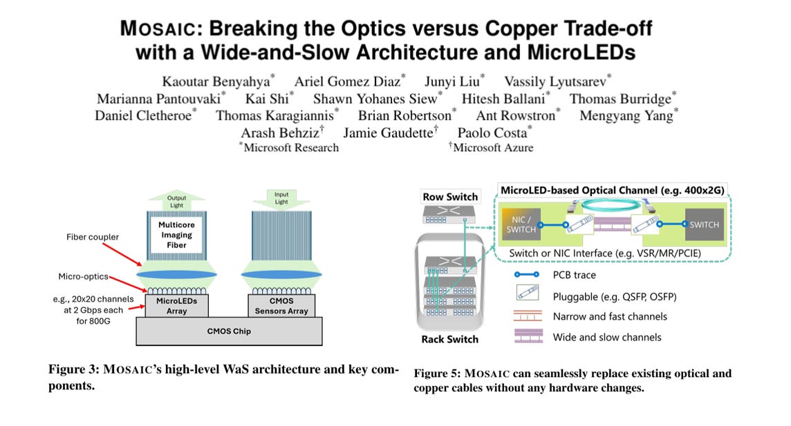
Microsoft MOSAIC (Wide-and-Slow, microLED arrays)
Microsoft’s MOSAIC paper explains the “wide-and-slow” idea: use hundreds of low-speed channels instead of a few ultra-high-speed lanes. It gives a concrete sizing example: assuming 2 Gb/s per microLED channel, an 800 Gb/s link can be built with a 20×20 microLED array that fits in <1 mm × 1 mm die area. The paper also reports up to 68% power reduction and ~10× reach vs copper in its architecture framing.
Avicena LightBundle: microLED + PD arrays hybrid-bonded to CMOS
Avicena positions LightBundle as a microLED-based interconnect platform with:
1 Tb/s per mm “shoreline” I/O density
10 m reach
<1 pJ/bitinterconnect energy efficiency (platform claim)
On ecosystem scale-up, Optica reports Avicena working with TSMC to optimize silicon photodetector (PD) arrays for LightBundle microLED interconnects aimed at AI scale-up networks.
Supercomputing demo signal (reliability + no-FEC angle)
Avicena (and independent trade coverage) reports that at SC25 its LightBundle links operated at 4 Gb/s per lane, closing at raw BER 1×10⁻¹² with ~80 fJ/bit per LED, and notably without forward error correction (FEC)—a meaningful proof point for ultra-low-power, low-latency operation in controlled short-reach scenarios.
MicroLED vs. VCSEL: what’s the real inflection?
VCSELwins today on maturity, volume manufacturing, and known reliability.
MicroLEDwins on the potential to push energy/bit lower via (1) no threshold current behavior and (2) parallelism—especially when paired with CMOS-compatible PD arrays and advanced bonding.
The key risk:microLED interconnect success is less about the LED itself and more about array uniformity, bonding yield, receiver sensitivity, packaging/coupling, and test at scale—which loops back to the earlier point: optical test/assembly tooling becomes strategic as soon as optics move on-package/on-board.

2025年6月15日
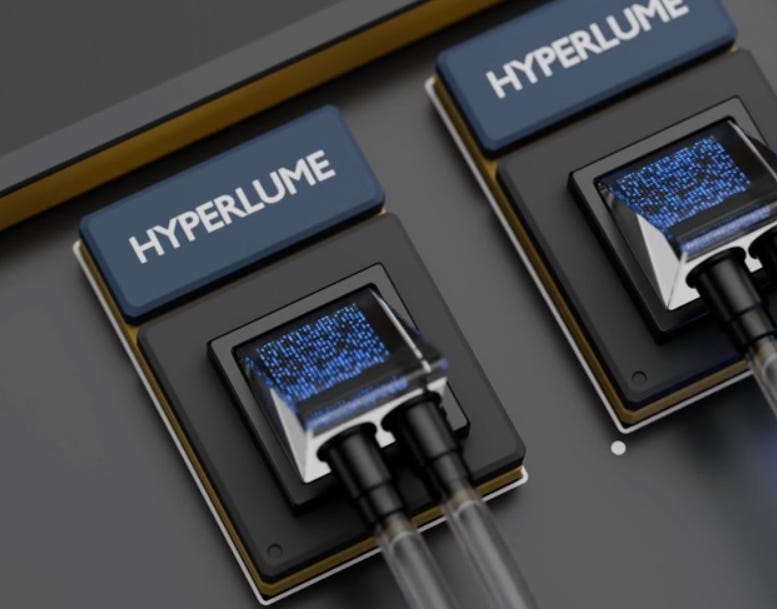
In September 2025, Credo Technology Group acquired Hyperlume. Hyperlume’s micro-LED optical interconnect technology will be integrated with Credo’s end-to-end system-level connectivity solutions, enabling Credo to accelerate its expansion into high-speed interconnect technologies for next-generation AI data infrastructure.

Following the integration of the two product portfolios, Credo’s customers will also gain access to new options for scaling AI networking solutions. This move indicates that Credo has strategically positioned itself to capture opportunities in the emerging micro-LED optical communication market, which could further expand the company’s business scale and diversify its future profit growth drivers.
Scale-out vs. Scale-up: Who’s building what
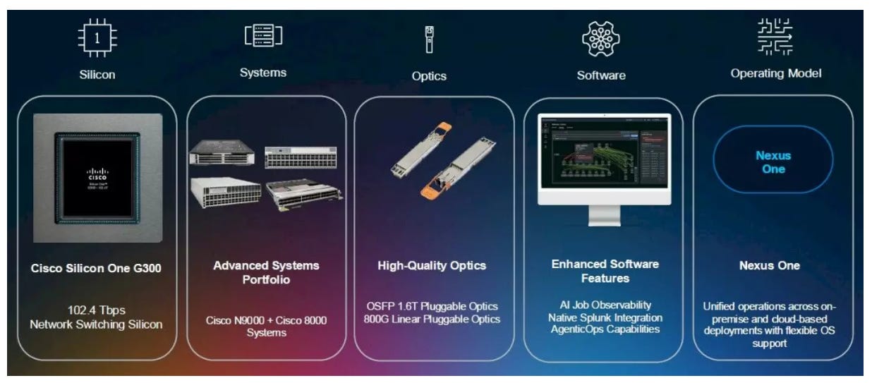
In the scale-out networking market (rack-to-rack / fabric Ethernet), the leading switch ecosystem players include NVIDIA, Broadcom, Marvell, and Cisco—each pushing 51.2T → 102.4T class switch silicon and systems as AI clusters expand. For example, Cisco has publicly announced its Silicon One G300 (102.4 Tbps) positioned for AI backend networks.
In the scale-up domain (GPU-to-GPU / node-local high-bandwidth interconnect), the industry is actively exploring OIO/CPO-style optical links to reduce NVLink-class copper’s power and reach constraints. Companies frequently cited in this direction include Ayar Labs, Marvell, Lightmatter, and Intel, with optical I/O and co-packaged approaches intended to bring optics closer to compute and/or into the package. (Ayar Labs’ OIO positioning is explicitly framed as “in-package optical I/O” vs. CPO trade-offs and roadmap.)
Forward Trends: LPO / CPO / OIO Roadmaps — and “Quantum Interconnect”
LPO: still a large market through this decade
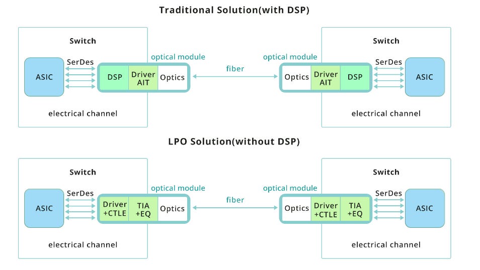
Linear Pluggable Optics (LPO)reduces power and latency by removing the DSP and relying on high-quality SerDes + channel engineering. Practically, LPO tends to scale with the switch/ASIC SerDes generation (e.g., 200G/lane-class electrical I/O enabling 1.6T-class optics), and many deployments will continue to favor pluggables (DSP or linear) for serviceability and operational simplicity.
As switch silicon moves into 102.4T and beyond, the pluggable ecosystem remains the default adoption path because it preserves the field-replaceable module model; this matters a lot for hyperscalers optimizing MTTR and supply-chain flexibility. (Switch silicon and optics roadmaps are converging around 51.2T/102.4T and 1.6T-class links.)

2025年5月24日
CPO: timing depends on test time, KGD, and operational model
CPO mass production schedules are heavily constrained by test throughput and Known Good Die (KGD) availability, because optical engines near/inside the package are not treated as “easy swap” components. Broadcom’s widely cited power claim illustrates why the industry keeps pushing: roughly ~5.5 W per 800G port for CPO versus ~15 W for equivalent pluggables—~3× lower at the port level.
what changes between 2026 → 2028:
Near term, optics are expected to remain pluggable-dominant in many deployments because they are operationally mature and easier to service.
As 51.2T / 102.4T switch capacity and 200G/lane SerDes become pervasive, CPO becomes more attractive to solve board-level electrical reach/power density issues—especially at 800G/1.6T per port.
A practical adoption pattern is: CPO appears first in switch systems (where the form factor and cooling can be designed around it), then expands as test ecosystems and reliability data mature.
OIO (Optical I/O): package-native optical links to enable disaggregation
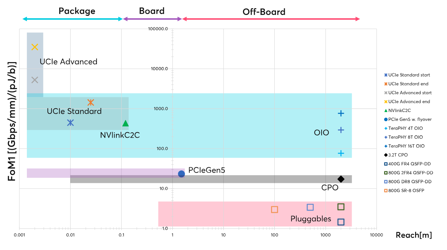
Ayar Labspositions OIO as an “in-package” optical I/O strategy that can bring optical links to the chiplet shoreline, aiming for reach-independent bandwidth scaling without the same electrical distance penalties.
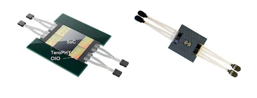
Key published specs (Ayar Labs):
TeraPHY optical I/O chiplet supports a UCIe standard package electrical interface
Publicly described as reaching 8 Tbps bandwidth (generation described in Ayar Labs’ materials)
Uses WDM with 16-wavelength architecture (Ayar Labs describes 16 WDM transceiver slices per optical port; their announcements reference a 16-wavelength light source)
Ayar Labs Closes $500M Series E, Accelerates Volume Production of Co‑Packaged Optics

OIO is structurally aligned with memory disaggregation and large-scale GPU domain scaling because it can extend high-bandwidth links beyond what copper can handle at acceptable power—without forcing every connection into a pluggable module form factor.
In practice, OIO adoption hinges on: thermal robustness near hot compute, stable wavelength control (esp. micro-ring approaches), packaging integration with UCIe ecosystems, and—again—high-throughput test.

1月29日
“Quantum interconnect” (e.g., NVQLink): relevance, but still not the same as NVLink replacement

Today, NVLink remains a copper-based GPU interconnect in mainstream deployments. Looking forward, NVIDIA has introduced NVQLink as an interconnect intended to tightly couple quantum processors (QPUs) with classical accelerated systems (GPUs/CPUs) for hybrid quantum-classical workflows.

Important clarification:
NVQLink is best understood as a quantum–classical system interface, not a near-term drop-in replacement for GPU-to-GPU NVLink inside AI training fabrics.
Quantum advantage is algorithm- and error-correction-dependent, and commercial impact depends on sustained improvements in fidelity and scalable architectures. For instance, IonQ has reported 99.99% two-qubit gate fidelity as a milestone toward fault tolerance.
Conclusion and Outlook
AI-era interconnect demand is accelerating optical evolution across the stack:
Pluggable opticsremain the mainstream delivery vehicle through 400G/800G (and well into 1.6T) because of serviceability and ecosystem maturity.
LPOis a pragmatic “power-down” path for pluggables when deployments can control channel conditions and interoperability.
CPObecomes increasingly compelling as switch bandwidth scales (51.2T → 102.4T) and electrical reach/power density becomes untenable—yet CPO’s ramp depends on test throughput, KGD, and operational acceptance.
OIOpushes optics deeper into the package/chiplet era and ties naturally to UCIe and future disaggregated architectures; the technology promise is strong, but integration/test maturity will determine timing.
As 200G/lane becomes normal, copper’s limits will force continued “optical encroachment” into shorter reaches—making external-laser + CPO/OIO-style architectures a durable long-term direction for hyperscale AI systems.

3月6日

2月26日


PreviousNext
TopLatestDiscussions








See all