Taiwan Is Not Just TSMC: The UMC Story You Need to Know
Taiwan Is Not Just TSMC: The UMC Story You Need to Know
- Source: SemiVision
- Author: SEMIVISION
- Published: 2026-03-05T12:15:09+08:00
- URL: https://tspasemiconductor.substack.com/p/taiwan-is-not-just-tsmc-the-umc-story (1) Taiwan Is Not Just TSMC: The UMC Story You Need to Know


Taiwan Is Not Just TSMC: The UMC Story You Need to Know
Original Article By SemiVision Research [Reading time: 30 mins]

Mar 05, 2026
∙ Paid

With TSMC running at full capacity, the industry is once again searching for additional manufacturing partners. That search is naturally leading many companies to UMC. As demand for semiconductors expands across AI, automotive, and industrial markets, UMC is emerging as a critical part of Taiwan’s broader foundry ecosystem.

We review UMC’s fourth-quarter 2025 performance and its outlook for 2026: United Microelectronics Corporation (UMC) announced its fourth-quarter and full-year 2025 financial results on January 28, 2026, and held an online earnings conference on the same day.

As the world’s second-largest pure-play foundry, UMC specializes in mature process technologies and a diversified portfolio of specialty processes. The information disclosed at the 4Q25 earnings call not only highlights UMC’s operating results for the quarter, but also provides important signals regarding industry trends and the company’s strategic direction for 2026.

Based on the 4Q25 financial statements and earnings-call materials, this article delivers an in-depth analysis of UMC’s financial performance, capacity deployment, technology strategy, international partnerships, forward outlook, and management Q&A. In addition, UMC is actively advancing its silicon photonics initiatives; according to SemiVision’s understanding, these efforts have already achieved encouraging progress.
4Q25 Financial Performance Overview: Revenue and Profitability
United Microelectronics Corporation (UMC) reported consolidated revenue of NT$61.81 billion (approximately US$1.97 billion) in 4Q25, representing a 4.5% quarter-over-quarter increase and a 2.4% year-over-year increase. The revenue growth was primarily driven by favorable foreign exchange movements and higher shipment volumes at the 22 nm and 28 nm nodes. Management emphasized that the growth did not stem from a broad-based demand recovery, but rather from product mix optimization and volume ramp-up at selected process nodes.
Below we will share:
UMC-Wafer Shipments and Capacity Utilization
UMC-Average Selling Price and Product Mix
UMC-Geographic Revenue and Customer Mix
UMC-End-Market Application Mix
UMC-Process Technology Mix
SemiVision’s Perspective on UMC’s Product and Technology Strategy
Detailed Overview of Specialty Process Technologies
Advanced Packaging and Silicon Photonics Technologies
UMC International Collaboration and Capacity Expansion
2026 Guidance and Industry Outlook
Semiconductor Trends and Application Outlook
Competitive Strategy Analysis
2026 Earnings Conference Call Q&A Deep-Dive Analysis

2025年4月6日

Gross margin in 4Q25 reached 30.7%, up 0.9 percentage points QoQ and 0.3 percentage points YoY. Operating margin was 19.8%, improving 1.0 percentage point QoQ and remaining flat YoY. Net margin declined to 16.2%, down 9.1 percentage points QoQ, mainly due to higher income tax expenses, but still 2.2 percentage points higher YoY.
Net income attributable to shareholders in 4Q25 was NT$10.06 billion (approximately US$320 million). Earnings per share (EPS) came in at NT$0.81. Full-year 2025 EPS totaled NT$3.34, reflecting UMC’s ability to maintain stable profitability despite a subdued market environment. Compared with 3Q25 EPS of NT$1.20, the sequential decline in 4Q highlights the dilutive impact of taxes and non-recurring factors.
Wafer Shipments and Capacity Utilization
UMC shipped approximately 994 thousand 12-inch equivalent wafers in 4Q25, flat quarter over quarter. Despite generally soft end-market demand, the company sustained revenue growth through product mix optimization and favorable FX effects. Capacity utilization remained at 78%, unchanged from 3Q25. Utilization staying within the 70–80% range underscores UMC’s stable positioning in balancing supply and demand for mature nodes.
Average Selling Price and Product Mix
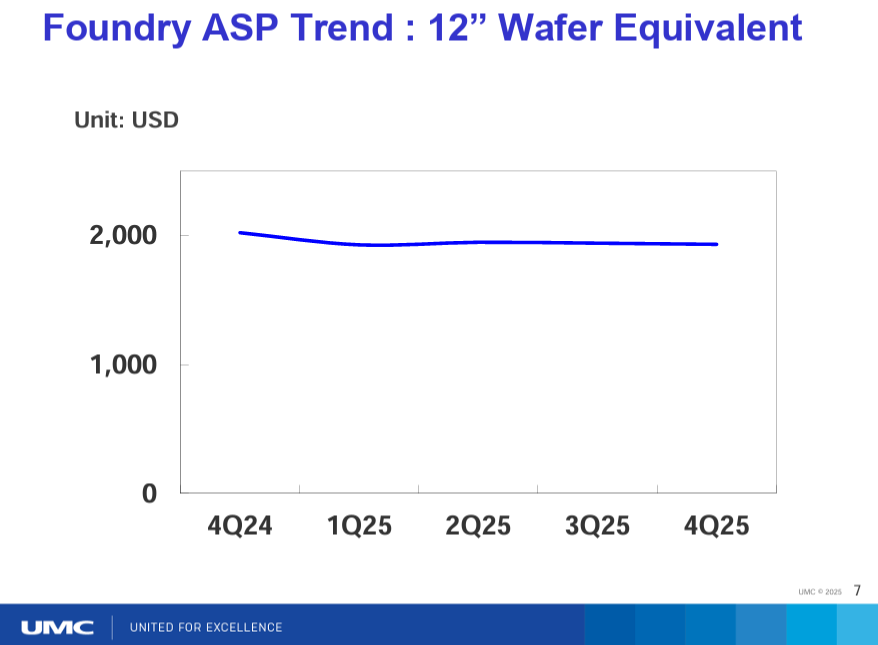
UMC indicated that blended ASP in 4Q25 was largely flat. ASP resilience was supported by an improved product mix, with strong demand at the 22 nm node, which accounted for over 13% of revenue. Combined 22/28 nm nodes contributed 36% of total revenue, serving as the primary growth engine for the quarter. In contrast, demand at other mature nodes (such as 65 nm and 40 nm) remained relatively modest.
Geographic Revenue and Customer Mix
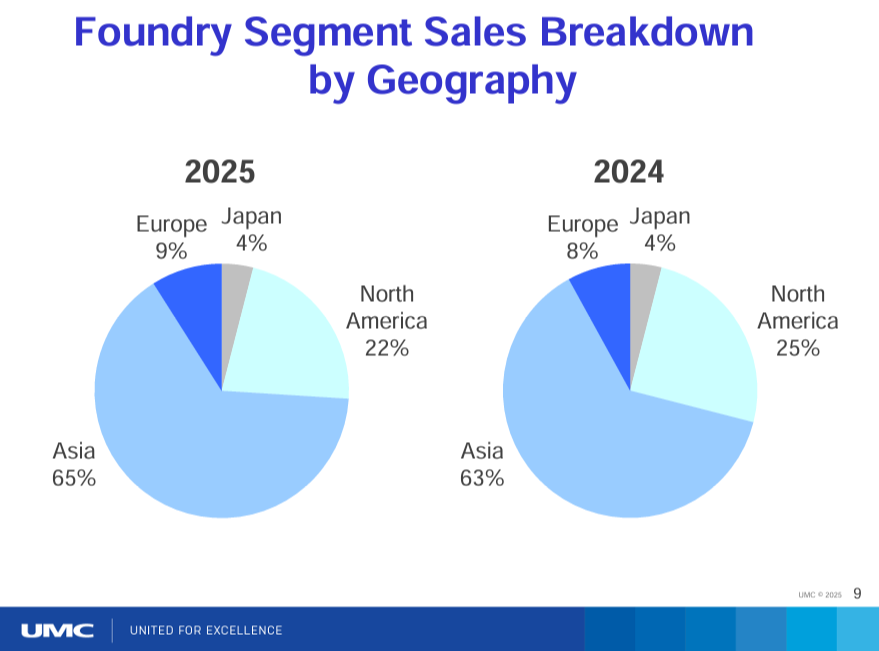
By geography, Asia accounted for 64% of total foundry revenue in 4Q25, followed by North America at 21%, Europe at 11%, and Japan at 4%, largely unchanged from 3Q25. This distribution reflects Asia (including mainland China, Taiwan, and South Korea) as the core demand base for mature-node processes. By customer type, fabless customers represented 80% of revenue, while IDM customers accounted for 20%. Although the fabless share edged slightly lower QoQ, it continued to dominate UMC’s customer base.
End-Market Application Mix
By end application, communications products contributed 42% of 4Q25 revenue, followed by consumer electronics at 28%, computing at 12%, and others at 18%. Compared with 3Q25, the consumer electronics share increased modestly, indicating a recovery in demand for products such as Wi-Fi and set-top boxes. For full-year 2025, the application mix was communications 42%, consumer 28%, computing 14%, and others 16%, highlighting UMC’s heavy exposure to communications and consumer segments.

Process Technology Mix
Revenue by process node in 4Q25 was as follows: 22/28 nm: 36%; 40 nm: 17%; 65 nm: 17%; 90 nm: 8%; 0.11/0.13 µm: 7%; 0.15/0.18 µm: 10%; 0.25/0.35 µm: 4%; ≥0.5 µm: 1%; and ≤14 nm: no contribution. This structure underscores UMC’s focus on mature nodes at and above 22 nm, while leveraging specialty technologies—such as high-voltage, high-current, and non-volatile memory (NVM)—to deliver differentiated value to customers. The strong growth at 22 nm reflects robust demand from mid- to high-end communications and edge AI applications, making it a key area of recent investment.

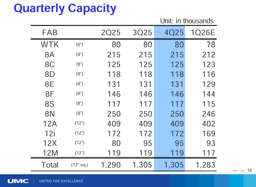
Eight-inch capacity accounts for approximately 40% of UMC’s total capacity, with 12-inch capacity at 60%, indicating continued expansion at 12-inch fabs to support demand for 22/28 nm nodes. Overall capacity increased 1.2% year over year in 2025, and with the completion of Phase 3 of Fab 12i in Singapore, the company expects capacity to gradually ramp from 2026 onward.
SemiVision’s Perspective on UMC’s Product and Technology Strategy
Product and Technology Strategy
Focus on 22 nm / 28 nm and Specialty Processes
UMC regards 22 nm / 28 nm as the golden nodes among mature processes, as they strike an optimal balance between cost efficiency and performance. These nodes address a broad range of applications, including edge AI, data centers, 5G communications, Wi-Fi, digital TV, and automotive image processors. During 4Q25, 22 nm revenue grew 31% quarter over quarter, accounting for more than 13% of quarterly revenue. Management indicated that the 22 nm platform has entered an accelerated harvest phase, with increasing customer tape-outs and wafer starts, and expects 2026 to be another year of growth.
Beyond logic processes, UMC continues to expand the share of specialty processes, which include embedded high-voltage (HV), non-volatile memory (NVM), Bipolar-CMOS-DMOS (BCD), and RF-SOI technologies. These platforms provide one-stop solutions for power management ICs, touch display driver ICs, automotive sensors, and server power management ICs. The company disclosed that specialty processes account for roughly 50% of total revenue, with Power/HV contributing about 30% of that category, while the remainder comes from NVM and VCD (Variable Capacitor Diode) technologies. These offerings typically carry higher margins and stronger customer stickiness, forming the core of UMC’s value proposition.
High-Voltage and Embedded Non-Volatile Memory
Embedded HV processes are a key pillar of UMC’s strategy in power management ICs and automotive markets. As demand rises for electric vehicles, IoT devices, and AI accelerators, the market for high-efficiency power conversion and battery management ICs continues to expand rapidly. By optimizing its HV platforms, UMC enhances breakdown voltage and reliability, enabling higher power density and system stability. Embedded NVM enables programmable access in MCUs and smart sensors, supporting firmware updates and security features. UMC collaborates with multiple MCU vendors to deploy embedded Flash and MRAM, reinforcing its leadership in industrial and automotive applications.
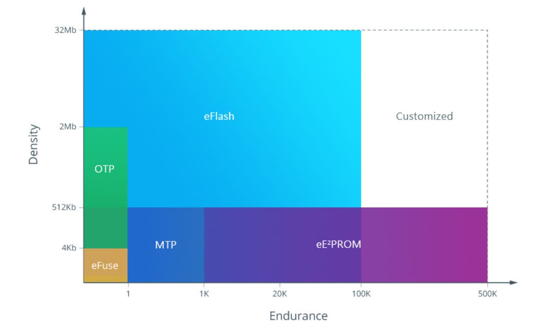

Full Technology Node Coverage
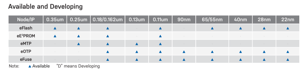
Based on the demanding requirements for increased embedded memory density, higher logic circuitry and IP performance, UMC’s eNVM technology has provided complete embedded memory solutions for 0.35um to 28nm and beyond. These memory offerings are based on a logic/MM process backbone for reliable and compatible eNVM IP integration for customer SoC designs. With UMC’s logic embedded non-volatile memories, customers can adopt standard cell and I/O libraries easily and directly to help customers minimize design efforts. UMC is also developing next generation technology for customers’ future migration needs.
RF-SOI and BCD Integration
With the proliferation of 5G, Wi-Fi 6/7, satellite communications, and millimeter-wave applications, RF circuits increasingly require low-loss, high-linearity transistor structures. RF-SOI (Radio-Frequency Silicon-on-Insulator) offers unique advantages in high-frequency switching, low-spurious filters, and RF front-end modules.

UMC continues to invest in RF-SOI platforms, providing PDKs at 65 nm and 40 nm, and combining them with TSV (Through-Silicon Via) and 2.5D packaging to deliver system-level RF solutions.
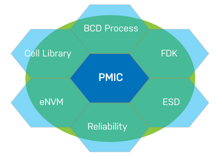
BCD processes, which integrate bipolar, CMOS, and DMOS devices on a single chip, are well suited for power management and motor drive applications. UMC emphasizes that heterogeneous integration of RF-SOI and BCD achieves an optimal balance of performance and cost for communications and automotive power systems.
Detailed Overview of Specialty Process Technologies
UMC’s competitive advantage lies not merely in scale, but in its diverse specialty process portfolio. Key technologies include:
Embedded High-Voltage (HV)
HV processes are designed for power management, LED drivers, display drivers, and motor control. While conventional logic processes typically operate at 1–1.8 V, HV transistors can withstand 20 V, 40 V, or even up to 700 V, enabling simultaneous high-voltage and high-current operation. UMC reduces leakage through SOI structures and thick-oxide designs, and employs LDMOS (Lateral Diffused MOS) devices to improve specific on-resistance while maintaining fast switching under high voltage.
UMC offers HV nodes at 0.18 µm and 0.11 µm, supporting automotive-grade reliability and AEC-Q100 certification, suitable for automotive LED lighting, battery management systems, and fast-charging ICs. By integrating HV with low-voltage logic, customers can implement multi-rail power outputs and intelligent control on a single chip, reducing external components.
Embedded Non-Volatile Memory (eNVM)
With the proliferation of IoT and smart devices, MCUs increasingly integrate logic, sensor interfaces, and program storage on a single chip. Embedded non-volatile memory (eFlash, eEEPROM, MRAM) retains data without power and supports in-field updates.
UMC’s eFlash platforms, based on 55 nm, 40 nm, and 22 nm processes, use SONOS or BE-SONOS memory structures, delivering fast write speeds, low power consumption, and high reliability. For industrial and automotive markets with extreme endurance requirements, UMC also offers embedded MRAM, leveraging magnetic tunnel junctions for high endurance and radiation tolerance. eNVM integration reduces the need for external Flash, shrinks PCB area, and enhances system security—critical for smart appliances, industrial automation, and automotive MCUs.
Bipolar-CMOS-DMOS (BCD) and Power Devices
BCD technology integrates bipolar transistors, CMOS logic, and DMOS power devices on a single chip, ideal for power management, motor drives, and EV charging systems. UMC’s BCD portfolio spans 0.18 µm, 0.11 µm, and even 90 nm nodes, supporting 12 V to 80 V operating ranges.
Using SOI substrates and thick field oxides, UMC’s DMOS devices sustain high voltages while maintaining low on-resistance, suitable for synchronous rectifiers and motor control. Bipolar devices provide high-gain amplification, while CMOS handles digital control and logic. Through BCD platforms, customers can integrate power and control stages on a single chip, reducing system cost and improving efficiency. As automotive and industrial power demand grows, BCD products are becoming increasingly critical.
RF-SOI and RF Modules
RF-SOI isolates devices with an insulating layer, reducing parasitic capacitance and leakage while improving transistor fT and quality factor (Q). UMC offers 0.11 µm, 65 nm, and 40 nm RF-SOI platforms supporting RF switches, low-spurious filters, and low-noise amplifiers (LNAs). The company has also developed integrated passive devices (such as MIM capacitors and spiral inductors) and process tuning techniques to deliver complete RF front-end solutions.
By integrating RF-SOI with BCD and HV, UMC provides highly integrated RF power management modules for 5G smartphones, Wi-Fi routers, and satellite ground terminals.
Automotive Applications of BCD and HV
Automotive electronics are rapidly evolving toward electrification and intelligence. High-power motor drivers, DC-DC converters, and automotive lighting require high-voltage, high-current power devices, while infotainment systems, cameras, and radar demand low-power logic and RF chips. UMC integrates HV, BCD, and RF-SOI platforms to build automotive-grade SoCs.
For example, in ADAS, HV-BCD processes enable multi-phase buck converters alongside RF-SOI front ends for LiDAR or mmWave radar. In EV battery management systems, HV processes deliver high-precision analog front ends, while BCD handles high-current charge/discharge control. These products must comply with AEC-Q100/Q101 and ISO 26262 functional safety standards. Through long-term quality and reliability control, UMC has established a strong reputation in automotive markets.
Digital and Mixed-Signal IP Ecosystem
The success of specialty processes depends on a robust IP and design ecosystem. UMC collaborates with multiple IP vendors to provide standard cell libraries, interface IPs (USB, PCIe, Ethernet), analog IPs (ADC/DAC), and power management IPs across HV, BCD, eNVM, and RF-SOI platforms. This comprehensive IP portfolio enables customers to rapidly build SoCs and shorten development cycles.
UMC also offers Silicon Shuttle (MPW) services, helping small and mid-size customers share mask and prototyping costs, lowering entry barriers. With the rise of open silicon and the RISC-V community, UMC actively partners with ecosystem players to provide open-source cores and accelerator IPs on specialty platforms, fostering long-term ecosystem growth.
Advanced Packaging and Silicon Photonics Technologies
As the semiconductor industry faces the slowing of Moore’s Law, advanced packaging has become a critical lever for further performance gains. United Microelectronics Corporation (UMC) stated that 2026 will mark a key inflection point for advanced packaging and silicon photonics, and that the company has already committed substantial resources and partnered with ecosystem players to develop comprehensive solutions.
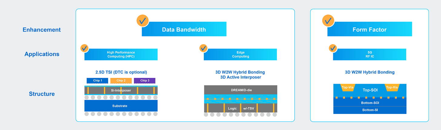
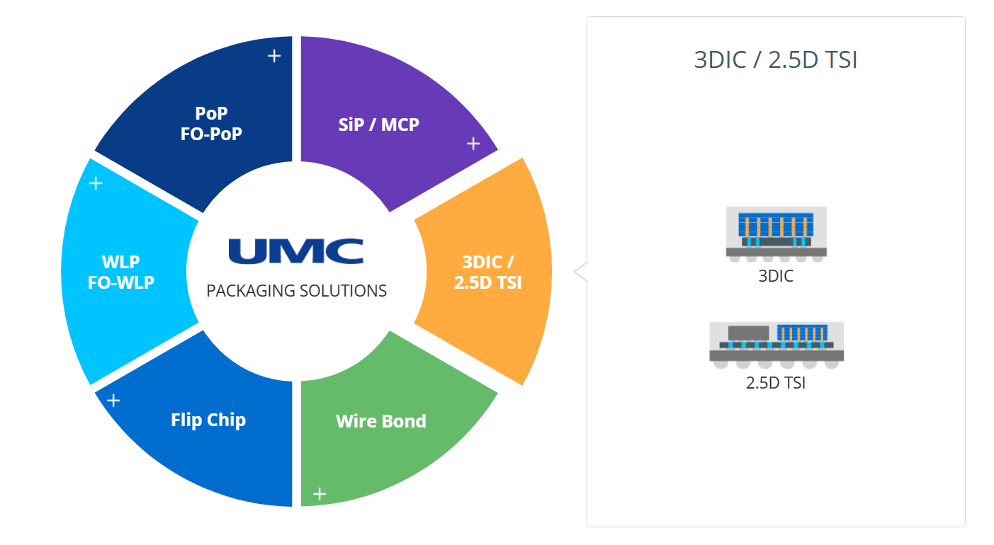
Advanced packaging technologies include 2.5D/3D packaging, wafer-to-wafer bonding, wafer-level packaging (WLP), through-silicon vias (TSV), and interposers. UMC categorizes these efforts into two major areas:
2.5D/3D Packaging on Mature Nodes:
By connecting different chips through interposers or TSVs, logic, RF, and memory dies can be stacked to shorten signal paths, reduce power consumption, and enhance system-level integration. UMC has already introduced stacking technologies into mature processes such as RF-SOI, and has begun volume production.
Heterogeneous Integration for AI Applications:
This approach stacks logic processors with high-bandwidth memory, or integrates multiple dies within a single package using 2.5D interposers, to support high-performance computing requirements in data centers and edge AI. The company disclosed that more than 10 customers are currently engaged in advanced packaging programs, with over 20 new tape-outs expected in 2026. Revenue contributions from these projects are projected to increase meaningfully in 2027.
On silicon photonics, UMC is working with partners to develop a PIC (Photonic Integrated Circuit) platform, covering Optical I/O (OIO), Optical Circuit Switches (OCS), and Co-Packaged Optics (CPO) solutions. The company is targeting a 12-inch silicon photonics platform and plans to offer industry-standard PDKs, with customer delivery targeted for 2027. Compared with competitors that remain on 8-inch silicon photonics, the 12-inch platform offers advantages in cost efficiency and integration. When combined with advanced packaging, it is expected to support data transmission rates exceeding 1.6 Tb/s, as well as future applications such as quantum computing.
UMC International Collaboration and Capacity Expansion
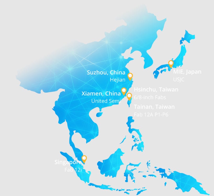
Singapore Fab 12i Phase 3
In 2025, UMC completed Phase 3 of its Singapore Fab 12i expansion, adding 12-inch capacity to support 22 nm / 28 nm nodes and specialty processes. Management noted that the Singapore capacity ramp will begin in 2H26 and continue into 2027, lifting overall company capacity by approximately 1.2% annually. The Singapore fab is a core element of UMC’s supply-chain diversification strategy, enabling service to Southeast Asian, European, and U.S. customers while mitigating geopolitical risk.
UMC’s Singapore Fab 12i Celebrates First Tool Move-In for New Phase 3 Expansion in 2024
12 nm Process Collaboration with Intel
UMC and Intel announced a 12 nm process collaboration in 2025, following a technology transfer/licensing–style model. During the Q&A, management indicated that progress remains on track, with PDK and related IP deliveries expected in 2026, followed by volume production and revenue contribution starting in 2027. Target applications include digital TV, Wi-Fi, and high-speed interface products, strengthening UMC’s U.S. manufacturing footprint and local customer support.

Management remains cautious regarding potential extensions to 10 nm or 7 nm nodes, emphasizing that the near-term priority is the successful delivery and ramp of the 12 nm platform. Any derivative nodes will be evaluated only if technical and commercial conditions align; for now, the company’s focus remains squarely on 12 nm.
MOU with Polar Semiconductor
Beyond the Intel partnership, UMC signed a Memorandum of Understanding (MOU) with Polar Semiconductor in 2025. Polar is a U.S.-based foundry specializing in automotive and high-voltage power ICs.

The collaboration is expected to expand UMC’s capacity access for automotive power management and high-voltage ICs, while accelerating entry into the U.S. supply chain. Although detailed specifications have not been disclosed, management emphasized the win–win and synergistic nature of the partnership.
Xiamen Fab Strategy
UMC’s fab in Xiamen, China, is a key pillar of its geographic diversification. Management noted during the earnings call that the Xiamen fab is currently fully loaded with 100% utilization, with expanding customer engagements. UMC will continue to dynamically optimize customer onboarding and product mix from a regional perspective, serving local customers while reducing geopolitical exposure.
Sustainability and Circular Economy
Alongside capacity expansion, UMC places strong emphasis on environmental and social responsibility. In 2025, the company launched a Circular Economy and Regenerative Innovation Center, establishing waste recycling and processing facilities at its Taiwan sites. This initiative is expected to reduce waste by one-third at Taiwan fabs. UMC has been repeatedly recognized as a leader by CDP, MSCI ESG, and other international assessments, underscoring its commitment to sustainability and corporate governance.

2026 Guidance and Industry Outlook
1Q26 Guidance
Management provided the following1Q26 outlook:
Wafer shipments:Flat QoQ
ASP (USD-denominated):Stable
Gross margin:High-20% range
Capacity utilization:Mid-70% range
2026 CAPEX:US$1.5 billion
This implies a modest sequential decline in gross margin versus 4Q25, driven by higher depreciation and FX movements.

Full-Year 2026 Outlook
Management iscautiously optimisticon the broader semiconductor market in 2026. According to Q&A commentary, AI applications—including data centers and edge AI commercialization—will be the primary growth drivers. While memory supply–demand imbalances may pressure certain consumer electronics segments, the overall semiconductor industry is expected to achieve mid-single-digit growth.
The foundry market, driven by AI, could grow at low-20%, while UMC’s serviceable available market (SAM) is expected to grow at low single digits. The company aims to outperform its SAM average. Full-year 2026 CAPEX is set at US$1.5 billion, allocated to expanding 22/28 nm and specialty capacity, advanced packaging, silicon photonics, and R&D capabilities.
Management believes the 22 nm platform has entered an accelerated harvest phase. New processes and solutions—such as embedded HV, eNVM, RF-SOI, and TSV—are expected to ramp further in 2026, making the year another growth year. With AI-driven structural demand and constrained mature-node supply, UMC expects to gain pricing and margin leverage.
Pricing Environment and Margins
The ASP environment for mature nodes is expected to improve versus 2025, supported by product mix optimization, better utilization, and reduced exposure to commoditized markets. Strong demand at 22 nm underpins pricing. While management does not comment on individual product pricing, it noted that the overall pricing environment is turning more favorable. Even where prices were set earlier in the year, UMC remains open to repricing discussions should market conditions tighten or costs rise.
For margins, 1Q26 gross margin is expected in the high-20% range, with full-year margins influenced by utilization, mix, and FX. Depreciation is projected to increase at a low double-digit percentage YoY, while materials and energy inflation remain headwinds. UMC aims to sustain stable EBITDA through cost controls and efficiency gains.
Supply–Demand Dynamics and Mature-Node Opportunities
Management characterized the current mature-node cycle as structural and AI-driven, rather than cyclical. AI investments prioritize advanced nodes, crowding out new mature-node capacity, while economics for greenfield mature-node fabs remain unattractive—suggesting prolonged supply constraints. Compared with the pandemic-era shortage of 2021, this cycle may last longer and is still in its early stages. On the demand side, recovery in analog and MCU applications is improving the supply–demand balance, reinforcing a more favorable pricing environment for mature nodes.
Semiconductor Trends and Application Outlook
Artificial Intelligence and Hyperscale Computing
AI is the primary engine of semiconductor demand growth. While advanced nodes (<5 nm) benefit from AI training, AI also drives strong demand for edge and peripheral chips. AI servers require power management ICs, optical interconnect components, and sensor controllers, most of which are built on 40 nm and above. UMC’s 22/28 nm HV and BCD platforms serve server power modules and AI accelerator power delivery, while RF-SOI supports high-speed optical transceivers—allowing UMC to benefit from AI without competing at the most advanced nodes.

Electric Vehicles and Autonomous Driving
Automotive electronics are shifting toward electrification and high-performance compute. EVs require power MOSFETs, BMS ICs, onboard chargers, inverters, and motor drivers, while autonomous systems demand mmWave radar, LiDAR, image processors, and AI inference engines. These chips face harsh environments and stringent safety requirements, favoring mature nodes with proven reliability. UMC’s HV, BCD, eNVM, and RF-SOI platforms support AEC-Q100/Q101 compliance, while advanced packaging and silicon photonics extend into automotive high-bandwidth connectivity. As semiconductor content per vehicle rises from ~US$400 (2020) to ~US$1,500 (2030E), UMC sees long-term growth.

IoT and Consumer Electronics
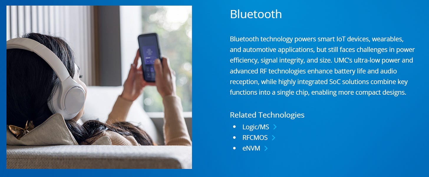
Smart appliances, wearables, and IoT endpoints rely on low-power MCUs, Bluetooth/Wi-Fi SoCs, sensors, and PMICs—prioritizing cost, power efficiency, and integration over leading-edge nodes. Mature processes excel here, especially with eNVM, RF modules, and mixed-signal IP. UMC’s 55/40 nm eFlash and 22 nm eMRAM platforms suit MCUs, while 40 nm RF-SOI supports Wi-Fi 6/7. Despite macro volatility, long-term smart home and health monitoring trends remain supportive.


Industrial Control and Energy Management
Industrial automation and smart manufacturing demand high-reliability controllers, sensors, and drivers operating in harsh conditions. UMC’s HV and BCD processes support PLCs and servo drives, eNVM provides on-chip non-volatile storage, and RF-SOI enables factory wireless connectivity. In energy applications—solar inverters, energy storage, smart grids—mature nodes’ voltage tolerance is a key advantage. Global decarbonization initiatives sustain long-term demand.

Communications and Data Centers
The expansion of 5G, Wi-Fi 7, and LEO satellite communications drives RF front-end demand. UMC’s RF-SOI supports switches, LNAs, and isolators above 6 GHz. Data centers require high-speed optical modules and PMICs; silicon photonics and advanced packaging significantly boost bandwidth while reducing power. The 12 nm Intel collaboration targets digital TV and Wi-Fi, with potential extensions to high-speed interfaces and network controllers—making mature-node chips indispensable as data traffic explodes.
Advanced Packaging and Silicon Photonics: The Next Growth Engine
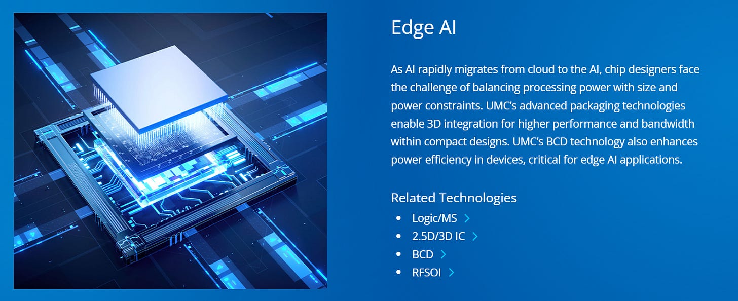
Advanced Packaging Categories and Applications
UMC views advanced packaging as a major post-2026 growth driver, divided into two areas:
2.5D / 3D Packaging and Wafer Stacking:
Applied to mature nodes and RF-SOI, enabling vertical and horizontal integration of logic, RF, and memory. UMC has entered volume production for select customers and expects 20+ new tape-outs in 2026.
AI and High-Performance Packaging:
Involving logic–memory stacking, die-to-die interconnects, and chiplet integration for data centers and edge AI. Over 10 customers are engaged, with meaningful revenue contribution beginning in 2027.

Capacity Expansion and Investment Timing
Advanced packaging capacity will scale with customer ramps. 2026 focuses on materials and technology readiness, while capacity expansion is more likely in 2027, aligned with customer mass production. Current interposer output leverages shared equipment on 40 nm and 65 nm lines; dedicated tool investments, if required, would likely occur in 2027.
Silicon Photonics Products and Roadmap
Silicon photonics integrates optical components on silicon to overcome electrical interconnect bandwidth limits. UMC’s portfolio spans PIC, OIO, OCS, and CPO, with industry-standard PDKs targeted for 2027 delivery.
On timing, 12-inch PIC initially focuses on pluggable modules, with volume ramp starting in 2026. Longer term, integration with advanced packaging and heterogeneous materials will support >1.6 Tb/s transmission and future applications such as quantum computing. Compared with peers still on 8-inch lines, UMC’s 12-inch silicon photonics platform offers clear advantages in cost, scale, and integration.
UMC and the Global Foundry Landscape
Global Foundry Dynamics
The global foundry market has long been dominated by Taiwan Semiconductor Manufacturing Company (TSMC), which leads in advanced nodes with clear technology advantages and economies of scale. United Microelectronics Corporation (UMC), by contrast, focuses primarily on mature and specialty processes, forming a complementary relationship with TSMC rather than competing head-on at the leading edge.
Other key competitors include China’s Semiconductor Manufacturing International Corporation (SMIC) and Hua Hong Semiconductor (HHGrace), Korea’s Samsung Foundry, and U.S.-based GlobalFoundries. Samsung competes most directly with TSMC at advanced nodes, but its market share in mature processes remains relatively limited. GlobalFoundries has exited the race for leading-edge nodes in recent years, concentrating on technologies at 12nm and above while emphasizing partnerships with the U.S. government and automotive customers. SMIC, despite strong policy support, faces constraints in acquiring advanced equipment due to U.S. restrictions and therefore remains concentrated on 28nm and above.
Compared with these peers, UMC’s differentiated strengths include:
Deep expertise in mature nodes:UMC has built long-term capabilities across the 28nm–65nm range, supported by extensive process know-how and a broad customer base. These nodes cover the majority of MCUs, PMICs, connectivity chips, and image processors—core components for IoT and automotive markets.
A comprehensive specialty-process portfolio:From HV, BCD, and eNVM to RF-SOI, UMC offers a full suite of platforms with proven mass-production experience—distinct from TSMC’s strategy, which is more heavily centered on advanced logic nodes.
Geographic diversification:UMC operates fabs in Taiwan, Singapore, and Xiamen (China), and is also building U.S. capacity through partnerships, helping mitigate geopolitical risk.
A stable and diversified customer base:UMC primarily serves fabless customers across networking, consumer, automotive, and industrial segments. This breadth reduces exposure to volatility from any single end market.
Relationship with TSMC and Competitive Positioning
While TSMC is the flagship of Taiwan’s semiconductor industry, UMC’s strategy is not to challenge TSMC at the cutting edge. Instead, UMC positions itself as a leader in mature and specialty processes. The two companies differ clearly in capacity and node strategy: TSMC is anchored on 5nm, 3nm, and increasingly 2nm, serving large customers such as Apple and Qualcomm; UMC focuses on the 22nm–0.5µm range, providing stable supply for a large base of small-to-mid-sized fabless companies as well as automotive and industrial supply chains. This division of labor reduces direct rivalry and gives Taiwan broad node coverage across the global semiconductor supply chain.
During periods of global shortages (such as the 2020–2021 pandemic-driven cycle), both UMC and TSMC raised prices for mature nodes, but UMC benefited more due to its greater exposure to these processes. More recently, as AI investment has concentrated on advanced nodes, TSMC’s capacity expansion has been centered on 3nm and 2nm, with comparatively limited incremental investment in mature capacity. This creates an opportunity for UMC to strengthen its 22nm/28nm footprint, lift ASPs, and capture share from competitors.
Competitive Strategy Analysis
SMIC
Due to U.S. technology restrictions, SMIC has difficulty acquiring EUV and the latest-generation DUV equipment. As a result, its technology progress has largely remained at the 14nm node, with production primarily serving China’s domestic market. Although the Chinese government is actively promoting semiconductor self-sufficiency and “de-Americanization,” SMIC’s yield performance and process quality in mature nodes still lag behind leading Taiwanese foundries.
For UMC, SMIC represents competition mainly within China for certain 28nm–65nm capacities. However, in high-reliability specialty processes, SMIC continues to face a meaningful gap compared to UMC.

2025年3月26日
GlobalFoundries (GF)
After exiting advanced-node development, GlobalFoundries shifted its focus to mature technologies at 12nm and above, emphasizing partnerships with the U.S. government and automotive customers. For example, GF provides 55nm BCD capacity for U.S. defense and automotive applications and highlights its manufacturing presence in Arizona and New York.
UMC and GF compete in mature-node segments, but GF’s product focus is more concentrated on telecom, aerospace, and other high-reliability markets, creating some differentiation in customer base. UMC’s collaboration with Intel to introduce 12nm process technology in the U.S. strengthens its ability to compete more directly with GF in this space.

Hua Hong Semiconductor (HHGrace)
Hua Hong primarily provides processes in the 90nm–0.18µm range, with a strong focus on power semiconductors and discrete devices. It is particularly competitive in 8-inch HV and BCD technologies, though its overall capacity scale is relatively smaller.
UMC holds advantages in mass-production experience across HV, BCD, and RF-SOI, as well as in its 12-inch wafer footprint, enabling it to attract a broader international customer base. In contrast, Hua Hong remains more concentrated on China’s domestic market.
Samsung Foundry
Samsung competes aggressively at advanced nodes but maintains a relatively limited scale in its mature-node foundry business. Its 28nm and 65nm platforms primarily serve internal SoC demand and a limited number of third-party customers, and therefore do not constitute a large-scale competitive threat to UMC.
Samsung and GlobalFoundries previously co-developed 28nm FD-SOI technology; however, market adoption has remained relatively limited.

3月2日
Strategic Outlook
The comparison above illustrates UMC’s comprehensive advantages in the mature-node segment. Looking ahead, AI-related applications and automotive electronics are expected to generate new growth drivers. To maintain its competitive position, UMC must continue to enhance capacity utilization, optimize product mix, and strengthen customer service capabilities in order to stay ahead in an increasingly dynamic global foundry landscape.

2026 Earnings Conference Call Q&A Deep-Dive Analysis
The following summarizes and analyzes the key Q&A discussions from the earnings conference call, outlining management’s views on market dynamics, pricing trends, capacity strategy, and technology development.
Semiconductor and Foundry Market Outlook for 2026
Management believes that the primary growth driver for the semiconductor industry in 2026 will come from AI-related applications, particularly the commercialization of data center and edge AI. While the memory market may experience supply–demand imbalances that could impact certain consumer electronics segments, the overall semiconductor industry is still expected to achieve mid-single-digit growth. The foundry sector, driven by AI demand, could see low-20% growth.
United Microelectronics Corporation estimates its serviceable market will grow at low single digits, with the company aiming to outperform the broader market. This view reflects AI’s structural impact in supporting semiconductor demand and highlights how mature-node processes can still benefit from AI-related peripheral chips and specialty technologies.
Mature-Node ASP Outlook and Pricing Strategy
The ASP environment for mature nodes in 2026 is expected to improve compared with 2025. Key drivers include product mix optimization, higher capacity utilization, and reduced exposure to highly commoditized markets. Strong demand for 22 nm processes is also expected to support overall pricing.
Management noted that it does not comment on pricing for specific products, but the overall pricing environment is becoming more favorable. Pricing negotiations will remain ongoing. Even if some prices were finalized at the beginning of the year, adjustments may still occur if market conditions tighten or costs increase. This flexible pricing strategy helps the company maintain competitiveness amid supply–demand fluctuations.
Supply–Demand Shifts in Mature Nodes and Emerging Opportunities
As the industry reallocates investment toward AI-driven advanced nodes, mature-node capacity may face long-term supply constraints. UMC views this as an opportunity to optimize its product mix and improve ASP and gross margins, while remaining open to new opportunities that support customer demand.
Management emphasized that the current supply–demand shift is structural, unlike the shortage cycle in 2021 that was driven primarily by pandemic-related demand spikes and supply chain disruptions. Today, AI investment is pushing leading-edge development toward smaller nodes, while the economics of building new mature-node fabs remain less attractive, potentially leading to a prolonged tightening of supply.
Singapore Expansion and Depreciation Trends
Overall capacity is expected to grow by approximately 1.2% in 2026. Capacity expansion in Singapore is scheduled to begin in 2H26 and continue into 2027.
Depreciation expenses are projected to increase by low double-digit percentages year-over-year, with similar levels expected in 2026 and 2027. Depreciation could peak in either of those years. While higher depreciation will place pressure on gross margins, increased production from 22 nm capacity and an improved product mix should allow the company to maintain gross margins above 20%.
Capacity Utilization and Cost Pass-Through
When capacity utilization remains in the mid-to-high 70% range, the question arises whether rising costs can be passed on to customers. Management indicated that pricing discussions are ongoing and that market dynamics in 2026 appear more favorable than in previous periods.
Some customers have already accepted adjusted pricing, while others implemented one-time price adjustments at the beginning of the year. Overall, the pricing environment has improved compared with previous cycles. However, while utilization influences ASP, the company aims to maintain long-term competitiveness for both itself and its customers rather than passing all cost increases directly to the market.
Flat Shipments During the Seasonal Slow Quarter
The first quarter is typically a seasonal low point, but the company expects 1Q26 wafer shipments to remain roughly flat compared with 4Q25.
From an application perspective, revenue contribution from consumer electronics increased, driven primarily by Wi-Fi and set-top box demand. In addition, strong demand for image signal processors (ISP) and display driver ICs (DDI) in communications and automotive applications supported shipments. Management believes the first-quarter performance aligns with normal seasonal patterns rather than inventory restocking.
Seasonality and Growth Drivers in 2026
Management expects 2H26 to outperform 1H26, making 2026 an overall growth year, although the pattern may differ from traditional seasonality.
This growth will be supported by several specialty technology projects, including embedded high-voltage solutions, non-volatile memory, power management ICs, and RF-SOI processes. These technologies are being adopted in communications, consumer electronics, automotive, and AI server applications. Many of these projects are expected to ramp in 2H26, driving stronger growth in the second half of the year.
Growth Drivers: Market Share Gains vs. End-Market Recovery
The company emphasized that its growth assumptions are primarily based on market share gains across multiple applications, rather than relying on a strong recovery in end markets such as smartphones, TVs, or PCs.
Although end-market demand has not fully rebounded, UMC has observed increasing customer adoption and share gains in areas such as Wi-Fi chips, automotive imaging processors, and power management ICs. Through its strengths in specialty processes and reliability, the company aims to capture additional market share even during periods of softer industry demand.
Market Rumors About Potential Customers
There have been market rumors suggesting that UMC may be collaborating with certain major chip design companies. However, the company declined to comment on specific customers due to confidentiality agreements.
For investors, management suggests focusing on the company’s technology roadmap and adoption progress, rather than speculation about individual customers.
Advanced Packaging and Silicon Photonics: A Strategic Turning Point
UMC views 2026 as a key inflection point for advanced packaging and silicon photonics, and the company has already begun investing resources and collaborating with partners in these areas.
Advanced packaging is no longer limited to high-end data center applications; it is gradually expanding into mature-node processes and broader markets. This trend could help improve product differentiation, ASP, and long-term gross margins.
The company’s advanced packaging capabilities extend beyond a single component such as interposers. Its portfolio includes wafer-to-wafer stacking, TSV technology, interposers, and 2.5D integration, enabling stacking of logic chips with customer-supplied memory wafers for applications across mobile devices, AI, power management, and other end markets.
Specific Opportunities and Application Areas
During the call, management highlighted two main categories of opportunities in advanced packaging:
Expansion of 2.5D/3D packaging and wafer-to-wafer stacking into mature nodes, including RF-SOI technologies that have already entered mass production.
AI-driven logic and memory stacking, including die-to-die interconnect architectures.
The company disclosed that more than 10 customers are already engaged in advanced packaging projects, with over 20 new tape-outs expected in 2026. Revenue contributions could become significant by 2027.
Capacity expansion will follow customers’ production ramp schedules. In 2026, the focus will primarily be on technology and material preparation, while larger-scale expansion may occur in 2027.
Silicon Photonics Platform and Competitive Advantages
The silicon photonics market is expanding rapidly, driven by demand for high-speed optical interconnects in data centers and the need for high-bandwidth, low-latency data transmission for future AI models.
UMC is focusing on a 12-inch silicon photonics platform and collaborating with partners to develop industry-standard PDKs. Combined with advanced packaging capabilities, this approach enables integrated solutions.
Compared with competitors still relying on 8-inch processes, UMC’s 12-inch platform offers advantages in cost and scale, supporting larger die sizes and higher production output.
The company is targeting PIC, OIO, and OCS solutions, focusing on pluggable or modular architectures rather than solely pursuing full CPO implementations. This strategy aligns better with current market adoption timelines while leveraging the company’s strengths in 12-inch manufacturing and advanced packaging.
Progress of the 12 nm Collaboration and Future Expansion
Regarding its 12 nm collaboration with Intel, management stated that the partnership is progressing smoothly. The PDK and related IP are expected to be delivered in 2026, with product ramp and revenue contribution beginning in 2027.
Target applications include digital TV, Wi-Fi, and high-speed interface products. While the commercial model details have not been disclosed, the company believes the partnership offers strong synergies.
As for extending the collaboration to more advanced nodes such as 10 nm or 7 nm, management indicated that the current priority is to execute the 12 nm program successfully before evaluating future expansion opportunities.
Other Key Topics: Memory Prices, Customer Demand, and Non-Volatile Memory
Regarding rising memory prices, the company stated that it has not yet observed a meaningful impact on customers’ full-year demand forecasts. UMC primarily serves mid-to-high-end markets, including RF front-end modules, Wi-Fi chips, and automotive sensors. These segments tend to demonstrate stronger demand resilience and often receive priority supply during memory shortages.
For non-volatile memory and server power management ICs, the company does not disclose revenue by individual product categories. Instead, it reports them within the specialty process segment, which accounts for approximately 50% of total revenue. Within this segment, Power/High Voltage technologies represent about 30%, with the remainder contributed by non-volatile memory and VCD processes.
As demand for power management ICs in servers and AI systems continues to grow, this product category is expected to expand further.
Gross Margin Outlook and Cost Pressures
Gross margin trends will depend on capacity utilization, product mix, and currency fluctuations. For 1Q26, gross margin is expected to remain in the high-20% range, mainly due to higher depreciation expenses.
Full-year depreciation is projected to increase by low double-digit percentages, while the company also faces inflationary pressures in raw materials and operating costs. Through cost control and operational efficiency improvements, management aims to maintain stable EBITDA performance despite rising capital expenditures.
Future Revenue Contribution from Advanced Packaging
Currently, advanced packaging serves only a limited number of customers and applications. However, with more than 20 new tape-outs expected in 2026, the company anticipates significant revenue growth from this segment by 2027.
Although its share of total revenue will remain relatively small in the short term, advanced packaging has the potential to become a major long-term growth driver. Management emphasized that this technology can enhance both ASP and gross margins, making it a key component of the company’s strategic roadmap.
Market Rumors and Pricing Re-Negotiation
The company declined to comment on rumors regarding potential new customers. Regarding whether customers who previously secured favorable pricing could renegotiate later, management stated that pricing discussions will remain ongoing.
Even if some pricing agreements were finalized earlier in the year, renegotiations may occur if market conditions tighten or costs rise. This continuous dialogue with customers is a standard industry practice.
Management also noted that the improving pricing environment for mature nodes is primarily driven by supply contraction and gradual demand recovery, rather than reliance on any single customer.

2月23日


PreviousNext
TopLatestDiscussions








See all