AI Networking Arms Race Heats Up: 800G Today, 1.6T Tomorrow
AI Networking Arms Race Heats Up: 800G Today, 1.6T Tomorrow
- Source: SemiVision
- Author: SEMIVISION
- Published: 2026-03-04T09:12:28+08:00
- URL: https://tspasemiconductor.substack.com/p/ai-networking-arms-race-heats-up (1) AI Networking Arms Race Heats Up: 800G Today, 1.6T Tomorrow


AI Networking Arms Race Heats Up: 800G Today, 1.6T Tomorrow
Original Article By SemiVision Research [Reading time: 20 mins]

Mar 04, 2026
∙ Paid

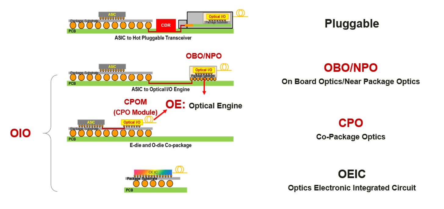
SemiVision will examine demand for 800G and 1.6T optical modules within the broader evolution of AI data center interconnect architectures—from Ethernet/InfiniBand–based scale-out networking (inter-rack and inter-device connectivity), to higher bandwidth density and lower power paths that bring optics closer to the chip (CPO/OIO), and further to the rapid rise of Optical Circuit Switching (OCS) driven by AI clusters that favor more stable, circuit-like data flows.
Our core view is as follows: 800G will remain the primary data rate for large-scale (scale-out) deployment around 2026, while the timing and magnitude of 1.6T demand are more tightly coupled to the maturity of the 200G/lane ecosystem, switch silicon port-speed transitions, and architectural choices inside large AI clusters (including OCS and CPO/OIO).
Below we will share
Supply-Side Constraints and Enablers
Demand Dynamics in AI Interconnects: Pace and Structural Drivers
Layered Evolution: 800G and 1.6T Are Not Simple Replacements
Timing Outlook for 1.6T Adoption
Technology Foundations: Scalable Conditions from 800G to 1.6T Through Standards and Form Factors
Supply Side and Bottlenecks: How Lasers, Silicon Photonics, and Manufacturing Engineering Define the Delivery Ceiling
OIO: From CPO to “In-Package Optical I/O,” and Its Key Components and Mass-Production Barriers
Key Components: From External Cabling to High-Precision Internal Optical Connections
OCS: From Electrical Switching to the Optical Path Layer—and Why It Is Gaining Momentum in AI Clusters
Technology Paths and Engineering Challenges
Taiwan: A Central Hub for Wafer Manufacturing, Advanced Packaging, System ODM, and Passive Components
Japan: Long-Standing Strengths in High-Reliability Materials, Optical Devices, Connectors, and Precision Manufacturing
United States: System and Switch-Silicon Leadership, Key Optical Components, and the Most Active OCS Ecosystem
Europe: Stronger Momentum in OCS and Programmable Photonics, Supported by MEMS and Optical Manufacturing
China: Strength in Large-Scale Optical Module Manufacturing, Expanding Toward Components and System Co-Design

2025年12月31日
Demand Signals and Market Consensus
From the demand side, a consistent signal across multiple research firms is that shipments and penetration of 800G and above are entering a phase of accelerated adoption toward becoming the default configuration. Current projections indicate that shipments of 800G+ optical transceivers will rise sharply in 2026, with their share of total shipments exceeding 60% that year. At the same time, upstream laser light source supply is increasingly identified as a potential bottleneck.
Meanwhile, research firms note that 800G will be the fastest-growing datacom optical segment in 2025, whereas 1.6T, despite entering volume production in select use cases in 2025, will remain below the million-unit level for the year. True volume expansion for 1.6T is expected only after platforms and ecosystems further mature.
Supply-Side Constraints and Enablers
From the supply side, the most critical conclusion is that components and manufacturing capacity tied to 200G/lane—particularly InP lasers/EMLs and their capacity expansion cadence, silicon photonics combined with advanced packaging, and testable/maintainable engineering solutions—will determine whether 1.6T transitions from limited deployment to end-to-end scale. We view laser light source shortages as one of the key constraints around the 2026 timeframe.
Demand Dynamics in AI Interconnects: Pace and Structural Drivers
AI cluster networking differs from traditional data centers in two key ways. First, training and inference traffic exhibits stronger synchronization and collective communication patterns. Second, bandwidth density within a single rack or pod continues to rise, pushing electrical interconnects toward physical limits in loss, power consumption, routing complexity, and maintainability. Together, these forces drive the parallel evolution—not substitution—of higher-speed pluggable optics (800G → 1.6T) and optics closer to the chip (CPO/OIO).
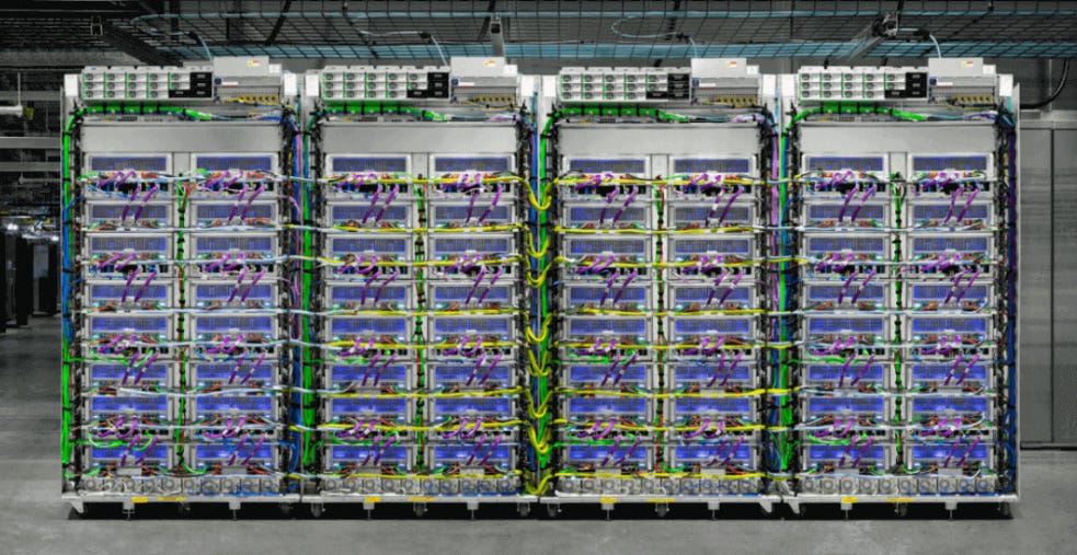
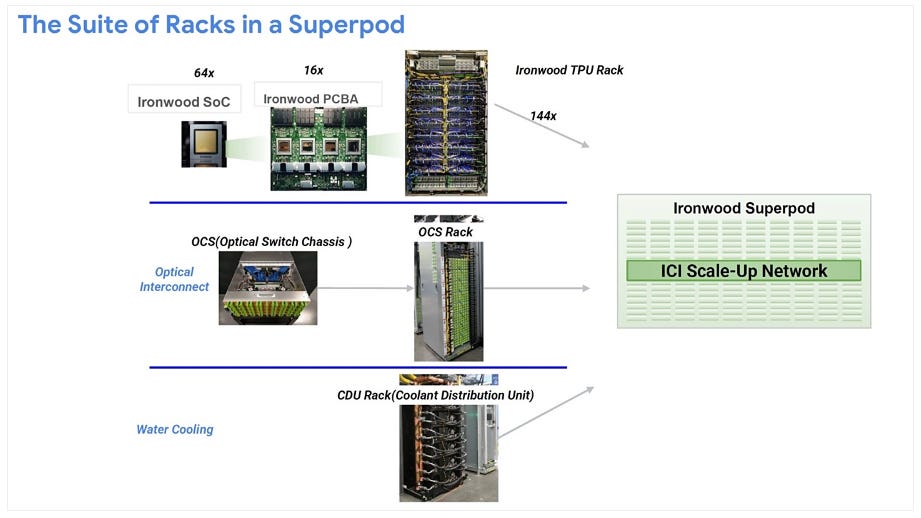
In February 2026, further analysis cited Google’s next-generation TPU interconnect architecture as an example, noting that in OCS-participating all-optical network designs, clusters are provisioned with substantial volumes of 800G/1.6T modules from the outset—suggesting that demand from this architecture alone could exceed the million-unit level.
Layered Evolution: 800G and 1.6T Are Not Simple Replacements
Structurally, demand for 800G and 1.6T follows a layered evolution, rather than a straightforward generational replacement.
Layer 1: Scale-out (inter-rack / inter-device).
Based on public disclosures around next-generation photonic switching platforms, AI factory–scale networks are pushing switch port capabilities toward 1.6 Tb/s per port, while retaining flexible port breakout options (e.g., more 200G ports or fewer 800G ports) to accommodate different topologies and deployment densities. As a result, 800G will remain the mainstay for near-term large-scale deployment, while 1.6T is more likely to appear first in newly built clusters based on next-generation switch silicon and network architectures.
Layer 2: Scale-up (intra-rack / intra-node).
Public materials related to next-generation AI platforms emphasize tighter dependence on 200G SerDes and co-packaged optics for future AI factories, with related products and systems expected to be delivered through partners starting in the second half of 2026. These signals point to a clear reality: as bandwidth density requirements within racks and nodes continue to rise, traditional pluggable form factors face increasing pressure in power, size, routing, and maintenance—making OIO a structural mid- to long-term direction.
Timing Outlook for 1.6T Adoption
Across the industry, expectations for when 1.6T ramps meaningfully are closely aligned with 200G/lane ecosystem maturity. Cignal AI explicitly notes that while 1.6T enters volume production in select scenarios in 2025, overall scale remains limited. A broader transition toward 1.6T will unfold gradually thereafter. Multiple well-known research firms similarly indicate that deployments will occur in 2025–2026, but that the acceleration point is more likely after 2027.
Technology Foundations: Scalable Conditions from 800G to 1.6T Through Standards and Form Factors
800G and 1.6T are not single products, but combinations of data rate × link distance × electro-optic architecture × packaging and thermal design × management interfaces. To understand demand elasticity, it is essential to first understand how standards and form factors lock the industry into the evolutionary path of “8×100G (800G) → 8×200G (1.6T).”
At the standards level, IEEE has completed standardization for 800G Ethernet. The IEEE 802.3df task force records show that IEEE Std 802.3df-2024 was approved by IEEE-SA in February 2024, marking the formal completion of the 800GbE standard. Looking ahead, IEEE 802.3dj focuses on 200G/lane (and the resulting 200G/400G/800G/1.6T evolution). Official IEEE technical articles and industry reports indicate that its goal is to establish solutions around electrical and optical signaling at 200G and beyond, with completion targeted around 2026.

At the form-factor level, pluggable modules continue to serve as the backbone for scale-out networking, while the evolution toward 1.6T form factors has been proactively paved by the OSFP MSA. In its white paper, the OSFP MSA states that it has completed development of the OSFP1600 specification, supporting 8×200Gb/s host interfaces, and has proposed mechanical, electrical, and thermal design directions—such as OSFP-XD—for 1.6T systems. The importance of these “form factor + thermal” specifications lies in the fact that they pre-define mass-production challenges (thermal management, power density, port density) as boundaries for industry collaboration, enabling the supply chain to invest around a unified mechanical and interface framework.
A frequently overlooked but demand-critical point is that standardization does not equate to immediate volume ramp. Meaningful scale-up of 1.6T still requires end-to-end maturity—from switch silicon SerDes, to module DSPs and drivers, to upstream lasers and silicon photonics, and finally to system-level cooling and maintainability. Therefore, a market structure in 2025–2026 where 1.6T is introduced but overall volume is still anchored by 800G is not contradictory.
Supply Side and Bottlenecks: How Lasers, Silicon Photonics, and Manufacturing Engineering Define the Delivery Ceiling
Even if demand exists, high-speed optical modules and next-generation optical interconnects remain constrained by supply. For 800G and 1.6T, the most critical bottlenecks come from three areas:
InP lasers/EMLs and capacity,
Stable supply of silicon photonics and external laser architectures
Advanced packaging, testing, and maintainable manufacturing engineering.
First, InP light sources and EMLs are directly identified as bottlenecks by multiple studies. In late-2025 research, TrendForce noted that surging demand for 800G and above has created clear upstream bottlenecks in laser light sources, with portions of key supply strategically locked by leading platforms—extending lead times and resulting in global shortages. In parallel, a February 2026 technical blog by Lumentum emphasized its ramp of 200G/lane EML shipments and capacity expansion to meet hyperscale data-center demand, indirectly confirming that 200G/lane devices are the critical “supply gate” for the current 800G/1.6T generation.
Second, the silicon photonics path does not eliminate the laser constraint, but rather shifts the bottleneck from “high-complexity modulated lasers” to CW lasers + coupling and packaging + PIC/EIC co-integration. Market overviews from multiple research firms indicate that datacom module suppliers and key optical component sources remain highly concentrated, and that upstream critical components (light sources, switch/silicon-photonics chips, and packaging) play a decisive role in market expansion.

We also observe that several research analyses in February 2026—using Google’s interconnect architecture as an example—point out that as architectures evolve toward OCS and all-optical networks, the supply capacity of optical modules, lasers, and other photonic components, alongside GPUs and memory, will jointly determine compute scaling speed and cost structure.
Third, manufacturing engineering capability is emerging as the “hidden ceiling” for next-generation optical interconnects, particularly along the CPO/OIO and OCS tracks:
For CPO/OIO, the challenge is not merely whether systems can be built, but whether they can be tested, reworked, maintained, and replicated at scale. NVIDIA has emphasized in public materials that its silicon-photonics switching solutions deeply integrate electronics and optics at the switch level, while working with multiple supply-chain partners to build an integrated silicon–photonics–manufacturing ecosystem.
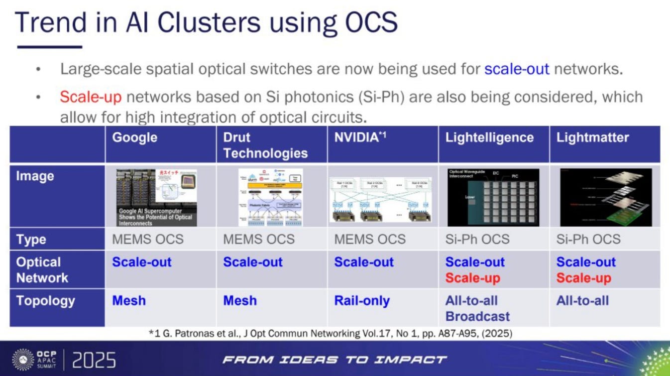
For OCS, the difficulty lies in assembly, alignment, reliability, and manufacturing cadence at high port counts. arXiv papers summarizing the advantages of MEMS-based OCS also stress that data-center economics require scaling to hundreds of ports, with weekly manufacturing and testing throughput at high volume—imposing much stricter requirements on design for manufacturability and reliability.
In short, while the demand side defines the direction of data rate and port count, the supply side ultimately determines the delivery curve and availability. During the transition from 800G to 1.6T, supply constraints may even reshape demand, for example by favoring more readily available device combinations or by introducing new speeds first at shorter, more controllable link distances.

2025年5月13日
OIO: From CPO to “In-Package Optical I/O,” and Its Key Components and Mass-Production Barriers
OIO is widely regarded as a “must-answer question” in the 2026–2028 timeframe for three core reasons:
First, shortening electrical paths delivers the largest system-level gains.
In its photonic switching platform announcements, NVIDIA presents multiple system-level metrics—such as fewer lasers, higher power efficiency and signal integrity, and improved network resilience—and positions them as next-generation networking solutions for hyperscale AI factories. While exact figures vary by implementation, the direction is clear: as data rates continue to rise, relying on long in-board electrical interconnects incurs increasingly high power and engineering costs.
Second, OIO requires platform-level process maturity to scale.
TSMC has publicly described its COUPE (Compact Universal Photonic Engine) roadmap: qualifying small pluggable form factors around 2025, then combining them with advanced packaging (e.g., CoWoS) around 2026 to bring optical connectivity directly into the package and drive CPO adoption. TSMC’s research materials emphasize EIC–PIC integration and reduced coupling loss as core COUPE design goals. This underscores that OIO is not about whether a single company can build a prototype, but whether a wafer manufacturing + opto-electronic co-design + packaging + coupling/connection + testing platform can achieve stable mass production.
Third, maintainability and reworkability are being actively redesigned—not passively sacrificed.
NVIDIA has disclosed an engineering architecture for its photonic switching solution based on optical subassemblies composed of multiple optical engines, a structure widely viewed as a key method to improve manufacturability and maintainability rather than accepting “non-serviceable” designs.

Key Components: From External Cabling to High-Precision Internal Optical Connections
One major difference between OIO/CPO and pluggable modules lies in how fibers connect to optical engines. Connections move from external rack-level cabling to dense, high-precision optical interconnects inside packages or at the board level, bringing the following components to the forefront:
High-density multi-fiber connectors:US Conec positions its MMC connectors as ultra-high-density multi-fiber solutions and explicitly identifies CPO/near-packaged optics as key application scenarios—once optical engines move closer to the ASIC, fibers must bridge between the engine and the board edge.
FAUs and fiber arrays:Browave has demonstrated fiber array units supporting high channel counts with micron-level pitch tolerance, highlighting their use in datacenter transceiver SIP assembly.
Optics closer to the chip:Corning, in public articles, explains the core CPO logic as co-packaging photonic chiplets/optical engines with ICs on a common substrate to shorten electrical paths, reduce power, and increase bandwidth density.
Ultimately, mass production of OIO hinges on three hard metrics: yield, testability, and maintainability. Broadcom has emphasized reliability and production-grade quality metrics in its CPO product launches, tied to validation with major cloud customers—signaling the industry’s shift from proof-of-concept to engineering for production-grade SLAs.

2025年11月29日
OCS: From Electrical Switching to the Optical Path Layer—and Why It Is Gaining Momentum in AI Clusters
OCS is not a new concept, but it has re-emerged as a focal point in AI clusters due to AI communication patterns. When data flows exhibit strong predictability and stability (e.g., driven by parallel strategies and collective communication), establishing end-to-end optical circuits can carry large volumes of inter-rack traffic with lower energy and lower forwarding latency, while avoiding repeated O–E–O conversions. Research analyses of Google TPU architectures identify OCS as a core element of all-optical networks, noting that MEMS-based solutions directly connect fiber to fiber to reduce O–E–O overhead, power consumption, and latency.
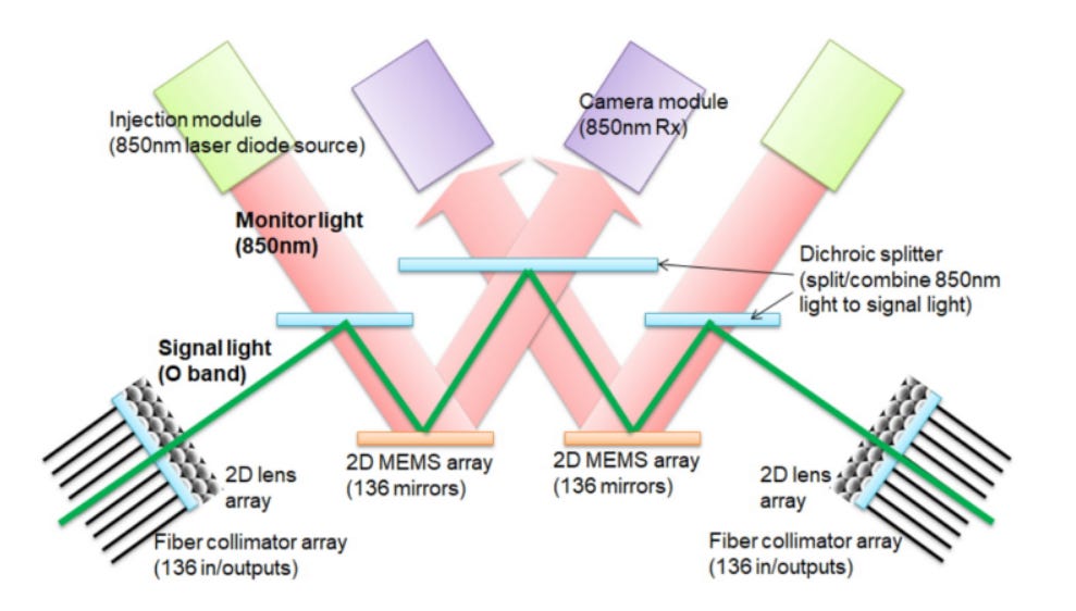
Technically, OCS is centered on reconfiguring optical paths rather than per-packet forwarding, leading to three typical advantages (using MEMS-based approaches as an example):
Low energy consumption:Because there is no per-packet processing, energy per bit can be significantly lower than electrical packet switching; MEMS mirrors also consume minimal power to maintain state.
Low latency:Added latency is largely limited to propagation delay and minimal additional processing, whereas electrical switches may introduce nanosecond-scale (or higher) forwarding delays per hop.
However, OCS is not a universal replacement. Its main limitation lies in reconfiguration time and the associated control and receiver initialization overhead. Early prototype work (e.g., Google’s Helios papers) shows that command processing, mirror reconfiguration, and receiver-side electronic initialization can together create millisecond-scale throughput dips. To approach the experience of pure electrical networks, these bottlenecks must be reduced or traffic patterns must be sufficiently stable. This explains why real-world deployments often adopt hybrid architectures: electrical switching for bursty, highly dynamic traffic, and OCS for stable, coarse-grained inter-pod flows.

2025年8月7日
Technology Paths and Engineering Challenges
At least three major OCS technology paths exist, each with distinct supply chains and engineering challenges:
MEMS micromirror–based OCS, currently the most mature and widely discussed approach. Polatis describes its 3D-MEMS technology as enabling free-space fiber-to-fiber interconnection via micromirror deflection. The OCS market is also evolving from single-customer, in-house projects to multi-vendor ecosystems. Cignal AI noted in late-2025 updates that OCS has expanded into a multi-vendor datacenter market, with Google reportedly deploying tens of thousands of OCS ports and transitioning from self-built systems to commercial solutions.
Beam-steering/free-space optical switching(e.g., piezoelectric-driven). Polatis also highlights beam-steering approaches that use piezo actuators to align fibers. These paths often optimize specific trade-offs (loss, port count, mechanical complexity) but still require high-precision calibration and long-term reliability.
Programmable integrated photonics / waveguide mesh approaches, which are more on-chip–centric. Articles in Optica describe programmable photonics and waveguide meshes as reconfigurable optical networks implemented on-chip. European companies such as iPronics emphasize programmable photonic switching for AI networks. While these approaches offer higher integration and potentially faster switching, they face challenges in insertion loss, thermal control, and process uniformity—making their scaling timeline dependent on platform maturity and system-level fault tolerance.
Industry Takeaway on OCS
The industrial value of OCS lies primarily at the system architecture level, not the individual device level. As AI clusters treat interconnects as a programmable resource pool, OCS introduces a new optical path layer that enables topology reconfiguration, fault bypass, and higher link utilization at lower energy cost. Its commercialization inflection point will depend on port scale, reconfiguration overhead, control software maturity, and the supply chain’s ability to deliver high-port-count OCS with consistent manufacturing cadence and reliability.
Global Supply Chain Landscape: Division of Roles Among Taiwan, Japan, the United States, Europe, and China in 800G/1.6T, OIO, and OCS
To truly connect demand, technology, and delivery, the global supply chain must be analyzed along three core axes: components, manufacturing, and systems. Below is a region-by-region, industry-research–oriented mapping of roles (excluding stock tickers and pricing).

2025年8月17日
Taiwan: A Central Hub for Wafer Manufacturing, Advanced Packaging, System ODM, and Passive Components
Taiwan plays a dual role in next-generation optical interconnects—as both a platform provider and a system engineering integrator.
On the platform side, TSMC has clearly articulated its roadmap combining COUPE with advanced packaging. The plan is to first qualify COUPE in pluggable or compact form factors, then introduce CoWoS and other advanced packaging to bring optical connectivity directly into the package, enabling CPO. This positions Taiwan as a process-platform center for OIO/CPO: regardless of where upstream photonic chips are designed, large-scale deployment ultimately depends on reusable manufacturing and packaging platforms based in Taiwan.
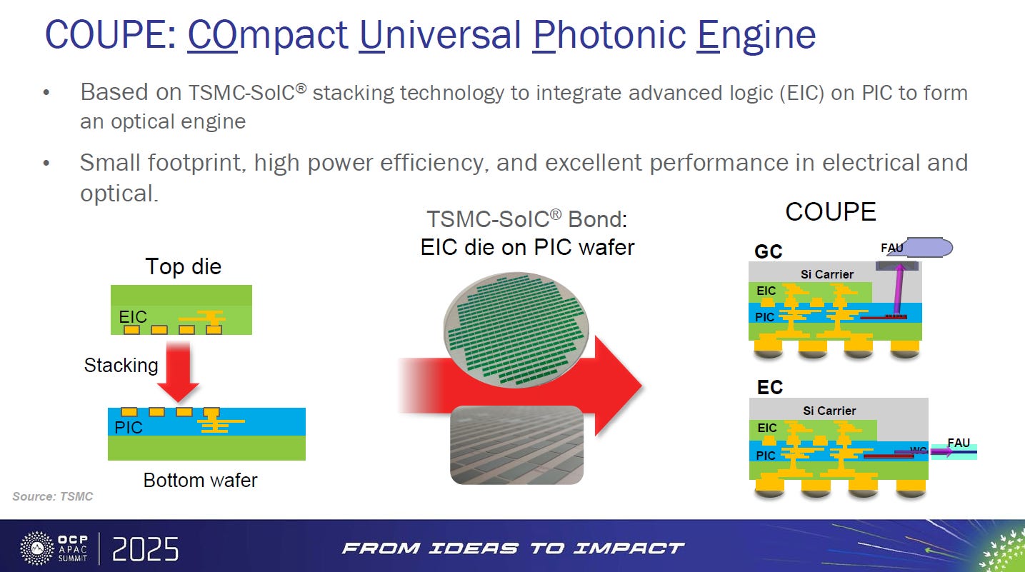
On the manufacturing and ecosystem side, NVIDIA has explicitly listed multiple key partners in its photonic switching ecosystem, including TSMC and major Taiwanese or regional players in manufacturing and passive components (such as Browave and SPIL). NVIDIA describes this ecosystem as a co-engineered integration of silicon, photonic processes, and the supply chain. SPIL, as an OSAT, has also been publicly cited as an important participant in NVIDIA-related AI chip packaging, underscoring the strategic importance of advanced packaging in AI–photonics convergence.

2月28日
In passive components, Browave has publicly disclosed its fiber-array capabilities, noting headquarters in Hsinchu, Taiwan, and manufacturing bases in mainland China. This reflects the cross-regional manufacturing footprint of fiber arrays and high-precision passive components. In OIO/CPO architectures, such passives shift from being optional parts to critical determinants of yield and serviceability.

2月26日
Japan: Long-Standing Strengths in High-Reliability Materials, Optical Devices, Connectors, and Precision Manufacturing
Japan has long excelled in high-reliability materials, optical devices, precision connectors, and manufacturing processes, capabilities that remain essential in the 800G/1.6T and OIO/CPO era.
Within the CPO/OIO ecosystem, NVIDIA’s photonic switching partner list includes key Japanese players such asSENKOandSumitomo Electric, highlighting Japan’s continued importance in connectors, fiber interconnects, and optical components. SENKO emphasizes the foundational role of connectors in network deployment and reliability; in CPO/OIO, connectors and high-density multi-fiber interconnects evolve from rack-level cabling issues into package-level and board-level assembly and maintenance challenges.


2025年6月10日
Japan also continues to invest heavily in semiconductor lasers and thermal management. Sumitomo Electric Industries highlights its long-term R&D and manufacturing experience in semiconductor lasers, noting that light sources are a key factor in high-bandwidth optical communications. In the 1.6T era, the value of InP-related capabilities lies not only in technical feasibility, but in the ability to scale capacity while maintaining consistency and reliability.
United States: System and Switch-Silicon Leadership, Key Optical Components, and the Most Active OCS Ecosystem
The United States exhibits a strong system- and standards-driven role in the transition to 800G/1.6T and next-generation optical interconnects. Network switch silicon and AI platform roadmaps define port speeds and deployment timing, while key optical component vendors, fiber/connectivity giants, and an active OCS startup ecosystem define supply-side boundaries.
On the system side,NVIDIAhas publicly introduced platforms such as Spectrum-X Photonics and Quantum-X Photonics, providing port configurations and delivery timelines (with Ethernet photonic switching products targeting 2026).Broadcomhas similarly emphasized progress in CPO switching products and production-grade reliability metrics, signaling that system-level engineering of switch silicon plus optical engines is entering a more mature phase.

2025年6月4日
On key components,Lumentum’s technical blogs highlight its growing mass-production capability for 200G/lane EMLs and capacity expansion to meet hyperscale demand—corroborating research findings that identify laser light sources as a bottleneck.Corninghas publicly explained the role of CPO in fiber connectivity and has been reported to expand fiber and connectivity production for AI data centers, reflecting how fiber and connectivity are becoming strategic infrastructure materials for AI.
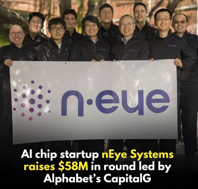
California-based startup nEye Systems has raised $58 million in a funding round led by CapitalG, Alphabet’s growth-stage fund. Backed by tech giants including Microsoft’s M12, Micron Technology, and NVIDIA, NEye is developing optical circuit switches—chips that transmit data using light instead of electricity, drastically cutting down energy consumption.
In the OCS ecosystem, the U.S. has the richest academia–industry pipeline. Early Google Helios prototype papers defined reconfiguration bottlenecks and hardware requirements for data-center OCS, establishing core engineering challenges. Papers further analyzed MEMS-based OCS from scalability and manufacturability perspectives. In parallel, startups supported by capital and supply chains are advancing new optical switching technologies. Industry media reportnEye Systemsas an academically rooted, well-funded optical switching startup—illustrating OCS’s transition from single-vendor internal projects to broader industrial competition.

2月26日

2月20日

1月29日
Europe: Stronger Momentum in OCS and Programmable Photonics, Supported by MEMS and Optical Manufacturing
Europe’s most distinctive contributions to next-generation optical interconnects lie in OCS, programmable photonics, and strong MEMS and optical manufacturing and research infrastructures, supporting technological diversity.
In commercial OCS,HUBER+SUHNER (Polatis)provides data-center optical circuit switching products and publicly discloses port-scale coverage, indicating real progress in high-port-count OCS commercialization. Company announcements around capacity expansion and orders further suggest a transition from pilot deployments to broader-scale supply.
In programmable photonics and waveguide-mesh approaches,iPronicspositions itself around AI networking and programmable photonic switching, with operations based in Valencia, Spain. This path relies heavily on integrated photonics process uniformity, thermal control, insertion-loss management, and deep coupling with system software orchestration.
In MEMS manufacturing,Silex Microsystemsdescribes its experience as a MEMS foundry producing micromirror components for optical communications, with facilities in Stockholm, Sweden. For OCS, cross-regional coordination among MEMS fabrication, system assembly, and integration determines whether port counts can scale while maintaining yield and consistency.


2025年11月12日
China: Strength in Large-Scale Optical Module Manufacturing, Expanding Toward Components and System Co-Design
China’s primary advantage in the 800G/1.6T era lies in large-scale optical module manufacturing and delivery, with its role expanding from “module assembly” toward participation in key components and system architecture co-design, including silicon photonics and OCS-related chains.
On the demand side, LightCounting reports indicate that large-scale deployment of 800G transceivers is expected in China during 2026–2027, followed by 1.6T/3.2T. Even without overseas demand, domestic AI cluster construction alone is sufficient to sustain strong 800G demand over an extended period.
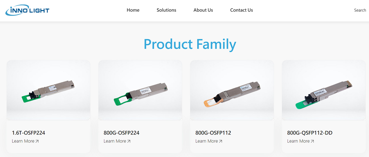
On the supply side, research firms identifyInnolightandEoptolinkas major datacom module suppliers and emphasize the importance of upstream optical component sources in market expansion. Further analyses of Google-related high-spec optical module demand note that the supply capacity and customer collaboration of suppliers such as Innolight and Eoptolink can materially influence deployment pace.

More structurally, China’s opportunity lies in moments of global bottlenecks—particularly in lasers and other critical components—where alternative supply and engineering capabilities toward higher integration (silicon photonics, optical engines) become competitive differentiators. Laser shortages and extended lead times are pushing the industry to seek second sources and substitutes, reshaping competitive dynamics in the laser supply chain. Such shifts often accelerate the industrialization of new device routes, including broader silicon photonics adoption and more supply-resilient light-source combinations.
Thanks for reading SEMIVISION @_@! This post is public so feel free to share it.


PreviousNext
TopLatestDiscussions








See all