A Half-Century Odyssey in Semiconductors: Kinam Kim's Samsung Journey of Innovation and Insight
A Half-Century Odyssey in Semiconductors: Kinam Kim's Samsung Journey of Innovation and Insight
- Source: SemiVision
- Author: SEMIVISION
- Published: 2026-03-02T21:34:10+08:00
- URL: https://tspasemiconductor.substack.com/p/a-half-century-odyssey-in-semiconductors (1) A Half-Century Odyssey in Semiconductors: Kinam Kim's Samsung Journey of Innovation and Insight


A Half-Century Odyssey in Semiconductors: Kinam Kim's Samsung Journey of Innovation and Insight
Original Article By SemiVision Research [Reading time: 20 mins]

Mar 02, 2026
∙ Paid
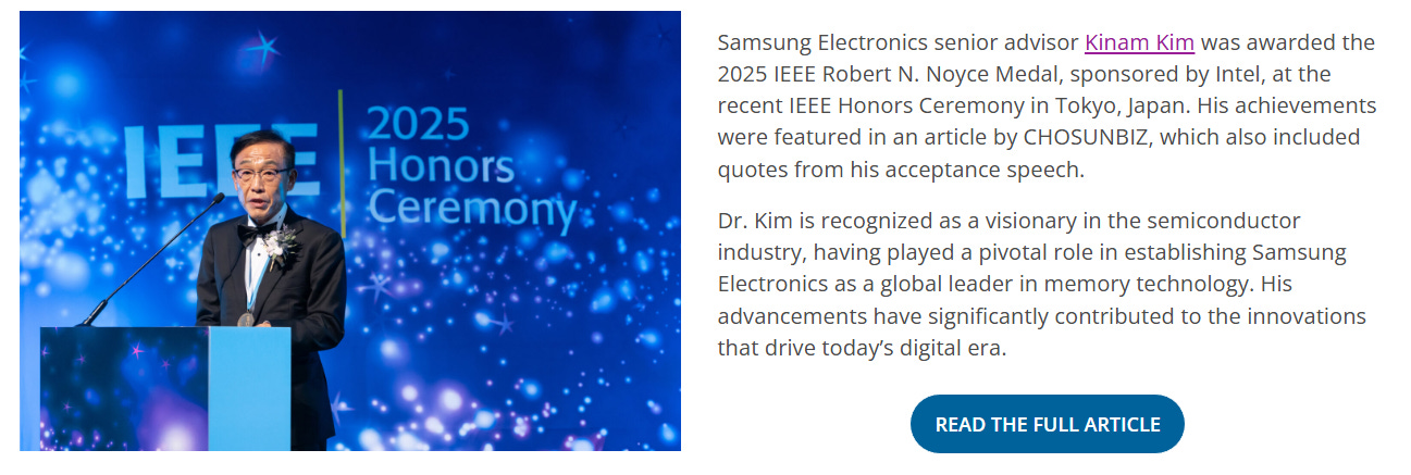
In a distinguished talk delivered at the ISSCC Solid-State Circuits Symposium event,Dr. Kinam Kim, Senior Advisor and former CEO of Samsung Electronics, reflected on nearly five decades of pioneering work in the semiconductor industry. With humility and passion, he shared his personal story, key technical breakthroughs, and timeless lessons for future engineers.
Titled “My Half-Century Journey of Semiconductor Innovation: Key Contributions, Lessons Learned and Insights for Future Engineers,” the presentation wove together autobiography, technical depth, and forward-looking vision. Kim expressed deep gratitude to ISSCC for the invitation and emphasized how semiconductors have been the quiet engine driving humanity toward greater convenience and prosperity—from the personal computer era through mobile computing to the current explosion of artificial intelligence
From Student to Semiconductor Pioneer
Kim’s path into semiconductors began in 1977 when he enrolled in the College of Electrical Engineering at Seoul National University. Upon graduation, while many classmates pursued advanced degrees, academic careers, or roles at research institutes, Kim felt drawn to the fast-paced, dynamic world of private industry. In 1981, he was selected as a Samsung Electronics industrial scholarship student and joined the company’s semiconductor manufacturing technology team.
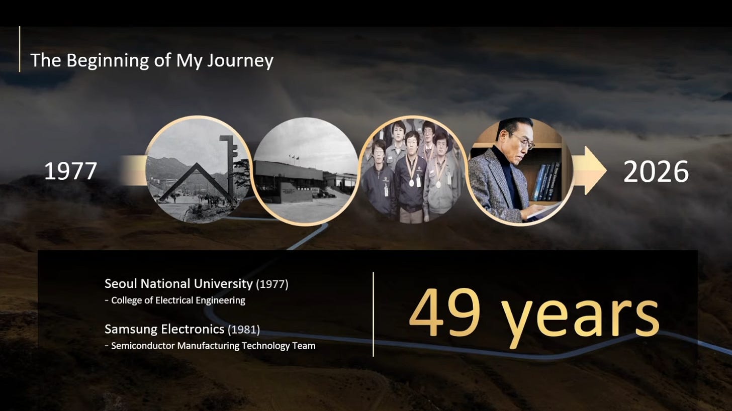
The early years were filled with formidable challenges—technical hurdles, resource constraints, and the pressure to innovate in a rapidly evolving field. Yet Kim remained steadfast, crediting the unwavering support of colleagues, friends, and mentors for his longevity and success. Now a 49-year veteran (approaching half a century by the time of the talk), he looked back and recognized the immense potential he had sensed early on: semiconductors could transform lives and societies. This conviction fueled his commitment, turning a career choice into a lifelong mission to contribute to a better world.
The Relentless March of Semiconductor Scaling
Since the 1970s, the commercialization of ever-smaller, faster transistors has been the cornerstone of electronics progress. High-density integration and speed improvements have shrunk device form factors while boosting performance, enabling the PC revolution, the mobile era, and now the AI age. Over the past 50 years, countless technologies have emerged, but Kim chose to highlight four transformative contributions in which he played a pivotal role: the Recessed Channel Array Transistor (RCAT) for DRAM, 3D Vertical NAND (V-NAND) flash, High Bandwidth Memory (HBM), and the Multi-Bridge Channel FET (MBCFET), also known as Gate-All-Around (GAA) technology.
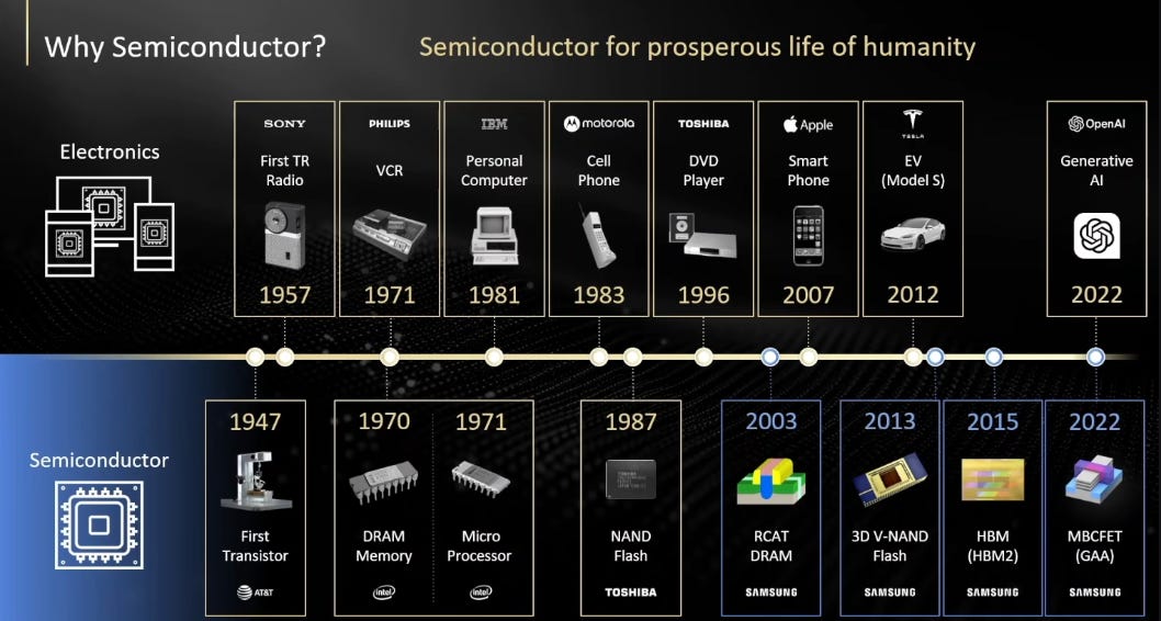
These innovations addressed fundamental scaling limits—short-channel effects, leakage currents, cell interference, and power-performance trade-offs—pushing the boundaries of what silicon could achieve.
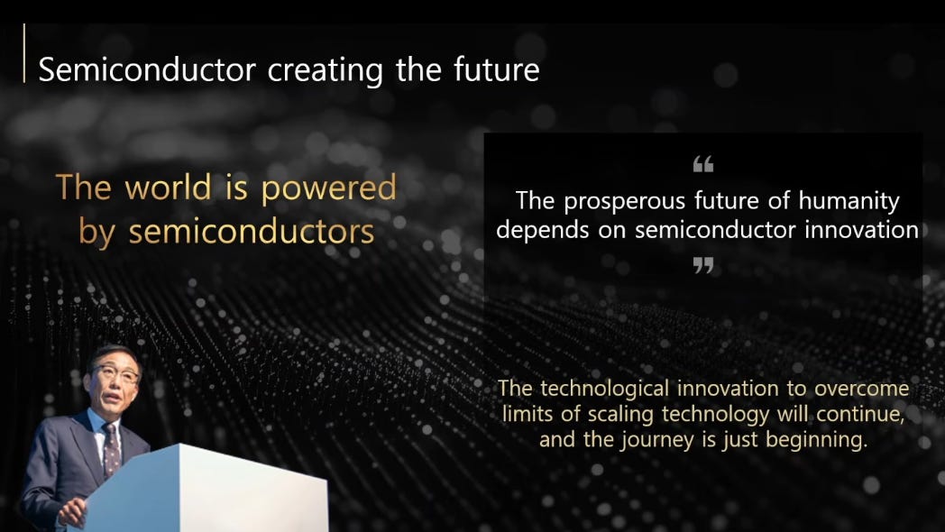
Semiconductor Creating the Future: Dr. Kinam Kim’s Vision and SemiVision’s Call to the Next Generation
The semiconductor industry is not just building chips—it is building the future of humanity. In a powerful presentation captured in these slides, Dr. Kinam Kim, former CEO of Samsung Electronics and one of the most influential figures in modern memory and logic technology, delivers a clear and inspiring message:
“The world is powered by semiconductors.”
“The prosperous future of humanity depends on semiconductor innovation.”
Set against a mesmerizing backdrop of glowing circuits resembling a digital universe, these words carry profound weight. Dr. Kim reminds us that every leap forward—from PCs to smartphones, from cloud computing to today’s explosive growth in artificial intelligence—has been made possible by relentless innovation in silicon. And as he stands on stage under dramatic lighting, he leaves no doubt:
“The technological innovation to overcome limits of scaling technology will continue, and the journey is just beginning.”
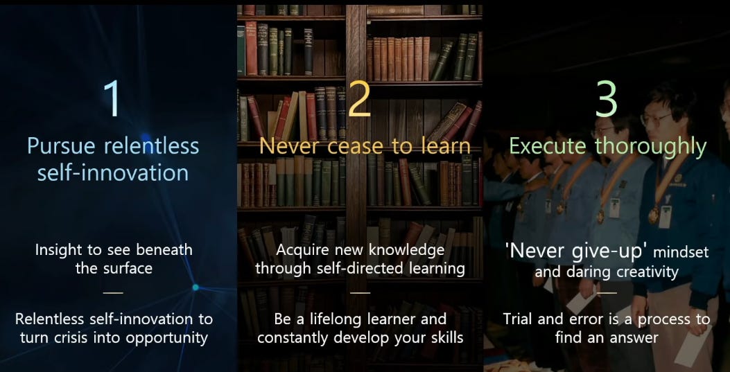
Three Pillars That Define a Lifetime of Impact
Dr. Kim distills nearly 50 years of experience into three timeless principles, beautifully illustrated in the slides:
Pursue Relentless Self-Innovation
True breakthroughs come from looking beneath the surface. When scaling walls appeared insurmountable, Kim and his teams turned crises into opportunities—RCAT for DRAM, 3D V-NAND, HBM, and the invention of Multi-Bridge Channel FET (Gate-All-Around) two decades before mass production. Insight transforms problems into progress.
Never Cease to Learn
Even after decades at the top, Dr. Kim continues to read the latest papers, track emerging trends, and stay ahead of one of the fastest-moving fields in technology. Lifelong learning is not optional—it is the foundation of sustained excellence.
Execute Thoroughly
Nearly 40 years ago, when many said it was impossible, Kim’s team developed Korea’s first 1Mbit DRAM. That moment forged a “never give-up” mindset: push forward with daring creativity and rigorous execution until physics itself says stop.
These three pillars—self-innovation, continuous learning, and thorough execution—are not just lessons from the past; they are the roadmap for the next wave of semiconductor engineers.
SemiVision’s Perspective: A Strong Call to Learn More, Learn Deeper, Learn Now
As someone who has followed the semiconductor industry closely for years, I want to add one clear and urgent message inspired by Dr. Kim’s talk:The single most powerful action any young engineer, student, or professional can take right now is to dramatically increase the depth and breadth of their learning.The pace of change in semiconductors has never been faster:
2nm-class logic is already in production
Gate-All-Around (GAA / MBCFET / nanosheet) is the new mainstream
HBM3E / HBM4 is fueling the AI boom
3D stacking, backside power delivery, CFET, silicon photonics, and co-packaged optics are moving from research to reality
New memory types (CXL memory pooling, compute-in-memory, ferroelectric, etc.) are emerging
The entire ecosystem—from materials to EDA tools, from packaging to system architecture—is being reinvented simultaneously
This is not a time to coast on yesterday’s knowledge.This is the moment to:
Read the latest IEDM, VLSI Symposium, ISSCC, and ECTC papers (not summaries—original papers)
Study actual process flows, transistor physics, interconnect challenges, thermal/power walls
Learn 3D-IC design, advanced packaging, backside power delivery network (BS-PDN)
Understand the physics and economics behind DRAM scaling limits, NAND layer stacking, and logic node transitions
Follow foundry roadmaps (Samsung, TSMC, Intel), memory leaders (Samsung, SK hynix, Micron), and AI accelerator trends (NVIDIA, AMD, OpenAI, Grok/xAI, etc.)
Master simulation tools, parasitic extraction, reliability physics, and yield analysis—not just high-level concepts
Dr. Kim himself is still studying new papers after 50 years. That should be our signal.
SemiVision’s encouragement to everyone reading this:
Don’t wait for someone to teach you.
Don’t wait for the “right” course or the “perfect” job.
Start today. Read one more paper this week. Understand one more process challenge. Ask harder questions. Dig deeper.
The people who will define the 2030–2040 semiconductor era are the ones who are learning the most aggressively right now—in 2026.
The journey is just beginning, and the brightest chapters are still unwritten.But they will be written by those who refuse to stop learning.
Let Dr. Kinam Kim’s example—and his three pillars—inspire you.And let this be SemiVision’s direct message to the next generation:
Learn more. Learn deeper. Learn now.
The future of humanity really does depend on it.

1月19日
Below we will share:
Breakthrough 1: RCAT – Pioneering 3D Transistors in DRAM
Breakthrough 2: 3D Vertical NAND – Revolutionizing Flash Storage
Breakthrough 3: High Bandwidth Memory (HBM) – Fueling AI Performance
Breakthrough 4: MBCFET (Gate-All-Around) – The Next Frontier in Logic
Samsung Keynote from SEMICON KOREA 2026
Breakthrough 1: RCAT – Pioneering 3D Transistors in DRAM
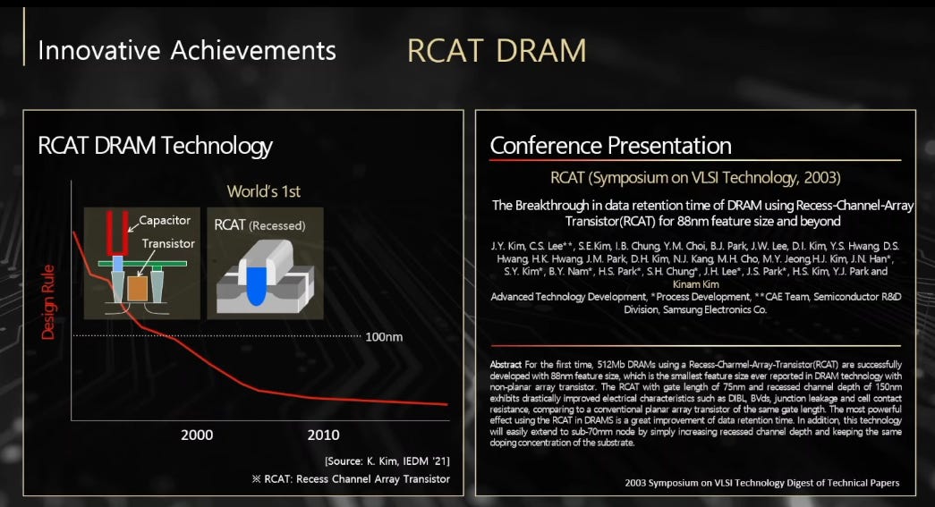
In the early 2000s, conventional planar transistors in DRAM cells hit a scaling wall below 100 nanometers. Each memory bit relies on a classic 1T-1C (one transistor, one capacitor) structure, but aggressive shrinking of planar designs exacerbated short-channel effects, leading to unacceptable off-state leakage, degraded data retention, and reliability issues. The industry urgently needed a solution that extended channel length for better gate control without requiring radical process overhauls or skyrocketing costs.
Under leadership including key figures like Kim (notably contributions from teams at Samsung, including Joonsuk Kim, Kinam Kim, and others), extensive exploration of transistor candidates culminated in a pivotal innovation: the Recessed Channel Array Transistor (RCAT). This design recesses the channel into a U-shaped trench etched into the silicon substrate, effectively lengthening the effective channel path within the same 2D footprint. The longer channel path dramatically suppresses short-channel effects, improves subthreshold swing, reduces leakage, and boosts data retention time—often doubling refresh intervals—while maintaining compatibility with existing planar DRAM flows.
Key technical challenges included achieving uniform gate oxide quality on the curved, recessed silicon surface, which exhibits varying crystal orientations (e.g., (100) on top vs. (111) on sidewalls). This complicated traditional thermal oxidation, requiring optimized processes to avoid defects and ensure reliable gate dielectric integrity. Despite initial industry skepticism about manufacturability and yield at scale, the RCAT proved robust.
Samsung pioneered RCAT, first presenting it at the 2003 VLSI Technology Symposium (with foundational work also highlighted at IEDM conferences). The breakthrough enabled continued scaling: Samsung successfully developed and mass-produced 512 Mb DRAMs using RCAT at 88 nm feature size, marking the world’s first mass-produced 3D transistor in the silicon industry. By 2004–2005, RCAT was deployed in production at 90 nm nodes, and refinements like the spherical recessed variant (S-RCAT) extended it to sub-70 nm (e.g., 60 nm mass production in 2007). This allowed DRAM to push into the 10 nm regime without abandoning the 1T-1C architecture.

RCAT’s impact was profound and enduring. It became the foundational access transistor architecture for modern DRAM cells, evolving through iterations like saddle fin or fin-like enhancements while retaining the recessed-channel core. Competitors (SK Hynix, Micron) adopted similar recessed or 3D channel concepts, making RCAT-style transistors ubiquitous in today’s high-density commodity DRAM (DDR5, LPDDR5X), graphics memory (GDDR), and even early HBM generations.
As of early 2026, the DRAM industry remains anchored in planar (or quasi-planar) RCAT-derived transistors for most production nodes (around D1c/D1γ or 10–12 nm class). However, the relentless push for density—driven by AI workloads demanding massive memory capacities—has exposed the limits of 2D scaling in 6F² cell layouts. Leakage, capacitor aspect ratio challenges, and bitline coupling are intensifying.
The next major evolution is underway: transition to vertical channel transistors (VCT) or vertical gate (VG) architectures, often paired with a shift to denser 4F² cell layouts (reducing area by ~30% theoretically). Samsung plans early VCT-based 3D DRAM introductions in 2025, with prototypes and electrical demos from Samsung, SK Hynix, and others accelerating. Samsung’s VS-CAT (Vertically Stacked Cell Array Transistor) or similar vertical stacking approaches target sub-10 nm nodes (D1d/0a generations by 2027–2028), potentially enabling true multi-layer 3D DRAM in the late 2020s/early 2030s—mirroring NAND’s vertical revolution but adapted for volatile DRAM cells.
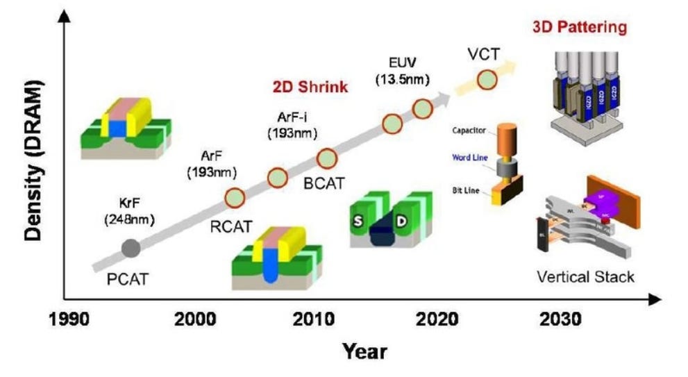
Source: Samsung 2025
This trajectory underscores RCAT’s legacy: it bought two decades of scaling headroom, but AI-driven demand is forcing a paradigm shift toward vertical/3D structures. Industry roadmaps point to VCT/4F² as the bridge to full 3D DRAM, promising higher densities (e.g., 48–96 Gb+ dies), better power efficiency, and sustained cost-per-bit reductions. Meanwhile, ongoing refinements in EUV lithography, high-k/metal-gate peripherals, and capacitor materials (e.g., taller pillars) extend RCAT-based nodes through the mid-to-late 2020s.
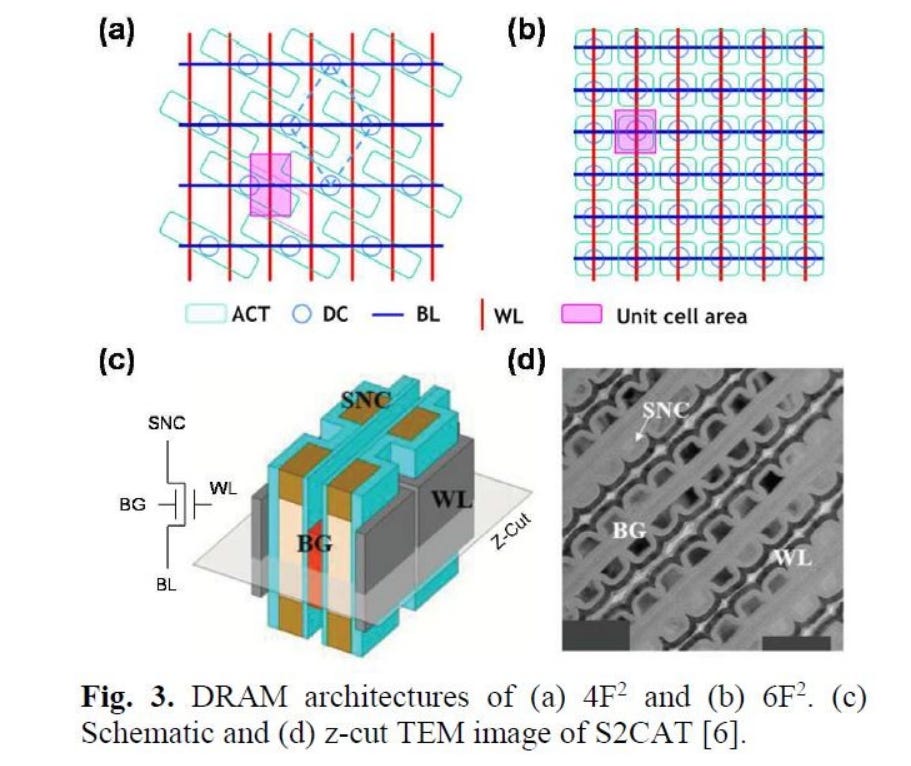
In summary, RCAT was the breakthrough that pioneered 3D transistor concepts in high-volume silicon manufacturing, enabling DRAM’s dominance in cost-sensitive, high-capacity applications. Its principles continue to influence the industry’s path toward vertical scaling, ensuring memory keeps pace with the exploding compute demands of the AI era.

Breakthrough 2: 3D Vertical NAND – Revolutionizing Flash Storage
For NAND flash, used in mass data storage, the early 2000s brought similar scaling crises. Planar floating-gate transistors could not reliably shrink below 20 nanometers due to cell-to-cell interference, high programming voltages, leakage, and narrowing process windows.The team shifted to silicon nitride as a charge-trap material, replacing floating gates. Charge Trap Flash (CTF) offered discrete trap sites inherently resistant to leakage and less vulnerable to interference, allowing thinner structures and shorter channels. Combining CTF with vertical transistor stacking—using technologies like Silicon Reactor Gate (SRG)—took nearly a decade of relentless development.
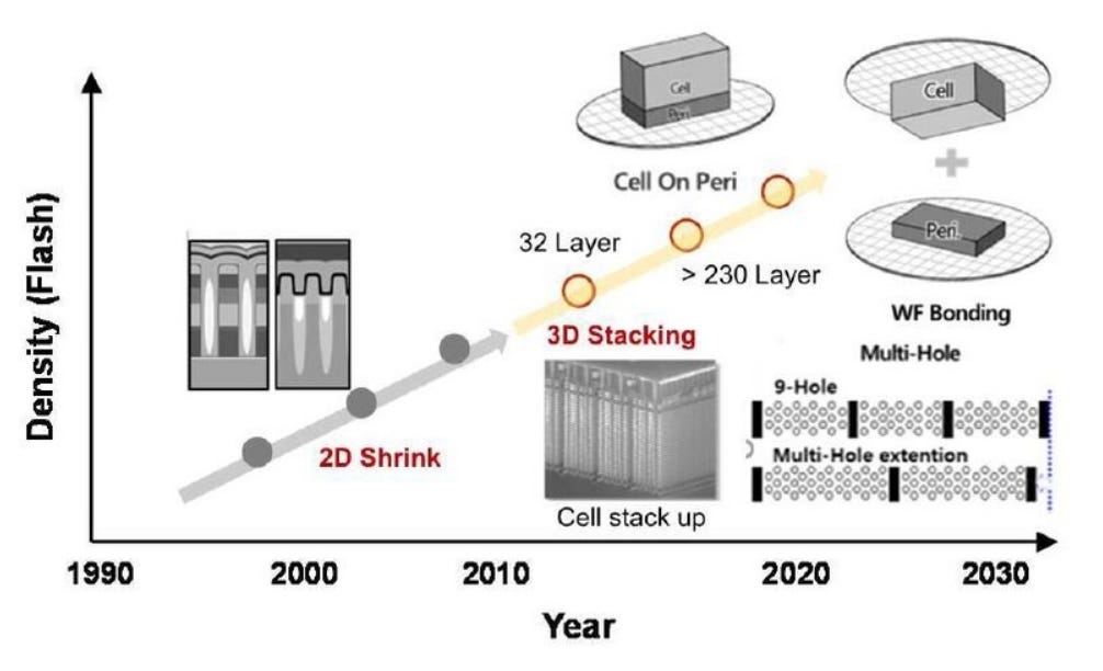
In 2013, Samsung achieved the world’s first mass production of 24-layer 3D Vertical NAND. This landmark shifted the NAND industry from 2D to 3D scaling, dramatically increasing bit density and reducing cost per bit. CTF-based 3D V-NAND has since become the standard, powering the explosive growth of SSDs, smartphones, data centers, and cloud storage.
Samsung’s pioneering V-NAND, introduced after over a decade of research, utilized a proprietary vertical interconnect process with etched holes connecting up to 24 cell layers electronically. This breakthrough not only overcame 2D scaling limits but also enabled multi-level cell (MLC) and later triple-level cell (TLC) and quad-level cell (QLC) implementations for higher capacities at lower costs per bit. By 2014, Samsung advanced to 32-layer 3-bit MLC V-NAND, further solidifying leadership.
Competitors quickly followed: Micron and Intel introduced their own 3D NAND architectures, SK hynix adopted a 4D PUC (Punch-up Cell) structure, Kioxia/Western Digital developed BiCS FLASH, and China’s YMTC leveraged Xtacking hybrid bonding. These innovations accelerated layer stacking, with the industry progressing from sub-100 layers in the mid-2010s to over 200 layers by the early 2020s.
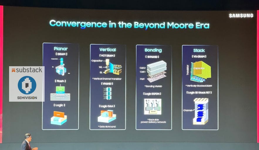
As of early 2026, the 3D NAND landscape features aggressive layer scaling to meet surging demand:
Samsung’s 9th-generation V-NAND reaches 286 layers (with QLC variants), delivering up to 50% higher density and samples shipped to major clients like Google and Apple for AI data centers and smartphones.
SK hynix leads in production with 321-layer V9 samples, targeting ultra-high-capacity enterprise SSDs for AI, emphasizing energy efficiency and performance.
Micron’s offerings hit around 276 layers, focusing on endurance improvements for automotive and enterprise.
Kioxia/Western Digital’s BiCS8 is at 218-232 layers, with BiCS10 (332 layers) production expedited to 2026 for high-capacity AI/hyperscale storage, promising 59% bit density gains via CBA (CMOS Bonded to Array) architecture.
YMTC advances with 270-300 layers, narrowing the gap despite geopolitical challenges.
The industry roadmap points to 400+ layers imminently—Samsung develops 400-plus-layer 10th-gen V-NAND (potentially skipping 300-layer nodes), SK hynix eyes 370-400 layers, and long-term visions include 500+ layers by 2027 and 1000+ by 2030. These leaps rely on innovations like hybrid bonding, ultra-low temperature etching, and advanced channel hole etching to manage aspect ratios exceeding 100:1 while maintaining yield.
Broader trends highlight 3D NAND’s pivotal role in the AI era. The global 3D NAND market, valued at around USD 25-30 billion in 2025, is projected to grow rapidly (CAGR 20-26%) toward USD 70-190 billion by the early 2030s, driven by AI training/inference clusters demanding massive NVMe SSD pools for data lakes and checkpoints. AI data centers have shifted demand toward high-capacity enterprise/QLC NAND, causing structural shortages: NAND prices surged 40-100%+ in late 2025-2026, with hyperscalers pre-buying output and some foundries demanding multi-year upfront payments. Consumer electronics face rationing, potentially halting smaller firms as capacity prioritizes AI servers.
QLC adoption accelerates for cost-per-bit reduction (now mainstream in enterprise), while endurance enhancements and PCIe 5.0/6.0 interfaces support faster throughput. However, supply constraints—prioritization of high-margin HBM/DRAM by top players (Samsung, SK hynix, Micron)—exacerbate tightness, with experts warning of decade-long shortages amid unchecked AI growth.
Overall, 3D V-NAND sustains Moore’s Law for storage, enabling exabyte-scale AI infrastructure, edge computing, 5G/IoT, and automotive autonomy. The “layer race” defines competitiveness through 2030, with cost/bit continuing to plummet and density soaring to handle the data deluge from generative AI and hyperscale clouds.

Breakthrough 3: High Bandwidth Memory (HBM) – Fueling AI Performance
As applications like AI demanded exponentially higher memory bandwidth, traditional solutions like DDR fell short in delivering the massive parallel data throughput needed for training and inference on large-scale models. HBM addressed this bottleneck through innovative 3D stacking technology, utilizing Through-Silicon Via (TSV) interconnects to vertically integrate multiple DRAM dies with a logic base die. This architecture enables wide, high-speed interfaces (typically 1024-bit or more) directly between the processor and memory stack, achieving terabytes-per-second bandwidth while reducing latency and power consumption compared to off-package solutions.
JEDEC standardized HBM in 2013, with key contributions from Samsung, SK Hynix, and AMD. Under leadership including key figures like Kim at Samsung, the company developed and mass-produced HBM2 in 2015. Initially adopted for high-end graphics processing units (GPUs) and high-performance computing (HPC), HBM quickly evolved into the go-to high-bandwidth solution for AI accelerators. Its ability to deliver terabytes-per-second bandwidth has become indispensable for handling the enormous datasets and parameter counts in modern large language models (LLMs) and generative AI workloads.
Since then, the HBM landscape has accelerated dramatically, driven by the explosive growth of AI infrastructure. From HBM2E (up to ~307 GB/s per stack) in the late 2010s, the industry advanced to HBM3 (around 460–819 GB/s) by 2022–2023, and then to HBM3E (reaching 1.2 TB/s per stack with speeds up to 9.8 Gbps and capacities of 24–36 GB per stack, often in 8–12Hi configurations) starting in 2024. These generations have powered flagship AI platforms, including NVIDIA’s Blackwell series and AMD’s Instinct accelerators.
Looking at recent and current trends (as of early 2026), the HBM market is experiencing unprecedented expansion. Global HBM revenues have surged, with estimates showing growth from around $17 billion in 2024 to roughly double that in 2025, and projections indicating a compound annual growth rate (CAGR) of 25–33% through the late 2020s. Market forecasts vary, but many analysts project the sector reaching $30–50 billion or more by the early 2030s, potentially capturing 40–50% of total DRAM revenue by 2030. This boom is fueled by hyperscalers (e.g., Microsoft, Google, Meta) aggressively building AI data centers, where HBM attach rates per GPU have skyrocketed to support trillion-parameter models.
Key market dynamics include intense competition among the big three suppliers: SK Hynix (long-time leader with ~50–60% share in recent quarters), Samsung (recovering strongly with HBM3E/HBM4 breakthroughs and aiming to reclaim ground), and Micron (gaining traction with advanced 12Hi/36GB products). In 2025, SK Hynix dominated HBM3E supply for major clients like NVIDIA, but Samsung made significant strides in yield improvements and secured key deals, narrowing the gap.
The most transformative shift is the transition to HBM4, with JEDEC specifications released in 2025. HBM4 doubles the interface width to 2048 bits, enabling bandwidths of ≥2 TB/s per stack (with pin speeds starting at 6.4 Gbps and scaling higher in variants like HBM4E). Stacks are moving toward 12–16Hi configurations with capacities up to 48 GB or more. Mass production ramped in late 2025/early 2026, positioning HBM4 as the standard for next-gen AI processors (e.g., NVIDIA’s Rubin, AMD’s MI400 series). This architectural leap supports even larger models while improving power efficiency and integration via advanced packaging like CoWoS and chiplets.
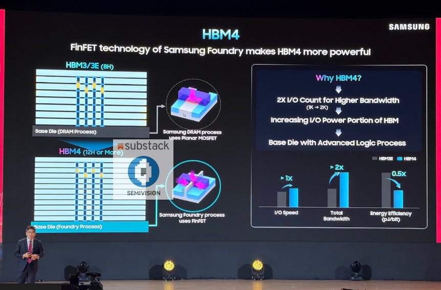
However, this rapid evolution has created supply constraints. AI demand has outpaced capacity, leading to widespread shortages. Manufacturers have reallocated wafer starts toward high-margin HBM (often requiring 3x more resources than standard DRAM due to TSV complexity and yields), starving supply for commodity DRAM, DDR5, and other segments. This has driven DRAM prices up sharply (some reports of 50–90% surges in quarters), extended lead times beyond a year for advanced products, and created ripple effects across consumer electronics, smartphones, PCs, and automotive sectors. Hyperscalers are hoarding HBM, with some forecasts indicating HBM could consume 20–23% of total DRAM wafer output in 2026 (up from prior years), and demand growing 70% YoY in some estimates.
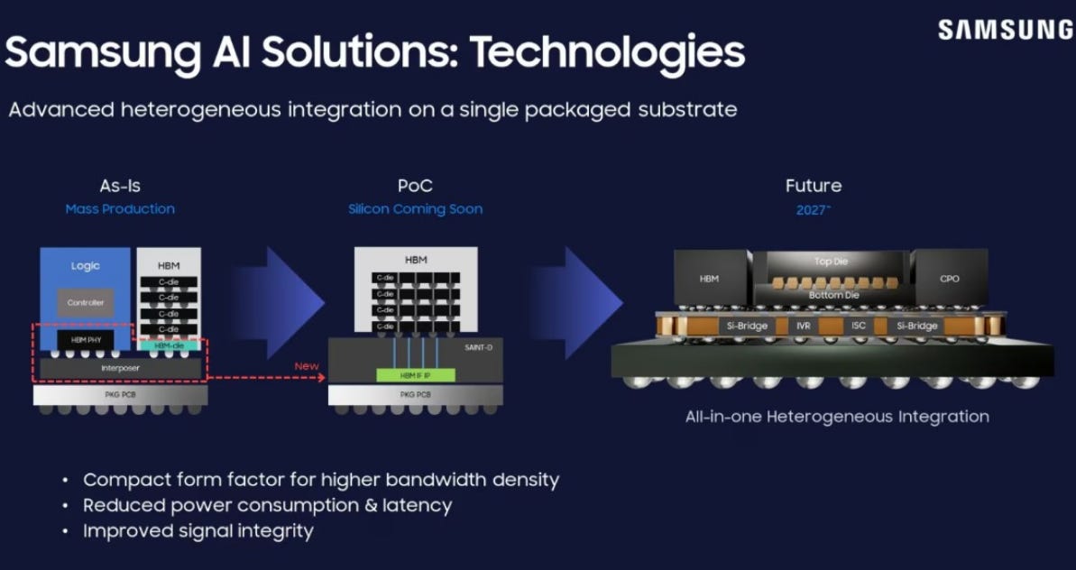
Looking ahead, the shortage is expected to persist through 2026–2027, though disciplined capacity expansions (new fabs, TSV yield optimizations, hybrid bonding for future stacks) and HBM4/HBM4E ramps should gradually ease pressure. Innovations like processing-in-memory (PIM) variants and even higher stacks promise continued performance leaps, solidifying HBM’s role as the critical enabler of the AI era. In essence, HBM has transitioned from a niche graphics solution to the foundational fuel powering the AI revolution, with its trajectory poised to reshape the entire memory and computing landscape for years to come.

2月13日
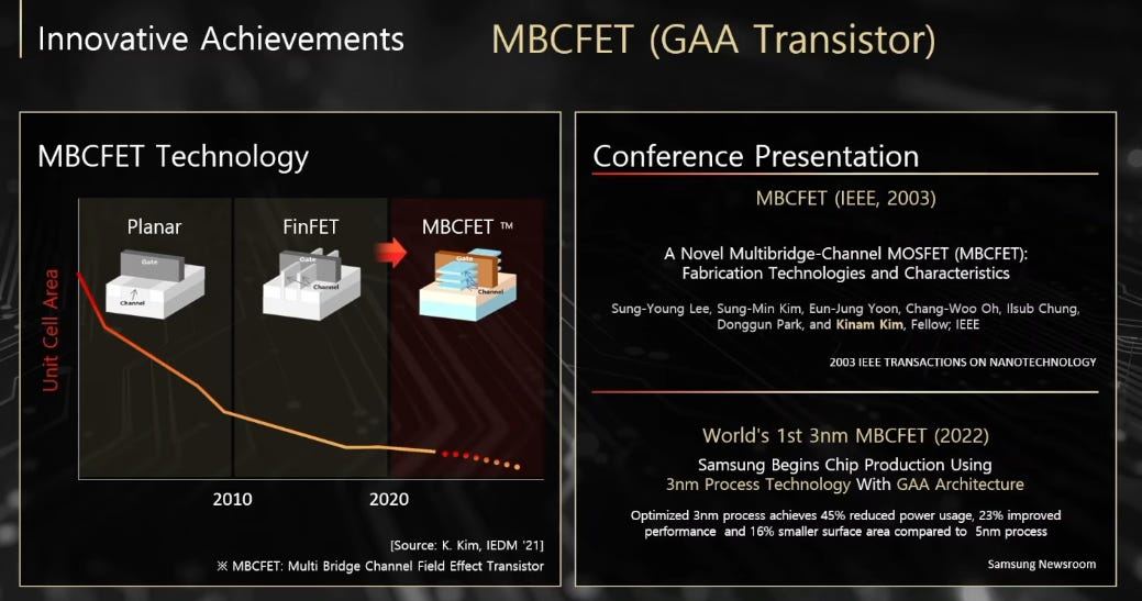
Breakthrough 4: MBCFET (Gate-All-Around) – The Next Frontier in Logic
FinFETs extended scaling beyond planar transistors by wrapping the gate on three sides of vertical fins, but limits emerged in the sub-5nm regime. The logical progression was Gate-All-Around (GAA), where the gate fully surrounds nanosheet or nanowire channels on all four sides, maximizing electrostatic control and drive current.

Source: Samsung
Samsung’s MBCFET (Multi-Bridge Channel FET) achieves this by stacking multiple horizontal channel layers. Drive strength scales simply by adding layers, offering flexibility in power-performance-area optimization. Kim’s team invented the core “Multi-Bridge Channel” concept around 2003, publishing fabrication details and characteristics that year. Samsung pioneered commercial adoption of GAA with its 3nm SF3 process in 2022, marking the first mass production of MBCFET transistors, which enabled up to 30% higher performance or 50% lower power compared to prior 5nm nodes.
By 2023, Samsung showcased enhanced SRAM design flexibility in its 3nm MBCFET at industry events, emphasizing its advantages for high-performance computing (HPC), AI, and mobile applications.
As of early 2026, Samsung continues to refine MBCFET for its 2nm SF2 node, focusing on better power efficiency and performance scaling through nanosheet widening, while collaborating with ecosystem partners to streamline design and verification for broader adoption.
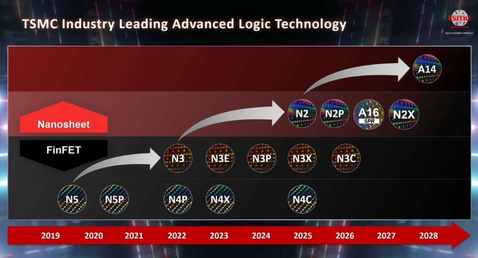
TSMC, the leading foundry, has transitioned to GAA with its nanosheet-based architecture in the N2 (2nm) node, starting volume production in late 2025.
This shift promises 10-15% speed gains or 25-30% power savings over previous generations, with a transistor density reaching 236.17 million per mm², making it ideal for AI/ML, 5G/6G, and HPC workloads.TSMC’s N2P variant incorporates backside power delivery (BSPDN) to further decouple power and signal lines, enhancing efficiency without altering the core GAA structure.
With over 15 customers already designing for N2, full commercialization is slated for the second half of 2026, solidifying TSMC’s dominance in advanced nodes amid strong AI-driven demand.

2025年5月9日
Intel’s approach features RibbonFET, its proprietary GAA implementation using stacked nanoribbons, debuting in the 18A (1.8nm-class) process targeted for 2025 production ramps and full volume by 2026.

Combined with PowerVia (backside power delivery), it delivers 25% performance uplift or 36% power reduction compared to prior nodes, addressing leakage and short-channel effects critical for sub-2nm scaling. Intel is hedging by ordering 2nm tiles from TSMC for next-gen CPUs to ensure timelines, while primarily using 18A internally for its own products like high-end processors.

2025年5月1日
Broader trends underscore GAA’s role in sustaining Moore’s Law amid AI and edge computing booms. The global GAA transistor market, valued at USD 600 million in 2024, is projected to reach USD 2 billion by 2034 at a 12.8% CAGR, driven by foundries like Samsung, TSMC, and Intel shifting from FinFET for better energy efficiency and density in 2nm and below.
Key enablers include High-NA EUV lithography for sub-2nm patterning, with Intel and TSMC adopting it for 2026 volume production.However, challenges persist: AI-led demand strains HBM supply and advanced packaging (e.g., CoWoS), turning backend processes into growth bottlenecks. Geopolitical reshoring, with U.S. investments exceeding USD 30 billion in TSMC, Intel, and Samsung, further accelerates innovation but heightens supply chain tensions.
Overall, GAA variants like MBCFET, nanosheet, and RibbonFET are pivotal for applications in autonomous vehicles, 5G/6G, and quantum-optimized computing, with the “2nm race” defining industry leadership through 2030.
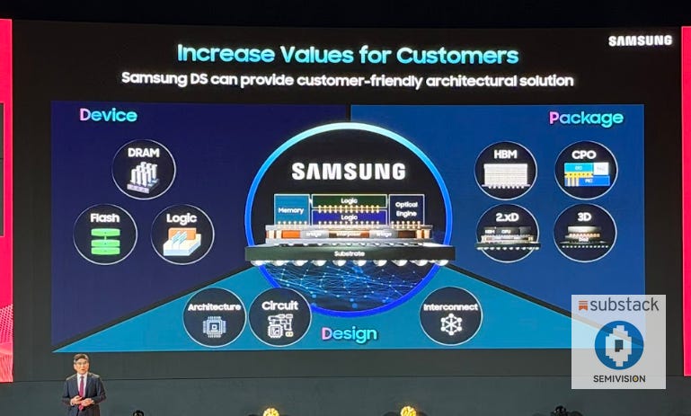
Samsung Electronics demonstrates a comprehensive and integrated strategy in the semiconductor sector through its Device Solutions (DS) division, positioning itself as a full-stack provider in the AI era. At the core is a customer-friendly architectural solution that bridges Device and Package technologies. On the device side, Samsung leverages its leadership in DRAM, NAND Flash, Logic, and advanced HBM (High Bandwidth Memory), with recent breakthroughs in HBM4 production and shipments driving significant revenue growth amid surging AI and data center demand.
In packaging, the company emphasizes innovations like CPO (Co-Packaged Optics) for high-speed, low-power optical interconnects, targeting commercialization around 2027, alongside 2.5D/3D advanced packaging solutions such as HBM stacking and custom architectures. This is complemented by strengths in foundry services, including 2nm process nodes and logic dies for customized HBM, enabling one-stop turnkey AI solutions that integrate memory, logic, optical engines, and interconnects.
By combining in-house expertise across architecture, circuit design, interconnect, and heterogeneous integration, Samsung aims to deliver optimized, high-value products that enhance performance, efficiency, and customization for customers. This holistic approach—focusing on profitability through premium AI-driven offerings like advanced DRAM, HBM, and next-gen foundry—seeks to strengthen long-term competitiveness against rivals while capitalizing on structural growth in AI infrastructure.

Samsung Electronics’ foundry capacity utilization rate exceeded 80% in the first quarter of this year, with some processes reaching as high as 90%, according to semiconductor industry sources on the 23rd. This marks a significant improvement from last year, when low customer orders kept utilization hovering around 50%.
The primary driver of this rebound is the Exynos 2600 processor, designed by Samsung’s System LSI division and manufactured in-house at the company’s Pyeongtaek foundry in Gyeonggi Province. The chip powers the base and Plus models of the new Galaxy S26, set to be unveiled this Thursday (Korea time), substantially boosting production demand.
In addition, NVIDIA’s robot chip series Thor and Tesla’s upcoming AI5 chip (design nearing completion) are slated for production by Samsung’s foundry division. Samsung is also poised to regain high-end chip orders from former major clients such as Qualcomm and AMD, as its advanced nodes—including the 2nm process used for Exynos 2600—show improved yields and performance.
This surge reflects growing confidence in Samsung Foundry’s capabilities, particularly in leading-edge processes, amid rising orders from global tech giants and strong internal demand from its mobile business.

2025年4月4日

2025年5月31日


PreviousNext
TopLatestDiscussions








See all