2026 NVIDIA Silicon Photonics 3D Stacking and DWDM Half-Rate Optical Link Technology
2026 NVIDIA Silicon Photonics 3D Stacking and DWDM Half-Rate Optical Link Technology
- Source: SemiVision
- Author: SEMIVISION
- Published: 2026-02-26T14:50:53+08:00
- URL: https://tspasemiconductor.substack.com/p/2026-nvidia-silicon-photonics-3d (1) 2026 NVIDIA Silicon Photonics 3D Stacking and DWDM Half-Rate Optical Link Technology


2026 NVIDIA Silicon Photonics 3D Stacking and DWDM Half-Rate Optical Link Technology
Original Article By SemiVision Reserach [Reading time: 30mins]

Feb 26, 2026
∙ Paid

NVIDIA Unveils a Breakthrough Silicon Photonics Paper at ISSCC 2026
SemiVision Provides an In-Depth Analysis of the Core Architecture
At ISSCC 2026 (International Solid-State Circuits Conference), NVIDIA presented a landmark paper titled:
“A 32Gb/s/λ 256Gb/s/Fiber Half-Rate Bandpass-Filtered Clock-Forwarding DWDM Optical Link in a 3D-Stacked 7nm EIC/65nm PIC Technology.”
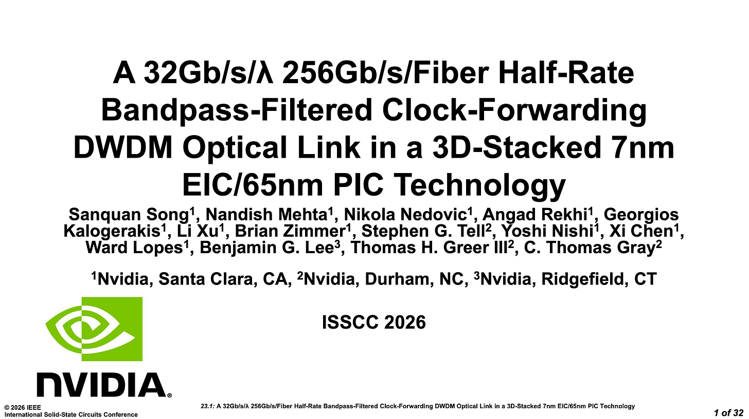
This publication formally reveals the technological blueprint behind NVIDIA’s next-generation AI infrastructure interconnect strategy.
Following an in-depth technical review, SemiVision concludes that this work is far more than a high-speed optical link design. Rather, it represents a strategic declaration of NVIDIA’s architectural direction for scalable AI interconnect systems.
Introduction: Data Interconnect Challenges in the AI Era
As the scale of artificial intelligence models grows exponentially, the rate of data exchange between computing resources increasingly becomes a bottleneck for overall system performance. Deep learning training requires hundreds—or even thousands—of GPUs or accelerators to work collaboratively, and these computing units must transfer massive volumes of weights, gradients, and activation data at very high speed.
Traditional electrical interconnects (such as PCIe or high-speed chip-to-chip links) encounter fundamental challenges when pushing beyond 100 Gb/s, including impedance mismatch, signal-integrity degradation, and sharply rising power consumption. To overcome these limitations, the industry has begun exploring optical interconnects based on silicon photonics, along with Dense Wavelength Division Multiplexing (DWDM) technologies.
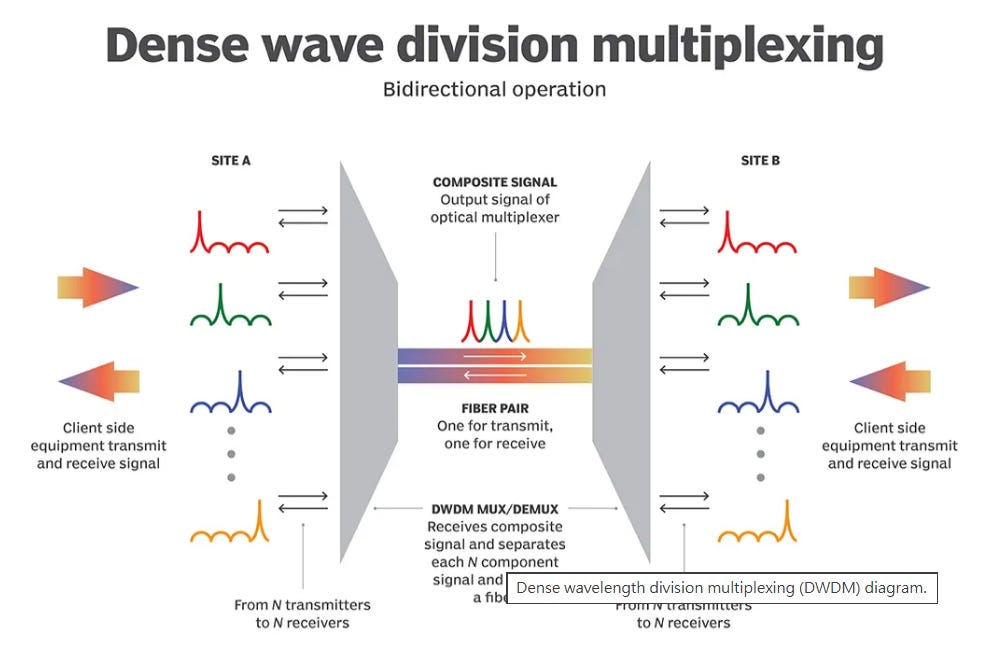
Source: TechTarget
By leveraging the ability of optical fibers to carry multiple wavelengths simultaneously, these approaches distribute data across multiple lower-speed wavelength channels rather than relying on a single ultra-high-speed lane. This strategy avoids the extremes of single-channel transmission while achieving a better balance among energy efficiency, scalability, and latency.
Challenges of Traditional High-Speed Electrical I/O
As 56 Gb/s, 112 Gb/s, and even 224 Gb/s channels emerge, the industry has broadly adopted higher-order Pulse Amplitude Modulation (PAM4, 4-level PAM) to increase bit rates. However, the increased number of symbol levels in PAM4 significantly raises signal-to-noise ratio (SNR) requirements, leading to reduced receiver sensitivity.
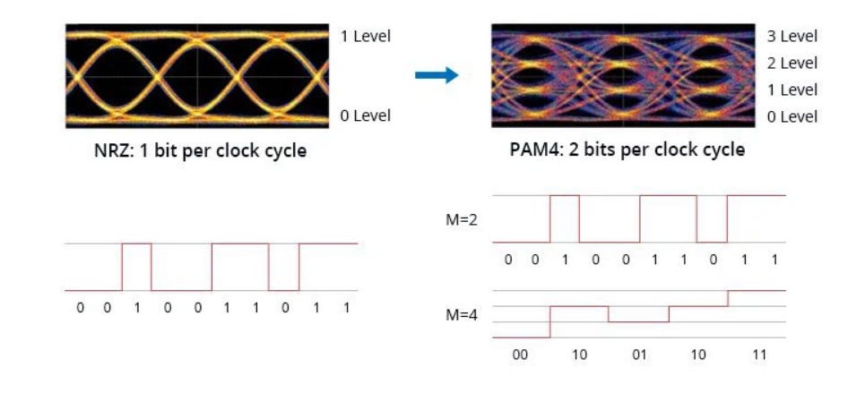
For example, achieving a 224 Gb/s channel requires a symbol rate of 112 Gbaud—effectively doubling the bandwidth. This places extremely stringent demands on a channel’s high-frequency response, crosstalk suppression, and equalization algorithms. In addition, even under optimal conditions, PAM4 exhibits a native bit error rate (BER) on the order of 1E-4 to 1E-6, making forward error correction (FEC) mandatory to reach the system-level requirement of 1E-12 or lower. FEC itself typically introduces more than 10 ns of additional latency.
These combined factors make ultra-high-speed electrical I/O increasingly difficult to scale in large-scale AI systems while simultaneously meeting the requirements for low latency and high energy efficiency.


2025年5月28日
For further reading on Co-Packaged Optics (CPO), please refer to the following articles.
In today’s era of explosive growth in AI training and inference workloads, data-center interconnects are under unprecedented pressure. As model parameter counts continue to scale and GPU clusters routinely expand to thousands of devices operating in parallel, interconnect bandwidth, density, and energy efficiency have become decisive bottlenecks for overall system performance.
However, the true technical challenge of DWDM links lies not merely in supporting multiple wavelengths, but in thechoice of clocking architecture. Traditional forwarded-clock (FC) schemes offer excellent jitter-tracking capability and are widely used in low-power chip-to-chip (C2C) links, but when directly applied to DWDM optical links, thermal noise from the transimpedance amplifier (TIA) introduces additional random jitter that can be amplified into multi-fold errors during data slicing. Embedded-clock (EC) architectures, on the other hand, are the mainstream approach for DWDM today, but they require clock-data recovery (CDR) circuits, increasing complexity. Moreover, the limited bandwidth of CDRs prevents effective suppression of out-of-band jitter originating from TX PLLs and power-supply noise. In short, both approaches offer advantages, yet each suffers from fundamental drawbacks.
The real breakthrough in NVIDIA’s ISSCC 2026 paper is the introduction of ahalf-rate bandpass-filtered forwarded-clock architecture, which successfully combines the strengths of both approaches while avoiding their weaknesses. Targeted at co-packaged optics (CPO) applications, the design employs nine wavelengths with 200 GHz spacing: eight channels carry 32 Gb/s NRZ data, while one channel is dedicated to a 16 GHz half-rate forwarded clock, achieving an aggregate throughput of 256 Gb/s per fiber. The key innovation is the application of a 1–2 GHz bandpass filter to the forwarded clock at the receiver. This bandwidth closely matches the TIA noise bandwidth, effectively filtering out uncorrelated random jitter introduced by the TIA. Meanwhile, data-correlated jitter—such as TX PLL jitter and supply-induced jitter—resides predominantly at low frequencies and is therefore fully tracked, keeping clock and data jitter aligned. This design dramatically reduces noise accumulation without requiring a CDR, achieving both ultra-low latency and high stability.
On the transmitter side, NVIDIA adopts a shared-clock, fully symmetric channel architecture. All nine TX channels share a single ring-oscillator-based TX PLL, distributing four half-rate phases to ensure multi-channel coherence at the source. Each TX channel integrates a phase interpolator to compensate for half-UI phase shifts and inter-channel skew, ensuring that sampling at the receiver is precisely aligned to the center of the data eye—without adding extra phase-generation circuitry on the RX side. The signal chain consists of a 16:1 serializer, S2D conversion, a TX driver, and a wideband level shifter. The level shifter uses a differential biasing scheme that allows the microring modulator to operate between high- and low-voltage nodes without being constrained by low cutoff frequencies, and it can tolerate leakage currents up to 300 μA, improving device compatibility and robustness. Notably, any TX channel can be configured via data mode to serve as the forwarded-clock channel, providing high flexibility in wavelength allocation.
The receiver design focuses on low noise and strong PVT (process, voltage, temperature) stability. The RX PLL is not used for clock distribution, but instead provides regulated bias references for the TIA and receiver circuitry, ensuring stable bandwidth across PVT variations. The TIA employs an inverter-based amplification topology combined with Cherry–Hooper cascades, and embeds an injection-locked oscillator (ILO). Together with the ILO in the clock-distribution path, this forms the core of the bandpass-filtering mechanism, strongly suppressing uncorrelated jitter while preserving low-frequency correlated jitter tracking. After the TIA, data and clock paths diverge: data is fed into a 1:16 deserializer, while the forwarded clock drives the ILO-based global clock-distribution network. To avoid the bandwidth limitations of a conventional 9:1 multiplexer, the design allows any RX microring to receive the forwarded clock and drive a distributed clock network. A dual-partitioned network reduces parasitic capacitance and power consumption, while improving laser fault tolerance and wavelength-assignment flexibility.
Thermal tuning is another critical component. Both TX and RX microrings incorporate mixed-signal closed-loop control. An 8-bit switched-capacitor ADC digitizes heater current, and a digital controller uses PI or peak-search algorithms to generate PDM signals that drive metal heaters, precisely locking wavelengths under low-power conditions. This tuning system ensures stable 200 GHz channel spacing across the full temperature range and under all PVT conditions.
From a process-integration perspective, the link uses a 3D hybrid-bonded stack of a 7 nm FinFET electronic IC (EIC) and a 65 nm SOI silicon-photonics PIC, with a 9 μm pad pitch. Electrical and optical channels are laid out in a one-to-one correspondence, placing photodiodes directly beneath their associated electrical channels. This dramatically shortens interconnect distances from TX drivers to microrings and from RX photodiodes to TIAs, reducing parasitic capacitance and inductance. The per-channel area is 80.94 × 80.94 μm², achieving an EIC shoreline density of 0.8 Tb/s/mm and an overall area density of 1.33 Tb/s/mm²—several times higher than contemporaneous NRZ DWDM designs.
Measured results show nine microring wavelengths clustered in the 1310 nm O-band with accurate 200 GHz spacing. Single-channel 32 Gb/s PRBS7 eye diagrams are clean, achieving an OMA sensitivity of −16.0 dBm at BER < 1E-11. With all channels transmitting PRBS31 simultaneously and forwarded-clock filtering enabled, the aggregated eye opening reaches 0.46 UI. Assuming a laser wall-plug efficiency of 10%, the overall energy efficiency is 2.78 pJ/b, broken down into 0.76 pJ/b for lasers, 0.76 pJ/b for microring heaters, and 1.26 pJ/b for circuitry and clock distribution.
Overall, this work represents not merely a single optical-link innovation, but a complete CPO architecture demonstration. Through half-rate bandpass-filtered clock forwarding, ILO-based jitter control, end-to-end thermal tuning, and 3D hybrid-bonded integration, NVIDIA achieves a balanced solution across high speed, low power, and high density. With 32 Gb/s per wavelength, 256 Gb/s per fiber, 2.78 pJ/b energy efficiency, and 1.33 Tb/s/mm² area efficiency—while maintaining a 0.46 UI eye opening at BER < 1E-11—the design demonstrates production-grade reliability. This architecture-level innovation provides a clear technical direction for next-generation AI data-center CPO optical engines, and signals that opto-electronic 3D co-design is poised to become the dominant paradigm for future high-end interconnects.
For further technical details, please refer to the sections below.
NVIDIA’s Strategy: Returning to 32 Gb/s NRZ with a Multi-Wavelength DWDM Architecture
In response to the challenges outlined above, NVIDIA proposed a solution that runs counter to prevailing industry trends in its ISSCC 2026 paper,“A 32 Gb/s/λ 256 Gb/s/Fiber Half-Rate Bandpass-Filtered Clock-Forwarding DWDM Optical Link in a 3D-Stacked 7 nm EIC/65 nm PIC Technology.”
Rather than pursuing ultra-high-speed 224 Gb/s PAM4 per channel, NVIDIA adopts 32 Gb/s non-return-to-zero (NRZ) modulation as the per-wavelength data rate. Using DWDM, eight data wavelengths plus one forwarded-clock wavelength are multiplexed within a single fiber, achieving an aggregate throughput of 256 Gb/s.
This “divide-and-conquer” approach keeps the per-channel data rate relatively low, making it easier to achieve low jitter and high reliability. Because it avoids the need for complex FEC or machine-learning-based equalizers, end-to-end link latency can be reduced to below 1 ns. Furthermore, NVIDIA employs 3D stacking to directly flip-chip bond a 7 nm electronic IC (EIC) onto a 65 nm silicon photonics IC (PIC). By leveraging hybrid bonding, the electrical-to-optical conversion distance is significantly shortened, improving power efficiency while reducing overall package footprint.
This article draws on publicly available literature and industry reports to provide an in-depth analysis of NVIDIA’s half-rate DWDM optical link. It first examines why 32 Gb/s NRZ offers advantages over 224 Gb/s PAM4, then introduces the use of DWDM and microring resonators on a silicon photonics platform. Next, it explains how bandpass-filtered clock forwarding reduces jitter, and finally analyzes the role of 3D stacked packaging and the implications for NVIDIA’s future roadmap.
Why Choose 32 Gb/s NRZ? — The Power and Jitter Dilemma of High-Speed Electrical I/O
Sensitivity Penalties Caused by Doubling PAM4 Data Rates
In conventional electrical channels, the bit rate carried on a single lane is determined by the symbol rate and the modulation scheme. NRZ modulation uses binary voltage levels, so the symbol rate equals the bit rate. PAM4 modulation, by contrast, employs four voltage levels, with each symbol carrying two bits, theoretically doubling the bit rate relative to the symbol rate.
However, the key advantage of PAM4 lies in increasing bit rate at agivensymbol rate—not in pushing the symbol rate higher. If the target is a 224 Gb/s port, the symbol rate must still reach 112 Gbaud, which places enormous demands on channel bandwidth and noise tolerance. According to analyses published inSignal Integrity Journal, insertion loss, crosstalk, and transmitter jitter increase sharply above 100 GHz. Transmitting PAM4 signals in this frequency range requires highly complex adaptive equalization and crosstalk cancellation, and these circuits become increasingly large and power-hungry at 224 Gb/s and beyond.
Sensitivity penalty is another major weakness of PAM4. Because PAM4 has four voltage levels, the voltage spacing between adjacent symbols is only one-third that of NRZ, making the signal far more susceptible to noise and jitter. Experimental data show that even under optimal conditions, the raw bit error rate (BER) of 224 Gb/s PAM4 systems typically falls in the range of 1E-4 to 1E-6. To meet network protocol requirements of 1E-12 or lower BER, strong forward error correction (FEC) is mandatory. However, FEC encoding and decoding introduce additional latency—often exceeding 10 ns—which is highly unfavorable for latency-sensitive AI training and inference workloads.
Simplicity and Reliability of NRZ Links
Compared with PAM4, NRZ modulation offers lower bandwidth efficiency at the same symbol rate, but it provides larger signal swing, higher jitter tolerance, and significantly simpler circuit implementation. For example, widely deployed 200G NRZ optical modules in the industry use eight 25 Gb/s NRZ lanes to achieve 200 Gb/s data rates within a QSFP-DD form factor, while consuming 2–3 W less power than comparable 4 × 50 Gb/s PAM4 modules.
Because NRZ modulation and demodulation are inherently simpler, clock jitter and overall circuit complexity can be substantially reduced. In latency-sensitive applications such as high-frequency trading or AI training, NRZ-based links can deliver end-to-end latencies below 1 ns.
For NVIDIA, setting the per-wavelength data rate at 32 Gb/s means each channel can rely on relatively mature, energy-efficient electro-optical modulators, while multiple wavelengths can be deployed on a silicon photonics platform using DWDM. This allows aggregate throughput to rival—or exceed—that of single-lane PAM4 systems operating at 200 Gb/s or higher. When combined with 3D stacked packaging that dramatically shortens the electrical-to-optical path, crosstalk and power consumption are further reduced, making the NRZ architecture an attractive solution for high-performance computing optical interconnects.
Dense Wavelength Division Multiplexing (DWDM): Stacking Channels Across Multiple Wavelengths
Principles and Advantages of WDM
Wavelength Division Multiplexing (WDM) enables a single optical fiber to simultaneously carry multiple optical signals at different wavelengths, with each wavelength corresponding to an independent data channel. According to white papers published by Smartoptics, these wavelengths can operate independently without mutual interference, as each channel uses a distinct “color” (i.e., frequency), allowing multiple data streams to be stacked within a single fiber. By deploying wavelength multiplexers/demultiplexers (Mux/Demux) at each end of the link, multiple independent data streams can be combined for transmission and then separated back into their respective wavelengths at the receiver.
As a result, WDM dramatically increases fiber utilization, reduces the number of fibers required, and scales overall system bandwidth. Modern DWDM systems can support up to 80 simultaneous wavelengths, enabling aggregate throughputs on the order of tens of terabits per second.
Implications for Silicon Photonics Platforms
On a silicon photonics platform, the essence of DWDM lies in the ability to precisely generate, modulate, and filter multiple closely spaced wavelengths. Silicon photonics materials—typically silicon-on-insulator (SOI)—feature a high refractive-index contrast, which allows the fabrication of waveguides and resonant cavities with extremely small bending radii.
A classic example is the microring resonator, which can selectively modulate specific wavelengths using ring waveguides with radii of only ~5 μm. With carefully engineered structures, microring resonators exhibit high quality factors (high-Q) and narrow spectral selectivity. They can simultaneously function as modulators, multiplexers, and filters, while offering strong miniaturization advantages that make them highly compatible with CMOS integration.
This capability allows silicon photonics to implement multi-wavelength DWDM functionality within a very small footprint, forming the foundation of NVIDIA’s 3D-stacked optical engine.

NVIDIA’s 8 + 1 Wavelength Architecture
NVIDIA’s DWDM link employs nine wavelengths spaced at approximately 200 GHz, distributed around the 1310 nm O-band (the near-zero dispersion window). Eight of these wavelengths carry 32 Gb/s NRZ data, while the remaining wavelength is used to forward a half-rate clock (discussed in detail later).
In this architecture, the modulators, photodetectors, and optical waveguides for each wavelength are all integrated on a 65 nm silicon photonics chip. Microring resonators are used to pack multiple wavelengths with tight spacing onto a single waveguide, and hybrid bonding is then applied to tightly couple the electronic drivers and amplifiers directly to the photonic devices.
This “8 + 1” structure strikes a balance between aggregate bandwidth and manageable per-channel data rates, while achieving excellent energy efficiency through well-distributed power consumption across wavelengths.
Microring Resonators (MRRs): The Critical Nodes of DWDM
Fundamental Operating Principles of Microring Resonators
A microring resonator is a ring-shaped waveguide structure. When the optical path length of the ring satisfies the resonance condition, light circulates within the ring, producing a narrowband filtering effect. The high refractive-index contrast between silicon and silicon dioxide allows microring resonators to achieve spectral selectivity on the order of tens of gigahertz—or even narrower—with extremely small ring radii of approximately 5 μm.
Key characteristics include:
Strong resonant field enhancement:Under resonance, the optical field inside the ring is significantly amplified, meaning that small electrical modulation or thermal tuning can induce substantial wavelength shifts.
Compact size and high quality factor:The small footprint allows multiple microrings to be placed only micrometers apart, saving die area and reducing process-induced stress. A high Q factor corresponds to a narrower filtering bandwidth.
Functional versatility:Microrings can operate as modulators (by changing the refractive index to modulate transmission), multiplexers (coupling multiple wavelengths into a single waveguide), or filters (rejecting non-target wavelengths), making them ideal building blocks for DWDM implementations.
Challenges and Mitigation Strategies
Microring resonators are highly sensitive to process variations and temperature fluctuations. Because the optical resonance condition depends on cavity length and refractive index, even nanometer-scale dimensional errors or small temperature drifts can shift the resonance frequency by tens of gigahertz, causing channel misalignment. To address these challenges, NVIDIA adopts several strategies:
Ring radius and channel spacing design:Microrings with radii of approximately 5 μm are selected, with each ring corresponding to one channel. Nine rings are evenly distributed across the 1310 nm band, with wavelength spacing of about 200 GHz. The small ring radius increases the free spectral range (FSR), keeping adjacent resonance peaks separated by ~200 GHz and reducing inter-channel crosstalk.
Thermal tuning and closed-loop control:Electrical heaters and control circuits are placed adjacent to each microring to thermally tune the resonance wavelength, ensuring precise alignment with the data or clock channels. Hybrid-bonded packaging further enables the integration of thermal couplers and temperature sensors between the silicon photonics die and the 7 nm electronic die, allowing real-time correction of thermal drift. Industry commentary suggests that, to reduce control-circuit power consumption, NVIDIA may employ injection-locked oscillators to generate reference signals for resonant thermal tuning, keeping control power in the hundreds-of-microwatts range.
Crosstalk modeling:The resonance response of microrings exhibits a so-called “long tail,” meaning that non-negligible transmission exists outside the main resonance peak. If poorly designed, these tails can introduce crosstalk between adjacent wavelengths. NVIDIA uses precise simulation and empirical characterization to model each ring’s tail response and adjust waveguide coupling coefficients and spacing, reducing inter-channel crosstalk to negligible levels. This careful engineering is a key reason the design can support nine wavelengths at 200 GHz spacing without significant interference.
Microrings as Modulators and Filters
In this DWDM architecture, microrings simultaneously function as modulators, filters, and multiplexers. On the modulation side, electro-optic modulators based on microring coupling are driven by 7 nm electronic amplifiers to achieve high-speed electrical-to-optical modulation. On the receive side, microring filters are used to select specific wavelengths and couple them into photodiodes.
Through precise biasing and current control within each channel, microring modulators can be linearized to improve modulation depth. Meanwhile, microring filters rely on fixed coupling coefficients and waveguide layouts to ensure balanced optical power distribution across all nine wavelengths.
Half-Rate Bandpass-Filtered Clock Forwarding: A New Architecture for Jitter Reduction
From Embedded Clocks to Forwarded Clocks
In high-speed serial links, common clocking approaches include embedded clocks and forwarded clocks. In an embedded-clock architecture, the clock signal is encoded within the data stream, and the receiver extracts it using a clock-and-data recovery (CDR) circuit. The advantage of this approach is that no dedicated clock channel is required; however, CDRs rely on wideband phase-locked loops (PLLs) to recover the clock and may amplify or convert uncorrelated noise in the signal into phase noise.
In optical DWDM systems, data carried on different wavelengths are inherently uncorrelated. An embedded-clock approach can therefore inject significant jitter across all channels, degrading eye opening.
An alternative is clock forwarding, in which the transmitter provides a dedicated clock channel and the receiver locks directly to the forwarded clock rather than recovering it from the data. NVIDIA’s approach reserves one of the nine wavelengths for a half-rate forwarded clock (Half-Rate Forwarded Clock), operating at 16 Gb/s. All receiver channels share this clock wavelength and generate local clocks using injection-locked oscillators (ILOs) in combination with bandpass filters (BPFs).
This architecture more effectively suppresses uncorrelated jitter because the BPF constrains the clock spectrum to a specific frequency band, allowing only correlated clock noise to pass through and thereby reducing phase noise at the receiver.
Operating Principles of the Bandpass Filter and ILO
In its ISSCC 2026 paper, NVIDIA introduces the concept of half-rate bandpass-filtered clock forwarding, with the following key elements:
Half-rate clock channel (16 Gb/s):Setting the clock rate to half the data rate lowers the clock frequency to 16 GHz. Half-rate bandpass filtering more effectively suppresses higher-frequency uncorrelated noise and also reduces the thermal tuning burden on microring resonators.
Bandpass filter (BPF):At the receiver front end, each channel includes a bandpass filter that removes spurious noise, allowing only clock-correlated phase noise to pass. As shown in the phase-noise comparison in Fig. 23.1.2 of the paper, architectures employing a BPF dramatically attenuate the power spectral density of uncorrelated noise, leaving primarily correlated noise and intrinsic system jitter. As a result, the overall phase-noise power spectral density (PN PSD) is significantly lower than that of embedded-clock or simple clock-forwarding architectures.
Injection-locked oscillator (ILO):After the BPF, the clock signal is fed into an ILO. An injection-locked oscillator is a locking mechanism that does not require a loop filter; it generates synchronous oscillation near the injected signal, with its phase noise governed by the injected clock. The ILO synchronizes the forwarded clock with a local oscillator and further filters high-frequency jitter. Compared with fully digital PLL-based approaches, ILOs consume less power, lock more quickly, and are well suited for massively parallel channels.
Half-rate sampling:Because the clock frequency is half the data rate, each receiver needs to sample only two decision points at the center of the data eye, rather than performing high-over-sampling. This reduces the power consumption and complexity of samplers, decision feedback circuits, and related logic. NVIDIA’s receiver architecture comprises a bandpass-filtered clock path, an ILO-based RX PLL, and timing-adjustment mechanisms for sampling phase alignment.
Impact on Jitter and Energy Efficiency
Bandpass-filtered clock forwarding significantly reduces phase noise in the data channels. When data and clock jitter within the same channel are highly correlated, the BPF allows these correlated components to propagate to the ILO while blocking noise unrelated to the data. The result is lower phase noise at the output clock, leading to increased eye opening.
Under 32 Gb/s NRZ operation, NVIDIA reports that the bit error rate (BER) can reach < 1E-11 at optimal link lengths, with receiver sampling unit-interval (UI) margin exceeding 0.64 UI—indicating ample jitter tolerance. Moreover, because traditional CDR elements such as charge pumps and loop filters are eliminated, the overall power consumption of the ILO + BPF architecture is substantially reduced, enabling an optical engine energy efficiency of just 2.78 pJ/b.
3D Stacked Packaging and Hybrid Bonding: Integrating Silicon Photonics with 7 nm Electronics
Principles of Hybrid Bonding
In conventional optical modules or board-level designs, electronic ICs and photonic ICs are typically connected using solder bumps or wire bonding. This requires relatively long metal interconnects between photonic devices and their driver circuits, increasing resistance and inductance and ultimately limiting achievable data rates. To approach ideal electro-optical coupling, NVIDIA—working with its foundry partners—adoptshybrid bondingtechnology, namely a 3D SoIC-X approach.

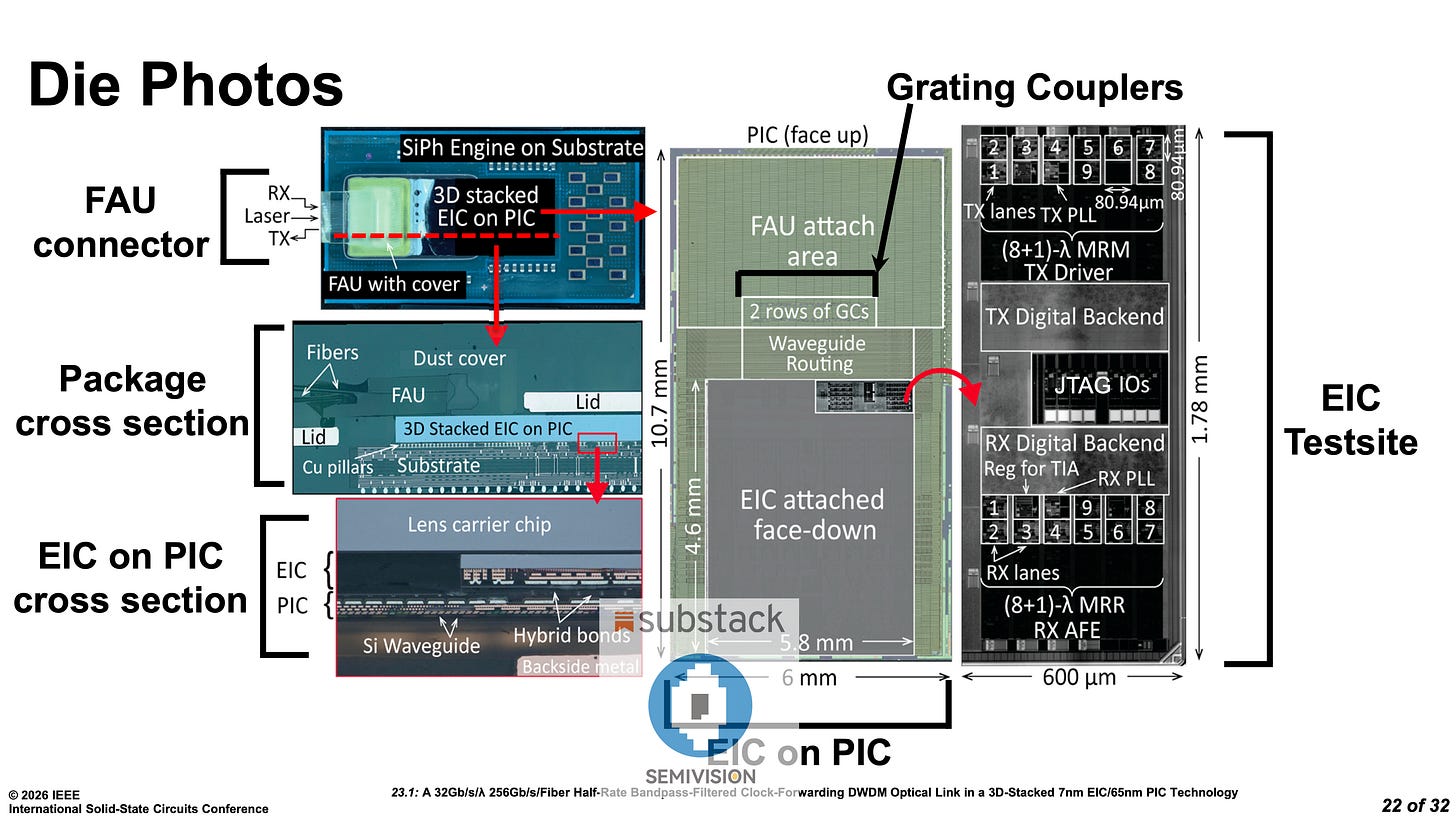
In this scheme, a 7 nm electronic IC is flip-chip bonded face-down directly onto a 65 nm silicon photonics IC, forming bumpless Cu–Cu interconnects with micrometer-scale alignment accuracy and interconnect pitches below 10 μm. This bonding method, often referred to as vertically integrated hybrid bonding, is a key member of TSMC’s advanced SoIC packaging family.
The hybrid bonding process involves first forming metal contact pads and oxide protection layers on both wafers. The wafers are then aligned face-to-face in a low-temperature environment so that the copper pads directly contact each other, followed by compression bonding. With controlled temperature and time, copper atoms diffuse across the interface to form a solid-state bond, resulting in an almost seamless metal-to-metal connection. By eliminating traditional solder bumps, hybrid bonding increases interconnect density, reduces resistance and inductance, and significantly lowers latency.

2025年6月12日
Stacking of 7 nm EIC and 65 nm PIC
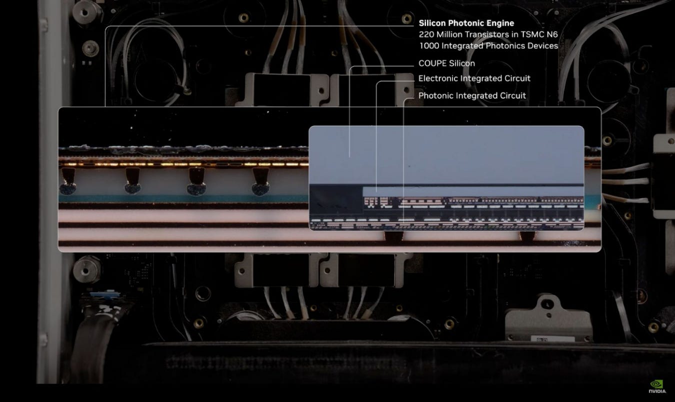
In NVIDIA’s optical engine design, the 7 nm electronic IC (EIC) primarily handles driver amplification, digital data-path logic, clock generation, and control functions, while the 65 nm silicon photonics IC (PIC) integrates optical waveguides, microring resonators, and photodetectors. After hybrid bonding, the photonics die faces upward, while the electronic die is flipped face-down on top of it. The resulting interconnect density can reach several thousand connections per square millimeter.
This architecture offers several advantages:
Shortened interconnect distances:Electro-optical conversion points are placed directly above the photonic devices, shrinking signal path lengths from hundreds of micrometers—or even millimeters—to just tens of micrometers, dramatically reducing RC delay and crosstalk.
Lower energy consumption:Reduced interconnect resistance and capacitance allow the same modulation depth to be achieved with lower drive voltage, or greater modulation depth at the same voltage, thereby reducing power consumption. According to IDTechEx, this stacking approach improves energy efficiency to as low as 2.78 pJ/b, which is critical for power optimization in AI clusters.
Higher bandwidth density:Thanks to vertical stacking, the entire optical engine occupies a footprint of only about 6 mm × 6 mm. Integrating nine microring resonators, waveguides, photodiodes, and their corresponding electronic drivers within this area yields a bandwidth density of approximately 1.33 Tb/s/mm²—far beyond what is achievable with traditional single-layer designs.
Simplified thermal management and testing:With electronic and photonic components in close proximity, thermal conduction paths are short, making it easier to use shared heat sinks or liquid-cooling solutions. Because the two dies are bonded at the wafer level and then diced, full wafer-level testing can be performed prior to packaging, improving manufacturing yield.
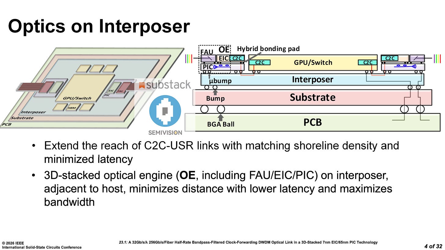
Optics on Interposer: Proximity Coupling to GPUs and Switches
NVIDIA not only stacks the optical engine within a module, but also places it near large chips—such as GPUs or switch ASICs—on a common interposer. According to NVIDIA’s demonstrations, the complete optical engine (OE), including the fiber attach unit (FAU), the 7 nm EIC, and the 65 nm PIC, is packaged at the edge of the interposer and connected to the GPU or switch chip via an ultra-short chip-to-chip (C2C) interface.
This“Optics on Interposer”architecture offers several benefits:
Shoreline density matching:Optical fiber coupling requires a certain physical pitch. Placing the optical engine at the interposer edge aligns naturally with the I/O shoreline density of the GPU, avoiding the need to crowd optical components into the chip core and improving scalability.
Minimized latency:The C2C distance between the optical engine and the GPU can be extremely short (potentially < 1 mm), allowing signals to travel from the GPU I/O die to the optical engine in just a few picoseconds—orders of magnitude lower than the several-nanosecond latency of traditional pluggable optical modules.
Improved serviceability and scalability:Analyses from APNIC suggest that NVIDIA’s open optical engine design allows multiple 1.6 Tb/s optical engines to be assembled into optical sub-assemblies (OSAs) that can be replaced individually, much like server fans. This greatly enhances maintenance flexibility. Because hybrid bonding reduces optical engine size and power, multiple engines can be distributed around a switch ASIC, enabling much higher aggregate system bandwidth.
Taken together, hybrid bonding and 3D stacking represent not only technological innovation, but also tangible manufacturing and operational advantages, paving the way for large-scale deployment of silicon photonics interconnects in future AI systems.
Implementation Architecture Analysis: 32 Gb/s NRZ × 8 + 1 Wavelengths = 256 Gb/s per Fiber
Data Channels and Clock Channel
NVIDIA’s implementation employs eight 32 Gb/s NRZ data channels and one 16 Gb/s half-rate clock channel. All nine wavelengths are arranged within the O-band spectrum with 200 GHz spacing. Each data channel is driven by a transmitter (TX) driver in the electronic IC (EIC), modulated via a microring resonator, combined into a shared waveguide, and finally coupled into the optical fiber. On the receiver (RX) side, microring filters and photodiodes separate the individual wavelengths, after which 7 nm RX circuits perform pre-amplification and decision-making.
The table below summarizes the main components of each channel:

Each channel corresponds to an individual microring, whose resonance wavelength is controlled via thermal tuning. Data-channel circuitry includes serial data generators, pre-drivers and modulators, as well as a digital backend (including JTAG I/O for testing). On the TX side, the clock channel uses a phase-locked loop (TX PLL) to generate the half-rate clock, which is then modulated by a microring and transmitted. On the RX side, the clock wavelength first passes through a bandpass filter, then an injection-locked oscillator generates a 32 Gb/s local clock that is distributed to all eight data channels.
TX Architecture: Multi-Ring Modulation and Voltage Control
The TX side includes a shared oscillator that distributes the clock to all TX channels. Each channel consists of cascaded pre-driver amplifiers and a microring modulator. Specifically:
Global oscillation and phase distribution:A ring oscillator generates a 16 GHz clock, which is delivered through a phase-distribution network to fractional-delay interpolators in the eight data channels. These interpolators adjust phase within the unit interval (UI) to ensure TX registers launch data at the optimal sampling point. Combined with injection-locking techniques, this compensates for clock skew caused by process and thermal variations.
Microring modulator driving:Each data channel employs a PN- or PIN-diode-based microring modulator. By applying reverse bias to alter the refractive index, the optical output intensity is modulated. Drive voltages typically range from 0.5 to 1.5 V and are often implemented with differential signaling to reduce single-ended ground noise. Because high-Q microrings are highly sensitive to voltage, the drivers must provide precise linearity.
Thermal tuning and bias control:Each microring is equipped with a heater and bias-control circuitry. Through digital control, resonance wavelengths are adjusted to compensate for process offsets and temperature drift. This control is implemented in the EIC digital backend and can execute calibration sequences to ensure all nine wavelengths remain aligned at 200 GHz spacing.
RX Architecture: Bandpass Filtering, Injection Locking, and Decision Logic
The RX architecture centers on bandpass filtering and injection-locked oscillation, with the following flow:
Optical reception and filtering:Nine microring filters couple the different wavelengths into their respective photodiodes (PDs). Because O-band signals exhibit low dispersion and nonlinearity, the PDs can provide high responsivity at 32 Gb/s, converting optical signals into electrical currents.
Transimpedance amplification (TIA):The photocurrent is converted into voltage by a transimpedance amplifier. To support half-rate clock forwarding, the clock-channel TIA is designed with wider bandwidth to pass the 16 GHz clock and its out-of-band noise. Data-channel TIAs can use narrower bandwidths to reduce noise.
Bandpass filtering and ILO:The clock-channel TIA output passes through a bandpass filter before entering an injection-locked oscillator. The ILO produces a 32 GHz local clock that synchronizes sampling across all channels. The BPF + ILO combination isolates signal-correlated phase noise while suppressing other noise components, significantly reducing jitter.
Energy Efficiency and Area Estimates
Based on publicly available information, this 32 Gb/s × 9-wavelength DWDM optical engine achieves an aggregate data rate of 256 Gb/s over a single fiber. Leveraging 3D stacking and half-rate clock forwarding, the overall link energy efficiency is approximately 2.51–2.59 pJ/bit, including the power consumption of the optical engine circuitry, clock generation, and thermal tuning.
The area efficiency reaches roughly 1.33 Tb/s/mm², representing a leading level in the industry. Compared with traditional co-packaged optics (CPO) approaches, NVIDIA’s optical engine delivers comparable or higher bandwidth within a smaller footprint, while offering superior energy efficiency relative to current 224 Gb/s PAM4 links.

2025年6月2日
Comparison with 224 Gb/s PAM4 Technology
Complexity and Power Consumption
In a 224 Gb/s PAM4 system, each lane operates at 112 Gbaud, with two bits per symbol. For an 8-lane module delivering around 1.8 Tb/s, extensive high-speed digital signal processing is required—including feed-forward equalization (FFE), decision-feedback equalization (DFE), and forward error correction (FEC)—to achieve acceptable BER over practical link distances. Implementing these functions demands dozens of high-speed SerDes, ADC/DAC blocks, and DSP cores, resulting in substantial power consumption.
By contrast, NVIDIA’s choice of 32 Gb/s NRZ across eight lanes eliminates the need for complex PAM4 slicers and high-order DSP. Replacing conventional CDRs with half-rate clock forwarding also removes many PLLs and digital calibration loops. As a result, at the same 256 Gb/s aggregate throughput, NVIDIA’s approach consumes roughly2–3× less powerthan traditional PAM4 solutions. At data-center scale, this energy-efficiency advantage translates into significant system-level power savings.
Latency and Jitter
224 Gb/s PAM4 links rely on FEC, introducing processing latency in excess of 10 ns. In addition, PAM4’s lower SNR requires more complex PLLs and CDRs with longer lock times. NVIDIA’s 32 Gb/s NRZ links, by contrast, achieve intrinsically lower BER and can reach below 1E-11 without FEC, keeping end-to-end link latency under 1 ns.
Half-rate clock forwarding combined with the BPF + ILO architecture further suppresses jitter and increases eye opening. For latency-sensitive AI workloads—particularly fully synchronous collective operations such as all-reduce—this ultra-low latency directly improves overall training throughput.
Scalability and Manufacturability
From a technology standpoint, PAM4 becomes increasingly difficult to extend to higher symbol rates. Achieving 224 Gb/s or even 448 Gb/s per lane may require PAM6 or PAM8 modulation, which suffers from even lower SNR tolerance and dramatically higher DSP complexity.
In contrast, NVIDIA’s DWDM architecture scales naturally by increasing the number of wavelengths or modestly raising per-channel data rates (e.g., to 40 Gb/s NRZ), while keeping each lane in a manageable speed regime. The highly repetitive design of microring resonators also simplifies process control and yield optimization. Hybrid-bonded packaging further facilitates testing and binning during manufacturing, improving overall module yield and scalability.

2025年5月27日
Packaging, Modularity, and System Integration
Modular Optical Engines: OSA and Field Replaceability
According to APNIC, NVIDIA’s Spectrum X and Quantum X switches adopt a modular optical-engine design, with each photonic engine delivering approximately 1.6 Tb/s of throughput. Three optical engines are combined into an optical sub-assembly (OSA), co-packaged with the switch ASIC on a shared interposer, and designed to be individually replaceable—much like server fans.
Reducing Laser Count and Sharing Optical Sources
A key advantage of NVIDIA’s CPO architecture is the substantial reduction in the number of required lasers. Traditional pluggable modules often dedicate a separate laser to each channel, or share a small number of lasers across channels, resulting in large numbers of laser modules and high overall power consumption.
APNIC’s analysis indicates that NVIDIA’s approach—sharing a small number of lasers across multiple wavelengths—reduces the total laser count by roughly4×compared with current competing solutions. This not only lowers cost but also simplifies thermal management of the laser sources. The laser modules can be placed outside the optical engine itself, for example in a fiber attach unit (FAU) or a shared optical-amplifier array, with wavelength multiplexers used to distribute optical power into the individual channels.
System-Level Integration
Reports fromTom’s HardwareandSiliconANGLEindicate that NVIDIA’s silicon photonics solution is closely aligned with TSMC’s COUPE (Co-Packaged Photonics) platform, with a roadmap extending toward 6.4 Tb/s and even 12.8 Tb/s optical engines.
First generation:Uses a 65 nm PIC stacked with a 7 nm EIC to achieve 1.6 Tb/s per optical engine.
Second generation:Likely to shrink the EIC process node to 5 nm or 3 nm while increasing the number of wavelengths.
Third generation:May adopt on-board lasers or integrated optical amplifiers, pushing total throughput to 12.8 Tb/s.
These optical engines are expected to be integrated directly into switches or GPU multi-chip modules (MCMs), replacing traditional pluggable optical modules and fundamentally reshaping data-center I/O architectures. When co-packaged with high-bandwidth memory (HBM), GPUs could interconnect directly with neighboring servers over ultra-low-latency optical links, forming optically accelerated clusters that deliver unprecedented compute density.

2025年5月2日
Market Impact and Future Outlook
CPO Market Forecast
According to IDTechEx, the Co-Packaged Optics (CPO) market is expected to grow rapidly over the next decade, surpassing USD 1.2 billion by 2035. Key drivers of this growth include the rising demand for compute performance and interconnect density in AI training and inference, the migration of switch silicon toward 51.2 Tb/s and beyond, and the data center industry’s urgent need to reduce power consumption.
As a leader in both GPU and networking technologies, NVIDIA’s 3D-stacked silicon photonics optical engine is likely to trigger a cascading industry effect, encouraging more cloud service providers and networking equipment vendors to invest in CPO development.
Technical Challenges
Despite its impressive results, NVIDIA’s approach still faces several technical challenges:
Thermal management:The performance of microring resonators and photodetectors is highly temperature-sensitive, requiring precise thermal control and robust heat dissipation. Hybrid bonding tightly couples the electronic and photonic dies, concentrating heat sources. Future higher-power optical engines may require liquid cooling or thermoelectric coupling to ensure stable operation.
Yield and process uniformity:Microring resonance frequencies are extremely sensitive to dimensional and refractive-index variations. Even with thermal tuning, process variation can lead to significant tuning power overhead. Ensuring that every microring remains within a controllable tuning range in high-volume manufacturing is a key challenge for large-scale DWDM silicon photonics.
System-level standards and interoperability:CPO currently lacks unified industry standards, with implementations differing in wavelength spacing, optical interfaces, and electrical interfaces. Broad deployment will require interoperable protocols and standardized test methodologies. If NVIDIA’s solution can align with Ethernet or widely adopted proprietary protocols, it would help accelerate standardization.
Future Outlook
As AI compute demand continues to surge, traditional electrical interconnects are unlikely to scale toward future link requirements exceeding 100 Tb/s. Silicon photonics combined with DWDM and 3D stacking offers an interconnect paradigm capable of parallelizing dozens of channels over a single fiber with ultra-low latency and minimal power consumption.
NVIDIA’s half-rate DWDM optical link demonstrates the feasibility of this path and lays the groundwork for subsequent breakthroughs. Looking ahead, GPUs and switches are expected to increasingly integrate optical engines—from board-level to chip-level integration, from passive coupling to on-board lasers and integrated amplifiers—ultimately enabling true “optical memory” and “optical interconnect” computing platforms.

2025年5月14日
SemiVision Viewpoint
NVIDIA’s ISSCC 2026 presentation of a 32 Gb/s/λ, 256 Gb/s-per-fiber half-rate DWDM optical link and its associated 3D stacking technology represents a clear departure from the industry’s push toward ever-higher single-lane PAM4 speeds of 224 Gb/s and beyond. By reducing per-channel data rates to 32 Gb/s and leveraging DWDM, microring resonators, and bandpass-filtered clock forwarding, NVIDIA achieves significant advantages in energy efficiency, latency, and scalability.
This work highlights the enormous potential of optical interconnects in the AI era. By combining multi-wavelength NRZ transmission, low-jitter clock forwarding, and 3D hybrid-bonded packaging on a silicon photonics platform, future data centers and supercomputers can overcome the fundamental limits of electrical interconnects and achieve unprecedented compute density and energy efficiency. As process nodes continue to scale, wavelength counts increase, and system-level standards mature, this class of optical interconnect architecture is well positioned to become a mainstream solution for next-generation AI systems. NVIDIA’s experimental results not only validate the technical feasibility of this approach, but also offer the industry a compelling strategic insight: rather than betting everything on extreme single-lane speeds, the future of interconnects lies in 3D stacking and massively parallel multi-wavelength architectures.

2025年4月8日


PreviousNext
TopLatestDiscussions








See all