Beyond Moore's Law: Rick Tsai's Bold Vision for AI's Next Semiconductor Revolution
Beyond Moore's Law: Rick Tsai's Bold Vision for AI's Next Semiconductor Revolution
- Source: SemiVision
- Author: SEMIVISION
- Published: 2026-02-24T09:14:19+08:00
- URL: https://tspasemiconductor.substack.com/p/beyond-moores-law-rick-tsais-bold (1) Beyond Moore's Law: Rick Tsai's Bold Vision for AI's Next Semiconductor Revolution


Beyond Moore's Law: Rick Tsai's Bold Vision for AI's Next Semiconductor Revolution
Original Article By SemiVision Research [Reading time: 12 mins]

Feb 24, 2026
∙ Paid
In San Francisco, amid the bustling halls of the International Solid-State Circuits Conference (ISSCC)—the premier global forum for breakthroughs in semiconductor design and systems-on-a-chip—MediaTek’s Vice Chairman and CEO, Rick Tsai, took the stage for a plenary keynote that resonated deeply with engineers, researchers, and industry leaders.
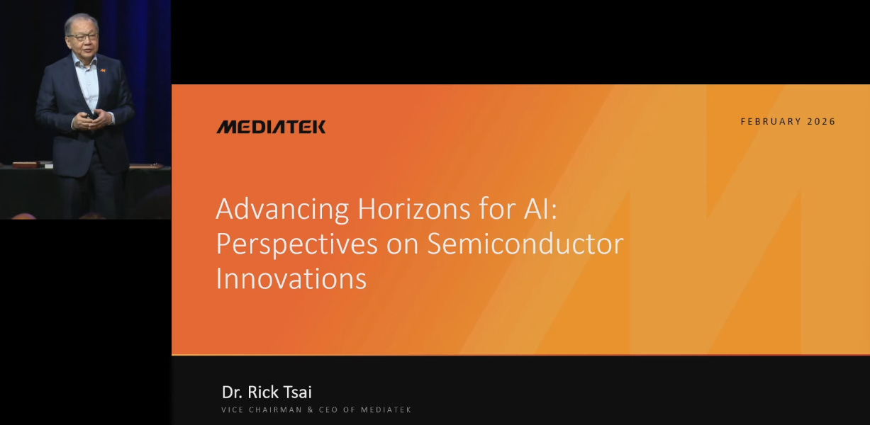
With over seven decades of history, ISSCC has been a beacon of rigor and international collaboration, fostering advancements that have shaped modern electronics. Tsai, a veteran in the semiconductor world with a career spanning leadership roles at TSMC and now steering MediaTek through the mobile and AI landscapes, expressed profound honor in addressing this community. His talk, titled “Advancing Horizons for AI: Perspectives on Semiconductor Innovations,” painted a vivid picture of our current moment: we are unequivocally in the AI era.

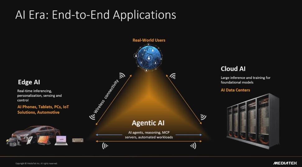
This era isn’t just a buzzword; it’s a transformative force akin to the dawn of the internet three decades ago, but with even greater implications for work, research, and society. Edge devices—smartphones, wearables, and IoT gadgets—are now integral to AI, serving as both direct interfaces and indirect enablers through data collection and processing. Yet, as Tsai emphasized, the real revolution is unfolding in the cloud, where massive models demand unprecedented computational power. Drawing from his experience at MediaTek, a company powering billions of devices worldwide, Tsai highlighted how AI’s impact will be “tremendous,” reshaping industries from healthcare to transportation. But this promise comes with challenges: escalating energy demands, supply chain strains, and the need for radical innovation in chip design.
As we delve into Tsai’s insights, it’s clear that the semiconductor industry stands at a crossroads. With global chip sales projected to hit nearly $1 trillion by 2026 or 2027—fueled by a 16% compound annual growth rate (CAGR) driven largely by AI—the stakes have never been higher.
Without AI, growth would languish below 10%, but hyperscalers like Google, Amazon, and Microsoft are pouring capital into data centers at a 25% CAGR, propelling the sector forward. This article explores Tsai’s vision, expanding on his key points with real-world context, technical explanations, and forward-looking analysis to provide a comprehensive view of the AI-driven semiconductor landscape.
2025年7月15日
The Shift to Cloud AI and Data Centers: From Edge to Exponential Demand
While edge devices have grown remarkably powerful—think of the neural processing units (NPUs) in modern smartphones enabling on-device AI for photo enhancement or voice recognition—Tsai argues they will never suffice alone. Model developers, from OpenAI to Google DeepMind, are relentlessly pursuing “better and bigger models” that require vast datasets and computational resources only available in the cloud. This shift marks a departure from the decentralized computing of the past, focusing instead on centralized data centers where AI thrives.
AI’s roots trace back decades, to the 1950s with early neural networks, but it was the abundance of computing power around 2012 that ignited machine learning’s boom. The availability of GPUs, pioneered by companies like Nvidia, allowed for parallel processing of massive data volumes, leading to breakthroughs in image recognition and natural language processing. By late 2022, generative AI—exemplified by ChatGPT—exploded onto the scene,
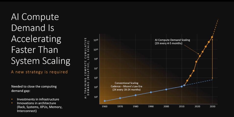
Creating a self-reinforcing cycle: more advanced models demand more compute, which in turn enables even larger models.
This exponential growth outpaces Moore’s Law, the longstanding principle that transistor counts double every 18-24 months, halving costs and boosting performance. Traditional scaling, which has delivered 2x improvements every 18 months, is no longer enough. As Tsai noted, AI’s hunger for compute is growing at rates that demand entirely new architectures. Consider the training of large language models (LLMs). Training GPT-3, released in 2020, consumed about 1.29 GWh of electricity—enough to power hundreds of homes for a year. Its successor, GPT-4, escalated to over 50 GWh, illustrating the voracious energy appetite of these systems.
Inference—the phase where models respond to queries—adds further demand; a single ChatGPT query uses roughly 2.9 watt-hours, nearly 10 times a standard Google search.This pivot to cloud AI necessitates hyperscale data centers, vast facilities housing thousands of servers optimized for parallel processing. Companies like Microsoft and Meta are investing billions, with data center construction booming globally. Yet, this centralization brings vulnerabilities: latency issues for real-time applications and dependency on robust connectivity.
The AI Economy: Fueling Semiconductor Growth to $1 Trillion

Tsai aptly dubs this the “AI economy,” where semiconductors are the bedrock. Hyperscalers are channeling massive capital expenditures into data centers, with projections showing a 25% CAGR over the coming years. This influx is catapulting the semiconductor industry toward $1 trillion in revenue by 2026 or 2027—a milestone that seemed distant just a few years ago. Absent AI, growth would hover below 10%, but with it, the sector enjoys a robust 16% CAGR.
This surge is evident in market data. In 2025, global semiconductor sales hit a record $791.7 billion, up 25.6% from the prior year, with AI chips comprising a significant portion. Deloitte estimates generative AI chips alone could generate $500 billion in 2026, nearly half of total chip revenues. Companies like Nvidia exemplify this: their fiscal 2025 revenue reached $130.5 billion, with projections soaring to $225 billion in 2026, driven by AI accelerators.
The economic ripple effects are profound. AI is democratizing innovation, enabling startups to leverage cloud resources without massive upfront investments.
In sectors like automotive, AI optimizes supply chains; in healthcare, it accelerates drug discovery. Yet, this growth isn’t uniform—memory and logic segments are exploding due to AI demands, while consumer electronics lag.Tsai’s perspective aligns with broader trends: the AI economy isn’t just about chips; it’s about ecosystems. Equipment sales for semiconductor manufacturing are forecast to hit $156 billion by 2027, up from $133 billion in 2025, with AI-related investments leading the charge. This boom underscores the need for strategic investments, as geopolitical tensions and supply chain disruptions loom.
The “Energy War”: Battling Power Constraints in the AI Boom

Amid this optimism, Tsai identifies a formidable obstacle: the “energy war.” Data center construction is accelerating, but power infrastructure lags, with energy needs doubling every six months or less. A large data center can guzzle 500 megawatts (MW) to 1 gigawatt (GW)—the latter matching San Francisco’s daily consumption.
Global data centers devoured 415 terawatt-hours (TWh) in 2024, about 1.5% of worldwide electricity, projected to double by 2030. In the U.S., consumption hit 183 TWh in 2024, expected to reach 426 TWh by 2030—4% of national use.
AI racks, drawing 30-100+ kW versus 7-10 kW for traditional ones, exacerbate this.Real-world examples abound: Northern Virginia’s data center hub experienced a 1,500 MW surplus from a voltage fluctuation, risking outages.
In Ireland, data centers consume as much power as the nation itself, straining grids. Water usage is another front; cooling requires millions of gallons daily, equivalent to small cities.

This “war” demands solutions: renewable integration, efficient cooling like liquid immersion, and policy incentives. Tsai warns that without addressing energy, AI’s potential could stall, echoing broader sustainability concerns.

2025年6月28日
System-Level Innovation: Rethinking the Rack for Heterogeneous Integration
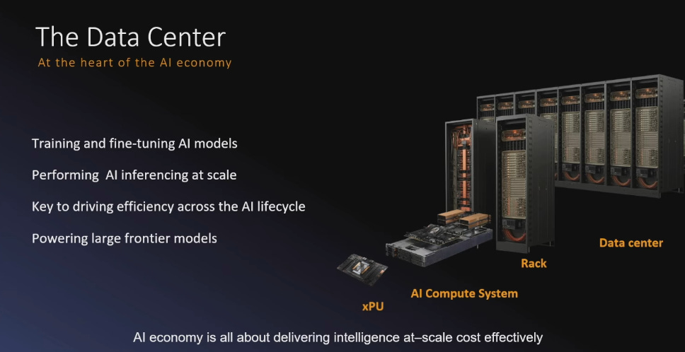
To combat these challenges, Tsai advocates shifting from chip-level to rack-level solutions. Racks—modular units housing servers—are now “ultimate heterogeneous integration platforms,” combining XPUs (AI accelerators like GPUs/TPUs), CPUs, and DPUs.
Key metrics: performance per watt (efficiency) and performance per total cost of ownership (TCO, including energy and maintenance). As XPUs scale to trillions of transistors, racks must optimize interplay between components.

This heterogeneous approach—mixing specialized dies—mirrors chiplets, where modular blocks reduce costs and boost yields. MediaTek’s Dimensity series exemplifies this in mobiles, but scaling to racks requires advanced interconnects and power management.
Industry-wide, this means collaboration: foundries like TSMC and Intel are ramping heterogeneous packages, with markets growing to $79 billion by 2030. Tsai’s call: move beyond siloed IPs to holistic systems.
Four Major Technical Challenges: Innovating for Sustainability
Sustaining AI growth hinges on four innovation pillars, as outlined by Rick Tsai in his ISSCC keynote. These challenges—compute, memory, interconnect, and advanced packaging—represent the critical bottlenecks that must be overcome to deliver the exponential performance, efficiency, and scale required for the AI era. Without breakthroughs in these areas, the industry’s trajectory toward ubiquitous, low-cost AI could falter amid escalating energy demands and diminishing returns from traditional scaling.
- Compute Innovations: Pushing the Boundaries of Transistor Density and Efficiency
The relentless pursuit of higher performance in AI accelerators demands continued advances in process nodes. Tsai highlighted the transition from today’s 4nm-class nodes to 1.4nm (often denoted as A14 or similar in roadmaps), which promises a roughly 2.5x increase in transistor density. This density boost enables larger, more capable XPUs with hundreds of billions—or even trillions—of transistors, essential for handling increasingly complex generative AI models.
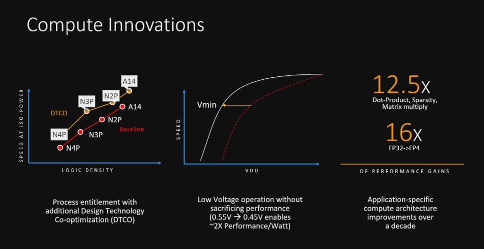
However, raw density alone isn’t enough; power efficiency is paramount in an era where data centers face an “energy war.” Lowering supply voltage is a key lever to reduce dynamic power consumption while maintaining or improving performance. Foundries like TSMC are targeting mass production of 1.4nm nodes around 2027–2028, with risk production potentially starting as early as late 2026. Competitors such as Samsung and Intel are pursuing similar timelines, incorporating gate-all-around (GAA) transistors and high-NA EUV lithography to achieve up to 15–30% better performance-per-watt compared to prior generations.
Beyond hardware scaling, Tsai stressed the need for closer collaboration between mathematicians and engineers to design application-specific architectures. Examples include specialized tensor cores in GPUs, optimized for matrix multiplications central to neural networks, or custom silicon tailored for inference-heavy workloads. These domain-specific designs can yield outsized gains by avoiding the inefficiencies of general-purpose computing.Market projections underscore the momentum: leading-edge logic (foundry and advanced node) equipment spending is forecasted to reach approximately $75 billion by 2027, driven by AI accelerators, high-performance computing, and premium mobile processors. This investment reflects the industry’s bet that compute innovations will remain a cornerstone of AI progress through the end of the decade.
- Memory: The Rising Cost Center and Bandwidth Bottleneck
Memory has evolved from a supporting player to a dominant factor in AI system design. Tsai noted that memory now accounts for about 50% of the bill of materials (BOM) cost in sophisticated XPUs (AI accelerators). This shift stems from the insatiable demand for high-bandwidth, low-latency access in training and inference.
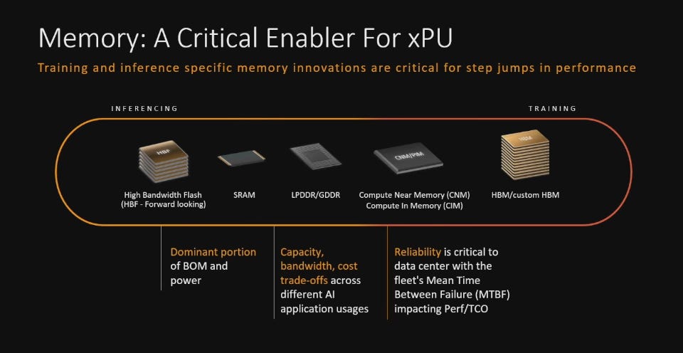
A prime example is Nvidia’s Blackwell architecture, which integrates up to 192GB of HBM3e memory per GPU—more than double the capacity of prior generations like the H100 (80GB HBM3) or H200 (141GB HBM3e). This massive on-package memory enables bandwidths reaching 8 TB/s, critical for feeding data to thousands of cores without stalling computations. Yet, the surge in HBM adoption has created severe shortages, with prices surging dramatically—some reports indicate 50%+ hikes in quarters amid sold-out supply through 2026.
The industry is in the midst of an HBM-led “supercycle”, fueled by AI prioritization. HBM demand is projected to grow explosively, with the market potentially reaching tens of billions in value by 2026–2028. Traditional DRAM and NAND face ripple effects, as manufacturers like SK Hynix, Samsung, and Micron redirect capacity toward higher-margin HBM, leading to broader memory price inflation and constraints on consumer segments.

2月12日
To address these challenges, Tsai called for innovations in higher bandwidth, improved reliability, and novel architectures like compute-in-memory (CIM). CIM integrates computation directly within the memory array—performing operations such as vector-matrix multiplications in-place—drastically reducing data movement between memory and processors.
This approach mitigates the “memory wall” by slashing energy costs and latency, particularly for AI workloads dominated by repetitive data accesses. Emerging CIM implementations leverage resistive memories (e.g., ReRAM or MRAM) or analog techniques, promising significant efficiency gains, though challenges like device variation, precision, and scalability persist.
- Interconnect: Eliminating the “Tax” on Performance
Interconnects—whether die-to-die within a package or rack-to-rack across a data center—impose a heavy “tax” in the form of latency, energy consumption, and bandwidth limitations. As AI clusters scale to thousands of accelerators, traditional electrical links (e.g., copper-based SerDes) struggle to keep pace, especially over longer distances.
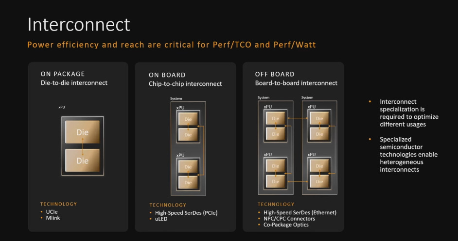
Tsai pointed to co-packaged optics (CPO) as a transformative solution. CPO integrates photonic components directly with the switch ASIC or accelerator package, converting electrical signals to optical ones at the chip level. This slashes power use (up to 3.5x reductions in some implementations), boosts bandwidth density, and extends reach while minimizing heat and signal degradation.

2025年6月17日
Industry progress is accelerating: Nvidia has introduced CPO-based platforms like Quantum-X Photonics and Spectrum-X Photonics, with commercial availability starting in 2025–2026 for InfiniBand and Ethernet switches. Broadcom, Marvell, and others are advancing 1.6T to 6.4T optical engines, targeting hyperscale AI networks. Market forecasts project the CPO sector growing at 30–37% CAGR, potentially exceeding $20 billion by the mid-2030s, driven by AI scale-up and scale-out demands.

2025年6月4日
By replacing copper bottlenecks with photonics, CPO enables larger, more efficient AI “factories,” supporting the massive interconnect bandwidth needed for trillion-parameter models and distributed training.
- Advanced Packaging: Enabling Larger, More Integrated Systems
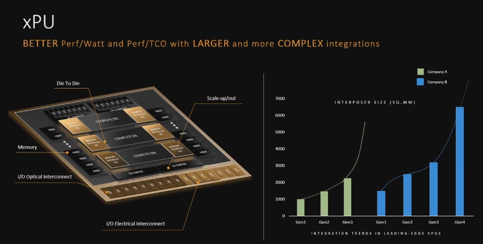
As chips grow in complexity, traditional packaging limits integration. Tsai envisioned packages expanding to iPad Pro-like sizes—up to 20,000 mm²—by 2030, necessitating 3D stacking to achieve the required density without prohibitive area costs.
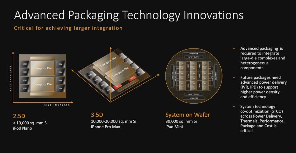
Advanced packaging technologies like 2.5D/3D-IC (e.g., TSMC’s CoWoS, Intel’s EMIB, or hybrid bonding) allow heterogeneous integration of logic, memory (HBM stacks), and accelerators into a single module. This reduces interconnect lengths, boosts performance, and improves power delivery.
Key enablers include breakthroughs in thermal management—such as liquid cooling, immersion, or advanced TIMs (thermal interface materials)—and power delivery networks to handle kilowatt-scale loads without hotspots. Multidisciplinary collaboration is essential, drawing in mechanical engineers, materials scientists, and thermal experts.

2月10日
The advanced packaging market is booming, with projections from Yole Group indicating growth to around $79–83 billion by 2030 (CAGR ~9–10% from 2024 levels), fueled by AI and HPC. The 3D-IC subset alone supports dense stacking critical for next-gen AI chips.
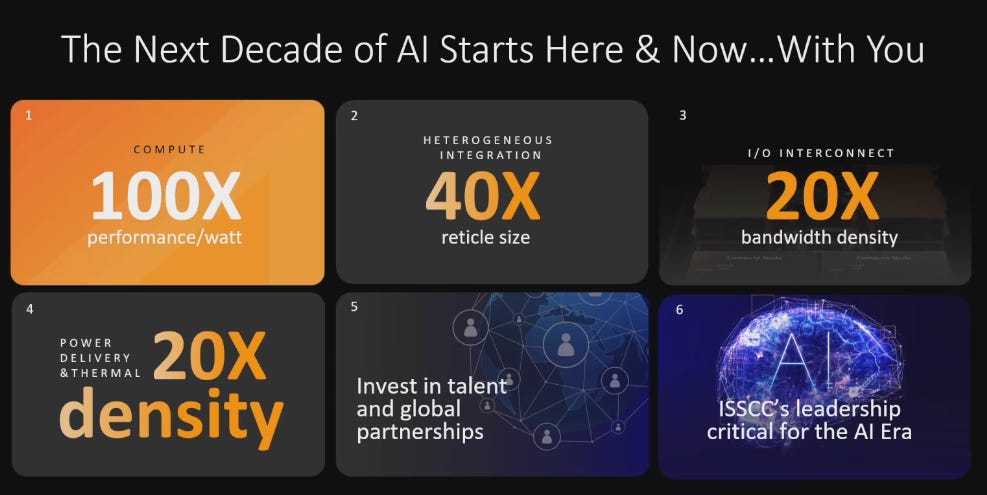
These four pillars are interdependent: compute gains demand denser memory and interconnects, which in turn rely on advanced packaging. Overcoming them requires ecosystem-wide innovation—from foundries and designers to materials suppliers and hyperscalers. As Tsai challenged the community, achieving 100x performance-per-watt improvements by the mid-2030s will demand nothing less than a paradigm shift, paving the way for truly ubiquitous AI accessible to all at minimal cost. The path is arduous, but the rewards—sustainable, scalable intelligence—could redefine society.

1月26日
A Call to Action: 100x Efficiency by 2030 and Ubiquitous AI
The roadmap to 2030 is clear—node shrinks, packaging advances—but beyond demands audacious goals. Tsai challenges the community: achieve 100x performance-per-watt improvement in 10 years, outstripping Moore’s Law.
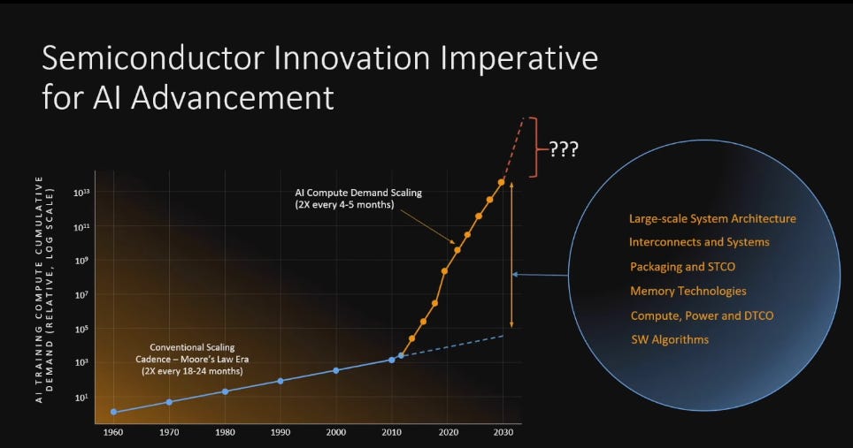
This vision: ubiquitous AI, accessible at low or no cost, democratizing benefits from personalized education to global problem-solving. Yet, it hinges on overcoming formidable energy and innovation barriers.
In conclusion, Rick Tsai’s keynote serves as a powerful rallying cry for the semiconductor world. As AI reshapes society at an unprecedented pace, the industry must innovate boldly and collaboratively to ensure sustainable, scalable growth. Recent analyses, including McKinsey’s projections, point to the semiconductor market potentially reaching $1.6 trillion by 2030—a figure driven largely by AI’s insatiable demand for leading-edge logic, high-bandwidth memory, and system-level advancements.The opportunities are immense—but so are the responsibilities, particularly around energy.
From SemiVision’s perspective, energy will be the defining big issue of the next decade. Tsai’s “energy war” warning is already materializing: data center power demands are exploding, with global electricity consumption for data centers projected to roughly double to around 945 TWh by 2030 (per IEA estimates), and AI-accelerated servers growing at 30% annually. In the US alone, AI data centers could push demand toward 50–123 GW or more by 2030–2035, straining grids, driving up costs, and risking regional bottlenecks or blackouts if infrastructure can’t keep pace.
Without aggressive breakthroughs in performance per watt (Tsai’s 100x challenge), advanced power delivery, thermal solutions, renewables integration, and even rethinking data center locations, the AI supercycle could hit a hard wall—slowing progress, inflating prices, or forcing compromises on accessibility. The path to truly ubiquitous, low-cost AI isn’t just about more transistors or bigger models; it’s about mastering energy efficiency at every layer. The AI era is here; now, we must build its sustainable foundation—or risk watching the promise stall under its own power-hungry weight.

2025年5月21日


PreviousNext
TopLatestDiscussions








See all