TSMC in 2026: Full Power On, Racing to Max Out Capacity
TSMC in 2026: Full Power On, Racing to Max Out Capacity
- Source: SemiVision
- Author: SEMIVISION
- Published: 2026-02-23T11:51:41+08:00
- URL: https://tspasemiconductor.substack.com/p/tsmc-in-2026-full-power-on-racing (1) TSMC in 2026: Full Power On, Racing to Max Out Capacity


TSMC in 2026: Full Power On, Racing to Max Out Capacity
Original Article By SemiVision Research [Reading time: 10 mins]

Feb 23, 2026
∙ Paid
TSMC’s Rapid Fab Expansion Across Taiwan: Racing to Meet Soaring AI Chip Demand
As artificial intelligence continues to reshape industries worldwide, TSMC is in full acceleration mode, aggressively building and upgrading fabrication facilities across Taiwan to bridge the widening gap between explosive customer demand—particularly from AI leaders like NVIDIA—and available production capacity.
In early 2026, TSMC’s construction sites are buzzing with activity from north-central to southern Taiwan, focusing on both leading-edge logic processes (such as A14, N2, and A16) and critical advanced packaging technologies like CoWoS (Chip on Wafer on Substrate). These expansions are essential for producing the complex, high-performance multi-die AI accelerators that integrate massive logic chips with high-bandwidth memory (HBM), powering trillion-parameter models and next-generation data centers.
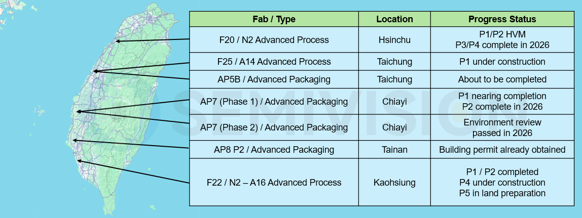
Key highlights from TSMC’s ongoing Taiwan build-out include:
In northern Taiwan’s Hsinchu Baoshan area, TSMC’s F20 fab has already entered mass production phase. P1 is ramping up, with monthly capacity expected to reach 10,000 wafers by the end of the year. P2 has been completed and commissioned, while P3 and P4 are under intense construction and are scheduled for completion in 2026.
In Taichung (Central Taiwan Science Park), F25 (A14 advanced process) is actively under construction for P1, while AP5B (advanced packaging) is nearing completion and poised to come online soon, adding vital CoWoS capacity to support current AI workloads.
In Chiayi (Southern Taiwan Science Park), AP7 Phase 1 is nearing completion with P1 close to wrap-up and P2 about to be finished, while Phase 2 has cleared its environmental review in 2026. This site is rapidly evolving into a major hub for next-gen packaging innovations like WMCM, SoIC, and CoPoS, with production ramps targeted for 2026–2027 to quadruple overall CoWoS output.
In Tainan (Southern Taiwan Science Park), AP8 P2 has already secured its building permit, positioning it for swift progression and contributing to the region’s growing role in advanced packaging.
In Kaohsiung (Nanzi Technology Park), F22 (N2–A16 advanced process) shows strong momentum: P1 and P2 are already completed, P4 is under construction, and P5 is in the land preparation and piling phase—setting the stage for future high-volume output of sub-2nm nodes.
This multi-site, multi-phase push is no coincidence. Driven by unrelenting orders from hyperscalers and AI chip giants, TSMC aims to dramatically scale CoWoS monthly capacity toward 120,000–140,000+ wafers by late 2026, a multi-fold increase from recent levels. Even as leading-edge logic fabs in Hsinchu and Kaohsiung ramp 2nm and beyond, advanced packaging has emerged as the primary bottleneck—making these Taiwan expansions the linchpin for delivering the hardware behind the AI revolution.
By spreading investments across Taichung, Chiayi, Tainan, and Kaohsiung science parks, TSMC not only boosts throughput but also enhances supply-chain resilience and geographic diversification within Taiwan. The result: faster fulfillment of massive backlogs, shorter lead times for customers, and sustained momentum in the global semiconductor race. In an era where AI compute demand shows no signs of slowing, TSMC’s rapid factory-building campaign underscores its commitment to staying ahead—ensuring the world gets the chips it needs, when it needs them most.

2025年4月1日
In the heart of Taiwan’s Chiayi Science Park, a tale of ancient history colliding with cutting-edge technology unfolded in 2024. As construction crews broke ground for Taiwan Semiconductor Manufacturing Company’s (TSMC) ambitious P1 advanced packaging plant in May, they unearthed artifacts from a bygone era—fragments of cord-marked pottery, human burials, and other relics hinting at prehistoric settlements.
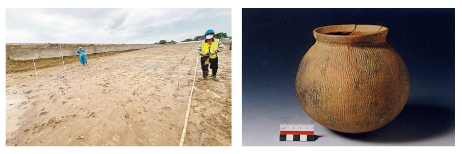
Cord-Marked Pottery (繩紋陶) — as the name suggests — refers to pottery sherds decorated with cord impressions. These patterns were likely created in one of two main ways: either by pressing a cord-wrapped paddle (陶拍) against the clay surface, or by rolling a cord-wrapped stick or baton over the vessel while it was still soft.
This discovery, under Taiwan’s Cultural Heritage Preservation Act, triggered a partial halt in construction to allow for archaeological salvage operations. What followed was a months-long excavation that delayed the project by half a year, yet TSMC’s resolve to meet its 2027 production targets remained unshaken. Even during the Lunar New Year holidays in early 2026, the site blazed with activity—lights piercing the night sky on the first evening of the festivities, transforming the area into a beacon of industrial determination visible from the nearby high-speed rail station.
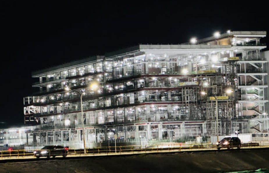
This scene encapsulates TSMC’s broader narrative in the AI era: a company navigating unexpected setbacks while racing to expand capacity amid exploding global demand for advanced semiconductors. As the world’s leading contract chipmaker, TSMC powers everything from smartphones to supercomputers, but its role in artificial intelligence (AI) has catapulted it to unprecedented heights. With clients like NVIDIA pushing the boundaries of AI hardware, TSMC’s investments in advanced logic processes and packaging technologies are not just business decisions—they’re pivotal to the future of computing. This article delves into the Chiayi project’s challenges, TSMC’s strategic expansions, safety commitments, financial triumphs, and the symbiotic relationship with AI giants, painting a picture of a semiconductor powerhouse adapting to an ever-accelerating tech landscape.
The Archaeological Interlude: Unearthing the Past Amid Future Builds
The story began in late May 2024 when routine site preparation for the P1 plant—part of TSMC’s Advanced Backend Fab 7 (AP7) complex—revealed suspected archaeological ruins.

Primarily red pottery featuring finely impressed cord-marking, with a refined and delicate fabric; vessel forms include jars (罐), bowls (缽), stemmed bowls/dou (豆), and other types.
Cord-marked pottery, characteristic of Neolithic cultures in Taiwan, along with ceramic shards and human remains, prompted immediate intervention by local authorities. Under the Cultural Heritage Preservation Act, TSMC was required to suspend portions of the work to facilitate a rescue excavation. This wasn’t just a minor hiccup; it represented a clash between Taiwan’s rich cultural heritage and its modern economic engine—the semiconductor industry, which accounts for over 15% of the island’s GDP.
Archaeologists descended on the site, conducting meticulous digs over several months. By November 2024, the salvage was deemed complete, allowing construction to resume.
The delay, however, pushed back timelines significantly. Originally slated for rapid progress, P1’s setback contrasted with the smoother advancement of its sibling, P2, which had already begun equipment installation in 2025 and is on track for mass production in 2026.
To compensate, TSMC ramped up efforts, turning the Lunar New Year—a time traditionally reserved for family and rest—into a non-stop construction marathon. Workers toiled through the nights, with the site’s illuminated cranes and machinery becoming a symbolic landmark in the Chiayi High-Speed Rail Station district.
This incident highlights broader trends in semiconductor manufacturing. As fabs expand into new areas, environmental and cultural considerations increasingly intersect with industrial ambitions. In Taiwan, where land is scarce and history runs deep, such discoveries are not uncommon. TSMC’s handling of the situation—cooperating with authorities and even sparking public interest in archaeology—demonstrates a maturing approach to corporate responsibility. Yet, the six-month delay underscores the fragility of supply chains in an industry where time is money. For context, the global semiconductor market is projected to reach $1 trillion by 2030, driven largely by AI, with packaging technologies like CoWoS (Chip on Wafer on Substrate) becoming bottlenecks.
TSMC’s ability to recover from such interruptions is crucial, as any prolonged hiccup could ripple through the AI ecosystem, affecting everything from data centers to consumer electronics.
2月2日
Media Spotlight: Unveiling Chiayi’s Advanced Packaging Hub
On January 22, 2026, TSMC opened the doors of its Chiayi facility to the media for the first time, hosting a guided tour that showcased the AP7 complex’s potential.
The event was more than a publicity stunt; it was a declaration of intent. TSMC announced plans to further expand investments in the site, positioning it as potentially the company’s largest advanced packaging hub. With AI chips requiring intricate integration of logic dies and high-bandwidth memory (HBM), facilities like AP7 are vital for technologies such as CoWoS, which enable the dense, high-performance packaging needed for NVIDIA’s GPUs.
The tour emphasized the site’s role in TSMC’s southern Taiwan strategy, part of the “S-type Technology Corridor” that includes Kaohsiung and Tainan. P2, already equipped and ready for production this year, will focus on Wafer-Level Multi-Chip Module (WMCM) initially, supporting demands from clients like Apple.
This expansion aligns with industry forecasts: advanced packaging revenues are expected to grow at a 24% CAGR from 2025-2027, fueled by AI and high-performance computing (HPC).
Beyond the hardware, the event highlighted TSMC’s commitment to safety. In November 2025, the company released its “Construction Site Safety Declaration,” reaffirming safety as the top priority in all building projects.
This includes establishing high-standard separation between construction and supervision, enlisting international third-party experts for on-site reviews, and optimizing mechanisms across safety awareness, behavior, and environment. Such measures are timely, given past concerns at TSMC sites, including those in Arizona.
In an industry where complex fabs involve hazardous materials and high-risk operations, these protocols not only mitigate risks but also enhance TSMC’s reputation as a responsible employer.

2025年4月19日
Safety First: Building a Culture of Protection
TSMC’s safety emphasis extends beyond declarations. The company’s Occupational Safety and Health Policy, applicable to all subsidiaries, focuses on creating a zero-accident environment through rigorous risk management and supplier collaboration.
In 2024, TSMC ensured 100% of high-risk contractors were ISO 45001 certified, and it introduced on-site ambulances and emergency technicians at new sites.
These efforts are part of a broader trend in semiconductors, where fab complexity has heightened safety demands. For instance, handling extreme ultraviolet (EUV) lithography and advanced materials requires protocols that prevent chemical exposures and structural failures.

At TSMC construction and operation sites, Toolbox Meetings are conducted regularly before work begins.
At Chiayi, this translates to enhanced training for workers, including mandatory ESH (Environmental, Safety, and Health) courses for contractors.
The company’s 2024 initiatives, such as partnering with hospitals for health monitoring and promoting mental health during World Mental Health Month, reflect a holistic approach. As TSMC expands globally—with fabs in the US, Japan, and Europe—standardizing these practices ensures consistency while adapting to local regulations. In the AI-driven boom, where speed is paramount, these safeguards prevent costly disruptions, allowing projects like P1 to proceed safely amid round-the-clock efforts.
Capacity Ramp-Up: Meeting the AI Surge
TSMC’s investments in Taiwan underscore its strategy to dominate advanced nodes. The company continues R&D in leading-edge logic and packaging, with Chiayi’s AP7 joining other sites like Zhongke’s AP5B and Kaohsiung’s F22 P3.
P2’s 2026 production and P1’s 2027 target aim to satisfy the “explosive demand” for AI chips. By late 2026, TSMC plans to quadruple CoWoS capacity to 130,000 wafers monthly, making Chiayi the world’s largest packaging hub.
This expansion is intertwined with NVIDIA’s roadmap. As AI models scale to trillions of parameters, chips like Blackwell and upcoming Rubin require HBM4 and CoWoS-L.
NVIDIA has booked over 50% of TSMC’s CoWoS lines for years ahead, leaving competitors scrambling.
TSMC’s fabs operate non-stop, even during holidays, to meet this demand. Looking ahead, processes like A16 and N2P, set for H2 2026 production, promise lower power consumption and higher density for AI accelerators.
NVIDIA’s Spotlight: Earnings and Innovations
NVIDIA’s trajectory amplifies TSMC’s urgency. The AI leader’s Q4 2025 earnings, due February 25, 2026 (local time), are expected to show robust growth from Blackwell demand.

Rubin, expanding to six chip variants with HBM4 and CoWoS-L, will drive 2026 growth. TheGTC 2026 conference, March 16-19 in San Jose, promises revelations—CEO Jensen Huang teases a “world-surprising” chip, possibly the A16-fabricated “Feynman” with backside power delivery.

This innovation could leapfrog rivals, leveraging TSMC’s scale. Such announcements validate AI’s fundamentals, with spending on infrastructure soaring. TSMC’s layouts—AP7 P1/AP5B completions in 2026, AP8 P2 permits secured—position it as the backbone of this ecosystem.
Financial Fortitude: Record Revenues and Rewards
TSMC’s January 2026 revenue hit NT$401.26 billion, surging 36.8% year-over-year and 19.8% month-over-month, bucking seasonal Lunar New Year dips.
Q1 guidance: NT$1.11 trillion midpoint, up 35.6-40.3% YoY. This strength stems from AI-driven orders. Employee rewards reflect this prosperity. This week, TSMC distributes Q4 2025 bonuses, up 10% from prior, with “S” performers getting ~4.7 months’ pay. A level-32 engineer could exceed NT$4 million annually. Total 2025 bonuses: NT$206.146 billion, a record.
These incentives attract top talent in a competitive field.

2月18日

1月16日

2025年12月23日


PreviousNext
TopLatestDiscussions








See all