From 19th-Century Glass to 21st-Century AI: The Story of Corning's Enduring Materials Mastery
From 19th-Century Glass to 21st-Century AI: The Story of Corning's Enduring Materials Mastery
- Source: SemiVision
- Author: SEMIVISION
- Published: 2026-02-20T11:51:51+08:00
- URL: https://tspasemiconductor.substack.com/p/from-19th-century-glass-to-21st-century (1) From 19th-Century Glass to 21st-Century AI: The Story of Corning's Enduring Materials Mastery


From 19th-Century Glass to 21st-Century AI: The Story of Corning's Enduring Materials Mastery
Original Article By SemiVision Research [Reading time: 30 mins]

Feb 20, 2026
∙ Paid

From a 175-year-old glassmaker to an AI data-center connectivity linchpin
Corning Incorporated, founded in the mid-19th century, is often described as a “glass company,” but historically it has been something more specific: a materials-and-manufacturing platform that repeatedly inserts itself into the next infrastructure cycle—first lighting and rail, then consumer and display technologies, and now AI-era connectivity. Corning was an early supplier of specialty glass linked to Thomas Edison’s light bulb ecosystem, and over the following century it built a reputation for scaling “difficult” glass products that require extreme process control rather than only capital expenditure.

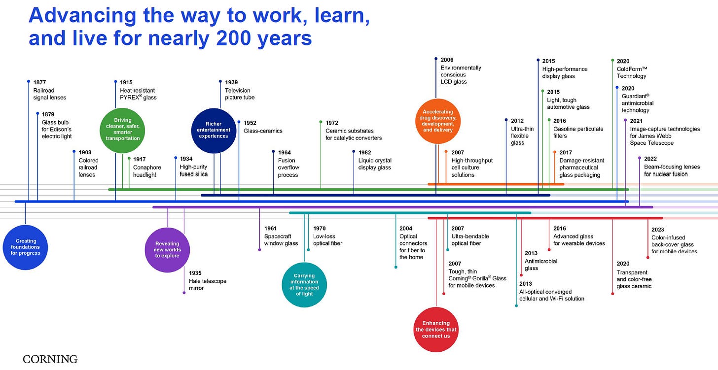
To understand why Corning can re-emerge in the AI era, it helps to zoom out and look at its long arc of reinvention:
19th–early 20th century: industrial glass and precision manufacturing DNA.
Corning’s early growth came from specialty glassmaking, where consistency, purity, and thermal control mattered as much as chemistry. This was not commodity glass; it was process mastery—the kind of capability that later becomes transferable to optical-grade materials.
Early–mid 20th century: laboratory and household glass as a scaled “materials product.”
Corning pioneered glass innovations that entered everyday life, including heat-resistant cookware glass (Pyrex) and later durable consumer glass lines—examples of how the firm repeatedly turned advanced materials into mass production. This matters because the hard part wasn’t the idea—it was the repeatable manufacturing.
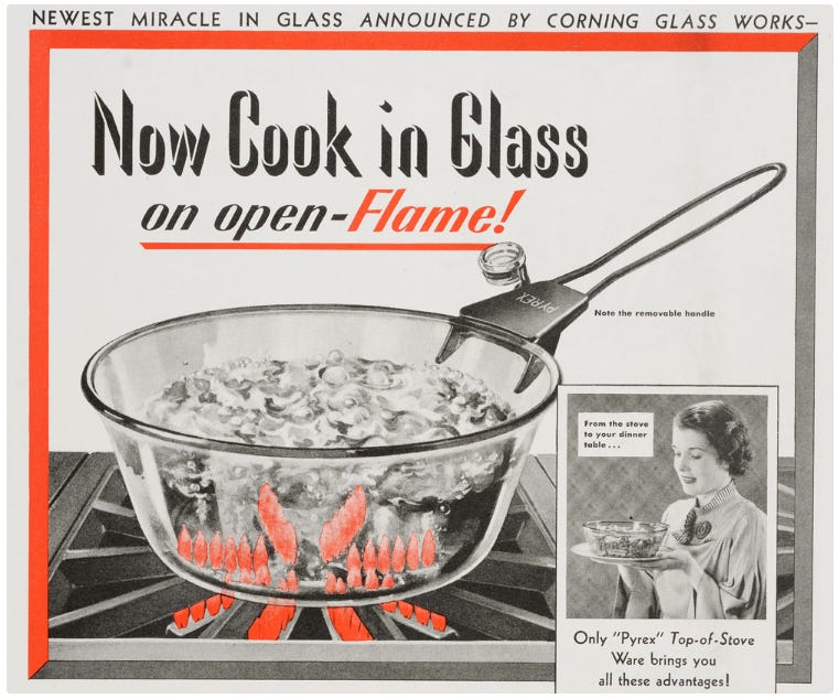
An ad for Pyrex “Top-of-Stove” ware from 1936 shows the flames through the pan’s clear glass. Courtesy the Corning Museum of Glass.
Late 20th century: the decisive pivot—optical fiber becomes a long-duration bet.
In 1970, Corning developed low-loss optical fiber suitable for long-distance communications, widely regarded as a foundational milestone for modern fiber-optic networks. This move repositioned Corning from “glass products” to telecom infrastructure—a market with brutal cyclicality but enormous long-run compounding.
1990s–early 2000s: telecom boom, then collapse—Corning pays the price for being early.
During the internet buildout, optical fiber demand surged—then the dot-com/telecom bubble imploded. After the 2001 crash, Corning’s share price reportedly collapsed from around ~$100 to near $1, reflecting a violent reset of expectations and capacity. For years afterward, Corning’s fiber-related business was treated as a structural problem rather than an asset.
2000s–2010s: diversification through display and mobile glass (the “second engine”).
While telecom was recovering slowly, Corning expanded in other glass categories that benefited from secular growth, notably display glass and strengthened cover glass for smartphones. This period is important because it helped Corning survive the fiber winter without abandoning the optical roadmap.

2001–2020s: the unpopular division that refused to die.
Even as Wall Street repeatedly pushed for Corning to shrink or exit parts of its fiber exposure, the company continued to invest in know-how, process improvements, and manufacturing readiness—treating fiber not as a quarterly P&L story but as a physics-backed inevitability. In hindsight, Corning was essentially preserving an option on the moment when copper could no longer scale.
That moment arrived with AI.
As generative AI forced data centers into unprecedented east–west traffic, bandwidth density, and power constraints, the economics flipped. The “old” fiber business—once criticized for weak returns—suddenly looked like strategic infrastructure. Before the AI wave, much of the industry could still rationalize copper in many internal links; with AI clusters, the copper roadmap runs into hard limits on loss, heat, and power per bit, making optical pathways increasingly unavoidable.

So Corning’s recent repositioning is not a random pivot into AI. It is the culmination of a long cycle: a company that built expertise in ultra-precise glass processing, then placed a decades-long bet on photon-based communication, endured the post-bubble collapse, and finally re-entered the spotlight when AI made high-speed optical connectivity a first-order constraint again. In that sense, Corning did not “become an AI company.” It became an AI-era essential supplier—because the infrastructure finally caught up with the physics that Corning had been betting on all along.
Core takeaway:Corning’s advantage is not simply “glass.” It is the ability to industrialize extremely demanding materials at scale—then wait long enough for the world to be forced into needing them.
With the launch of ChatGPT by OpenAI in late 2022, global demand for AI compute surged

Source: Lightmatter
—and Corning’s long-term investments finally reached a “harvest moment,” where years of accumulation translated into rapid payoff. As tech giants raced to expand AI data centers, fiber-optic demand spiked sharply. From 2023 onward, Corning’s fiber shipments and revenue climbed significantly, and its share price more than tripled over roughly two years. In early 2026, social media giant Meta announced a multi-year fiber supply agreement with Corning worth up to US$6 billion, aimed at supporting Meta’s AI data-center buildout. Corning also disclosed that it is in discussions with multiple major technology companies regarding similar large, long-term supply contracts.

Meta Arizona - Mesa Data Center
Meta establishes ‘Meta Compute,’ plans multiple gigawatt-plus scale AI data centers
Together, these developments have elevated Corning into a “critical hub” of AI-era infrastructure.
This article, SemiVision will analyze how Corning leveraged its technical strengths to complete this strategic repositioning and become an essential enabler of AI data centers and high-speed connectivity. From both an industry and technology perspective, it focuses on:
The differences between optical fiber and copper in high-speed data transmission, and the bottlenecks—and inflection points—created by the AI wave
The current status, trajectory, and Corning’s positioning in Co-Packaged Optics (CPO)
Corning’s core manufacturing moat and competitive advantages, including comparisons with key peers
How Corning maintained commitment through extended loss-making periods and then scaled rapidly as the AI era arrived
Corning’s recent financial performance, stock-price dynamics, and the tangible impact of accelerating AI-related capex on its business.
Below we will share,
Optical Fiber vs. Copper: Physical Characteristics, Bottlenecks, and Inflection Points in High-Speed Data Transmission
Co-Packaged Optics (CPO): A Future Path to Resolving Data Center Bottlenecks
The Role of Glass in Advanced Packaging
Why Glass Matters in Advanced Packaging
Corning’s Vision for Co-Packaged Optics (CPO): Enabling Next-Generation AI Data-Center Connectivity
Intel Foundry’s Advanced Packaging Roadmap: From 2D to 3D Hybrid Bonding
Core Technologies and Competitive Advantages: Corning’s Manufacturing Moat and Peer Comparison
Corning’s Manufacturing Moat: How Glass, Optics, and Vertical Integration Power the AI Infrastructure Era
Corning’s Long-Termism Rewarded: Losses Endured, an AI-Era Breakout Achieved
Synthesis and Outlook
Viewpoint from SemiVision
Optical Fiber vs. Copper: Physical Characteristics, Bottlenecks, and Inflection Points in High-Speed Data Transmission


2025年1月22日
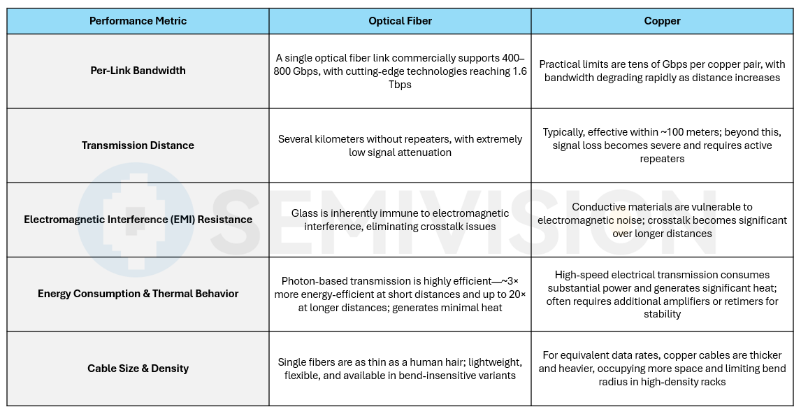
Historically, short-reach connections inside enterprise and cloud data centers relied heavily on copper cabling, largely because of its lower upfront cost and compatibility with legacy equipment. However, as modern AI workloads drive exponential growth in bandwidth and throughput requirements, the technical limitations of copper have become increasingly apparent. In practice, copper cables can function adequately within approximately 100 meters, but beyond that range, signal attenuation and crosstalk interference rise sharply. At high frequencies and data rates, copper transmission efficiency degrades further, requiring power-hungry signal amplifiers or retimers to compensate for losses—devices that also generate substantial heat.
These constraints are especially severe in high-density AI data center environments, where hundreds or thousands of copper cables are interwoven within a single server rack. Such dense copper layouts not only consume physical space and increase routing complexity, but also exacerbate resistive heating, driving up rack temperatures and, in turn, cooling and energy costs .

By contrast, optical fiber is made from extremely high-purity glass. Although its core is as thin as a human hair, it can carry exceptionally high-bandwidth optical signals. Today’s commercial optical links can readily deliver 400–800 Gbps of stable throughput, while more advanced optical interconnect technologies are already reaching 1.6 Tbps-class transmission rates, often over distances measured in kilometers rather than meters. Signal attenuation in fiber is extremely low: a single fiber can transmit data over several kilometers with minimal degradation, whereas copper links often require intermediate amplification after only a few tens of meters.
Optical fiber is also inherently immune to electromagnetic interference, allowing multiple fibers to operate in parallel without mutual crosstalk. As a result, there is no need for the extensive shielding and interference mitigation that copper systems require. From an energy and thermal-management perspective, the advantages of optics are even more pronounced: because optical transmission does not rely on electrical current flow, it generates virtually no heat, making it far more energy-efficient than copper-based connections that depend on high-current drivers.
For these reasons, optical fiber has become the backbone of next-generation data center networks. According to EE Times, roughly 85% of new internal backbone connections in hyperscale data centers now use optical fiber rather than copper, and the rise of generative AI is making this transition effectively irreversible.
In AI data centers, the bottlenecks and inflection points created by these differences have already begun to surface. A representative example can be found in Meta’s large-scale data center in Dallas, Texas. In 2018, Corning CEO Wendell Weeks personally visited the site and observed that neither traditional copper cabling nor existing generations of optical fiber products were sufficient to meet the explosive internal connectivity demands of modern data centers. Tens of thousands of servers and accelerators required high-speed interconnection, and the surge in east–west traffic rapidly elevated network bandwidth to a bottleneck on par with GPU compute capacity itself.
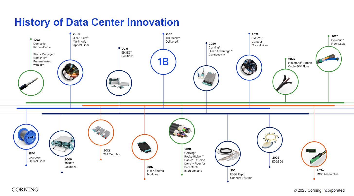
Over the following years, Corning’s engineers developed multiple classes of indoor, high-speed interconnect fibers and ultra-high-density cables that successfully addressed these challenges. These included single-mode fibers with exceptional bend insensitivity, as well as rollable ribbon cable technology capable of packing up to 3,456 fiber cores into a 2-inch diameter conduit, dramatically increasing fiber density per duct.
The inflection point created by the AI wave materialized rapidly in the years that followed. With OpenAI’s launch of ChatGPT igniting an explosion in AI applications, major technology companies began expanding data centers at an unprecedented pace. Between 2023 and 2025, the compute capacity of newly commissioned hyperscale data centers grew at an estimated ~35% annual rate, necessitating the deployment of massive volumes of high-speed interconnects. The east–west traffic required for AI training and inference far exceeds that of traditional cloud workloads: thousands of GPUs must operate in tightly synchronized, low-latency configurations, driving internal optical connectivity demand to more than ten times that of conventional cloud data centers.
For example, a single NVIDIA DGX SuperPOD rack containing 72 GPUs requires roughly two miles of cabling to interconnect its internal components. At an even larger scale, Meta’s planned ultra-large AI data centers—such as the proposed Hyperion campus, designed to house up to 1.3 million GPUs—are estimated to require more than 36,000 miles of optical fiber to interconnect all compute nodes. As a result, network capacity has emerged as one of the most critical bottlenecks in AI infrastructure, alongside compute and power.
Companies such as Microsoft have even warned of a potential future “networking wall”—a scenario in which sufficient GPU compute resources exist, but network bandwidth is inadequate to keep them fully utilized. This dynamic has elevated optical fiber to a strategic position: long regarded as a low-margin commodity, fiber has become a critical resource that cloud service providers are racing to secure. Meta’s US$6 billion long-term supply agreement with Corning is a clear example, reflecting efforts to lock in capacity and co-design specialized fiber solutions to ensure supply stability over multiple years. Other hyperscalers, including Microsoft, are widely expected to pursue similar arrangements .
For Corning, this shift represents a strategic turning point for a business that had long been viewed as mature and cyclical. Optical fiber has transitioned from a telecom-era infrastructure product into one of the most indispensable components of the AI era, with both pricing and demand moving upward in tandem. Industry analysts have described fiber as a “silent dependency that scales nonlinearly with AI cluster size”—the larger the AI data center, the faster the required volume of optical interconnects multiplies. Looking ahead, it is increasingly clear that every AI super-scale data center will be densely woven with fine yet essential glass pathways, forming the “neural network” that physically underpins the age of artificial intelligence.
Co-Packaged Optics (CPO): A Future Path to Resolving Data Center Bottlenecks
In today’s data centers, optical fiber is primarily used for rack-to-rack data transmission, while short-reach connections within servers or racks are still largely handled by copper interconnects and electrical signaling. In practice, this means that when data arrives at a server or switch via optical fiber, it is typically converted back into an electrical signal at the front panel, and then routed through internal copper traces to the processor or switching ASIC .

As AI computing performance accelerates, this short-distance copper segment has emerged as a new bottleneck. Even over distances of just a few meters—or in some cases only a few tens of centimeters—signal quality can degrade significantly, requiring additional driver or retimer chips to compensate for losses. This not only increases power consumption but also generates additional heat. Traditionally, each switching ASIC is connected to front-panel optical modules through high-speed PCB traces. At data rates above 200 Gbps, these electrical paths can incur signal losses exceeding 20 dB, necessitating the use of power-hungry DSP chips, often consuming tens of watts, to restore signal integrity.
When thousands of optical modules are populated across a single rack, the power consumption of the optical interconnect subsystem itself can rival—or even exceed—that of the compute hardware, creating severe challenges in thermal management and long-term reliability.
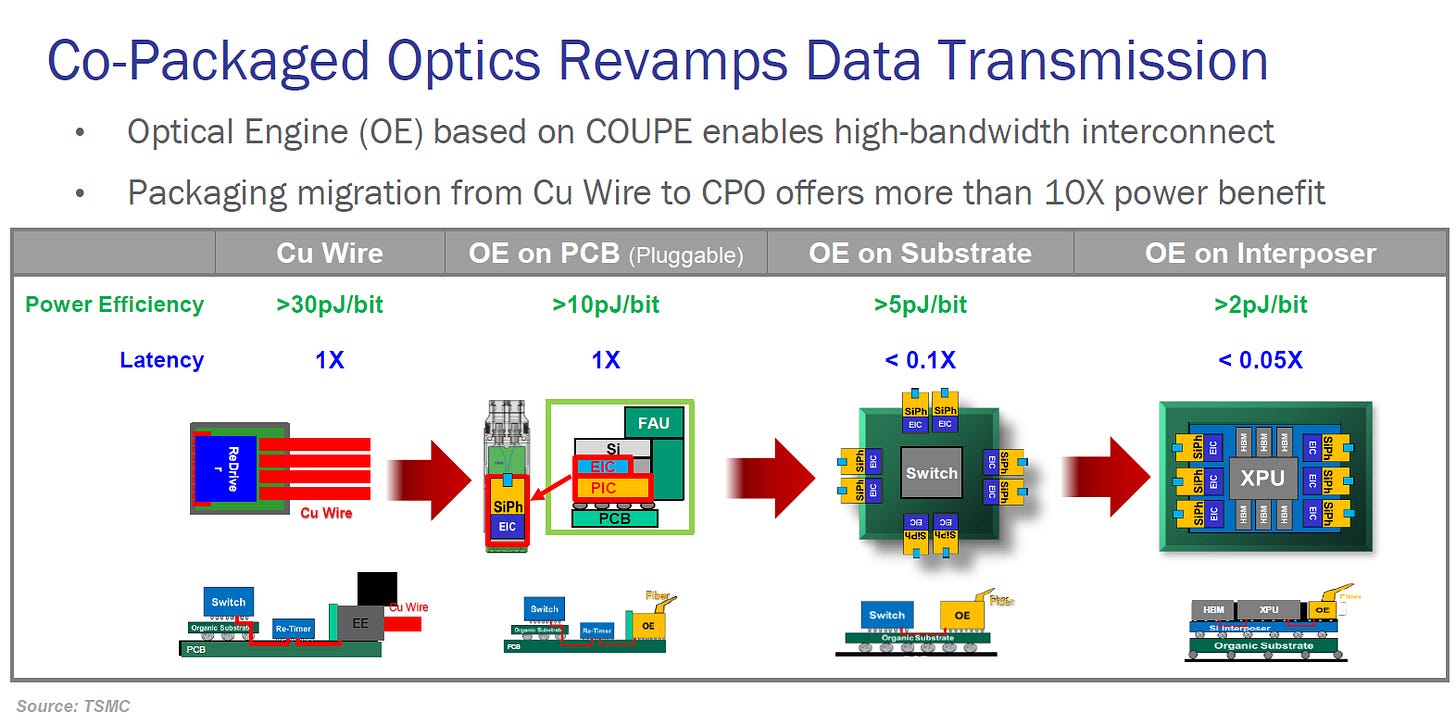
Co-Packaged Optics (CPO)technology is designed specifically to address the bottlenecks described above. The core idea of CPO is to integrate optical components directly within the server or switch package, in close proximity to the processor or switching ASIC, so that data is transmitted in optical form immediately from the point it exits the chip. In other words, the domain of optical fiber is extended from between racks into the chassis and even the chip/package level, with optical–electrical conversion occurring only near the GPU, CPU, or switch ASIC.
By eliminating the traditional copper distance between the chip and the optical module, CPO places the optical interface directly at the silicon edge, dramatically reducing high-speed I/O loss and power consumption.
As Claudio Mazzali, Senior Vice President at Corning, explains: “By co-packaging optical devices with the chip, we can significantly reduce power consumption, increase data transmission rates, and free up valuable I/O real estate on the silicon” .
Experimental data shows that a1.6 Tbps optical port using CPO can reduce power consumption from roughly 30 watts in conventional designs to less than 10 watts.
For data centers, this represents a triple gain in performance, cost efficiency, and energy efficiency. A single AI server rack often contains nearly two miles of copper cabling interconnecting hundreds of chips. As link speeds climb into the hundreds of gigabits per second, copper links must rely on expensive active retimers (signal amplification and reconditioning devices) to sustain transmission quality, turning the entire rack’s cabling infrastructure into a power-hungry and failure-prone weak point. CPO addresses this by eliminating these lossy copper links, allowing data to remain in the optical domain along the entire path, thereby reducing energy waste and signal latency.
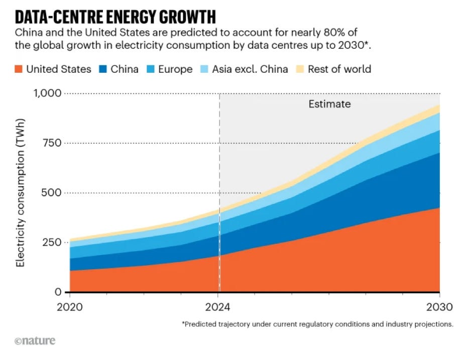
Industry estimates suggest that CPO can lower per-unit optical interconnect costs by approximately 40% while cutting interconnect power consumption by more than 50%. At a time when energy is becoming one of the dominant cost drivers in data center operations—U.S. Department of Energy projections estimate that data centers could account for 6.7–12% of total U.S. electricity consumption by 2028 —such levels of energy savings are critical to the long-term sustainability of AI infrastructure.
At present, CPO technology is still in the early stages of industrialization. In March 2025, NVIDIA announced the launch of its first switch chip with built-in co-packaged optics, integrating silicon photonic transceivers directly into the switch ASIC package. This product marked a critical milestone, signaling CPO’s transition from laboratory research toward commercial deployment. Beginning in 2025–2026, more switches and servers are expected to gradually adopt CPO architectures, incrementally breaking through the bandwidth and energy-efficiency limitations of traditional pluggable optical modules.
As a leader in optical fiber technology, Corning has been actively investing in innovation within the CPO ecosystem. Mike O’Day, General Manager of Corning’s Optical Communications business, has noted that the rise of generative AI places significantly higher demands on internal data center networks, and that Corning aims to use CPO technologies to“make the data center’s neural network smarter”.

Leveraging decades of expertise in glass and optical materials, Corning has developedFlexConnect, a short-reach, bend-insensitive optical fiber specifically designed for CPO applications. This single-mode glass fiber is optimized for ultra-short-distance, high-bandwidth, low-loss connections within CPO packages. Serving as a bridge between chips inside the server and the external optical “highways” of the chassis, FlexConnect is engineered to withstand the severe bending and mechanical stresses present within tightly integrated packages.

In addition, Corning has combined its fiber products with complementary connectors and optical transceivers into the GlassWorks AI solution, positioning it as a one-stop offering for both intra–data center and inter–data center networking requirements.
AGC: Integrating Glass Solution in Advanced Packaging

2025年9月16日
The Role of Glass in Advanced Packaging
Beyond optical fiber interconnects, Corning is also leveraging its strengths in glass materials science to develop Glass Core substrate technology for advanced semiconductor packaging. Glass Core substrates are fabricated using specialized glass fusion processes that deliver exceptional thermal stability and surface flatness, enabling the formation of through-glass vias (TGVs) for vertical interconnects between chip layers.
Glass has emerged as a critical material platform in advanced semiconductor packaging, enabling higher integration density, better thermal and mechanical stability, and new system architectures that are increasingly required by AI and high-performance computing (HPC) applications. Broadly, glass is used in advanced packaging in two major roles: as a process enabler (temporary carrier) and as a structural integration platform (glass core substrate).

Source: Corning
- Glass as a Process Enabler: Temporary Glass Carriers
Temporary Glass Carriers for Wafer Thinning
In advanced packaging flows—particularly 2.xD and 3D integration—silicon wafers must be thinned to tens of microns to enable high-density vertical interconnects such as TSVs. Temporary glass carriers are widely used to support silicon wafers during thinning, handling, and processing.
Key advantages of glass carriers include:
Excellent flatness and dimensional stability, reducing wafer warpage during thinning
High thermal resistance, compatible with high-temperature process steps
Optical transparency, enabling alignment and inspection from the backside
Once processing is completed, the glass carrier is removed, making this aconsumableuse of glass.
- Temporary Glass Carriers for RDL Formation and Assembly
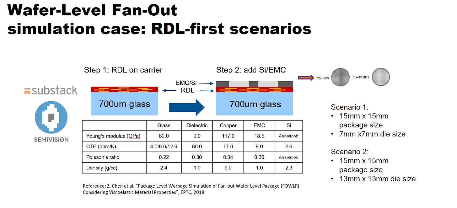
Glass carriers are also used during redistribution layer (RDL) formation and advanced assembly steps in fan-out packaging, both at the wafer level and panel level.
In this context, glass enables:
Fine-line RDL patterning due to high surface smoothness
Improved yield and dimensional control for large-area fan-out structures
Scalability from wafer-based to panel-based manufacturing
As fan-out technologies move toward panel-level processing to reduce cost and increase throughput, glass carriers play an increasingly important role.
Source: Corning
- Glass as a Structural Platform: Glass Core Substrates
Glass Core as a New Integration Substrate
Beyond temporary use, glass is evolving into a permanent structural material in advanced packaging through glass core substrates. In this application, glass replaces traditional organic substrates as the core material of the package.
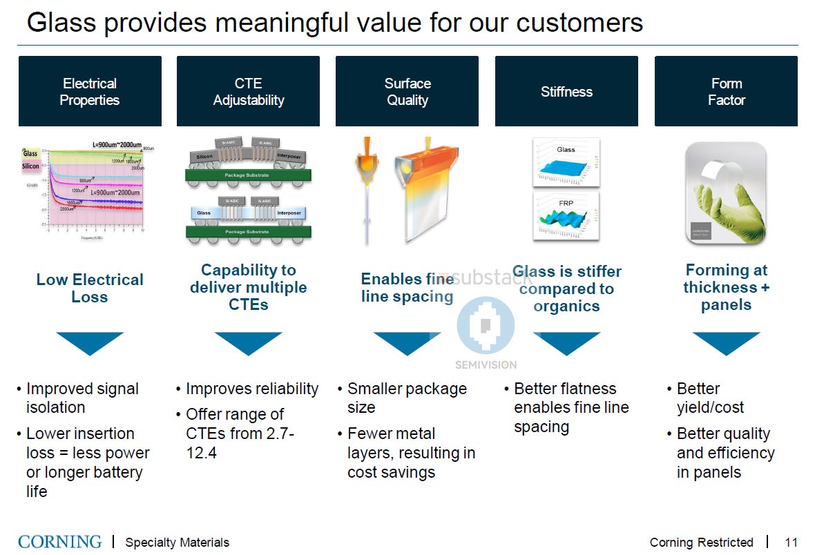
Glass core substrates offer several structural and electrical advantages:
Low and tunable coefficient of thermal expansion (CTE), improving compatibility with silicon
High stiffness and low warpage, especially important for large, multi-die packages
High electrical insulation, reducing signal loss and crosstalk
Capability to form through-glass vias (TGVs) for high-density vertical interconnects
These properties make glass core substrates particularly attractive for 2.xD interposers and future 3D heterogeneous integration platforms.

Source: Corning
Enabling Future Architectures: Optical and Power Integration
Glass core substrates also open the door to next-generation integration concepts, including:
Embedded optical waveguides for optical I/O and co-packaged optics (CPO)
Integrated power delivery structures with improved stability and lower loss
Large-area substrates for chiplet-based architectures and AI accelerators
In this sense, glass is no longer just a supporting material—it becomes a system-level enabler.
Why Glass Matters in Advanced Packaging
Across fan-out, 2.xD, and 3D architectures, glass plays a dual and increasingly strategic role:
As a temporary carrier, it enables aggressive wafer thinning, fine-pitch RDL, and scalable panel-level manufacturing.
As a core substrate, it provides a new integration platform that supports higher density, better thermal-mechanical performance, and future optical-electrical convergence.
As advanced packaging shifts from a “connectivity problem” to a system integration problem, glass is emerging as one of the few materials capable of scaling with the demands of AI, HPC, and heterogeneous integration.
Compared with conventional organic package substrates, glass substrates offer tunable coefficients of thermal expansion and significantly reduced warpage in high-density, multi-die packaging, thereby improving both interconnect density and long-term reliability. Looking ahead, this technology has the potential to converge with CPO architectures: optical waveguides could be directly integrated into the glass substrate, allowing optical signals to propagate within the chip package itself and enabling seamless electro-optical integration in high-speed modules

Corning’s proprietary glass fusion process is particularly well suited to manufacturing such substrates, ensuring dimensional stability, ultra-flat surfaces, and precise via formation. As Mazzali has emphasized, Corning has been deeply invested in optical fiber and glass processing technologies for decades; what is happening now is simply the translation of these mature capabilities into the emerging demands of optical interconnects.
Intel Foundry’s Advanced Packaging Roadmap: From 2D to 3D Hybrid Bonding
As system complexity accelerates in the AI and high-performance computing era, advanced packaging has become a primary driver of performance, power efficiency, and integration density. Intel Foundry’s packaging roadmap illustrates a clear evolution—from traditional 2D assembly to 2.5D integration and ultimately 3D hybrid bonding—positioning packaging as a strategic enabler rather than a backend afterthought.

At the foundation is FCBGA/FCLGA technology, built on ~100µm bump pitch and optimized for large substrates up to 120x120mm. These platforms support high-volume manufacturing and cost-efficient system integration, forming the backbone of mainstream compute products.
Moving into 2.5D, Embedded Multi-die Interconnect Bridge (EMIB) technology significantly increases bandwidth and power efficiency. With bump pitch scaling from 55µm down to 25µm and TSV support, EMIB enables large form-factor integration beyond reticle limits. This architecture has shipped since 2017 and continues to scale toward larger reticle equivalents.
Foveros extends integration into true 3D stacking. Initially introduced with bump pitch scaling from 36µm to 25µm, Foveros supports wafer-level packaging with silicon interposers. Foveros Direct pushes this further through direct copper-to-copper hybrid bonding at sub-10µm pitch, delivering high-density interconnects, lower resistance, and superior power-per-bit efficiency.
Looking ahead, Intel is investing in glass core substrates and co-packaged optics. Glass substrates promise improved power delivery and signal integrity at high speeds, while optical integration addresses the bandwidth and energy challenges of next-generation AI infrastructure.
Together, these technologies signal a decisive shift: packaging is no longer secondary—it is central to scaling compute performance in the coming decade.
Heterogeneous Integration: Intel Foundry’s Substrate Scaling Strategy and the Semiconductor Industry Transformation

In an era of rapid evolution for the semiconductor industry, heterogeneous integration has emerged as the key pathway beyond Moore’s Law, enabling chips with different process nodes, materials, and functions to work together within a single package — thereby improving performance, reducing power consumption, and optimizing cost. The blueprint presented by Intel Foundry at the 2026 NEPCON conference, titled “Scaling Substrate for Heterogeneous Integration into the Future,” precisely captures the core of this trend, positioning the substrate as the central hub of integration.
The technical architecture illustrated in the figure spans from large-format packaging (such as 300 mm wafer-level panel processing), to high-precision embedding of chip-to-chip bridges, and extends to high-density routing technologies — including advanced fine-line patterning, fine vias, through-glass vias (TGV), high-bandwidth HSIO with advanced dielectric materials and smooth Cu/barrier layers — all converging toward one goal: achieving finer interconnects and truly modular system design.
The depth of this strategy lies in its direct response to critical industry pain points. Traditional silicon-based scaling is increasingly constrained by physical limits and yield challenges. Intel’s approach mitigates these issues through fine-pitch assembly, planar bumping & buildup layers, and advanced substrate technologies that elevate packaging precision to near-front-end levels. Notably, the SiFab backend-like infrastructure shown in the figure aims to bring front-end-like yield and control to advanced packaging — a prerequisite for meeting the extreme demands of AI and high-performance computing (HPC), such as integrating co-packaged optical interconnects for massive data movement and incorporating sophisticated power delivery (integrated or discrete) to optimize energy efficiency.
From an industry perspective, Intel’s substrate scaling vision signals a major reshaping of the supply chain. Compared with TSMC’s CoWoS or Samsung’s I-Cube, Intel emphasizes an open Foundry model, which could lower entry barriers and foster broader ecosystem collaboration. However, significant challenges remain: material innovations (e.g., glass substrates replacing organic ones) must overcome issues of coefficient of thermal expansion (CTE) mismatch and long-term reliability, while geopolitical risks (such as U.S.–China trade tensions) continue to threaten supply-chain stability.
Looking ahead, with the rise of quantum computing, 6G communications, and next-generation AI workloads, heterogeneous integration will drive the semiconductor industry from single-die dominance toward system-in-package modularity. Market forecasts suggest the advanced packaging sector could more than double in size by 2030. Yet the decisive factor for success will be the ability to balance aggressive innovation with manufacturability at scale. Intel’s ambitious roadmap will require strong cross-industry collaboration — particularly through open standards like UCIe — to achieve true volume production.
In summary, this is not merely a technology roadmap; it is a declaration of the semiconductor industry’s transition toward modularity and sustainability. It deserves close attention from investors, engineers, and strategists alike.

2025年5月1日
Taken together, CPO is widely viewed as one of the most important evolutionary directions for future data-center network architectures. Once the technology reaches full commercial maturity, it has the potential to eliminate the last remaining electro-optical conversion bottleneck on the server side, allowing data to flow between processor chips and the network entirely in the optical domain, effectively at the speed of light. The active participation of chip leaders such as NVIDIA, combined with coordinated innovation across the supply chain—including companies like Corning—is accelerating the industrialization of CPO. Corning has already begun collaborative research with NVIDIA to evaluate the feasibility of deploying its CPO technologies inside servers.
2025年4月15日
If this model succeeds, every AI server, every high-performance computing cluster, and even every switch could eventually embed Corning’s optical components. In such a scenario, Corning would transition from primarily selling optical cables to supplying core optical building blocks, expanding its addressable market by orders of magnitude. At the same time, Corning’s management remains cautious, emphasizing that large-scale commercialization of CPO will still require sustained technical and cost breakthroughs. Much like the early development of optical fiber, CPO may demand long-term patience and continued investment before its full value is realized.
Corning’s research presents a comprehensive process technology for advanced glass substrates aimed at next-generation co-packaged optics (CPO) used in AI, HPC, and data-center switching applications. The core contribution is the successful integration of cavities and through-glass vias (TGVs) within a single glass substrate, enabling tight co-integration of optical and electrical components while minimizing high-frequency signal loss.
The study demonstrates a combined mechanical processing and HF-based wet chemical etching approach to precisely control cavity geometry, achieving tunable taper ratios between 0.1 and 0.6. This allows reliable die embedding and high-aspect-ratio via formation inside cavities of varying depths. Multiple TGV dimensions were validated, confirming manufacturability across different cavity profiles.
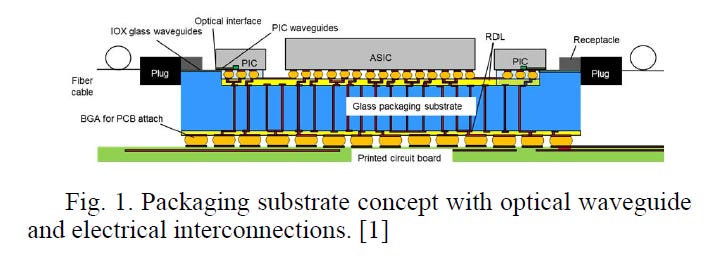
A major innovation lies in redistribution layer (RDL) formation inside deep glass cavities. Corning developed a spray-coated photoresist process, coupled with laser direct imaging (LDI), to overcome the limitations of conventional spin coating on 3D surfaces. This enabled fine Cu electrode patterning with line/space below ~5 µm on cavity floors. Adhesion challenges between copper and glass were addressed using Ti/Cu seed layers and optimized surface cleaning.
Overall, the work establishes glass substrates as a viable, scalable platform for electro-optical integration, offering low dielectric loss, excellent flatness, and high-precision metallization—key enablers for future ultra-high-bandwidth CPO architectures.

2025年4月3日
Weeks has even joked that he has not yet been invited to NVIDIA CEO Jensen Huang’s famous “barbecue and beer gatherings”—a lighthearted way of acknowledging that the collaboration is still in its early stages and that true inclusion will come only after tangible results are delivered. This remark neatly captures the current reality of CPO development: the outlook is highly promising, but meaningful challenges remain. In short, as AI-era data-center networking requirements continue to escalate, optical innovations such as CPO will keep advancing—and Corning’s role in this evolution deserves close attention.

1月29日
Core Technologies and Competitive Advantages: Corning’s Manufacturing Moat and Peer Comparison
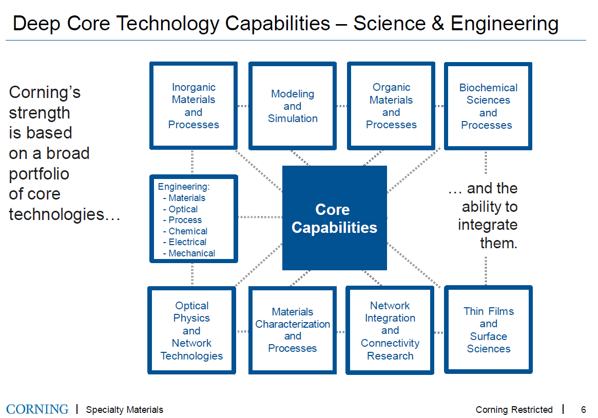
Corning’s successful transformation from a traditional glass manufacturer into a leader in the optical communications industry is rooted in its deep accumulation of core manufacturing technologies and a distinctive, highly vertical integration strategy. First and foremost, in optical fiber production, Corning has led the industry’s technological evolution ever since it successfully drew the world’s first low-loss optical fibers in 1970. Producing high-quality optical fiber requires a series of complex and tightly controlled steps—including glass composition development, optical fiber preform fabrication, high-temperature fiber drawing, coating, and final cable assembly—each of which involves substantial process barriers.
Corning has adopted an approach of“extreme vertical integration,”relying minimally on external suppliers. The company formulates its own glass materials and chemical dopants, designs and builds its own fiber-drawing towers and manufacturing equipment, and develops proprietary fiber coatings and cable-jacket assembly technologies. In other words, from raw materials to production lines to finished optical cable assemblies, Corning maintains firm control over every stage of the value chain.
This near-fully integrated control provides Corning with a critical strategic advantage: the ability to rapidly realign R&D priorities and manufacturing capacity in response to shifting market demand. For example, when Corning identified emerging data-center demand for new classes of optical cables in 2018, it was able to quickly modify production equipment and prototype new products—an execution speed that is extremely difficult for competitors who rely heavily on third-party equipment suppliers to match.
Corning’s materials science depth and process-innovation capability form another critical layer of its competitive moat. At the core of optical fiber lies ultra-high-purity silica glass, and Corning engineers often note with pride that their glass is so pure and transparent that if an entire ocean were filled with it, the human eye could still see the seafloor [76]. This level of purity is the result of industry-leading glass melting and deposition processes that few competitors can replicate at scale.
Corning has also been a pioneer in developing bend-insensitive fibers (such as the ClearCurve series) and ultra-low-loss optical fibers, enabling deployment across a wide range of application environments. For example, in 2023 Corning introduced a new class of ultra-low-loss optical cables specifically designed for high-performance data center applications, underscoring its ongoing commitment to innovation. In the area of high-density cabling, Corning’s rollable ribbon fiber technology allows thousands of fiber cores to be densely packed within a single cable while maintaining sufficient flexibility for installation and routing. Together, these innovations further reinforce Corning’s technological leadership.
Beyond technology itself, talent management and organizational strategy provide Corning with an additional competitive edge. Weeks has repeatedly emphasized what he calls “The Corning Way”—a philosophy under which the company avoids dismantling R&D and engineering teams when shifting strategic direction. Instead, engineers are reassigned to new projects, ensuring that critical knowledge and skills accumulate within the organization over decades. Much of the know-how in optical fiber manufacturing cannot be learned from textbooks; it is built through years of hands-on experience and iterative refinement.
By retaining core teams during downturns, Corning preserves its ability to pivot quickly when opportunities emerge. During the COVID-19 period, the company experienced six consecutive quarters of revenue decline, marking its most severe downturn since the telecom collapse of 2001. Conventional cost-cutting would have involved large-scale layoffs. Instead, Corning chose an unconventional approach: employees accepted a portion of their compensation in stock, allowing the company to weather the downturn together. At the time, Corning retained an estimated 4,000–5,000 more employees than revenue levels would typically justify.
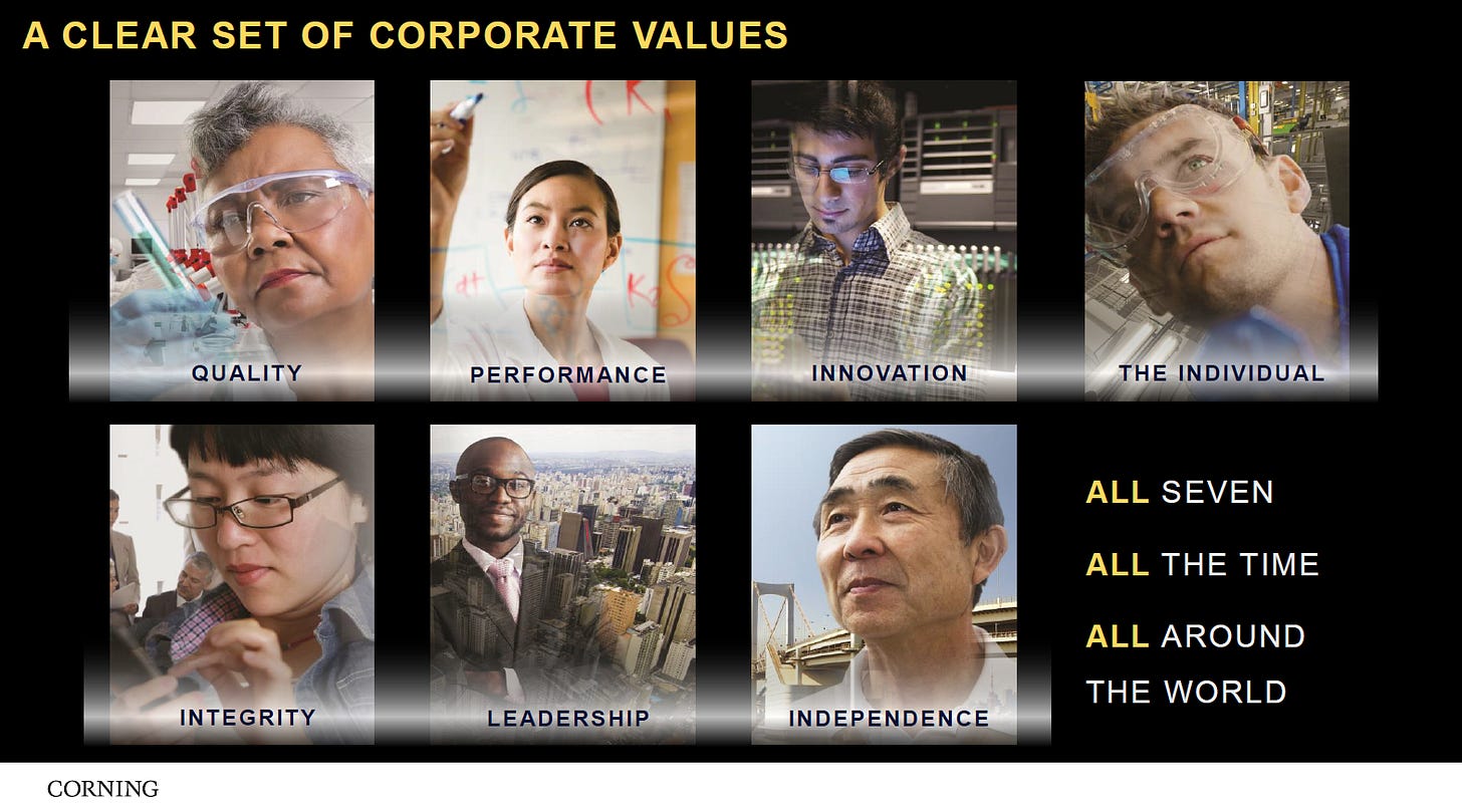
This decision later proved prescient. When AI-driven demand surged, Corning already had a deep bench of skilled workers and ready capacity, enabling it to ramp production immediately—without the long rebuilding cycle that often follows mass layoffs. By contrast, competitors relying heavily on labor-intensive outsourcing faced shortages of skilled labor or insufficient capacity and risked missing the window of opportunity. Corning’s approach illustrates the value of long-termism, strengthens supply stability, and further enhances its attractiveness to large, strategic customers.
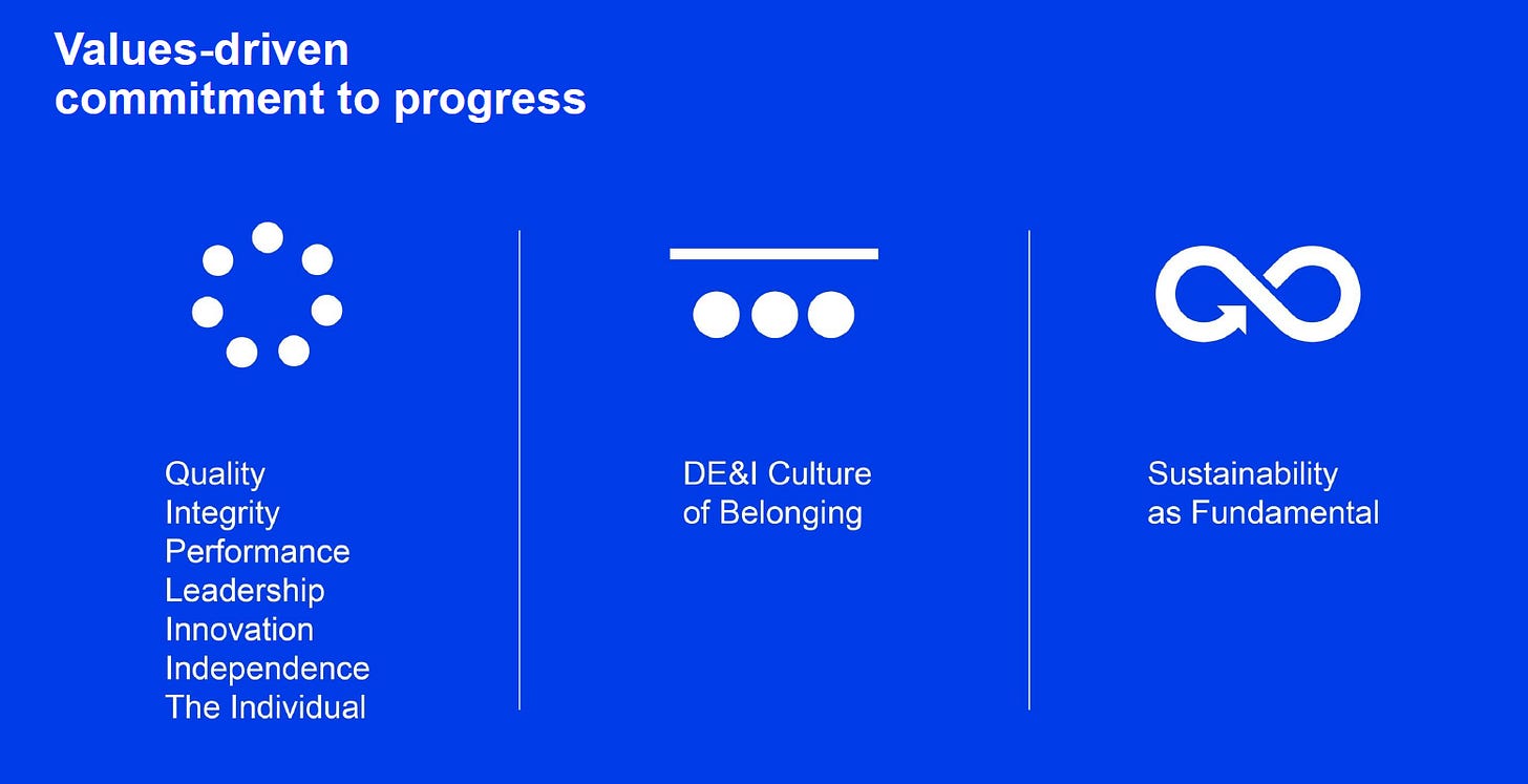
Corning’s Manufacturing Moat: How Glass, Optics, and Vertical Integration Power the AI Infrastructure Era
From an industry competition perspective, the global optical fiber and cable market exhibits a structure characterized by multiple strong players with moderate concentration. According to market report, measured by 2025 revenue, the world’s top five integrated fiber suppliers—defined as companies that both produce fiber preforms and manufacture optical cables—collectively account for roughly 45% of the global market. This group includes Corning, CommScope, Lightera, Prysmian Group, Sumitomo Electric, Furukawa Electric, OFS, as well as China’s YOFC…etc.

Among these players, Corning is the only U.S.-based supplier, with an estimated 8–10% global market share (some estimates place its 2023 share at approximately 10.4%) . Prysmian Group is the European leader; following its 2018 acquisition of U.S. communications cable maker Draka, Prysmian significantly expanded its scale and now holds an overall market share of roughly 15%, slightly higher than Corning’s. Sumitomo Electric and Furukawa Electric represent Japan’s two major fiber manufacturers: Sumitomo is known for its strength in VAD (Vapor-phase Axial Deposition) technology, while Furukawa, through its acquisition of U.S.-based OFS (originating from Bell Labs’ fiber optics business), commands advanced North American fiber technologies. Each holds a global market share of several percentage points. Chinese suppliers such as YOFC and Hengtong dominate the domestic Chinese market and are increasingly expanding internationally, benefiting from economies of scale and government support.
Corning’s competitive advantage relative to its peers lies primarily in its speed of technological innovation and leadership in high-end markets. The company was among the first to respond to AI data centers’ demand for new classes of optical cables, delivering performance and customization that meet the most stringent requirements of customers such as Meta and Microsoft. Corning’s vertically integrated operating model also allows it to secure internal supply during periods of raw-material tightness. For example, in the second half of 2025, North America experienced a shortage of optical fiber glass preforms, extending lead times at some suppliers to nearly a year. Market reports suggested that Corning temporarily halted external preform sales in order to prioritize its own cable production.
In addition, as the U.S. government pushes for localization of critical communications infrastructure supply chains, Corning’s substantial advanced manufacturing footprint within the United States—particularly in the Hickory, North Carolina region—has become a significant differentiator. For hyperscale data center operators whose primary deployments are in the U.S., this domestic capacity carries strong strategic appeal. By contrast, many of Corning’s major competitors, including Prysmian and Sumitomo, maintain the bulk of their production capacity in Europe or Japan/Southeast Asia, which may be less convenient when serving large U.S.-based hyperscalers.
As these dynamics play out, Corning has increasingly been viewed as one of the key beneficiaries of “AI infrastructure localization”, aligning closely with U.S. industrial policy priorities and attracting heightened attention from major cloud and AI service providers.

Of course, competitors across the industry are also accelerating their innovation efforts. Among emerging technologies, Hollow-Core Fiber (HCF) represents one of the most significant breakthroughs in optical fiber in recent years. HCF guides light through a hollow, air-filled core, allowing propagation speeds close to that of light in vacuum—approximately 30% faster than conventional solid-glass fiber—while also reducing nonlinear effects and latency . Loss levels for hollow-core fiber have now fallen to around 0.28 dB/km, demonstrating strong potential for high-bandwidth, long-distance transmission.

Microsoft invested in and acquired the UK-based hollow-core fiber startup Lumenisity in 2021–2022, and in 2025 announced a collaboration with Corning under which Corning’s North Carolina facilities would mass-produce Microsoft’s hollow-core fiber for low-latency data center interconnects. This partnership highlights Corning’s open and collaborative stance toward frontier technologies, ensuring it does not miss the next major technology wave. At the same time, Prysmian Group has partnered with startup Relativity Networks to build a hollow-core fiber manufacturing facility in the Netherlands, seeking to secure a position in this emerging field.
In the indoor cabling segment, competitors such as Furukawa and Sumitomo Electric have also introduced their own high-density, bend-insensitive fiber products. Looking ahead, competition among leading suppliers is increasingly likely to concentrate on high-end and specialized applications—for example, who can be first to commercialize CPO-ready internal interconnect fibers, or who can deliver ultra-low-latency fiber solutions tailored for financial trading or AI workloads. With its deep R&D capabilities and close collaboration with end customers, Corning currently holds a first-mover advantage in these high-barrier markets, but sustained leadership will require continued investment and innovation.
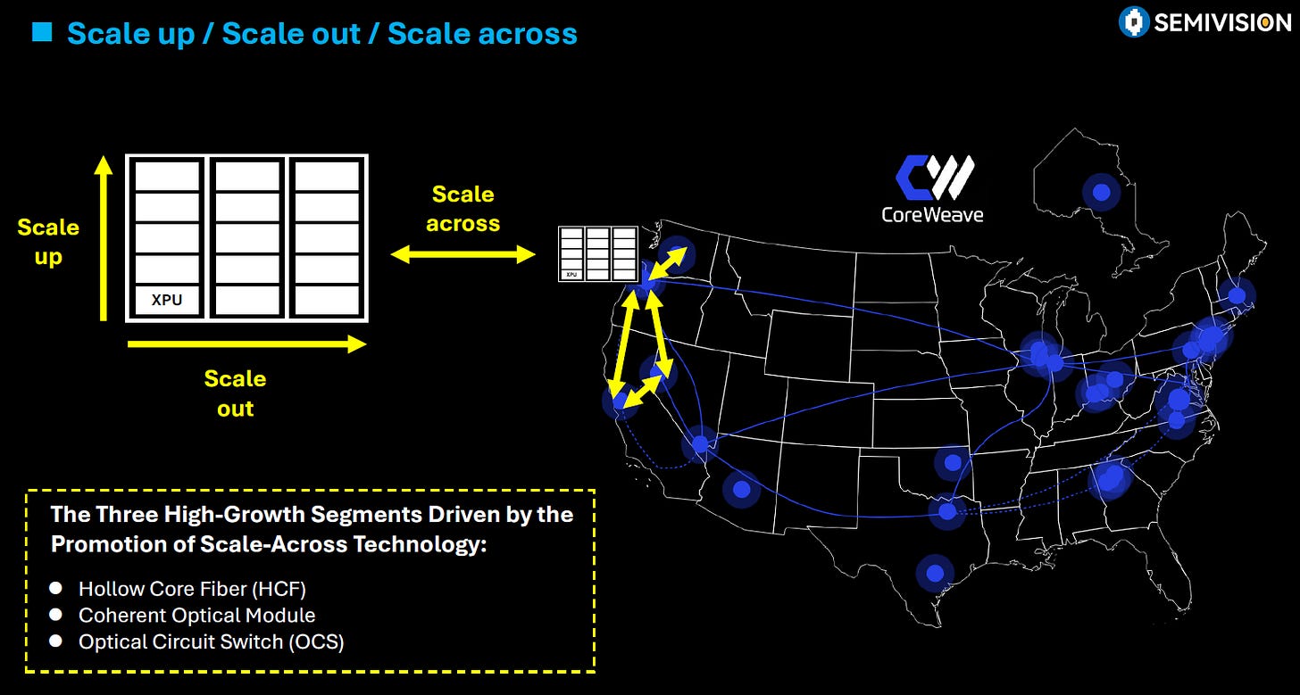
Overall, Corning’s competitive advantages stem from a unique combination of industry-leading materials and process innovation, extreme vertical integration that enables agile manufacturing and tight quality control, a deep reservoir of talent and technical know-how accumulated through long-termism, and domestic production capacity that aligns closely with evolving market and policy trends. Together, these strengths have positioned Corning at the forefront of competition in the AI era. Looking ahead, Corning must remain vigilant as competitors advance in specific niches, while continuing to leverage its core advantages to expand into new growth opportunities.
Long-Termism Rewarded: Losses Endured, an AI-Era Breakout Achieved
The dramatic turnaround of Corning’s optical fiber business is widely regarded as a textbook example of industrial long-termism in a traditional manufacturing company. At the height of the internet boom around 2000, Corning’s market capitalization—driven largely by optical fiber—once approached USD 100 billion. When the bubble burst, demand collapsed, fiber prices plunged, and the company was forced into layoffs and deep losses [98]. For nearly two decades thereafter, the optical fiber market remained oversupplied and fiercely competitive, leaving Corning’s fiber division operating at a loss or near breakeven for extended periods. Many investors and analysts urged the company to divest or shut down what they saw as a “non-core” or low-return business.
Corning’s management, however, held firm in the belief that optical fiber would eventually regain strategic importance. Instead of retreating, the company continued to invest in R&D and maintain capacity through the downturn. As The Wall Street Journal later observed, Corning’s journey became a master class in industrial patience and long-term commitment.
The inflection point began in 2018, when Corning identified the coming surge in data center networking demand and moved early to develop new, fit-for-purpose products. The real catalyst arrived in late 2022 with the launch of ChatGPT, which ignited industry-wide urgency for high-speed AI infrastructure. After years of preparation, Corning was ready—with bend-insensitive, small-diameter fiber optimized for data centers, fully utilized fiber plants, and a seasoned engineering workforce.
Orders surged. According to Mike O’Day, head of Corning’s Optical Communications business, demand now exceeds the company’s capacity, with every meter of fiber sold immediately upon production. Meta’s multi-billion-dollar long-term supply agreement announced in August 2023 was only the beginning; Corning has since signed additional contracts with hyperscale customers, effectively locking in capacity for years ahead. Optical fiber has become Corning’s fastest-growing segment.
Had Corning followed Wall Street’s advice and exited fiber years earlier, it would have been impossible to re-enter the market in time to capture the AI wave. As one analyst noted, “If Corning could make more fiber today, it would sell more—demand will exceed supply for a long time”. Indeed, the entire North American fiber industry is now undersupplied, with lead times stretching from the usual two to three months to nearly a year, reminiscent of the peak in 2000. Some industry participants describe AI data centers as “vacuuming up all available fiber capacity” .
Corning’s ability to respond so rapidly also reflects its long-term people strategy. During downturns such as the pandemic, the company chose to retain employees and critical skills, enabling it to ramp production immediately when demand returned after 2023. CEO Wendell Weeks attributes this to measuring success “in decades rather than quarters,” accepting short-term pressure to preserve long-term opportunity. Time and again, Corning chose to double down on its core strengths rather than walk away.
Today, the business once viewed as expendable has become a strategic partner to the global AI ecosystem. From Edison-era light bulb glass to light-speed connections for artificial intelligence, Corning’s story reflects resilience, patience, and the enduring power of long-termism in technological revolutions.
Synthesis and Outlook
Taken together, these developments show that Corning has executed a textbook turnaround in the wake of the ChatGPT- and AI-driven wave. Financial results validate the effectiveness of its transformation: the optical fiber business has shifted from years of losses to a core growth engine, with both revenue and profitability reaching record highs. The sharp rise in Corning’s share price reflects capital markets’ confidence in its future, though elevated valuations also embed high expectations for sustained growth.
Viewpoint from SemiVision
From its origins supplying glass for Edison’s light bulbs, through cathode-ray tubes, cookware, optical fiber, display glass, and now AI infrastructure, Corning’s history repeatedly confirms one lesson: deep investment in core technologies and a long-term value mindset ultimately enable resilience amid shifting market cycles. In the current AI data center wave, Corning has successfully leveraged decades of optical expertise and sustained commitment to capture a renewed moment of growth.
The fundamental advantages of optical fiber over copper in high-speed data transmission ensure that fiber will remain the indispensable “neural network” of AI-era data centers. Over the coming years, continued advances in generative AI, cloud computing, and 5G will further lift global demand for high-speed optical connectivity. At the same time, emerging technologies such as co-packaged optics (CPO) and hollow-core fiber hold the potential to unlock a new efficiency revolution, expanding the addressable market even further. Corning is already active at the forefront of these developments. If CPO and related technologies reach large-scale commercialization, Corning could evolve from primarily a cable supplier into a provider of core data center components, significantly strengthening its strategic position.
Opportunities, however, come with challenges. Corning’s current growth remains closely tied to the intensity of AI infrastructure spending; any slowdown in hyperscaler capital expenditures could temper fiber demand growt. Moreover, maintaining supply–demand balance and managing capacity expansion during a period of exceptional demand will test execution discipline. Still, Corning’s more than 170-year history demonstrates a rare ability to navigate cycles with resilience. In particular, the lessons of the past two decades have reinforced the importance of preparing during peaks and investing through downturns.
Looking forward, Corning is likely to continue adhering to a long-term strategy—leveraging the AI and data-driven era while reinforcing its leadership in high-speed connectivity infrastructure. Through sustained R&D and the convergence of glass science and optical innovation, the company is positioning itself for the next generation of technology platforms. From illuminating the world with Edison’s light bulbs to enabling the flow of light-speed data for artificial intelligence, Corning’s story illustrates a powerful truth:
Traditional industries, when anchored in core strengths and open to innovation, can become leaders in new technological revolutions.
And in the years ahead, this strand of glass—thinner than a human hair—will continue to carry humanity’s expanding data flows, with Corning leaving a lasting imprint on the technological landscape.

2025年12月31日


PreviousNext
TopLatestDiscussions








See all