In Space, Power Is Destiny: Solar Panels and the Future of Satellites
In Space, Power Is Destiny: Solar Panels and the Future of Satellites
- Source: SemiVision
- Author: SEMIVISION
- Published: 2026-02-09T16:12:33+08:00
- URL: https://tspasemiconductor.substack.com/p/in-space-power-is-destiny-solar-panels In Space, Power Is Destiny: Solar Panels and the Future of Satellites


In Space, Power Is Destiny: Solar Panels and the Future of Satellites
Original Article By SemiVision Research

Feb 09, 2026
∙ Paid
Why Solar Panels Are Essential for Space Satellites

When discussing power systems for space satellites, the question is no longer whether solar energy should be used, but rather how well it can be engineered. In the space environment, solar power is not an option—it is the only viable primary energy source for long-duration satellite missions.

2月9日
Solar Power Is the Only Scalable Power Solution in Space
From a system-level perspective, the power subsystem is one of the most valuable and mission-critical components of a satellite. In a typical satellite cost structure, the power system accounts for roughly 20–25% of the total satellite value, significantly higher than in most terrestrial systems. Within the power subsystem itself, solar arrays represent 60–80% of the total value, and photovoltaic (PV) cells alone often account for more than half of the solar array cost.
This reflects a fundamental reality: without sufficient, stable power generation, a satellite cannot complete its mission, regardless of how advanced its payload or communication systems may be.
Alternative energy sources are either impractical or fundamentally constrained in space:
Chemical energyis limited by onboard fuel supply and poses safety and longevity risks.
Nuclear power, while theoretically feasible, faces extreme technical complexity, regulatory hurdles, safety concerns, and poor scalability for large satellite constellations.
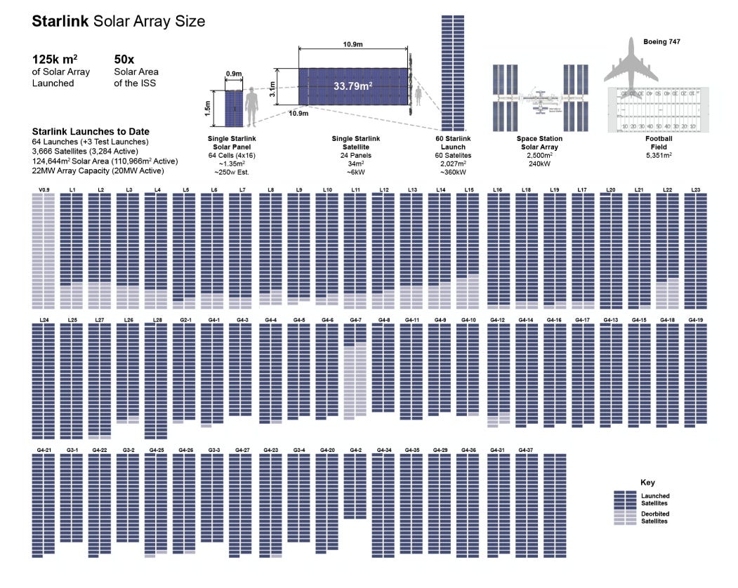
By contrast, solar energy is abundant, continuous, and scalable in orbit, making photovoltaic power generation the only solution that can support long-term, large-scale satellite deployment.

1月20日
Power Capability Defines Mission Capability and Lifetime
Solar panels and PV cells directly determine:
The satellite’s available on-orbit power budget
The upper limit of payload performance
The operational lifetime of the satellite
Even minor degradation in photovoltaic performance can be amplified at the system level, resulting in reduced payload capability, shorter mission duration, or complete mission failure. As a result, solar power systems are not merely supporting components—they are the foundation of satellite mission success.
Extreme Space Environments Create Unique Engineering Demands
Unlike terrestrial solar panels, satellite photovoltaic systems must operate under some of the harshest conditions known in engineering:
High-Radiation Exposure
Space is filled with high-energy particles such as cosmic rays, trapped radiation belts, and solar particles. These particles cause displacement damage and ionization effects in semiconductor materials, leading to gradual efficiency degradation. Space-grade solar cells must therefore exhibit exceptional radiation resistance and slow degradation rates to maintain output over years of operation.
AM0 Solar Spectrum and Intense UV Radiation
In space, solar radiation is not filtered by Earth’s atmosphere. Satellites are exposed to the AM0 solar spectrum, which contains significantly higher ultraviolet and high-energy components than terrestrial AM1.5 conditions. This environment accelerates material aging, oxidation, and interface degradation, requiring specialized cell structures, coatings, and encapsulation materials optimized for AM0 exposure.
Ultra-High Vacuum Conditions
In orbit, satellites operate in near-perfect vacuum. Many materials that perform well on Earth can suffer from outgassing, material embrittlement, or interface instability in vacuum. Solar cells and their encapsulation layers must demonstrate long-term vacuum stability and extremely low outgassing characteristics to ensure reliability.
Extreme and Rapid Thermal Cycling
Satellites experience repeated transitions between direct sunlight and Earth’s shadow, often every 45–90 minutes depending on orbit. Surface temperatures can swing from +100–130°C in sunlight to –150–200°C in shadow. Solar panels must withstand thousands of these cycles without cracking, delamination, electrical drift, or structural failure.
Reliability Is Not Optional—It Is Mission-Critical
Because satellites cannot be repaired once deployed, solar panels must operate reliably for years without failure. This drives stringent qualification standards, including radiation testing, thermal cycling, vacuum exposure, and long-duration reliability validation that far exceed terrestrial solar requirements.
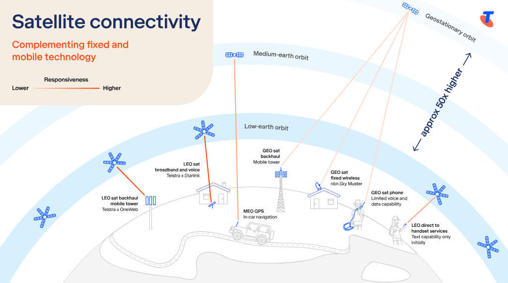
In large LEO constellations, where thousands of satellites are deployed simultaneously, power system reliability directly impacts:
Network uptime
Replacement cadence
Total cost of ownership
Overall constellation economics
Not a Choice, but a Necessity
For space satellites, solar power is not a matter of preference—it is a system-level inevitability. Solar panels define how much a satellite can do, how long it can operate, and whether its mission can succeed at all.
As satellite constellations grow larger and missions become more power-intensive—supporting broadband connectivity, edge computing, sensing, and AI processing—the performance, durability, and reliability of space-grade photovoltaic systems will become even more critical.
In space, power is destiny—and today, solar energy remains the only path forward.
GaAs-Based Space Solar Cells: Technology Status and Manufacturing Flow
Why GaAs Solar Cells Became the Mainstream Choice for Space

Gallium arsenide (GaAs)–based solar cells are currently the mainstream photovoltaic technology for space applications, especially in satellites and spacecraft. Unlike terrestrial solar cells, space solar cells must simultaneously satisfy extreme requirements: very high conversion efficiency, strong radiation resistance, high-temperature tolerance, and long operational lifetime.
GaAs belongs to the III–V compound semiconductor family, with a bandgap of approximately 1.42 eV, which matches the solar spectrum particularly well. Under the AM0 spectrum—the solar spectrum in space without atmospheric filtering—GaAs exhibits significantly higher photoelectric conversion potential than silicon. In addition, GaAs materials demonstrate superior radiation hardness and thermal stability, making them better suited for long-term orbital operation.
Since the 1990s, GaAs solar cells have gradually replaced silicon cells and become the core power-generation unit of spacecraft.
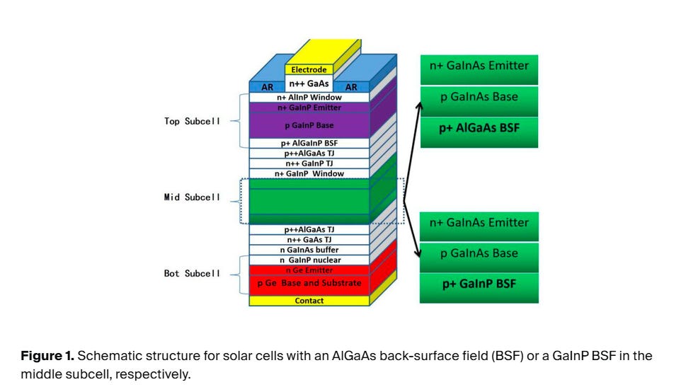
Improving Radiation Resistance of GaInP/GaInAs/Ge Triple-Junction Solar Cells Using GaInP Back-Surface Field in the Middle Subcell:The paper investigates how incorporating a GaInP back-surface field (BSF) in the middle subcell of GaInP/GaInAs/Ge triple-junction space solar cells affects their resistance to radiation. Compared with cells using an AlGaAs BSF, cells with a GaInP BSF demonstrate improved radiation tolerance under high-dose energetic electron irradiation. Although initial electrical performance is similar for both designs, the GaInP BSF structure degrades less in short-circuit current and overall efficiency after irradiation. The authors analyze the underlying mechanisms, attributing the enhanced radiation resistance to stronger electric fields and reduced interface state density at the heterojunction.
Triple-Junction GaAs: The Optimal Trade-Off Between Performance and Cost
GaAs space solar cells can be categorized into single-junction and multi-junction structures. Among them, triple-junction GaAs solar cells remain the dominant commercial solution today.
Multi-junction cells work by stacking semiconductor materials with different bandgaps, allowing each sub-cell to absorb a specific portion of the solar spectrum. This significantly improves energy utilization efficiency and power density. As technology evolves from triple-junction to four-junction or even five-junction designs, theoretical efficiency ceilings continue to rise.
However, higher junction counts come with:
Increased process complexity
Higher manufacturing costs
Tighter yield control requirements
When balancing efficiency, reliability, manufacturability, and cost, triple-junction GaAs solar cells currently offer the best overall equilibrium, making them the mainstream choice for space photovoltaic systems.
Manufacturing Flow of Triple-Junction GaAs Solar Cells
Taking triple-junction GaAs solar cells as an example, the manufacturing process can be broadly divided intosix major stages, each with highly specialized equipment and strict process control.
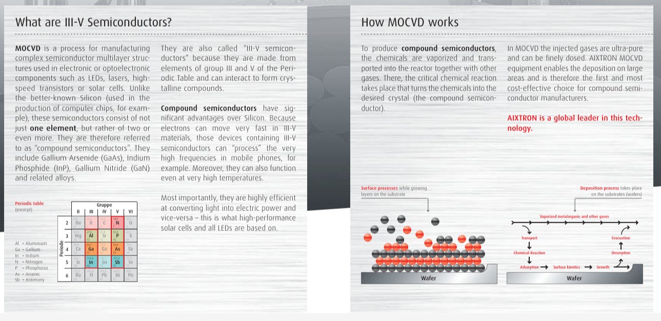
- Epitaxial Growth by MOCVD
The process begins with metal-organic chemical vapor deposition (MOCVD) on a GaAs substrate. Through sequential epitaxial growth, multiple sub-cells—typically GaInP (top cell), GaAs (middle cell), and Ge (bottom cell)—are formed.
Between adjacent sub-cells, highly doped p⁺/n⁺ tunnel junctions are grown to enable low-resistance series connection. Buffer layers, window layers, emitter regions, base layers, back surface fields, and tunnel junctions are all completed within a single MOCVD system, forming a complete inverted GaInP/GaAs/Ge triple-junction epitaxial structure.
Key equipment:MOCVD epitaxy systems
- Photolithography and First Etching (Cell Isolation)
Photolithography is used to define the active regions on the epitaxial wafer. After photoresist coating, exposure, and development, the exposed regions undergo first-stage etching, removing material down to the substrate.
This step simultaneously forms:
Electrical isolation trenches between cells
Dicing lanes for subsequent cell separation
The result is precise electrical isolation between individual solar cell units.
Key equipment:Photolithography tools and etching systems
- Ohmic Contact Patterning and Front Electrode Formation
Ohmic contact layers are formed on the cell surface, followed by photolithographic definition of electrode regions. Etching removes excess ohmic contact material, after which anti-reflection coatings (ARC) are deposited via evaporation or sputtering.
Subsequent photolithography defines front electrode openings, and etching removes ARC in those areas. Finally, front metal electrodes are deposited, ensuring reliable electrical contact while minimizing optical loss.
Key equipment:
Photolithography lines, metal deposition systems (evaporation/sputtering), thin-film deposition tools
- CIC Packaging and Interconnect Integration
After individual cells are fabricated, they undergo CIC packaging. Coverglass protects the cell from radiation and environmental damage, while interconnect structures enable series and parallel assembly.
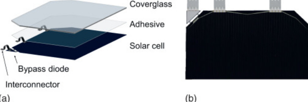
The goal is to integrate the solar cell, interconnects, and coverglass into a standardized module unit that can be directly assembled into a satellite solar array.
Key equipment:Coverglass bonding and interconnect welding systems
- Space Environment Simulation and Reliability Testing
Before launch, all space solar cells must pass rigorous ground-based space environment simulations, including:
High vacuum conditions
Solar radiation exposure
Thermal cycling
Cold darkness environments
These tests verify long-term reliability under orbital conditions where heat transfer is dominated by radiation and temperature extremes are severe.
Key equipment:Thermal vacuum chambers, electrical characterization tools, vibration and mechanical test systems
Cost Pressure in Large-Scale LEO Constellations
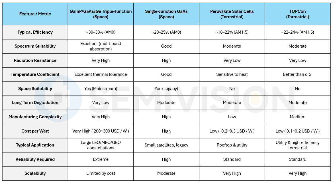
With the rise of satellite internet and large-scale LEO constellations, the high unit cost of GaAs solar cells has become increasingly visible.
Typical pricing:
GaAs-based triple-junction solar cells represent a mature, high-performance, and mission-proven solution for space power generation. Their dominance is rooted in unmatched efficiency under AM0 conditions, radiation resistance, and long-term reliability.
However, as satellite deployments shift from small batches to massive constellations, manufacturing complexity, yield control, and cost structure are becoming just as critical as efficiency. Future innovation in space photovoltaics will be shaped not only by physics limits—but by system economics and scalability.
In space, solar cells are not just components—they are strategic infrastructure.
Crystalline Silicon Solar Cells for Space: Manufacturing Flow and Material Choices
Manufacturing Flow of Crystalline Silicon Solar Cells
Compared with III–V multi-junction solar cells, crystalline silicon solar cells require a more complete upstream materials chain, starting from silicon crystal growth. The process begins with high-purity silicon feedstock and extends through wafering and cell fabrication, making the front-end supply chain more complex and capital-intensive.
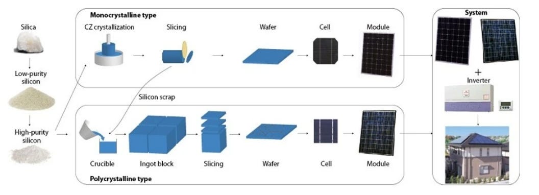
Source: Sharp
The manufacturing flow can be summarized in four main stages:
Silicon Preparation and Crystal Growth
Solar-grade silicon is first purified, crushed, and melted at high temperature. Through directional solidification or crystal pulling processes, monocrystalline or multicrystalline silicon ingots are formed. This step defines the crystal quality and defect density of the final wafers.
Ingot Slicing into Wafers
After cooling and shaping, silicon ingots are sliced into thin wafers using diamond wire saws. These wafers serve as the base material for subsequent solar cell processing and represent a major cost contributor in silicon photovoltaics.
Solar Cell Fabrication
Silicon wafers undergo cleaning, texturing, and surface treatment. Anti-reflection coatings and passivation layers are deposited, followed by the formation of front and rear electrode structures. These steps enable efficient collection and transport of photogenerated carriers.
Module Assembly and Encapsulation
Finished cells are electrically interconnected and encapsulated between glass and backsheet (or polymer layers) to enhance mechanical strength and environmental protection. Aluminum frames are typically added for structural reinforcement, resulting in complete solar modules ready for deployment.
Why Space Applications Prefer p-Type Solar Cells
In space environments, solar cells are continuously exposed to high-energy protons, electrons, and other energetic particles. These particles penetrate encapsulation layers and interact with the silicon lattice, causing atomic displacement damage, defect generation, and recombination center formation. Over time, this leads to irreversible performance degradation.
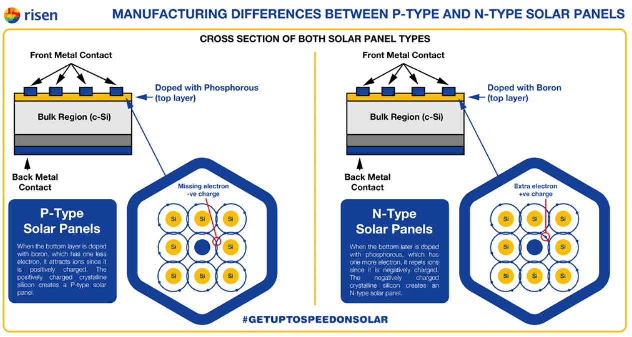
Under radiation-dominated degradation mechanisms, n-type silicon cells tend to degrade faster than p-type cells. In extreme radiation conditions, n-type cells may even experience so-called “type inversion,” where electrical characteristics become unstable or fail altogether. By contrast, p-type cells exhibit more stable and predictable degradation behavior, making them better suited for long-term orbital missions.
HJT Solar Cells: A Promising Successor to PERC Technology
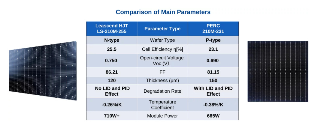
HJT stands for Heterojunction Solar Cell. As an n-type monocrystalline bifacial cell technology, HJT combines the advantages of crystalline silicon wafers with thin-film amorphous silicon layers. Thanks to its relatively simple process flow, high energy yield, and lower levelized cost of electricity (LCOE), HJT is widely regarded as a strong potential successor to today’s mainstream PERC solar cells.

Process Simplicity as a Core Advantage
One of the most significant advantages of HJT technology is its simplified manufacturing process. Unlike conventional crystalline silicon cells that rely on multiple high-temperature diffusion and annealing steps, HJT cells deposit hydrogenated amorphous silicon (a-Si:H) layers at low temperatures (~200 °C). This reduces process complexity, shortens cycle time, and lowers overall energy consumption during manufacturing.
High Efficiency and Bifacial Performance
Current HJT cells demonstrate front-side efficiencies of around 23%, with rear-side efficiency reaching up to 90% of the front-side output. This high bifaciality is mainly attributed to differences in shading area between the front and rear sides, which directly affect the short-circuit current (Isc). As a result, HJT modules can achieve higher real-world energy generation, especially in installations with high ground reflectivity.
Low-Temperature Interconnection Technology
Conventional crystalline silicon cells typically use infrared soldering at 200–240 °C, with solder ribbons composed of tin–lead–silver alloys. In contrast, HJT cells require low-temperature soldering, typically in the range of 150–190 °C. This has driven the adoption of new low-temperature ribbons, often based on tin–bismuth–silver or tin–bismuth alloys. By adjusting the bismuth content in the ribbon, manufacturers can precisely control soldering temperature while maintaining reliable electrical connections.
p-Type HJT Technology and Its Potential in Space
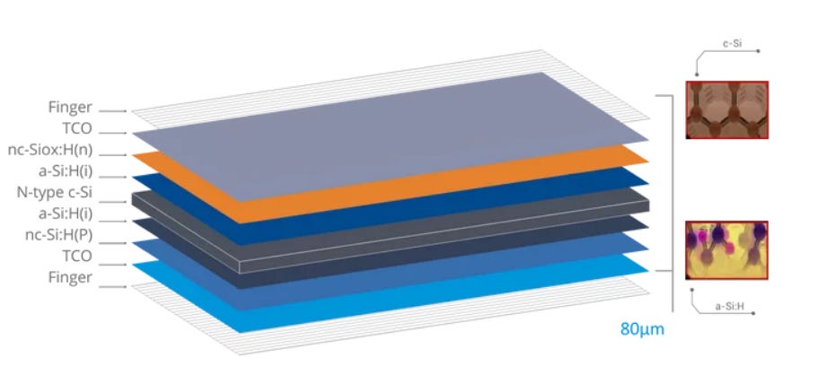
p-type heterojunction (HJT) solar cells use hydrogenated amorphous silicon (a-Si:H) as selective contact layers. In this structure:
n-type a-Si:H acts as the electron-selective contact (ESC)
p-type a-Si:H serves as the hole-selective contact (HSC)
Both are deposited on intrinsic a-Si:H passivation layers
This architecture provides excellent chemical passivation, effectively reducing open-circuit voltage (Voc) losses and improving carrier collection efficiency.
Potential Advantages of p-Type HJT in Space:
Radiation Tolerance and Partial Recovery
Experimental results, including those reported by the French National Institute for Solar Energy (INES), show that under AM0 illumination and 1 MeV electron irradiation, silicon heterojunction cells can maintain acceptable efficiency levels, demonstrating adaptability to space radiation environments.
Superior Temperature Coefficient
Studies on the temperature dependence of HJT solar cells indicate that p-type HJT cells can achieve a Pmax temperature coefficient as low as –0.20%/K across a wide temperature range (173–373 K). This is particularly advantageous for space applications, where solar arrays experience frequent and extreme thermal cycling.
Limitations and Trade-Offs
Crystalline silicon solar cells offer a well-understood, scalable manufacturing route and cost advantages derived from terrestrial photovoltaics. In space applications, p-type cells are favored over n-type due to superior radiation stability and thermal behavior, with p-type HJT emerging as a promising candidate for future low-Earth-orbit missions.
However, until further breakthroughs in radiation hardness and long-term reliability are achieved, III–V multi-junction solar cells will remain the dominant solution for high-performance space power systems, while silicon technologies continue to explore niche and cost-sensitive applications in orbit.
Third-Generation Photovoltaics: Perovskite Solar Cells and Tandem Architectures
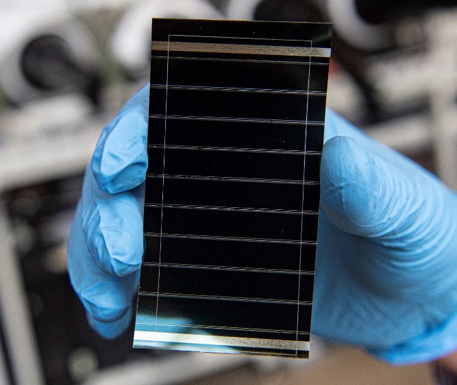
Source: National Renewable Energy Laboratory
Perovskite Solar Cells as a New Photovoltaic Platform

Perovskite solar cells are a new class of photovoltaic devices that use organic–inorganic metal halide semiconductors with a perovskite crystal structure as the light-absorbing layer. The term “perovskite” broadly refers to materials with an ABX₃ crystal structure, where the A, B, and X sites can be flexibly substituted. This compositional freedom enables continuous tuning of electronic and optical properties through material design.
Because of this high degree of tunability, perovskite solar cells are widely regarded as one of the most promising and disruptive third-generation photovoltaic technologies.
The Evolution of Perovskite Solar Cells: From Laboratory Curiosity to Commercial Contender
The development of perovskite solar cells has been one of the most remarkable stories in modern photovoltaic research, marked by rapid efficiency gains and expanding application potential.
Before 2005, perovskite materials were primarily investigated for non-solar applications, such as light-emitting devices and other optoelectronic uses. Their unique crystal structure and tunable properties attracted academic interest, but their photovoltaic potential had not yet been fully recognized.
A major turning point came in 2009, when the first perovskite solar cell was demonstrated. Although its efficiency was modest, this milestone proved that perovskite materials could function as effective light absorbers in solar cells, opening an entirely new research direction.
By 2013, progress accelerated dramatically. The first perovskite solar cells surpassed 10% power conversion efficiency, a threshold that typically takes decades for new photovoltaic technologies to reach. This rapid improvement captured global attention and positioned perovskites as a serious alternative to conventional photovoltaic materials.
In 2014, researchers achieved another breakthrough with the demonstration of the first perovskite–silicon tandem solar cell. By stacking a perovskite top cell on a crystalline silicon bottom cell, this architecture showcased the ability of perovskites to complement existing silicon technology and break through the efficiency limits of single-junction devices.
By 2024, record perovskite-based solar cells achieved efficiencies exceeding 26%, bringing the technology firmly into the range required for commercialization discussions. Research efforts have increasingly shifted from purely efficiency-driven goals toward stability, scalability, and manufacturing readiness, signaling a transition from laboratory innovation to industrial relevance.
Overall, the evolution of perovskite solar cells illustrates how a materials platform can move from niche research to a leading candidate for next-generation photovoltaics in little more than a decade—reshaping expectations for both efficiency improvement and technology development cycles in the solar industry.

Core Advantages of Perovskite Photovoltaics
- Tunable Bandgap and High Theoretical Efficiency
Perovskite materials are artificially designed systems whose bandgaps can be continuously adjusted by modifying composition. This allows perovskite cells to operate either as standalone single-junction devices or as top cells in tandem structures with crystalline silicon or other absorbers.
By stacking materials with different bandgaps, tandem solar cells can absorb a broader portion of the solar spectrum, overcoming the efficiency limits of single-junction devices. The theoretical efficiency limit of single-junction perovskite cells is around 31%, while perovskite–silicon tandem cells are projected to exceed 43% in theory.
- Simplified Manufacturing and Lower Capital Intensity
Compared with crystalline silicon solar cells, perovskite devices offer a significantly simplified manufacturing flow. They require lower processing temperatures, fewer high-cost steps, and reduced upfront capital expenditure. This makes perovskites particularly attractive for cost-sensitive, high-efficiency photovoltaic applications.
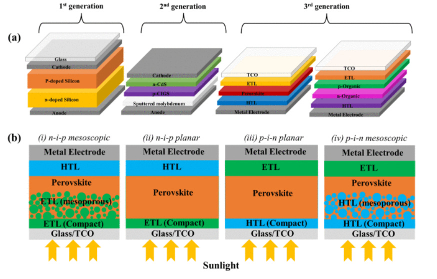
Device Categories: Single-Junction and Tandem Perovskite Cells
Currently, perovskite photovoltaics are primarily divided into:
Single-junction perovskite solar cells
Tandem perovskite solar cells
Single-junction perovskite cells can be further classified into n–i–p and p–i–n architectures, depending on the stacking order of the electron transport layer, perovskite absorber, and hole transport layer.
Tandem perovskite cells mainly follow two technological routes:
Perovskite–silicon tandems
All-perovskite tandems
Thanks to their adjustable bandgaps, perovskite materials are particularly well suited for multi-junction designs, enabling broader spectral coverage and higher conversion efficiency.
Efficiency, Complexity, and Cost: 2T, 3T, and 4T Tandem Architectures
Perovskite–silicon tandem solar cells can be classified into two-terminal (2T), three-terminal (3T), and four-terminal (4T) architectures, based on electrical interconnection and carrier extraction methods. This classification directly determines electrical coupling, current-matching requirements, device complexity, and system integration cost.
Four-Terminal (4T) Tandem Architecture
In a 4T tandem structure, the perovskite top cell and silicon bottom cell are fabricated independently and then mechanically stacked. Each sub-cell has its own pair of electrodes, resulting in four terminals in total.
Key characteristics:
Independent electrical extraction from top and bottom cells
Each sub-cell can operate at its maximum power point
Minimal current-matching constraints
From a system perspective, the independent outputs may require separate power electronics or inverters, increasing system-level complexity. However, since the top perovskite cell typically contributes roughly one-third of total power, inverter sizing can be optimized accordingly.
Two-Terminal (2T) Tandem Architecture
In a 2T tandem structure, the perovskite top cell is deposited directly onto the silicon bottom cell, and the two sub-cells are electrically connected in series. Only one transparent electrode is required.
Key characteristics:
Simplified device structure and lower manufacturing cost
Strong electrical coupling between sub-cells
Strict current-matching requirements
In this configuration, carriers generated in the perovskite top cell must be efficiently transferred into the silicon bottom cell. This places stringent demands on interface quality, optical transparency, and electrical coupling. Despite these challenges, 2T architectures are attractive for large-scale manufacturing due to their compact structure and cost advantages.
Three-Terminal (3T) Tandem Architecture
The 3T tandem structure introduces a third electrical terminal, creating a hybrid configuration between 2T and 4T designs. In this architecture, the top and bottom cells are neither fully series-connected nor fully independent.
Key characteristics:
Three electrodes: one on the front side and two on the rear side
Relaxed current-matching constraints compared with 2T
Potentially higher efficiency than 2T designs
Although 3T tandems are still relatively less explored, they offer significant efficiency potential by balancing electrical decoupling with reduced system complexity.
Perovskite solar cells represent a transformative step toward high-efficiency, low-cost photovoltaic systems, driven by bandgap tunability and simplified manufacturing. When combined with silicon in tandem architectures, perovskites open a clear pathway beyond the efficiency limits of conventional single-junction cells.
The choice among 2T, 3T, and 4T tandem architectures reflects a fundamental trade-off between efficiency, device complexity, and system cost. While 4T designs offer maximum flexibility and performance, 2T structures promise scalability and cost efficiency, and 3T architectures may ultimately provide the optimal balance between the two.
As materials stability, interface engineering, and large-area manufacturing continue to improve, perovskite-based tandem photovoltaics are poised to play a central role in the next generation of solar energy technology.
From Interfaces to Series Connection: Structural Advantages of HJT–Perovskite Tandem Solar Cells
Why Choose HJT–Perovskite Tandem Solar Cells?
Heterojunction (HJT) silicon solar cells offer structural and process advantages that make them particularly well suited for integration with perovskite top cells in tandem architectures.
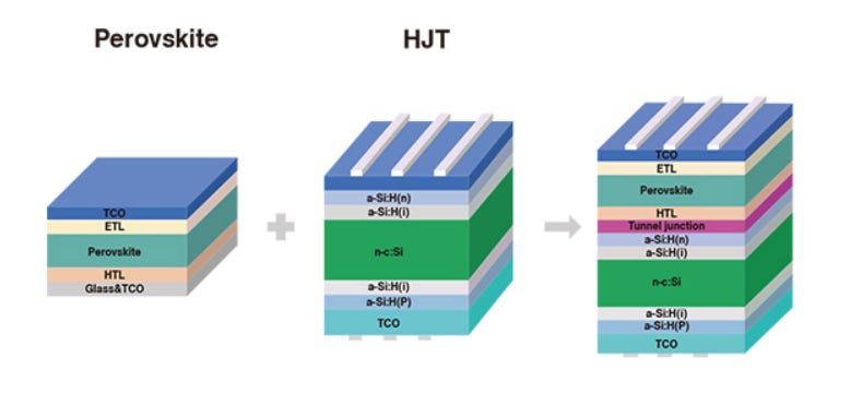
- HJT Cells Are Structurally More Compatible with Perovskite Tandems
When perovskite layers are stacked on heterojunction silicon cells, the surface of the HJT cell already consists of a transparent conductive oxide (TCO) layer, which can directly function as the bottom electrode of the perovskite sub-cell. As a result, existing HJT production lines require minimal modification to accommodate perovskite stacking.
This inherent structural compatibility significantly lowers integration complexity compared with other silicon technologies.
- Series-Connected HJT–Perovskite Tandems Enable Ultra-High Output Voltage
HJT–perovskite tandem solar cells typically adopt a series-connected (2T) architecture, leveraging the strong spectral and electrical matching between perovskite absorbers and heterojunction silicon cells. This configuration enables power conversion efficiencies that exceed those of single-junction perovskite devices.
In HJT cells, crystalline silicon is combined with amorphous silicon layers on the same wafer, forming high-quality PN junctions at the interface. The amorphous silicon layers effectively passivate interface defects, thereby increasing open-circuit voltage (Voc) and overall conversion efficiency.
In a typical tandem design:
The perovskite top cell primarily absorbs short- and mid-wavelength light.
The HJT silicon bottom cell absorbs longer-wavelength light transmitted through the perovskite layer.
Through coordinated optical and electrical design, the two sub-cells operate in series to deliver ultra-high combined voltage output. Under standard conditions, heterojunction silicon cells contribute approximately 25–26% efficiency, while the perovskite top cell can further increase total efficiency by 3–5 percentage points.
Because both perovskite and silicon sub-cells share a PN-junction-based transport mechanism, direct PN-junction contact at the interface must be avoided, as it would lead to carrier recombination and electrical blocking. Therefore, an intermediate transport layer is required to provide:
Good electrical conductivity
High optical transparency
Appropriate thickness
This ensures efficient charge transfer between the two sub-cells.
- Low-Temperature Metallization Compatibility
HJT technology relies on low-temperature metallization pastes and low-temperature curing processes, which are fully compatible with the metal electrode formation required after perovskite stacking. This low-thermal-budget process flow is essential for preserving the integrity of temperature-sensitive perovskite materials.
By combining structural compatibility, excellent interface passivation, strong spectral matching, and low-temperature processing, HJT silicon cells provide an ideal foundation for high-efficiency perovskite tandem architectures. These advantages make HJT–perovskite tandems one of the most promising pathways toward next-generation ultra-high-efficiency photovoltaic technologies.
From Mass-Production Feasibility to Long-Term Reliability: A Comparison of Photovoltaic Technologies
From the perspective of current technology maturity and overall performance, p-type HJT solar cells represent one of the most well-rounded technology pathways within crystalline silicon photovoltaics today. They have already achieved large-scale mass production and demonstrate balanced performance across multiple critical dimensions, including particle radiation resistance, thin-wafer potential, controllable material costs, cell efficiency and long-term reliability, as well as manageable patent risk.
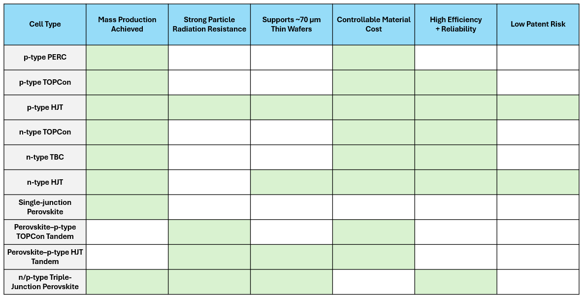
Building on this foundation, p-type HJT–perovskite tandem solar cells inherit the structural and process advantages of p-type HJT while introducing a perovskite top cell to further push the efficiency frontier. At the same time, they maintain strong fundamentals in radiation tolerance, thin-wafer compatibility, and material cost controllability. Through the combination of a mature bottom cell platform and a high-efficiency top cell, p-type HJT–perovskite tandems have the potential to emerge as a technology choice that balances performance potential with engineering feasibility over the long term.
In this article, we explored the arrival of the mega-constellation era and asked a fundamental question: who will provide continuous power for satellites in orbit? By examining the unique requirements of space environments, we walked through the evolving role of solar panels as the backbone of satellite power systems, from technology choices to long-term reliability and scalability. As satellite numbers grow rapidly and missions become more power-intensive, the demand for high-efficiency, radiation-tolerant, and cost-effective space photovoltaics will only intensify. Understanding these trends is essential to understanding the future of the space economy itself.

Recently, Tesla and SpaceX have dispatched technical and strategic teams to conduct on-site visits across the Asian solar supply chain, with evaluations spanning equipment manufacturing, silicon wafers, solar cell modules, and next-generation technology pathways such as perovskites.
Compared with traditional crystalline silicon solar cells, perovskite-based technologies exhibit several structural advantages:
Conventional silicon solar cells have reached a mature efficiency level, but their manufacturing processes are energy-intensive, with high material and equipment costs.
Perovskite solar cells can be fabricated as ultra-thin, and even flexible, thin-film structures, significantly reducing material consumption.
Perovskites can be integrated with silicon cells in tandem architectures, offering a pathway to surpass the efficiency limits of single-material devices.
Under laboratory conditions, the power conversion efficiencies of perovskite cells and perovskite-based tandem structures have already approached—and in some cases exceeded—those of mainstream commercial technologies. As a result, perovskites are widely regarded as a key candidate for the “post-silicon era” of photovoltaics.
Following media coverage of these visits, the market reacted swiftly:
Leading Chinese solar companies, including JinkoSolar, Trina Solar, and TCL Zhonghuan, saw their share prices strengthen.
Companies involved in perovskite and heterojunction (HJT) technologies attracted heightened attention from capital markets.
This response underscores a key reality: even before any concrete investment decisions are made, Elon Musk’s technological direction alone has become a powerful market catalyst.

Source: NASA
Overall, the space photovoltaic sector faces multiple layers of uncertainty despite its strong long-term potential. Key risks include technology maturity and long-term reliability, as many solutions remain in the R&D and engineering validation stage and lack extensive in-orbit data. Industrialization and commercialization challenges persist due to high customization, long verification cycles, and the absence of standardized delivery models. In addition, early-stage investment and execution risks are elevated given long development timelines, high capital intensity, and sensitivity to technical and program delays. The industry is also exposed to market and competitive uncertainties, as alternative technologies or faster-moving competitors could reshape the landscape. Finally, policy and regulatory changes in launch, spectrum, and space governance may significantly influence technology adoption paths and long-term industry development.

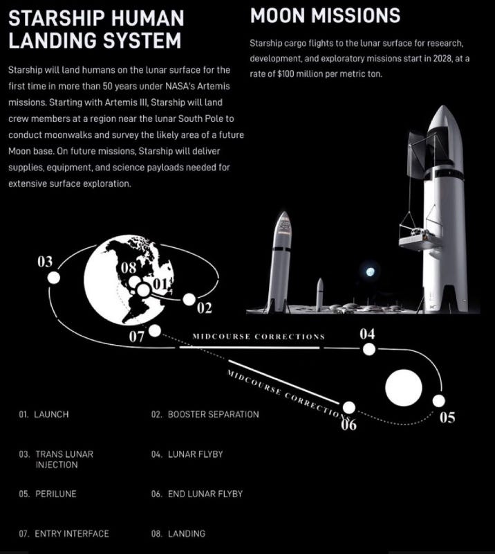
Elon Musk announced on X that SpaceX has shifted its focus toward building a self-sustaining city on the Moon. Lunar travel may be closer than we think
According to Musk, a lunar city could become reality within 10 years, while Mars would require at least 20 years. Missions to the Moon could launch every 10 days, with a travel time of just two days. Compared with Mars, the Moon’s proximity enables far faster construction, iteration, and scaling—making it the most practical next step toward humanity’s off-world future.


PreviousNext
TopLatestDiscussions








See all