Can ZAM Replace HBM? Intel and SoftBank Push Radical Memory Architecture
Can ZAM Replace HBM? Intel and SoftBank Push Radical Memory Architecture
- Source: SemiVision
- Author: SEMIVISION
- Published: 2026-02-05T10:07:40+08:00
- URL: https://tspasemiconductor.substack.com/p/can-zam-replace-hbm-intel-and-softbank Can ZAM Replace HBM? Intel and SoftBank Push Radical Memory Architecture


Can ZAM Replace HBM? Intel and SoftBank Push Radical Memory Architecture
Original Article By SemiVision Research (Intel, Softbank, SaiMemory, PSMC)

Feb 05, 2026
∙ Paid

As the global AI compute race accelerates, the real bottleneck is no longer GPU architecture, but the physical limits of memory. HBM capacity remains tightly controlled by Samsung Electronics, SK hynix and Micron. Tight supply, strong pricing power, and slow expansion cycles have led to a recurring structural imbalance across the AI supply chain from 2024 to 2026: “compute available, memory constrained.”This is not a short-term cyclical issue, but a structural lock-in caused by a single dominant technology path—once high-bandwidth memory became synonymous with HBM, supply chain control naturally concentrated.
It is precisely within this highly concentrated yet structurally fragile landscape that theSaiMemory (ZAM, Z-Angle Memory)initiative, driven byIntelandSoftBank, gains strategic significance. This is not merely another DRAM specification company; it is better understood as an AI-era memory architecture venture platform. Its formation stems from the convergence of three forces:

The real driver behind ZAM’s formation: supply-chain risk management, not just technology advancement
ZAM did not originate from “we have a better memory,” but from a more urgent realization:
“AI infrastructure cannot remain dependent on only two Korean memory vendors.”
For Intel, this is fundamentally a platform control issue. If future AI servers remain locked into GPU + HBM architectures, then:
Memory supply cadence ≈ Korean vendors’ capex cycles
Platform innovation speed ≈ HBM TSV process evolution
That effectively places the tempo of AI computing under external control—strategically unacceptable for Intel as it rebuilds its advanced process and data center ecosystem.
For SoftBank, this is a matter of investment structure risk. AI investment has shifted from software models toward infrastructure. If the compute foundation is constrained by HBM:
AI ROI timelines become tied to memory industry cycles
Rack density and power economics become unpredictable
ZAM thus functions as a form of infrastructure hedging—its very existence is meant to break single-path dependence on HBM.
SAIMEMORYis a subsidiary established by SoftBank in December 2024 to promote research and development of next-generation memory technologies.
SAIMEMORY aims to launch prototype products by fiscal year 2027 and achieve commercialization by fiscal year 2029. Through ZAM technology, the two companies will work to enable large-capacity, high-bandwidth data processing in data centers that require large-scale AI model training and inference, while improving processing performance and reducing power consumption.
According to a report by Nikkei, SAIMEMORY and Intel aim to cut power consumption by half compared to current products. SAIMEMORY President Hideya Yamaguchi stated at a technology event held in Tokyo on the 3rd that the initiative will address issues related to heat dissipation, performance, and supply, describing it as “a disruptive challenge in a sense.” Joshua Fryman of Intel, who is involved in the development, noted that the project could lead to the development of memory that is cheaper than HBM.

Sandia National Laboratories
Intel has long collaborated with Sandia National Laboratories on the Next-Generation DRAM Bonding (NGDB) technology. According to official statements, traditional HBM solutions often require trade-offs between bandwidth and capacity, whereas NGDB is designed to eliminate this constraint. The technology aims to bridge the performance gap between HBM and conventional DDR DRAM while delivering higher energy efficiency.
Intel emphasizes that NGDB demonstrates an innovative memory architecture combined with a revolutionary assembly process. It can significantly optimize DRAM performance and cost, and is expected to create transformative opportunities for low-power memory solutions.
ZAM’s corporate positioning: less a memory vendor, more an architecture integrator
Traditional memory companies follow this logic:
Design DRAM → expand fabs → compete on cost per bit
ZAM resembles a “memory architecture IP company + 3D manufacturing coordination platform.” It defines a non-TSV high-bandwidth memory path through:
Architectural patents
3D stacking physical design
Co-development of process windows with foundries
This explains why ZAM must exist as an independent entity—if it were tied to an incumbent memory maker, its roadmap would immediately conflict with HBM’s entrenched interests.
ZAM is not “next-generation HBM,” but a de-HBM path.
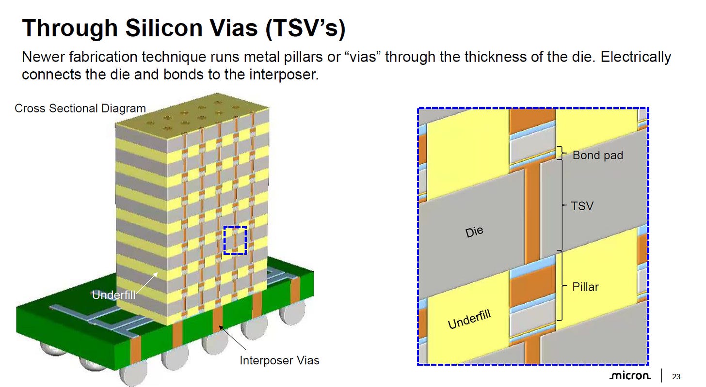
The essence of HBM is stacking multiple DRAM dies vertically using TSVs (Through-Silicon Vias), then connecting them to logic through an interposer. By the time the roadmap reaches HBM4, this path is approaching three fundamental limits:
Physical Challenges Faced by HBM
Structural Limit:
HBM stacks rely on thousands of TSVs (Through-Silicon Vias) per die. These vertical interconnects consume valuable silicon area that could otherwise store data, reducing effective memory density. High TSV density also weakens wafer mechanical integrity, increasing warpage risk, stress concentration, and die cracking during thinning and stacking. Yield sensitivity rises sharply as stack height increases.
Thermal Limit:
As stack layers increase (12-Hi, 16-Hi and beyond), middle dies become thermal dead zones. Heat generated by logic and active DRAM cells must pass through multiple low-conductivity layers before escaping, creating thermal gradients, hot spots, and retention degradation. Cooling efficiency drops non-linearly with height, forcing lower operating frequency or aggressive thermal throttling.
Power Limit:
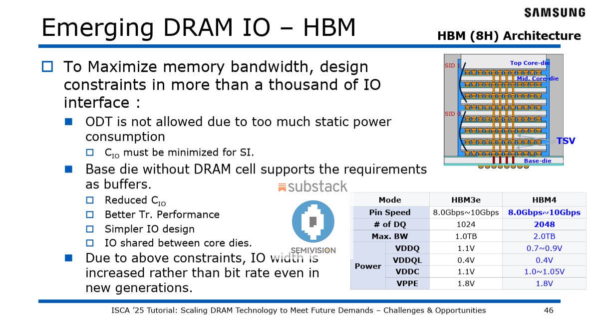
Signals must traverse microbumps, redistribution layers, and TSV channels, each adding resistance, capacitance, and inductive parasitics. This multi-interface path increases I/O power, reduces signal integrity, and raises energy per bit transferred. As bandwidth scales upward, I/O power becomes a dominant portion of total memory power, reducing system-level energy efficiency.

2025年10月13日
The core idea behind ZAM is simple:
Stop drilling everywhere. Build one central trunk instead.
“Via-in-One” Central Channel: A Structural Dimensional Shift
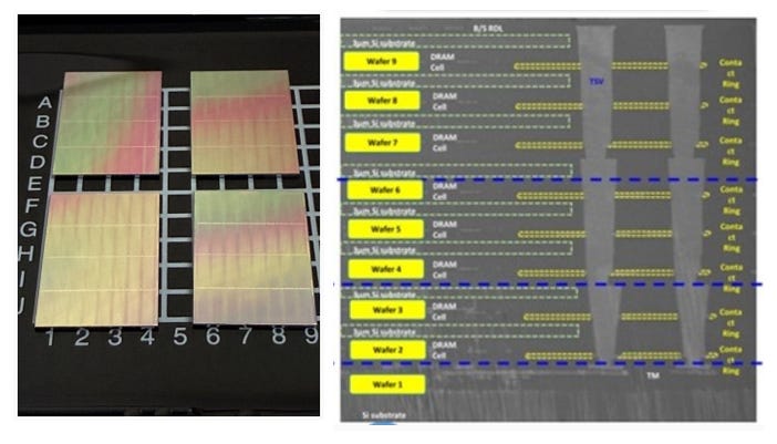
NOVEL ARCHITECTURE – The cross-section of an NGDB test assembly above illustrates the unconventional assembly. Eight wafers containing the novel NGDB DRAM architecture are vertically bonded on a base wafer and connected using an alternative “via-in-one” construct. (Photo provided by Intel)
ZAM uses a single central channel to deliver power and signals, replacing HBM’s “honeycomb TSV mesh” with a single-axis neural trunk.
What does this achieve?
Effective DRAM storage area increases by 30%+
Shorter signal paths → lower latency
Stronger mechanical integrity → wafers tolerate higher stack heights
This is not process optimization — it is a rewrite of memory architecture physics.
Native Heat-Pipe Effect: Turning Cooling into a Structural Advantage
HBM follows the rule: the higher the stack, the hotter the core.
ZAM’s central channel acts like a vertical heat pipe, allowing core heat to be conducted out more directly. Experimental data suggests that under equivalent compute workloads, ZAM power consumption could be around 50% of HBM4.
For AI data centers, this is not incremental — it is a rack-density–level revolution
Bumpless Bonding: Electrons No Longer “Climb Mountains”
ZAM relies on direct silicon-to-silicon hybrid bonding, not microbumps.
Signals no longer pass through solder joints, oxide interfaces, or discontinuous material boundaries. Instead, they move across near atomic-level contact, dramatically reducing resistance and parasitic inductance.

2025年7月13日

2025年7月11日
Intel Patent: Package architectures having vertically stacked dies for high capacity memory

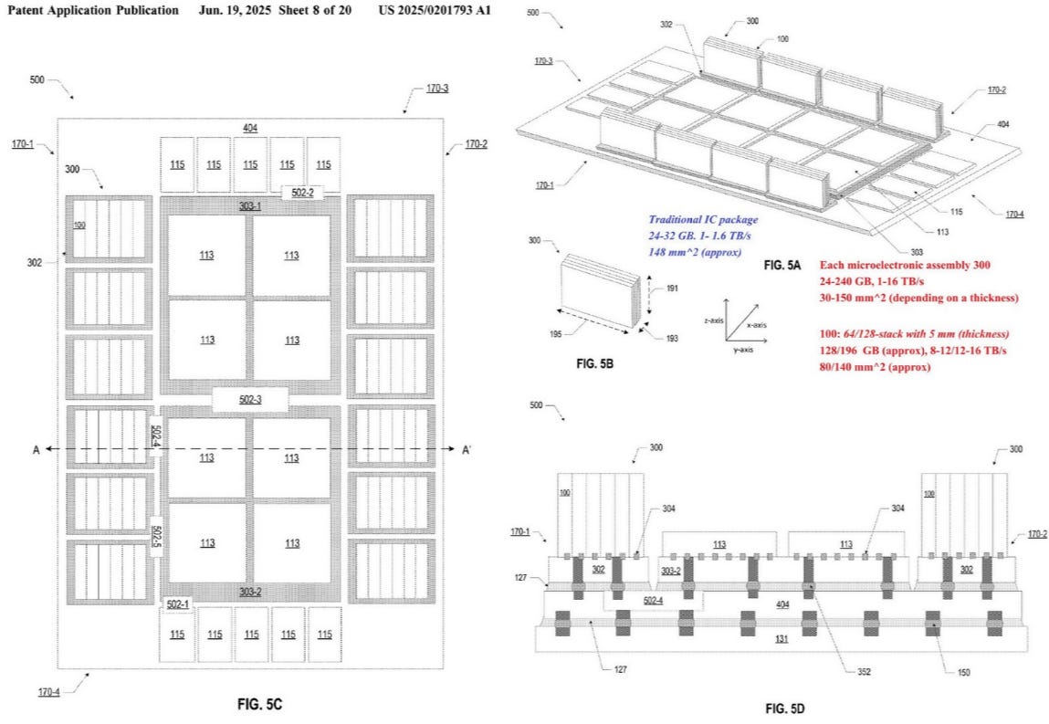
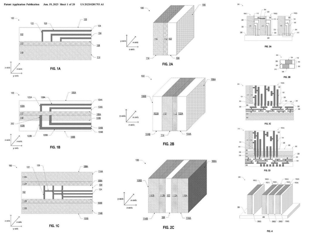
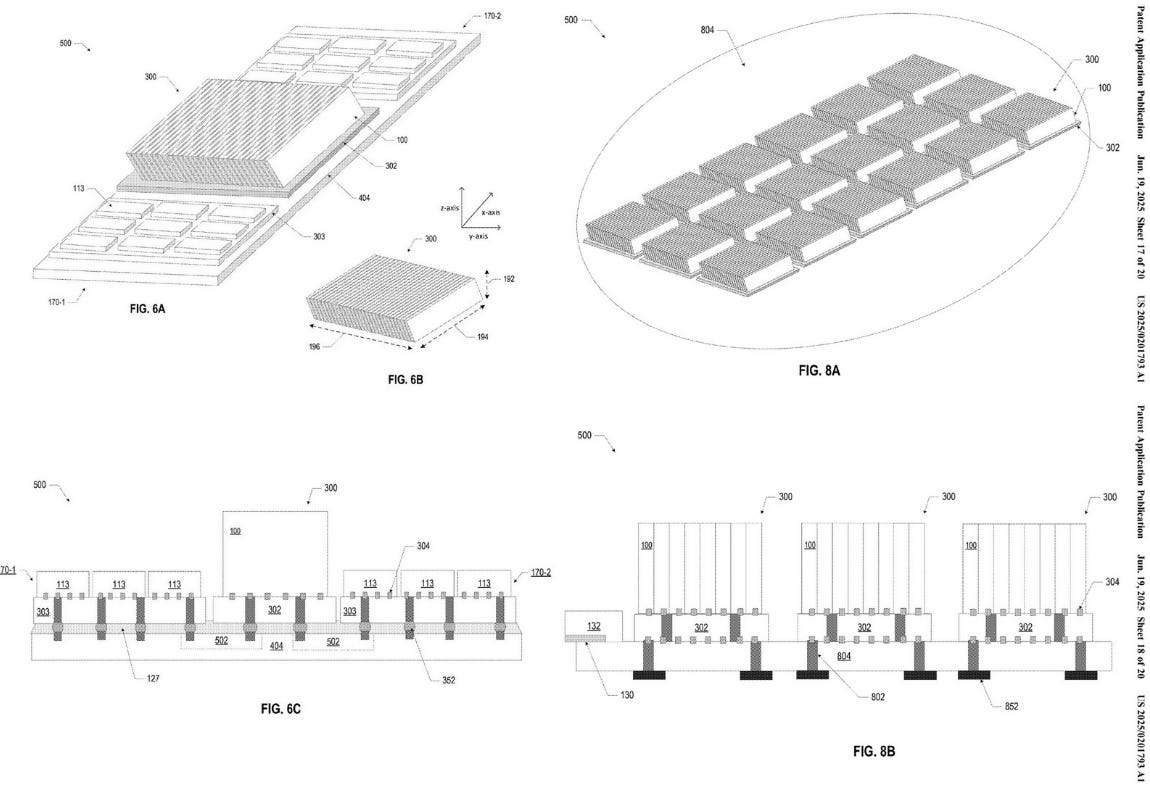
Intel’s recently published US patent— “Package architectures having vertically stacked dies for high capacity memory”describes a packaging structure that departs from the classic HBM model in several crucial ways. Rather than simply stacking DRAM dies vertically and placing them beside a logic die on an interposer, the patent outlines a multi-assembly, system-scale memory architecture where memory capacity and bandwidth are scaled through modular vertical stacks integrated at the package level.
This is not a minor packaging tweak. It represents a shift in how memory density is physically achieved.
For Paid member:
Why not TSMC, not Samsung Electronics — but Powerchip Semiconductor Manufacturing Corp. (PSMC)?
3 Moat of PSMC in Zam Technology
Inside PSMC: The Foundry Bridging Memory, Logic, and Advanced 3D Stacking
PSMC Open Foundry Platform
PSMC Market and Product Development Updates
PSMC Operational Strategy and Future Development
Traditional HBM vs. the Patent’s Approach
In a conventional HBM package:
Memory dies are stacked in a single column
TSVs provide vertical interconnect
The stack is coupled laterally to a logic die via an interposer
Capacity is limited by:
Stack height (thermal + yield limits)
Interposer real estate
Packaging complexity
The patent describes something fundamentally different:
Multiple “microelectronic assemblies” (memory stacks) can be arranged across the package substrate, not just a single HBM column.
Each assembly may contain 64-stack or even 128-stack memory die structures, with reported capacities of:
24–240 GB per assembly
Bandwidth in the range of 1–16 TB/s
Footprints as small as 30–150 mm² per module
This modular approach changes the scaling axis from:
“How tall can one stack be?”
“How many high-density stacks can be tiled across the system?”
That is a system architecture change, not just a memory improvement.
Why This Matters for ZAM
ZAM’s core philosophy is to break free from the TSV-bound, monolithic HBM paradigm. This patent aligns with that trajectory in three important ways:
1.Decoupling Capacity from a Single Stack
Instead of pushing one stack to extreme height (which creates thermal and yield challenges), memory density is distributed across multiple vertically integrated assemblies. This resembles ZAM’s goal of escaping HBM’s geometric limits.
2.Memory as Modular Infrastructure
The patent frames memory as repeatable, tileable modules rather than a single package-bound block. This mirrors the ZAM philosophy of treating memory as infrastructure units, not just on-die extensions.
3.System-Level Bandwidth Scaling
By using multiple high-bandwidth assemblies rather than one massive stack, total system bandwidth scales horizontally. This is conceptually closer tomemory fabricsthan to traditional “HBM next to logic” thinking.
ZAM challenges HBM at the memory architecture level.
This Intel patent shows that the industry is already experimenting with packaging structures that:
Treat memory as multiple scalable vertical modules
Push density beyond conventional HBM stacks
Decouple system capacity growth from TSV tower limits
In other words:
ZAM may be thearchitecture vision,
and patents like this reveal thepackaging paththat could make that vision real.
The post-HBM world is not built by one breakthrough — it emerges from the convergence of:
New memory architectures (like ZAM)
Advanced 3D stacking techniques
Modular, tileable package designs
This patent suggests that the industry is quietly preparing the physical foundation for that transition.
Why not TSMC, not Samsung Electronics — but Powerchip Semiconductor Manufacturing Corp. (PSMC)?
The biggest barrier for ZAM is not design. It is this:
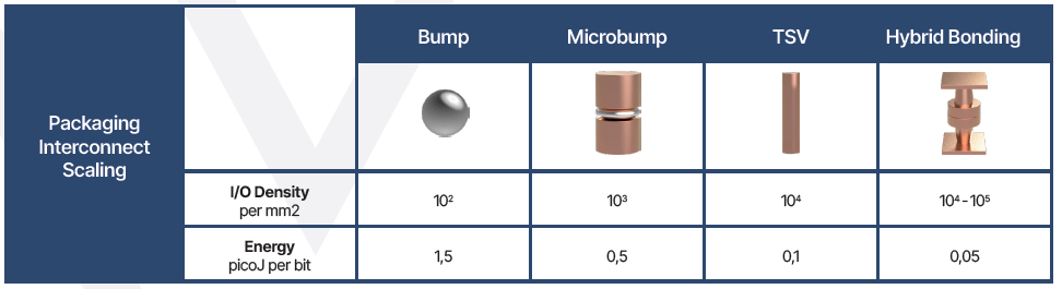
Mass production of atomic-level Wafer-on-Wafer (WoW) hybrid bonding between a full logic wafer and a full DRAM wafer.
This is not packaging. It is a front-end–class stacking engineering problem.
Moat #1: Rare global experience in WoW mass production

Most foundries excel atdie-to-dieorchiplet-basedintegration.
ZAM, however, requires:
Full 300 mm wafer-to-wafer alignment and bonding
This technology demands:
Alignment error controlled at nanometer scale
Simultaneous control of surface planarity, copper pad height, oxide thickness, and contamination
Any local defect → entire wafer scrap
Unlike chiplet packaging, yield here is multiplicative across the full wafer area, making process stability exponentially harder.
PSMC has spent years building WoW capability at its Tongluo fab. This is not something that can be quickly replicated through capital alone; it is the result of long-termprocess integration learning curves, defect density reduction, and CMP/bonding co-optimization.

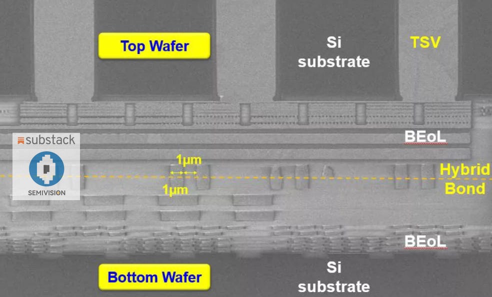
Source: PSMC
Without such a production line, ZAM would remain an academic architecture, not a manufacturable product.
Moat #2: A neutral “Open Foundry” position
If Intel worked with Samsung:
It would be handing core memory architecture to a primary HBM incumbent.
If Intel relied on TSMC:
Advanced packaging capacity (e.g., CoWoS) is already heavily allocated to GPU customers
Cost structures are optimized for leading-edge logic, not memory-centric 3D stacks
PSMC’s advantages:
No in-house branded memory products
No competition with customers’ end markets
Willingness to customize process windows for partner architectures
This neutrality allows Intel to share deep 18A logic-layer parameters for co-optimization without fear of ecosystem conflicts.

2025年5月1日
Moat #3: A cost structure purpose-built for 3D AI integration
HBM’s cost challenge is not just the die — it is:
Yield × stacking complexity × TSV overhead
TSV formation, wafer thinning, microbump bonding, and stack testing each introduce compounded yield loss.

PSMC’s transition toward a 3D AI Foundry model means its fabs are architected around:
Heterogeneous integration (memory + logic)
Wafer-level stacking flows
Process steps optimized for bonding yield rather than extreme node scaling
In this structure, the factory exists for stacking, not as an extension of a logic-only roadmap.
Under a mature WoW flow, ZAM could potentially achieve 20%+ lower cost than HBM, driven by:
Higher effective silicon utilization (no TSV arrays)
Fewer interconnect interfaces
Reduced packaging complexity
TSMC dominates advanced logic.
Samsung dominates memory manufacturing.
But ZAM sits in the narrow intersection of memory architecture innovation + wafer-level 3D stacking manufacturing + ecosystem neutrality.
That intersection is where PSMC becomes uniquely positioned.
The True Nature of the Z Program: A Redistribution of Supply Chain Power
On the surface, the Z Program appears to be a contest over memory technology. But from an industry power-structure perspective, it is fundamentally an effort to reallocate control within the supply chain. The core shift is not about improving a single component’s performance, but about who defines the memory architecture standards that AI compute depends on.
Over the past decade, the rise of HBM has made high-bandwidth memory almost synonymous with the Korean supply chain. Once a technology path becomes tightly bound to specific processes (TSV) and specific vendors, the entire AI hardware ecosystem becomes implicitly locked into that trajectory. The significance of the Z Program lies in breaking this single-path dependency, where technology equals power and process equals control.
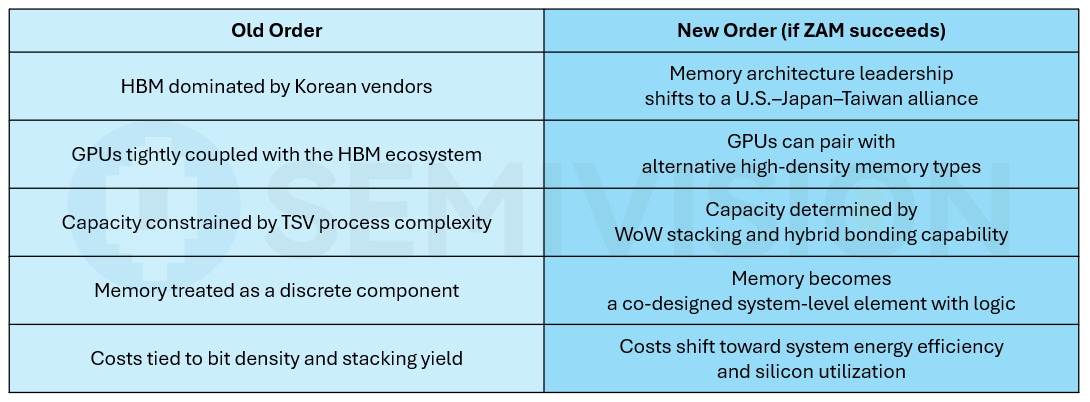
This signals a deeper transformation:
Memory is evolving from a “capacity product” into a structural part of system architecture.
In this new order, competition is no longer about who can produce the most gigabits, but about who can deliver the bestcompute density × energy efficiency × thermal structureas an integrated solution. The boundary between memory and logic begins to blur, and supply chain value shifts from component manufacturing to cross-layer integration capability.
It is within this redistribution of power that Powerchip Semiconductor Manufacturing Corp. (PSMC) is redefined.
PSMC is no longer merely “a smaller TSMC,” but a manufacturing hub positioned at the entry point of next-generation memory architecture. As the key bottleneck in memory evolution shifts from TSV to WoW hybrid bonding, fabs that master this capability effectively hold the production gate of the new memory era.
PSMC’s role thus evolves from a traditional foundry into:
A core manufacturing node for the “arms supply” of AI memory infrastructure.
Why This Company Had to Be Multinational by Design
ZAM was never conceived as a single-nation initiative. From the outset, it functioned as a technology-neutral alliance structure, purpose-built to separate architectural innovation from entrenched manufacturing interests.
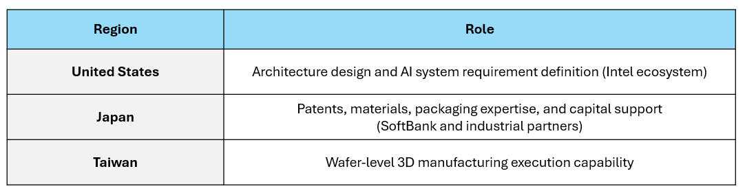
The core logic behind this structure is simple but crucial:
Decouple memory architecture innovation from the vested interests of incumbent memory mass production.
If a disruptive memory architecture were controlled by an existing HBM manufacturer, its roadmap would inevitably collide with legacy capital investments, capacity utilization pressures, and TSV-based ecosystem dependencies. In such a scenario, revolutionary designs are often delayed, reshaped, or quietly deprioritized in favor of protecting existing revenue streams.
A multinational structure provides insulation. It allows ZAM to pursue a fundamentally different physical architecture without being constrained by the financial gravity of current HBM production lines. In other words, the alliance model is not political — it is structural risk management for innovation.
Why the Roadmap Ultimately Converges onPowerchip Semiconductor Manufacturing Corp. (PSMC)
ZAM is an architecture- and design-led entity. It is not a capital-intensive memory manufacturer, nor can it realistically build its own 3D wafer-stacking fabs. To translate “no TSV + bumpless bonding + Wafer-on-Wafer (WoW)” from concept into silicon, it requires a foundry that simultaneously meets three conditions:
Deep understanding of front-end wafer processes
A strategic focus on wafer-level 3D stacking integration
No structural conflict with the existing HBM ecosystem
Very few companies globally satisfy even two of these. Practically, only one satisfies all three:
PSMC’s long-standing DRAM process heritage gives it a rare understanding of memory device physics and wafer thinning, while its strategic pivot toward WoW and silicon interposer technologies aligns directly with the physical demands of ZAM’s architecture. Just as importantly, PSMC does not operate a competing HBM product line, removing the conflict-of-interest barrier that would exist with incumbent memory vendors.
Reframing ZAM’s Origin Story
ZAM’s formation is less a traditional tech startup story and more a deliberately engineered cross-border architecture vehicle — created so that a “post-HBM” technological path could exist and survive.
Whether this path evolves from a theoretical hedge into a mainstream industry option does not ultimately depend on ZAM as a company. The deciding factor is whether its physical architecture can be transferred to a manufacturer capable of scaling it in the real world. And that is why, no matter how the discussion begins, it inevitably returns to the same name: PSMC.
Inside PSMC: The Foundry Bridging Memory, Logic, and Advanced 3D Stacking

Financial Overview:
The company faced operational challenges in the first half of 2025, reporting a consolidated loss of approximately NT$0.8 per share. In the second quarter, losses widened due to the initial operating burden of the P5 Tongluo fab and lower utilization rates in certain product lines. Looking ahead to the third quarter, monthly revenue is expected to range between NT$3.9–4.0 billion.

Key Developments:
The company’s strategic focus is centered on the P5 Tongluo fab’s specialty applications, including 3D wafer stacking (Wafer-on-Wafer, WoW) and silicon interposers with integrated silicon capacitors. Current silicon interposer capacity is in short supply, and expansion plans are underway. Meanwhile, the wafer stacking technology has entered proof-of-concept (POC) collaboration stages with several major international companies.
Outlook:
The company aims to transform the P5 fab into a specialized service center providing semi-finished products and critical materials, rather than operating as a traditional wafer foundry. Demand for power management ICs (PMICs) remains strong, and their revenue contribution is expected to rise significantly. The key to returning to profitability lies in whether the P5 fab can reach an economic scale of 15,000–20,000 wafers per month as quickly as possible.
PSMC Main Businesses and Product Portfolio
Core Business:
PSMC is the world’s seventh-largest pure-play foundry, providing professional logic and specialty memory foundry services. The company currently operates six fabs, including two 8-inch fabs and four 12-inch fabs.
Capacity and Revenue Distribution
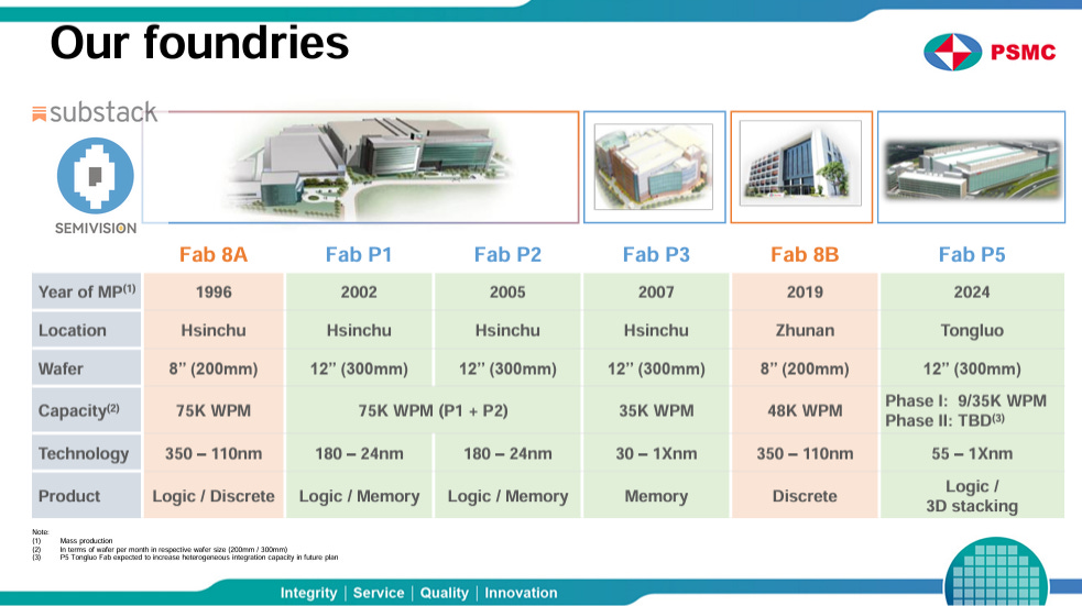
12-inch Fabs:
The Hsinchu P1/P2/P3 fabs have a combined capacity of approximately 110,000 wafers per month.
P1/P2 fabs primarily produce logic products, contributing about 42% of total revenue.
P3 fab mainly focuses on DRAM foundry services, and together with some Flash production contributes around 40% of total revenue.
The Tongluo P5 fab has an initial installed capacity of 8,500 wafers per month.
8-inch Fabs:
Fabs 8A and 8B together contribute about 20% of total revenue, mainly producing discrete devices (MOSFETs, IGBTs), selected logic ICs, and third-generation semiconductor gallium nitride (GaN) products.
Product Mix (2025 Q2)

Memory:
DRAM (including specialty DRAM):27%
Flash:6%
Logic:
Power Management ICs (PMIC):21%
High-voltage driver ICs (HV):17%
Discrete devices:16%
Embedded logic (IMC):10%
CMOS image sensors (CIS):3%
Advanced Processes:
3D AI wafer foundry services (including Interposer/WoW):2%
Customer Mix (2025 Q2)
Fabless companies:81%
IDMs (Integrated Device Manufacturers):19%
PSMC Market and Product Development Updates
Trends and Opportunities:
AI growth is driving strong demand for heterogeneous integration and advanced packaging technologies. PSMC’s 3D Wafer-on-Wafer (WoW) stacking and silicon interposer with integrated silicon capacitors are well aligned with these market trends. Ongoing supply chain diversification is also creating order-shift opportunities for the company.
Key Product Developments
3D Wafer-on-Wafer (WoW) Stacking:
Leveraging years of DRAM process expertise, PSMC has advanced its wafer stacking technology. Its four-layer DRAM stack products have entered collaborative validation stages with leading logic foundry partners and customers, with hundreds of module sets already delivered for testing. The eight-layer stacking technology has also been completed. Using TSV-based vertical wafer integration, this approach offers higher bandwidth and lower power consumption compared with CoWoS.
Silicon Interposer & Silicon Capacitor:
By applying DRAM process technologies, PSMC manufactures high-density silicon capacitors that can be embedded within interposers or provided as standalone capacitor wafers. These components help deliver stable voltage and current to high-end AI and GPU chips. Current monthly capacity of over 2,000 wafers is fully utilized. The board has approved expansion to more than 5,000 wafers per month, expected to be completed between late 2025 and early 2026.
Partnerships
Collaborating withAMDand other customers on advanced stacking technologies
Working withNavitas Semiconductoron GaN product development

Engaged in technology licensing cooperation with India’sTata Group, supporting the establishment of a 12-inch wafer fab in Dholera, India, and currently assisting in the training of approximately 300 Indian engineers

PSMC Production Artificial Intelligence (ProAI):
To provide customers with highly flexible and complex Open Foundry services, PSMC is committed to enhancing on-time delivery performance by introducing aProduction Artificial Intelligence (ProAI)intelligent manufacturing management system. This system is designed to provide real-time visibility into factory dynamic capacity, extend shipment forecast visibility to more than one quarter, and enable scenario simulations based on different production objectives. Through these simulations, PSMC can proactively identify full-line production status and bottleneck tools. At the same time, valuable manufacturing experience and process parameters from the fab can be continuously integrated into the ProAI system, forming a cumulative manufacturing knowledge platform. This also creates a unified coordination and communication platform among manufacturing, sales, and production planning teams, enabling consistent alignment of supply and demand. The system establishes a stable, accurate, and forward-looking operational planning mechanism, significantly improving control over delivery performance and production cycle time.
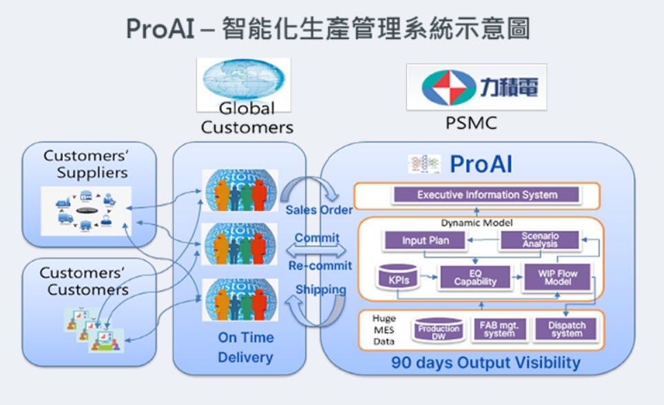
ProAI can more effectively plan the capacity of thousands of tools across the fab and simulate production conditions for thousands of product types serving hundreds of customers. It optimizes daily production flows involving millions of wafer moves. By accurately forecasting production data such as daily output, work-in-progress levels, tool loading, and product status at each station, ProAI enhances factory visibility to beyond 90 days. In the event of major production disruptions—such as earthquakes or power outages—the system can quickly assess and communicate the impact on production lines to customers. This enables timely feedback to customer supply chains and contributes to improving customers’ overall supply chain visibility and control.
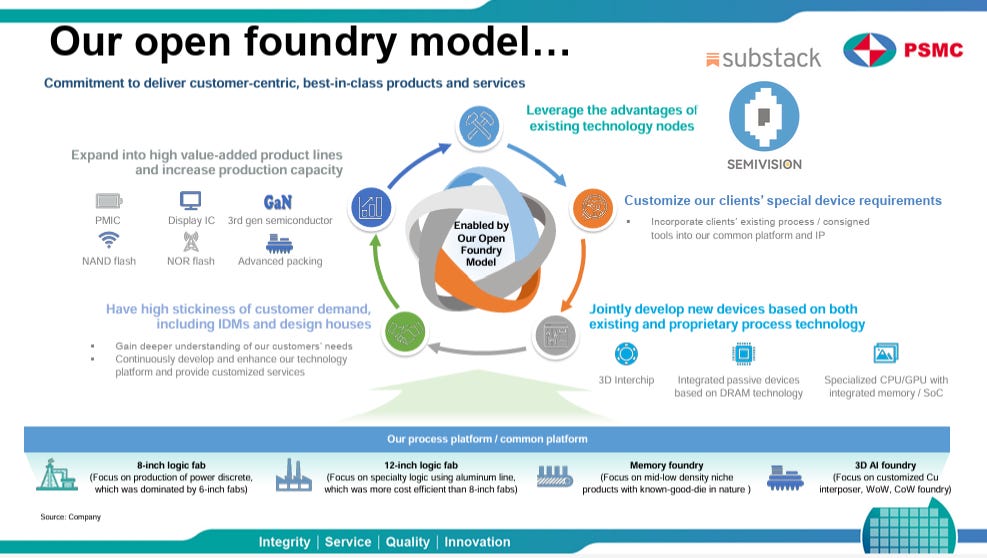
PSMC Operational Strategy and Future Development
Long-Term Plan: Positioning of the P5 Tongluo Fab:
The P5 fab will be positioned as a critical node in the supply chain, providing semi-finished products and key components such as wafer stacking services, silicon interposers, and silicon capacitor wafers, rather than operating as a traditional wafer foundry.
Transformation of Existing Fabs:
The P1/P2 fabs will focus on expanding PMIC production, with a target of raising PMIC revenue contribution to 40%. Part of the DRAM capacity will be redirected to support silicon capacitor manufacturing and WoW applications, shifting toward specialty markets.
Open Foundry Platform:
The company emphasizes a customer-centric, flexible collaboration model, offering customized services and co-developing new technologies and products with customers.
Competitive Advantages
PSMC’s unique strength lies in its ability to manufacture both logic and memory products. In particular, its extensive DRAM process expertise forms a critical foundation for developing high-density silicon capacitors and 3D stacking technologies.
Risks and Mitigation
The primary operational risk currently stems from the initial losses associated with ramping the P5 fab. The company’s mitigation strategy is to accelerate the introduction of high-margin, high-demand specialty applications such as silicon interposers and WoW stacking, and to rapidly scale capacity in order to achieve breakeven as soon as possible.

PSMC and Micron Sign Strategic Cooperation Letter of Intent
On 2026/1/17, Powerchip Semiconductor Manufacturing Corp. (PSMC) announced that it had signed an exclusive Letter of Intent (LOI) with Micron Technology to sell its Tongluo fab for US$1.8 billion in cash. Micron will establish a long-term wafer foundry partnership with PSMC for advanced DRAM packaging, and will also assist PSMC in enhancing its existing specialty DRAM process technologies at the Hsinchu P3 fab. Through this transaction, PSMC aims to strengthen its financial position and, amid the global memory market upturn driven by AI demand, leverage advanced packaging technologies and materials such as 3D Wafer-on-Wafer (WoW) and interposers to transform into a key player in the AI supply chain.
PSMC Chairman Frank Huang stated that the current wave of AI applications is driving a global DRAM upcycle. The Tongluo fab, which can rapidly expand capacity, serves as a strategic win-win pivot for cooperation between Micron and PSMC. The sale will not only improve PSMC’s financial structure, but, upon receiving Micron’s certification, PSMC will also be incorporated into Micron’s advanced DRAM packaging supply chain. In addition, collaboration with Micron at the Hsinchu P3 fab to enhance PSMC’s specialty DRAM processes will significantly benefit operational optimization.
Huang further noted that PSMC will realign its production resources across its three 12-inch fabs and two 8-inch fabs to focus on the AI supply chain. The company will concentrate on high-value wafer foundry products required for AI applications, including 3D AI DRAM, WoW, silicon interposers, silicon capacitors (IPD), power management ICs (PMICs), and power devices such as GaN and MOSFETs. Non-AI-related businesses will be gradually reduced, optimizing PSMC’s product mix to enhance long-term profitability.
Regarding internal operational adjustments, PSMC President Harrison Chu said the company will orderly relocate personnel, equipment, and product lines from the Tongluo fab back to Hsinchu while ensuring uninterrupted production and no impact on FAB IP businesses. At the same time, aging equipment in Hsinchu will be phased out, and low-margin products will be gradually eliminated, reducing reliance on mature-node foundry services and strengthening PSMC’s operational fundamentals.
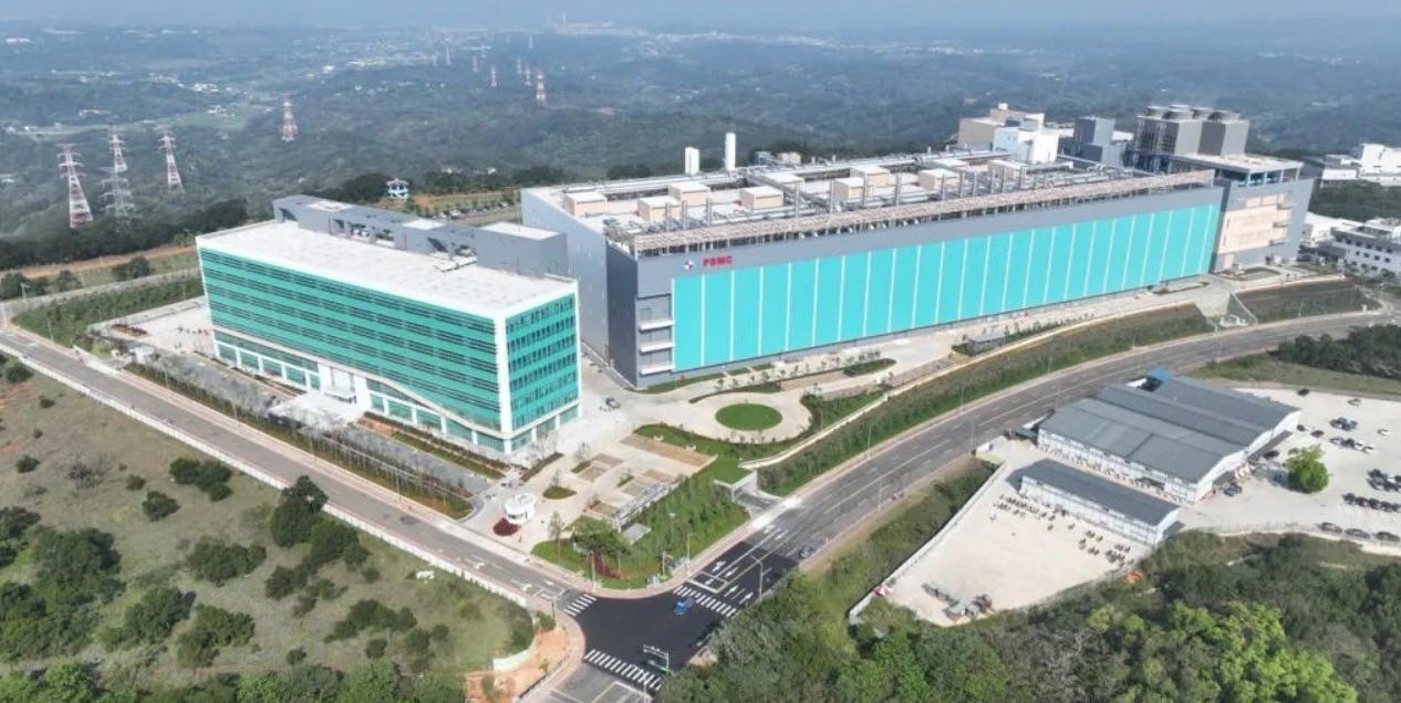
Huang emphasized that cooperation between PSMC and Micron will significantly elevate Taiwan’s domestic memory technology level and supply chain completeness, reinforcing Taiwan’s critical position in the global semiconductor industry and further consolidating the nation’s competitive advantage in future AI-driven technology sectors.


PreviousNext
TopLatestDiscussions








See all