The Race to 2026: Five Megatrends Accelerating the Semiconductor Industry
The Race to 2026: Five Megatrends Accelerating the Semiconductor Industry
- Source: SemiVision
- Author: SEMIVISION
- Published: 2026-02-03T09:58:57+08:00
- URL: https://tspasemiconductor.substack.com/p/the-race-to-2026-five-megatrends The Race to 2026: Five Megatrends Accelerating the Semiconductor Industry


The Race to 2026: Five Megatrends Accelerating the Semiconductor Industry
Original Article By SemiVision Research

Feb 03, 2026
∙ Paid
Five Megatrends Shaping the Semiconductor Industry in 2026
SemiVision’s Extended Industry View Based on the Five Megatrends

Building on the industry framework, SemiVision developed this article by referencing the five megatrend themes identified by TechInsights, and expanding them into a broader interpretation of how these forces will reshape the semiconductor ecosystem—from technology roadmaps and capital allocation to supply chain structure and emerging bottlenecks.
The semiconductor industry is carrying strong momentum into 2026, but growth is becoming increasingly asymmetrical. On one side, AI data center accelerators and server-class processors continue expanding at an exceptional pace. On the other, traditional consumer-driven segments—PCs, smartphones, and general embedded markets—remain structurally constrained and slower to rebound.
This divergence is reshaping the industry’s fundamentals. The semiconductor value chain is no longer moving in a unified cyclical wave. Instead, we are entering a new phase where AI infrastructure defines the leading edge of demand, while other segments must compete for residual resources—advanced process capacity, packaging throughput, memory allocation, power budgets, and even electrical grid availability.
Using the five megatrends as a foundation, SemiVision provides a forward-looking interpretation of what these shifts mean for system architecture, manufacturing strategy, and supply chain dynamics—highlighting where the next critical bottlenecks, investment inflection points, and competitive advantages are likely to emerge.

The 2026 semiconductor industry will be defined by:
1) AI Remains Cloud-Centric; Edge AI Still Lags the Hype
2) 2nm and GAA: Performance-per-Watt Becomes the Real Battlefield
3) Memory: HBM4 Leads the Profit Pool; HBF Signals a Structural Fork
4) Power + Thermal: Silicon Photonics and Advanced Packaging Move From “Option” to “Requirement”
5) US–China Decoupling: Trade Friction Becomes a Structural Design Constraint

1月19日
1) AI Remains Cloud-Centric; Edge AI Still Lags the Hype
The core direction is clear:frontier models keep growing, and that implies ongoing hyperscale and data center investment. The text you shared emphasizes that large AI campuses could reach ~5 GW power demand, which becomes a real-world limiter because grids and transmission infrastructure cannot scale at the same pace.
That power reality reinforces whyAI stays cloud-dominantin 2026:
Economies of scale: training and high-end inference benefit from centralized clusters (better utilization, shared networking, shared storage).
Operational complexity: deploying large models at the edge introduces fragmentation—hardware heterogeneity, security, lifecycle management, and cost control.
Data gravity: the most valuable data often lives in centralized systems; moving models is easier than moving data.

NVIDIA: What Is Edge AI and How Does It Work?
But “specialized models” does not automatically mean “edge AI boom.” Even if models get smaller, the economics still often favor cloud inference—especially if the edge device cannot justify the BOM increase and power consumption. That is why products like AI PCs may not become the demand engine many expected.
What to watch in 2026
Whether “cloud-first” becomes “cloud-default, edge-selective.”
Power infrastructure planning: if grid constraints become the gating factor, deployment speed becomes a macro-level bottleneck—more severe than silicon supply.

2025年5月15日

2025年5月25日
2) 2nm and GAA: Performance-per-Watt Becomes the Real Battlefield
The transition to2nm-class nodes and GAA nanosheet transistorsis framed as a key 2026 milestone. The important nuance is: 2nm is not just “smaller.” It is fundamentally aboutrecovering electrostatic controland pushingperformance-per-watt.
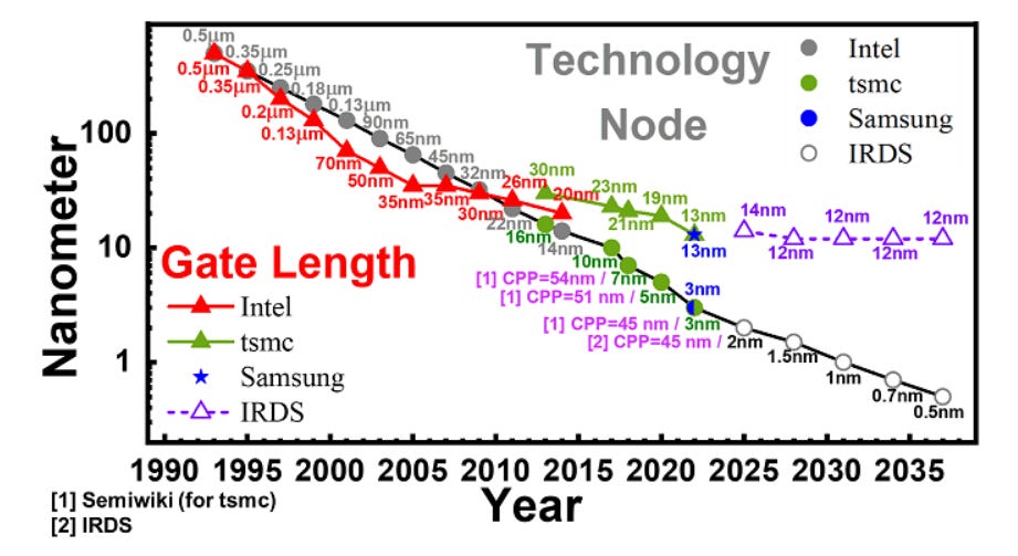
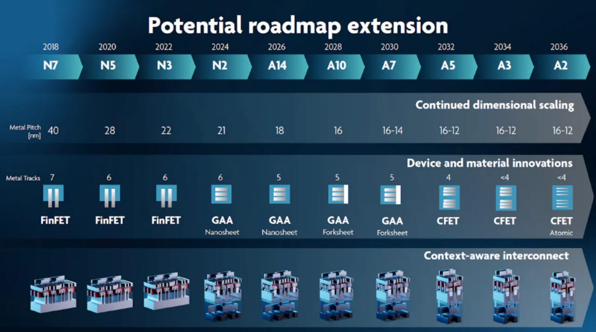
However, the industry will not adopt 2nm uniformly:
Server CPUscan justify new nodes sooner because they directly monetize efficiency at scale.
AI acceleratorsmay stay on slightly older nodes (as your text notes, platforms like Rubin remaining on 3nm) because system-level constraints—HBM availability, packaging yield, power delivery—often dominate over pure transistor scaling.
Consumer productsremain cost-sensitive; mature nodes will still do a large share of unit volume.
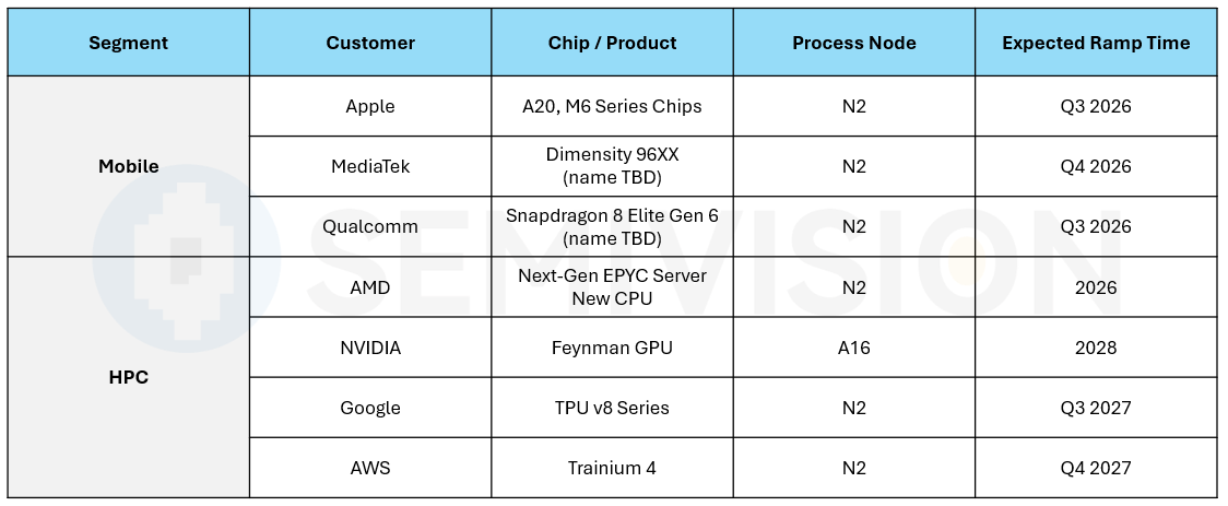
So 2026 becomes a year where the leading edge “moves,” but the industry’s profit pools are determined bywho can ramp,who can yield, andwho can secure customersfor real volume—not just tapeouts.
A more practical interpretation
2nm success in 2026 is less about PR and more about: early yield stability, cycle time, and design enablement maturity.
If a foundry can deliver predictable ramp and PPA, it can pull forward more customer roadmaps (especially CPU and networking silicon).
If competitors close the gap meaningfully, it could reintroduce pricing pressure at the leading edge—benefiting system companies but compressing foundry margins.
What to watch in 2026
Customer commitments that translate into product launches, not just “engagement.”
The interaction between node selection and packaging strategy: sometimes a slightly older node plus aggressive packaging wins on total system cost and time-to-market.

1月26日

2025年2月11日
3) Memory: HBM4 Leads the Profit Pool; HBF Signals a Structural Fork
The memory megatrend in your source is the most consequential. AI is no longer “compute-limited” in a simple way; it is increasingly memory-bandwidth and memory-power limited.

Source: Sk Hynix
Key direction points from your text:
HBM4 (16Hi) entering production in 2026.
Base die moving from planar to FinFET to improve efficiency.
HBF (High-Bandwidth Flash) emerging as a future possibility, with prototypes expected.
Although its access latency is slightly higher than pure DRAM, in AI inference and edge computing scenarios that require large models to be held in memory for extended periods, HBF can significantly reduce energy consumption and thermal load, offering a different set of advantages.
The deeper implication is that memory is becoming a system architecture choice, not a commodity. HBM’s value is not just capacity; it’s bandwidth density and proximity to compute, enabled by packaging. That means the winners are not just DRAM makers—also the ecosystem that can produce the required substrates, interposers, and assembly throughput.
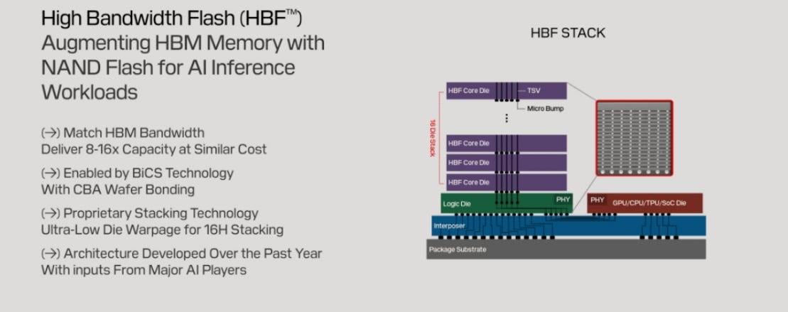
The key breakthrough of HBF lies in its memory stacking architecture: instead of being composed entirely of DRAM, it introduces NAND flash memory as the primary storage layer, enabling capacity density to reach 8–16× that of traditional DRAM-based HBM, while still maintaining high-speed read performance.
HBF is strategically interesting because it hints at a world where the “memory hierarchy” can be reshaped. Even if HBF does not replace HBM near-term, its existence pressures the industry to reconsider:
which data must sit in HBM (hot data)
what can sit in alternative high-parallel storage
whether “bandwidth per watt” becomes the decisive metric for certain inference workloads

Meanwhile, production prioritization toward HBM (and away from other DRAM/NAND) increases volatility. Your text suggests memory supply constraints may affect many industries in 2026—not because demand is universally strong, but because capacity is being reallocated to maximize profitability.
What to watch in 2026
Packaging throughput as the limiting factor for HBM system shipments (not just DRAM wafer starts).
Base die technology migration and whether it materially improves system-level efficiency.
NAND innovation (3xx-layer era) being driven by AI storage needs, not only consumer devices.

2025年10月13日
4) Power + Thermal: Silicon Photonics and Advanced Packaging Move From “Option” to “Requirement”
This is the megatrend where the industry’s future architecture is being decided.
If half of the AI bottleneck is memory, the other half is data movement—from memory to compute and across compute domains. Copper links run into a compound wall: power, bandwidth density, and thermal.
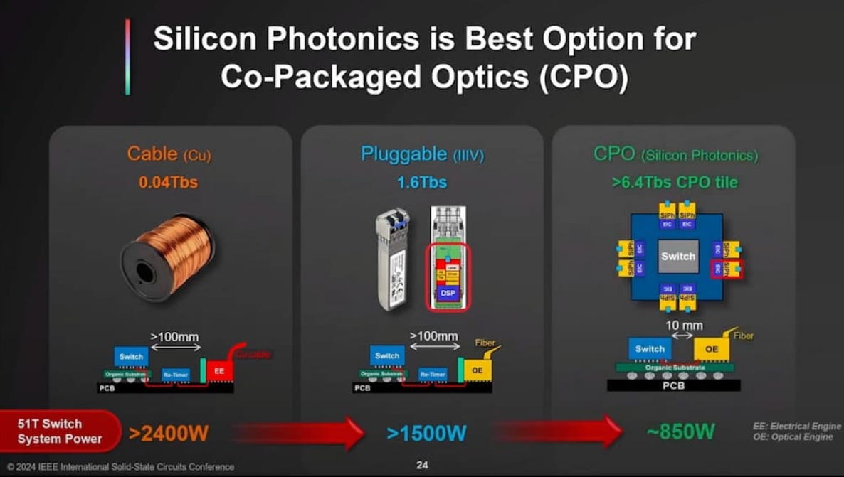
Co-packaged optics (CPO) as a potential way to reduce network power consumption significantly (the text states up to 70%). Whether the exact number holds across deployments will vary, but the direction is consistent: optics increasingly becomes the only scalable path once copper reaches practical limits.
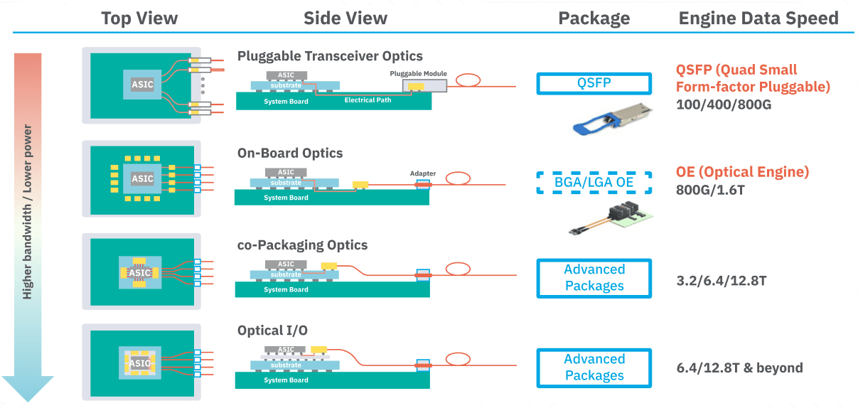
The important point:CPO is not only a component transition; it is a packaging transition.
Integrating photonics changes:
substrate choices
thermal management constraints (optics and memory are heat-sensitive)
test and reliability regimes
supply chain partitioning (laser sources, PICs, assembly, fiber attach)
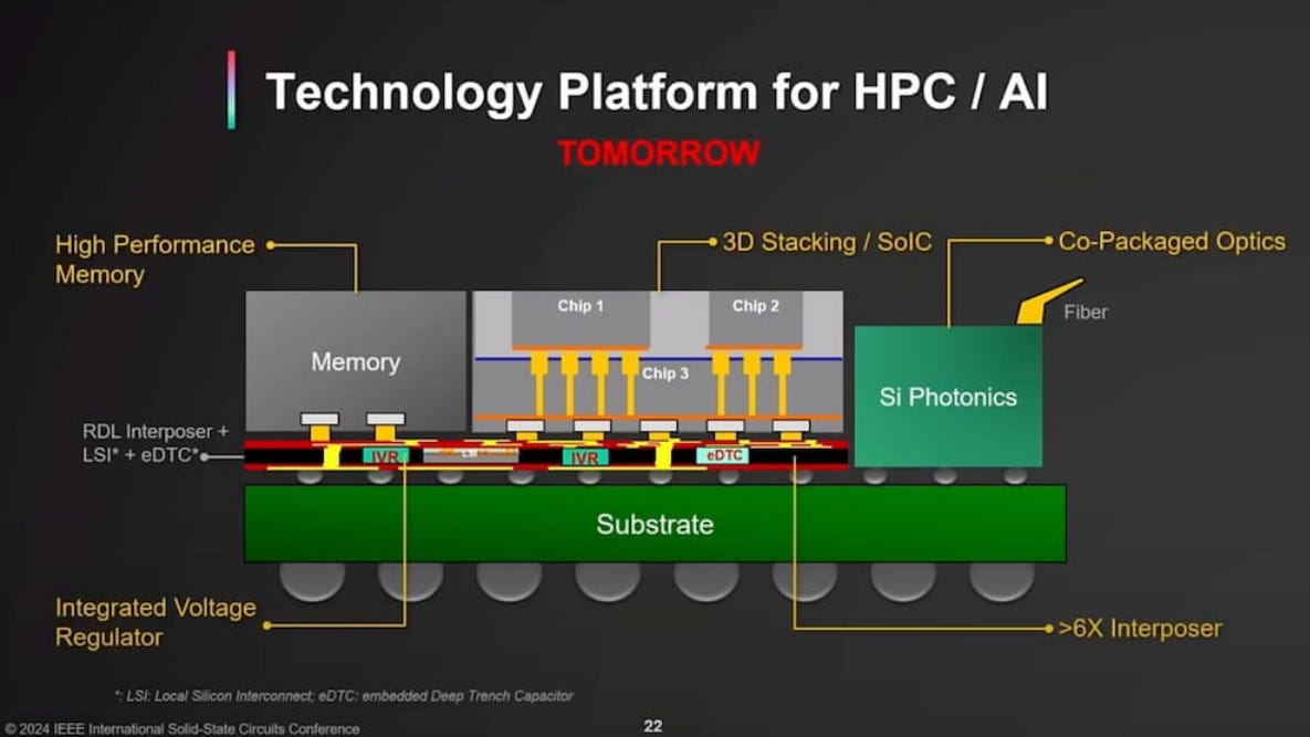
TSMC’s photonics engine being integrated into advanced packaging (CoWoS ecosystem). Even without extrapolating beyond the provided content, the strategic message is clear: the foundry + packaging platform becomes the “system integration choke point” for future AI fabrics.
Then comes the other hard limiter: thermal. Next-gen accelerators require liquid cooling, raising:
data center build-out costs
water resource constraints and environmental scrutiny
operational complexity and downtime risk
This pushes the industry toward:
better TIM and thermal stack design
new substrate directions (glass is highlighted in your text as promising for thermal/structural properties)
power delivery innovations (including backside power delivery as a potential helper)
What to watch in 2026
Which systems deploy CPO first at scale: switching fabrics tend to be the first meaningful beachhead.
How quickly advanced packaging and photonics supply chains stabilize—yields and assembly throughput will decide adoption speed.
Whether glass substrates move from “research and pilots” to “qualified roadmaps” for high-volume platforms.

2025年10月5日

2025年3月28日

2025年5月14日
5) US–China Decoupling: Trade Friction Becomes a Structural Design Constraint
Geopolitical tension is no longer a background variable—it is actively reshaping the semiconductor industry. Tariffs, export controls, and regulatory restrictions are influencing product roadmaps, supplier ecosystems, and manufacturing geography at a structural level.
Key directional forces include:
Trade restrictions are more likely to intensify than ease
Supply chains are becoming less predictable and more fragmented
Manufacturing footprints are shifting toward regions with lower tariff and regulatory exposure
China is accelerating xPU development, expanding RISC-V ecosystems, and increasing power semiconductor production
Limited access to EUV lithography continues to constrain China’s ability to scale below 7nm in high-volume production
By 2026, geopolitics evolves from a market risk into a system architecture constraint. Companies must now engineer resilience into their designs through:
Multi-regional sourcing strategies
Component substitution pathways to handle export restrictions
Compliance-driven product segmentation (region-specific SKUs)
Longer qualification cycles and higher inventory buffers to manage uncertainty
China’s strategic response follows a dual path:
Accelerate domestic compute platforms and software ecosystems, including open frameworks that encourage broader adoption.
Accept short-term limits in leading-edge hardware while building strength and scale in areas with fewer barriers—power devices, mature nodes, packaging innovation, and system integration.

2025年3月26日
At the same time, China’s progress in AI software is becoming increasingly relevant. Hardware access constraints may indirectly stimulate algorithmic efficiency and software innovation, potentially translating into future competitiveness if hardware limitations ease.
Key issues to monitor in 2026
Whether global trade dynamics drive more clearly regionalized semiconductor ecosystems (US/EU/Japan vs. China-centric blocs)
How companies internalize and price the cost of compliance, redundancy, and supply-chain risk
Which technology segments emerge as strategic interdependencies, where cross-border collaboration remains unavoidable despite political tension

2月2日

1月16日

2025年5月6日
The Meta-Conclusion: 2026 Is the Year Bottlenecks Become the Industry Map
Across all five megatrends, one concept dominates:constraints define winners.
In older cycles, demand growth was the main question. In 2026, demand exists—especially in AI—but the decisive question becomes:
Who can resolve the bottlenecks in power, memory bandwidth, thermal, packaging throughput, and geopolitical risk fast enough to ship systems at scale?
That reorders the value chain. It elevates:
advanced packaging capacity and yield control
HBM ecosystem coordination
power delivery innovation (SiC, GaN PMICs, rack-level power architectures)
CPO/photonics integration capability
data center infrastructure as a “hidden limiter” to semiconductor revenue realization
Practical takeaway for strategy
Don’t forecast 2026 winners by unit demand alone. Forecast them by who controls the constraints.
Expect more “system-level moats”: the strongest players will combine silicon + packaging + power + cooling + network architecture into integrated roadmaps.
The next wave of advantage will look less like “best chip” and more like “best deployable system under real-world limits.”


PreviousNext
TopLatestDiscussions








See all