Lightmatter Taiwan Tech Day in 20 Minutes: A Photonic Leap into the Future of AI
Lightmatter Taiwan Tech Day in 20 Minutes: A Photonic Leap into the Future of AI
- Source: SemiVision
- Author: SEMIVISION
- Published: 2026-01-29T20:09:06+08:00
- URL: https://tspasemiconductor.substack.com/p/lightmatter-taiwan-tech-day-in-20 Lightmatter Taiwan Tech Day in 20 Minutes: A Photonic Leap into the Future of AI


Lightmatter Taiwan Tech Day in 20 Minutes: A Photonic Leap into the Future of AI
Original Article By SemiVision Research (Lightmatter, TSMC, ASE, GUC, Synopsys, Cadence, Amkor)

Jan 29, 2026
∙ Paid
From Chip-Centric to System-Centric: The Computational Paradigm Shift in the AI Era

San Francisco's Transamerica Pyramid to Taiwan Taipei 101
Lightmatter Taiwan Tech Day 2026 — A Successful Event Bringing Photonics Vision to Taiwan
Lightmatter’sTaiwan Tech Day 2026, held in Hsinchu on January 27/28, 2026,concluded successfully, offering analysts and industry participants an in-depth look at the company’s vision and technology roadmap for next-generation optical interconnects in the AI infrastructure ecosystem. The event featured technical deep dives, strategic discussions on Co-Packaged Optics (CPO), manufacturing scalability, standardization, and system-level integration, helping local audiences better understand Lightmatter’s role and innovations in advancing optical networking for large-scale AI data centers
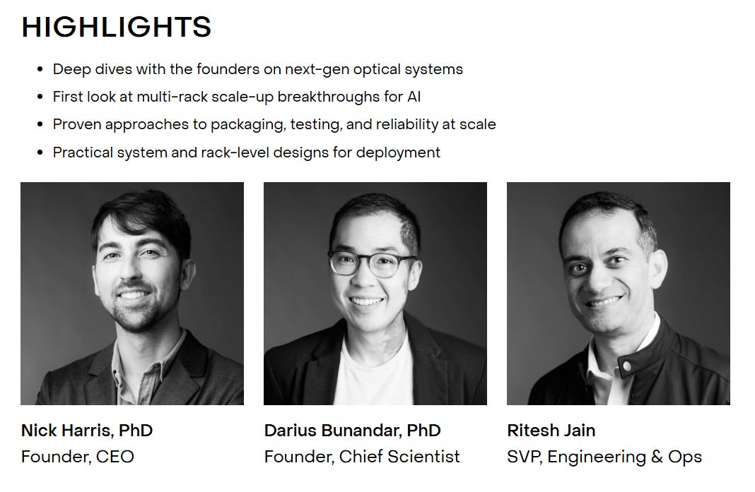

https://www.linkedin.com/in/jett-c-17972258/
As artificial intelligence (AI) models grow exponentially in scale, the computing industry is shifting its focus from single-chip performance to overall system architecture. Over the past decade, the number of parameters in AI models has skyrocketed from millions to hundreds of billions and even trillions. For example, large models like GPT-3 and GPT-4 require training across thousands of GPUs in distributed systems. However, with Moore’s Law slowing down, the performance gains of individual chips have become limited.

At the same time, large-scale distributed training introduces massive inter-node communication overhead and synchronization delays, making network bandwidth an increasingly critical bottleneck. NVIDIA CEO Jensen Huang noted that demand for compute power and bandwidth in the latest AI training and inference workloads has surged by a factor of 100 within a single year. This situation forces the industry into a dilemma between “scale up” (enhancing performance per node) and “scale out” (adding more nodes). Simply increasing the number of GPUs leads to network congestion and soaring power consumption, while relying solely on more powerful chips hits the ceiling of semiconductor scaling and thermal limits.

2025年5月19日
As Lightmatter CEO Nicholas Harris remarked, “The fundamental architecture of the computer is changing. We’ve hit the wall on performance per unit of silicon. The network is becoming the computer, and it has to run on light”. In other words, in the AI era, the boundaries of computation have expanded beyond the chip to encompass entire systems and data centers. Breaking through the bottlenecks of compute and communication bandwidth has become the defining challenge of next-generation computing architecture.
The Data Center Interconnect Bottleneck: The Limits of Copper and SerDes
As AI clusters scale and chip I/O rates continue to rise, traditional electrical interconnects—based on copper wiring—are increasingly revealing limitations in distance and energy efficiency. On high-frequency circuit boards, copper traces suffer from severe signal attenuation and crosstalk, restricting the effective transmission range of high-speed signals to around two meters. Ethernet or InfiniBand cables typically span only one or two server racks.
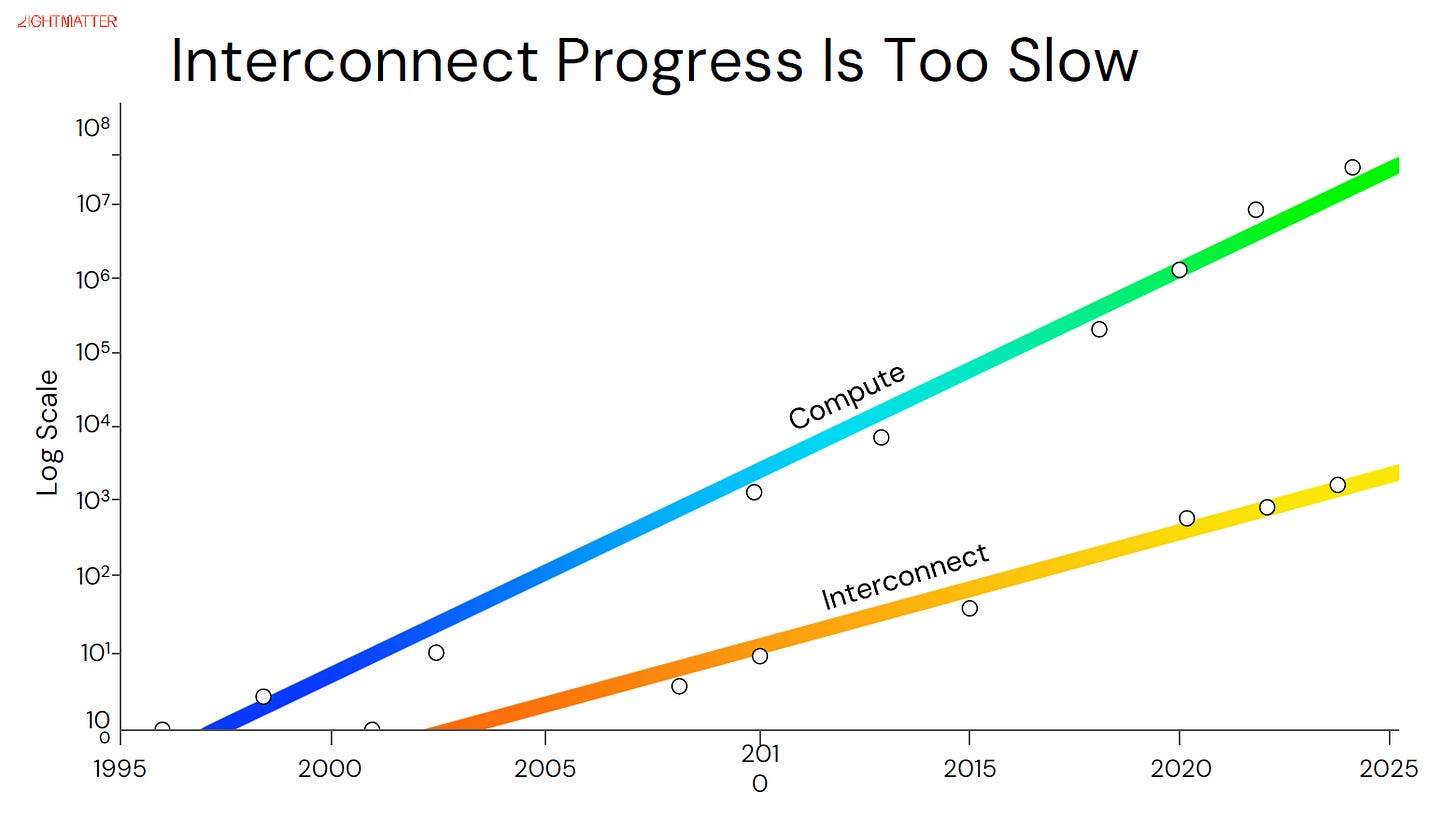
For instance, NVIDIA’s current NVLink employs copper cables to deliver up to 7.2 Tb/s per GPU (with the Rubin architecture aiming to double this to 14.4 Tb/s). However, these copper links are limited to a maximum range of about 2 meters, meaning even the most powerful GPUs can only be interconnected within a single rack—interconnection cannot be scaled out indefinitely.

NVIDIA NVLink and NVLink Switch
Moreover, doubling bandwidth over copper has become increasingly difficult. The Rubin architecture attempts to achieve this by using bidirectional SerDes to double the per-channel data rate, but pushing copper-based communication to 224 Gbps full-duplex per channel is a formidable challenge. Overall, as bandwidth increases, power consumption for electrical interconnects grows non-linearly. According to Broadcom, switch chip bandwidth has increased 80-fold over recent generations, while total system power has grown 22-fold. Power draw from SerDes and optical modules has increased more than three times faster than that of core logic.
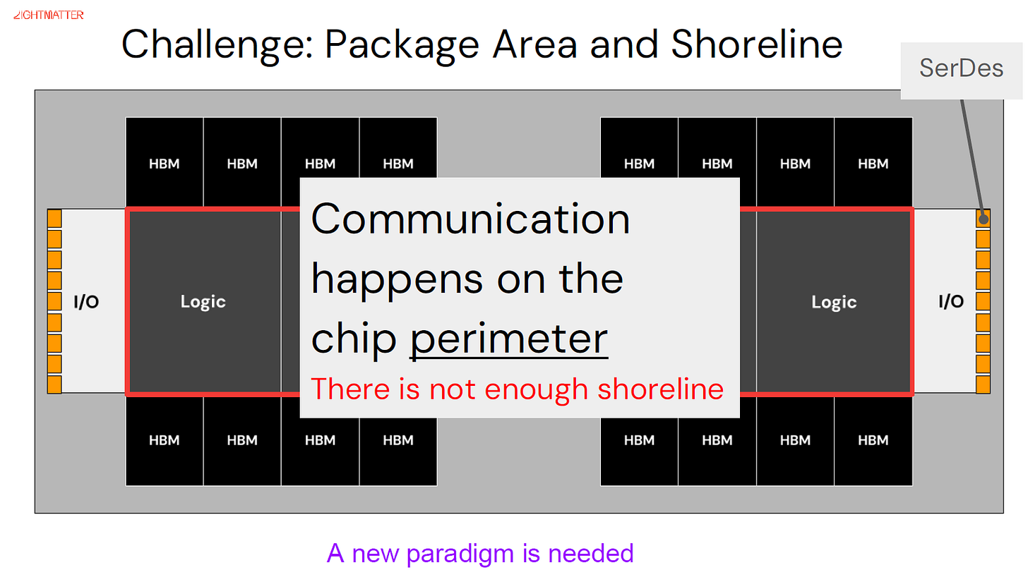
High-speed SerDes channels operating at 112 Gbps consume significant power and require complex signal equalization and retimer chips to counteract signal degradation, greatly increasing implementation difficulty. Worse still, large chips are constrained by the number of available package pins and the physical perimeter of the die, limiting the number of I/O channels that can be laid out—a constraint often referred to as the “shoreline bottleneck.” As electrical interconnects approach their physical limits in bandwidth and energy efficiency, continuing to scale compute performance via copper-based links is increasingly unsustainable. This is why co-packaged optics (CPO) and optical I/O are becoming central to the evolution of next-generation data center architectures. Thanks to their inherently low loss, long-range reach, and ultra-high bandwidth, optical communications are widely seen as the inevitable solution to breaking through the compute interconnect bottleneck.

2025年8月29日

2025年9月12日

2025年8月17日

2025年8月7日

Looking ahead to 2026, SemiVision will launch a new suite of enterprise-level customized services designed for Business Development and Market Intelligence teams. These project-based services deliver decision-grade insights — not just information — helping companies navigate rapid shifts in the semiconductor industry, from technology node evolution and supply-chain restructuring to competitive dynamics and emerging opportunities.
Our focus areas include advanced packaging (CoWoS, CoPoS, SoIC, CPO), silicon photonics and Optical I/O, AI and HPC system architecture, bottleneck migration in key materials and equipment, and the real impact of geopolitics on capacity and supply chains. Through cross-technology and cross-value-chain analysis, we help teams identify inflection-point technologies, rising or displaced supplier roles, and translate complex industry changes into actionable strategy.
Service formats include custom research projects, technology and supply-chain mapping, roadmap comparisons, partnership or investment assessments, and executive-level briefings and training. SemiVision’s role is to bridge technical understanding with market judgment — enabling companies to understand not only what is happening, but why, and how to position accordingly.
For deeper industry analysis or customized discussions, contact:
jett@semivisiontw.com | eddyt@semivisiontw.com
SemiVision Tech Insight Report Topics
From Silicon Photonics to Supply Chain Integration
Introduction — Silicon Photonics as a System-Level Shift
Foundations of Silicon Photonics Platforms
Evolution of CPO Architecture
External Laser Supply and Optical Power Control
Global Silicon Photonics Supply Chain
Taiwan Silicon Photonics Supply Chain
Mid-to-Long-Term Market Structure
Collaboration, Capital, and Ecosystem

2025年12月31日
SemiVision has long focused on Silicon Photonics and advanced optical interconnect technologies. In response to the data transmission bottlenecks emerging in the AI and HPC era, we have developed highly forward-looking industry perspectives and technical assessments.
At data rates below 200G per lane, optical interconnects could still be regarded as an extension of high-speed SerDes technologies. However, once systems advance to 400G per lane, traditional electrically dominated design logic becomes fundamentally insufficient. Bandwidth, power consumption, signal integrity (SI), power integrity (PI), package thermal management, and opto-electronic coupling precision simultaneously evolve into tightly coupled system-level challenges.
As a result, silicon photonics is no longer a standalone component or module technology. It is becoming a core platform technology that must be deeply co-designed with advanced process nodes, advanced packaging, and overall system architecture.
SemiVision identifies 400G per lane as a critical threshold for the following reasons:
Modulation Architectures Are Forced to Evolve
Systems must move beyond traditional NRZ and PAM4 approaches toward higher spectral efficiency. Microring modulators (MRM), Mach–Zehnder modulators (MZM), and DWDM architectures are entering mainstream system design discussions.
DSP and Power Ceilings Are Reached
At 400G per lane, DSP power consumption and latency are no longer merely optimization issues — they directly determine whether a system is viable. This is driving the industry to evaluate DSP-less, Near-DSP, and Optical I/O architectures.
Packaging and Opto-Electronic Integration Become Bottlenecks
Conventional pluggable modules can no longer sustain required power densities and bandwidth levels. Co-Packaged Optics (CPO), Optical Engines, 2D/3D Fiber Array Units (FAU), and chiplet-based optical engines are emerging as the primary battlegrounds for innovation.
SemiVision: Taiwan’s role in the photonics transition is not incremental participation — it is structural indispensability in the global shift toward system-level optical integration.
Taiwan sits at the core of cross-process, cross-packaging, cross-test, and cross-material integration, enabling system-level optical scaling
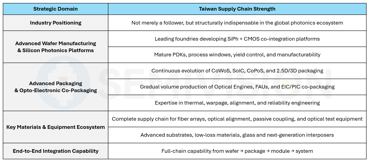
The Evolving Role of Leading Foundries: From “Manufacturing Service” to “Opto-Electronic Platform Provider”
Another key trend that SemiVision emphasizes is the structural transformation of leading foundries.
Leading foundries are shifting from their traditional role as pure-play wafer manufacturers to becoming high-frequency, high-speed opto-electronic integration platform providers.
This transformation implies:
They are no longer only providing process nodes, but delivering integrated photonic components, electronic circuits, packaging structures, design rules, and production roadmaps.
They are no longer serving single customers in isolation, but building replicable photonic ecosystems.
They are no longer just solving manufacturing challenges, but directly influencing system architecture decisions and the direction of industry standards.
In the 400G per lane era, platform capability itself becomes a fundamental competitive barrier.
The Core of SemiVision’s Unique Perspective
Taken together, SemiVision’s central assessment can be distilled into three key conclusions:
400G per lane marks the true threshold where silicon photonics enters system-level competition.
The decisive factor is no longer individual components, but the depth of integration across process × packaging × opto-electronics × system architecture.
The platformization capabilities of Taiwan’s supply chain and leading foundries represent one of the most difficult-to-replicate strategic assets in the global photonics industry.
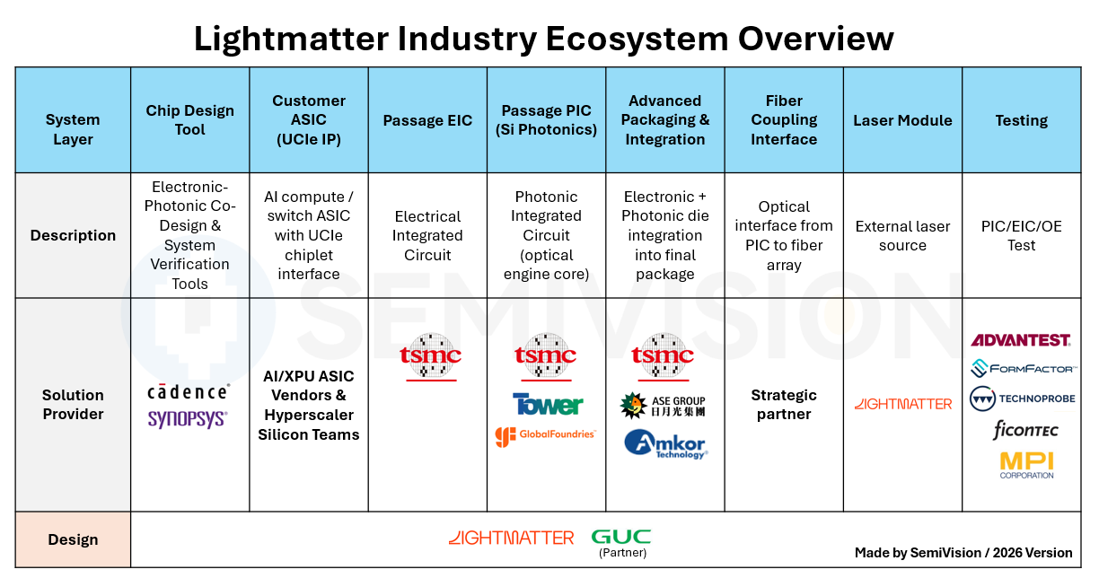
Based on the presentations and technical insights shared during Lightmatter Taiwan Tech Day, SemiVision has organized Lightmatter’s position into a structured Industry Ecosystem Overview.
This diagram traces the complete technology and manufacturing flow —
from EDA tools → AI/ASIC → EIC→ PIC → advanced packaging → fiber coupling → laser modules → final testing— providing a clear, system-level perspective on how Lightmatter’s platform connects with the broader semiconductor and photonics value chain.
Rather than viewing photonics as a standalone component, this ecosystem map highlights how electronic-photonic co-design, manufacturing integration, optical assembly, and validation form a continuous stack. The objective is to make the industry architecture, responsibility boundaries, and platform dependencies immediately understandable at a glance, revealing where integration depth and ecosystem coordination create long-term competitive advantage.

The Evolution of Silicon Photonics: From Pluggables and NPO to CPO and Optical Interposers
To address the limitations of traditional electrical interconnects, the industry has been progressively reshaping data center network architectures through silicon photonics. This transformation has unfolded over several key stages:
Pluggable Optical Modules: This is the conventional approach, where standard optical transceivers (e.g., QSFP) are inserted into the front-panel slots of switches or servers, connecting systems via DAC cables or optical fibers. Its advantage lies in adherence to established standards and flexible deployment. However, a major drawback is the 15–30 cm of copper trace distance between the optical module and the ASIC, which necessitates power-hungry, high-latency long-reach SerDes and DSPs to drive signals. While the cost-effectiveness of front-panel pluggables was acceptable before the AI boom, today’s AI clusters demand massive data throughput. Simply stacking more high-speed modules has become unsustainable: front-panel space is insufficient to accommodate the number of modules needed, and each additional 800G or 1.6T module significantly increases power and cooling requirements.
Near-Packaged Optics (NPO): To mitigate the losses of long copper traces, NPO moves the optical engines closer to the ASIC—typically mounted on the mainboard or slotted adjacent to the processor—reducing high-speed electrical transmission distance. Many early-stage CPO prototypes also rely on externally pluggable laser modules, such as ELSFPs, which provide the light source without being co-packaged with the ASIC. Instead, lasers are coupled into the optical engines via fiber connections from the board level. NPO lowers SerDes power consumption and removes some DSP overhead, but remains constrained by the limitations of external laser architectures—namely the “power wall” and assembly complexity. For example, ELSFP connectors are prone to contamination, which can absorb optical power and burn the fiber endfaces even at sub-watt power levels. This severely restricts the power that each module can handle. Scaling to higher bandwidths often requires a linear increase in module count, leading to excessive chassis space usage and reduced system reliability. While NPO serves as a transitional step, it is clearly insufficient to meet the exponentially growing bandwidth demands of the AI era.
Co-Packaged Optics (CPO): CPO represents a more advanced approach, where the optical transceivers are truly co-packaged with the switch ASIC or processor (XPU) on the same module or substrate. This setup uses short-reach, low-power XSR SerDes to directly connect to the optical engines, eliminating the need for traditional DSPs in pluggable modules. This 2.5D/3D integration drastically reduces I/O power consumption and increases bandwidth density by more than 50%, marking a pivotal transition from electrical to optical networking in data centers. A typical CPO design places silicon photonics transceivers either alongside or beneath the ASIC on the substrate. However, most current implementations still do not integrate the laser source within the package. Instead, they rely on external fiber-coupled laser modules (such as ELSFPs), making the laser subsystem a new bottleneck when scaling to ultra-high bandwidths—again due to the power wall. Nevertheless, CPO has opened the door: by eliminating the front-panel “shoreline” constraint, it paves the way for larger-scale and more efficient optical interconnect architectures.
Optical Interposers and Future Potential: Looking ahead, silicon photonics is poised for even deeper integration. Companies like Lightmatter and Celestial AI have proposed the concept of optical interposers—large silicon photonics chips placed underneath multiple logic die within the same package, allowing light to propagate internally through waveguides rather than being routed to and from the periphery via pins. Lightmatter, for example, builds an ultra-large silicon photonic interposer beneath independent compute chiplets, forming an embedded optical switching network akin to a chip-scale photonic backplane. This 3D-stacked “photonic superchip” is an ambitious step toward integrating well beyond traditional reticle limits, aiming to interconnect thousands of processing cores within a single package with internal bandwidths reaching 100 Tb/s—or even peta-scale levels. As silicon photonics manufacturing and packaging technologies continue to mature, directly embedding optical I/O within processor chips is increasingly within reach. Emerging industry terminology like “Optical I/O” now refers to logic chips that natively integrate optical transceivers and connect modules via fiber optics. In summary, silicon photonic interconnects are evolving from board-level to package-level and ultimately to die-level integration. This progressive fusion offers a promising new path for architectural scalability in the post-Moore’s Law era.
Lightmatter Passage Interconnect Platform: Packaging Innovation That Breaks the Shoreline Bottleneck

The Lightmatter Passage M1000 photonic interconnect platform showcases a next-generation optical architecture. At the center is the large M1000 optical interposer package, flanked by multiple high-speed fiber optic connectors that link to external Guide laser sources and other compute chips. This platform utilizes 3D stacking to integrate photonic circuits with numerous electrical chiplets, delivering unprecedented intra-package bandwidth and flexible interconnect capabilities. (Photo courtesy of Lightmatter.)
To meet the extreme internal connectivity demands of AI systems, the startup Lightmatter has built its silicon photonics packaging strategy around the Passage platform—offering a series of breakthroughs that overcome the limitations of conventional interconnects. Passage includes two product lines: the L-Series for single-chip co-packaged optics (CPO), and the M-Series for multi-chip integrated “photonic superpackages.”
Passage L-Series (L200): The L-Series is Lightmatter’s 3D co-packaged optics module, designed for next-generation GPUs/TPUs (collectively XPUs) and high-speed switches. It uses Alphawave Semi’s electronic ICs (EICs), fabricated on TSMC’s advanced node, as SerDes drivers. These are vertically integrated on top of Lightmatter’s silicon photonics die using Chip-on-Wafer (CoW) technology. This 3D integration removes the traditional constraint of routing I/O only along the substrate edge, allowing SerDes circuits to be distributed across the entire EIC, forming dense I/O arrays. According to official data, it achieves over 1.5 Tbps per millimeter of I/O bandwidth density—far surpassing traditional 2D packaging that relies on perimeter-based routing.
A single L200 module delivers up to 32 Tbps (NRZ, L200) or 64 Tbps (PAM4, L200X) of total optical bandwidth. Remarkably, when multiple L-Series engines are integrated into a single XPU package, total I/O bandwidth can scale to 256 Tbps, and up to 512 Tbps for switch applications. The L200 supports standard UCIe interfaces, easing integration with current XPU designs. On the packaging side, L-Series modules feature pluggable fiber connectors, allowing high-density fiber ribbons to interface with the module. In essence, Lightmatter brings front-panel optical connectivity directly into the package—achieving ultra-compact form factors and reduced power consumption. Compared to conventional CPO/NPO designs, the L-Series uses 3D vertical stacking to break the shoreline bottleneck, enabling significantly higher I/O bandwidth per chip while maintaining serviceability through pluggable optics. This architecture allows customers to add ultra-high-speed optical I/O without having to overhaul their existing packaging or chip designs, significantly lowering adoption barriers.
Passage M-Series (M1000): The M-Series represents Lightmatter’s more forward-looking innovation—the “photonic superchip” platform. Unlike the L-Series, which serves single compute dies, the M1000 is itself a large silicon photonic interposer that connects multiple chiplets within a single package, effectively shrinking a system-level network into a module-sized footprint.

The M1000’s optical interposer spans a massive 4,000 mm², exceeding the size of a single reticle and requiring multi-reticle stitching to manufacture. It integrates up to 34 chiplets using 3D stacking. These include numerous high-speed SerDes drivers—1,024 total channels—connecting to optical modulators, as well as control and switching logic. This extraordinary scale allows the M1000 to deliver 114 Tbps of bi-directional bandwidth (Tx + Rx), or approximately 57 Tbps per direction. In effect, the M1000 provides tens of times more I/O bandwidth than current top-tier GPU chips. Even in complex multi-die systems, it enables each chiplet to share multiple Tbps of interconnect bandwidth. This breaks the traditional I/O pin count bottleneck, where chips are limited by edge connections. The M1000 acts as a shared photonic switching backplane within the package.
According to Lightmatter, a mere 10× increase in bandwidth is insufficient—they are targeting 100× improvements, which justifies such a radical photonic stacking architecture. Another core innovation in the M1000 is its built-in optical circuit switching (OCS) capability. It incorporates an optical switch matrix into the interposer, enabling dynamic rerouting of data to redundant optical paths. If a fiber or transceiver channel fails, the system can automatically reconfigure itself to maintain uninterrupted communication. This kind of self-healing was once confined to large optical switching systems; Lightmatter has miniaturized it for package-level deployment.
The M1000 also addresses the thermal challenges of co-packaging with high-power compute dies. The platform is validated to handle over 1.4 W/mm² of power density—supporting multi-kilowatt XPU combinations—thanks to advanced cooling designs and thermally robust photonic circuits that remain stable under high-heat environments. Overall, the Passage M-Series embodies an extreme “system-on-package” architecture: it condenses data center-scale interconnect functionality into a single module. This could radically simplify network topologies in AI supercomputing clusters, boost communication efficiency, and reduce system-level energy consumption.
Notably, Lightmatter has demonstrated the M1000 prototype live at Hot Chips 2025 and SC25, validating the technology’s feasibility. While the photonic superchip itself doesn’t provide additional compute, it connects many standard compute chips tightly, achieving near-monolithic (e.g., Cerebras WSE-like) performance without sacrificing flexibility—offering better cost efficiency and yield advantage.
What makes the Lightmatter Passage platform stand out is how it unleashes the full potential of silicon photonic interconnects through 3D heterogeneous integration. Both the L-Series and M-Series break free from the traditional constraint of routing I/O only along the die edges. Instead, optical circuits are stacked above or below the chiplets, allowing the entire surface of the die to emit and receive optical signals. This means bandwidth can scale linearly with chip area, rather than being limited by perimeter length. According to a Futurum Research analysis, Lightmatter’s 3D optical interposer expands I/O layouts across the die surface, enabling 114–256 Tbps of total bandwidth, improving energy efficiency, and maintaining compatibility with existing manufacturing flows—effectively overcoming the interconnect challenge for AI/HPC systems and surpassing the limitations of traditional 2.5D packaging.
The Guide Laser Platform and VLSP Technology: Scaling Bandwidth Density and Breaking the Power Wall
If Passage represents Lightmatter’s reimagining of the “transmission highway” within the package, then the Guide laser platform is nothing short of a revolution in the optical power supply itself. In early 2026, Lightmatter announced a breakthrough in laser architecture with the launch of a new technology called VLSP (Very Large Scale Photonics), which has been fully integrated into the Guide laser platform. The core idea behind VLSP is to manufacture dense arrays of laser sources using semiconductor-grade wafer-scale integration, replacing the traditional hand-assembled laser module process with automated wafer fabrication. In short, Lightmatter is building ultra-large-scale photonic laser chips.
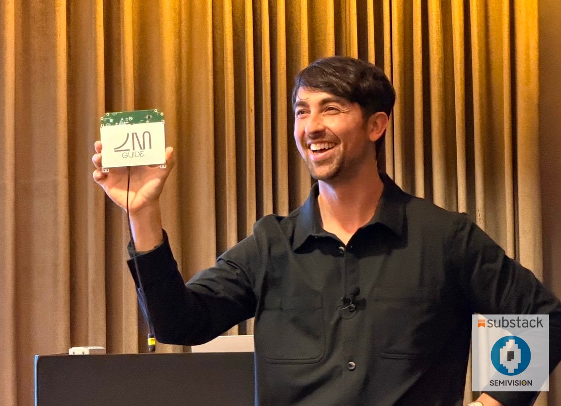
The Guide VLSP platform directly addresses two of the biggest pain points in current co-packaged optics (CPO) architectures: the power wall and bandwidth density bottlenecks.
First, existing CPO systems typically rely on external ELSFP laser modules, which are subject to physical limitations—specifically, connector endfaces can be damaged by heat from contaminants absorbing optical energy, even at power levels of just a few hundred milliwatts. As a result, the total optical power per module cannot be increased beyond a certain threshold, which in turn limits the number of channels or distance a single laser module can support.
The Guide VLSP platform overcomes this by directly fabricating dense laser arrays on silicon substrates and coupling them into photonic chips—eliminating fragile connector interfaces prone to contamination. This design enables the system to safely raise the optical power per fiber to over 100 mW. Higher per-fiber output allows for either longer transmission distances or greater wavelength division multiplexing (WDM) capacity.
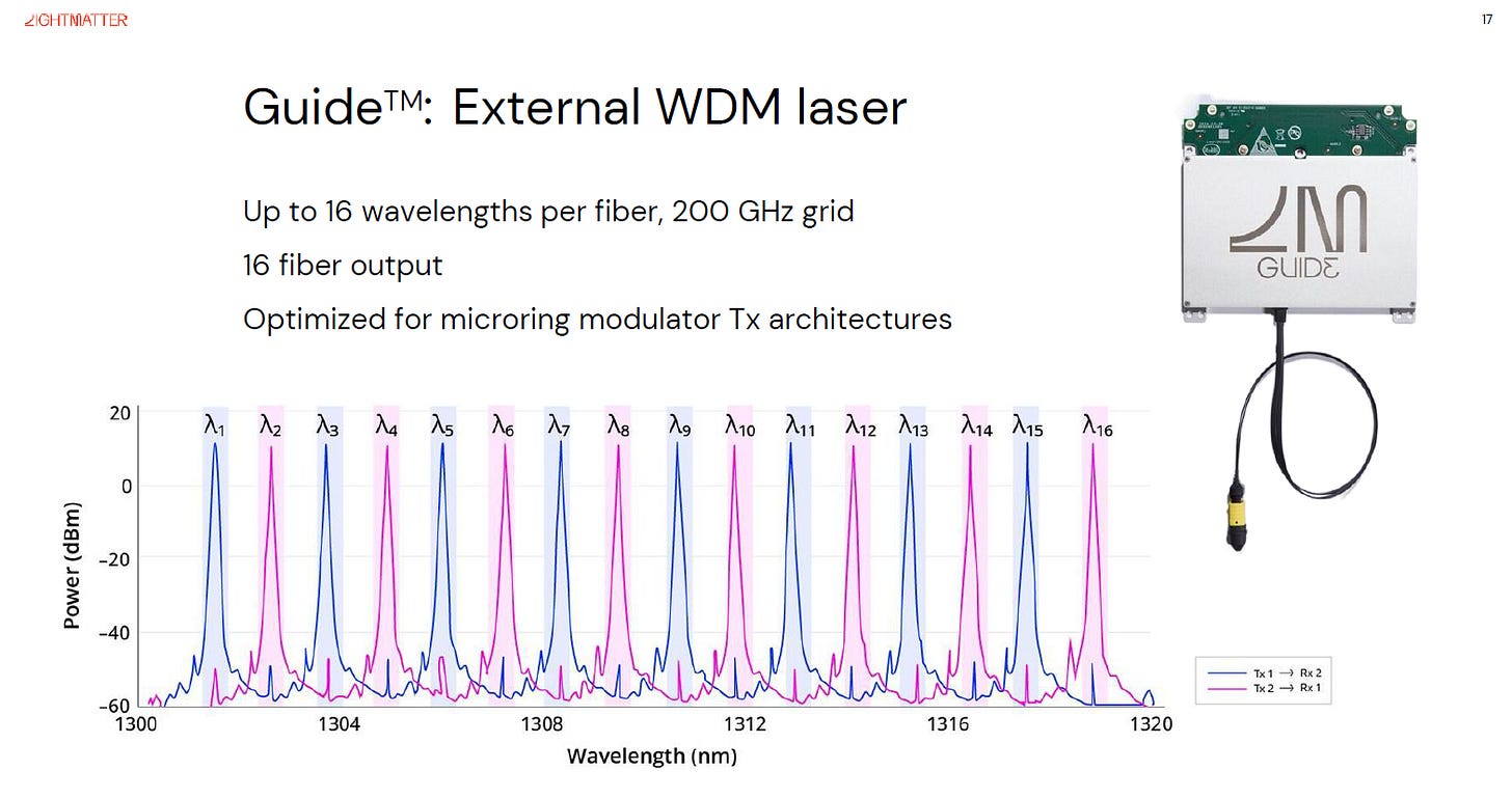
Second, in conventional designs, doubling the total bandwidth of a switch or compute node typically means doubling the number of external laser modules. This leads to linear increases in cost, power consumption, rack space usage, and system complexity. According to Lightmatter, a 51.2 Tbps 800G × 64-port switch would normally require 18 external laser boxes (ELSFPs) occupying roughly 4 rack units (4RU). In contrast, the Guide VLSP solution achieves the same bandwidth using just 2 laser modules, requiring only 1RU and saving 75% of rack space. With an 8× increase in bandwidth density, system complexity and power draw are significantly reduced, breaking the long-standing paradigm that increasing bandwidth necessarily means stacking more optical modules.
Lightmatter Introduces Guide Light Engine for AI, Featuring VLSP Technology
Lightmatter claims VLSP defines a laser roadmap that can scale from a single wavelength to 64 or more, while keeping assembly complexity virtually constant. As they emphasize, “Scalable lasers are the key to realizing true CPO“. Indeed, only when the light source achieves semiconductor-grade scalability and reliability does large-scale optical interconnect become commercially viable. With VLSP, all three pillars of AI infrastructure—compute, interconnect, and light source—have entered the domain of chip-level integration.
In summary, the Guide VLSP platform completes the missing piece in silicon photonics interconnect. Previously, laser sources were kept external to CPO systems—what the industry refers to as “CPO 1.0.” Lightmatter’s approach provides a highly integrated “optical power engine” outside the package, achieving true electro-optical decoupling: compute and optical interconnects are tightly integrated inside the package, while the light generation remains modular and serviceable. This is considered a pragmatic compromise between current engineering constraints and future goals.
Lightmatter Introduces Guide Light Engine for AI, Featuring VLSP Technology
Looking ahead, as VLSP matures and integrates with advanced packaging from TSMC—such as CoWoS-L or COUPE optical integration—we have good reason to expect dramatic gains in power efficiency, bandwidth scalability, and manufacturability for co-packaged optics.
Lightmatter in the Industry Ecosystem: Partnerships and Standards-Driven Momentum
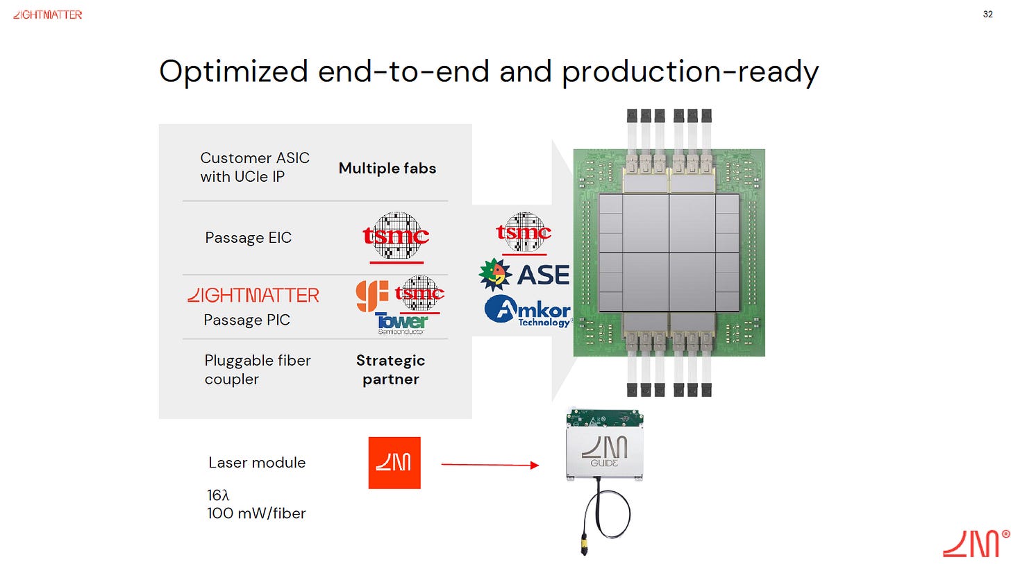
At the forefront of AI infrastructure innovation, Lightmatter recognizes that no single startup can reshape the entire industry landscape alone. To that end, the company is actively forging partnerships across the semiconductor ecosystem—including foundries, packaging providers, IP and EDA vendors, and hyperscale cloud operators—to accelerate the mainstream adoption of silicon photonics.
Lightmatter Test Development
As silicon photonics transitions from research to high-volume manufacturing, test strategy becomes a defining factor in scalability and yield control. Unlike conventional electronic IC flows, photonic devices require a tightly staged validation process that spans pure photonic testing, optical assembly verification, electro-optical validation, and final system-level qualification.
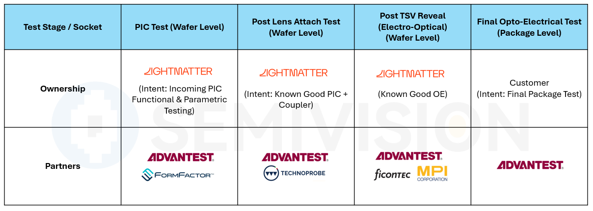
Lightmatter’s test development roadmap reflects this multi-layered complexity. The company adopts a progressive test ownership model, beginning with wafer-level PIC functional screening, advancing through optical coupling and electro-optical validation, and culminating in final package-level opto-electrical testing by the customer. This staged approach not only de-risks integration but also builds a collaborative ecosystem with leading test and photonic assembly partners, forming the foundation for scalable optical engine production in AI infrastructure.

2025年8月10日

2025年4月15日
Semiconductor Manufacturing and ASIC Co-Development

Lightmatter has established close ties with TSMC and its ecosystem partner Global Unichip Corp. (GUC). In 2023, TSMC highlighted optical engines and 3D packaging as core enablers for the AI era during its technology forums and launched initiatives in integrated photonics R&D. GUC—35% owned by TSMC—is a leading ASIC design house with deep expertise in advanced custom chips and packaging. In 2024, Lightmatter and GUC formally announced a strategic partnership to combine Lightmatter’s disruptive Passage photonic interconnect platform with GUC’s ASIC design and packaging know-how, co-developing commercial-grade 3D CPO solutions.
Lightmatter and GUC Partner to Produce Co-Packaged Optics (CPO) Solutions for AI Hyperscalers
Their joint goal: overcome the interconnect bottlenecks limiting AI/HPC scaling, and enable feasible paths for hyperscale data center expansion. Lightmatter CEO Nick Harris remarked, “The world has hit a ceiling on performance-per-silicon. The network is the computer, and that network must be powered by light. GUC’s unparalleled ASIC execution, paired with our photonic interconnects, offers a real escape from the traditional energy-efficiency trap to unlock the massive scalability tomorrow’s AI requires”. GUC emphasized that integrating Passage into its ASIC designs would help address the many complexities of CPO—from architecture, thermals, and mechanics to signal integrity—providing cloud customers with a scalable, energy-efficient platform to accelerate AI deployments.
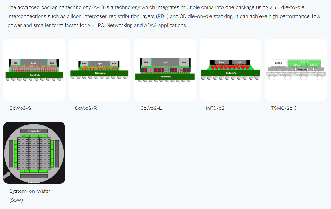
Notably, the collaboration spans the full stack from chip design to advanced packaging: GUC benefits from TSMC’s cutting-edge nodes and 3D integration technologies (such as SoIC), while Lightmatter contributes its silicon photonics IP and system integration expertise. As experts from Taiwan’s ITRI noted, “Optical interconnects are no longer a luxury—they’re essential to sustaining hyperscale AI growth. The GUC-Lightmatter partnership reflects a maturing supply chain and offers a clear blueprint to address the industry’s bandwidth and power challenges”.
Packaging and Manufacturing Partnerships
In packaging and test, Lightmatter has teamed up with ASE Group, the world’s largest OSAT. In late 2024, the two announced plans to co-commercialize the Passage platform by developing the world’s first 3D-stacked photonic engine with pluggable fiber connectivity. ASE is contributing its industry-leading 2.5D/3D heterogeneous integration capabilities—such as Fan-Out and advanced IC packaging—to help realize high-yield assembly of photonic and electronic dies and ensure reliable alignment of high-density fiber arrays. This partnership enables Lightmatter to transform its architectural vision into manufacturable, production-grade products and accelerate mass deployment of high-performance optical engines.

Crucially, ASE also collaborates closely with TSMC in the field of advanced packaging. With this joint effort, Lightmatter positions itself at the nexus of state-of-the-art integration technologies.

2025年6月18日

2025年6月22日
EDA Tools and Interface IP Standardization
Lightmatter has also built partnerships with major EDA and IP providers like Cadence and Synopsys to streamline the design and validation of photonic-electronic co-packaged systems. In early 2026, Lightmatter and Cadence announced a technical collaboration to integrate Cadence’s silicon-proven 112G/224G high-speed SerDes and UCIe die-to-die IP into the Passage optical engine. Cadence also provides its expertise in digital and 3D IC design tools to ensure compatibility with advanced process and packaging nodes. The aim is to deliver a “silicon-validated CPO roadmap” that enables future large-scale AI chiplets and infrastructure deployments.
Lightmatter and Cadence Collaborate to Accelerate Optical Interconnect for AI Infrastructure
The next leap in AI performance demands a fundamental rethinking of data movement. Cadence’s connectivity IP pairs perfectly with our Passage platform. Together we are tackling the toughest challenges in photonic-electronic integration to ensure the next wave of AI clusters reaches their energy and bandwidth goals”. Cadence Silicon Group, added, “As AI workloads scale both vertically and horizontally, infrastructure must evolve. Our partnership with Lightmatter integrates our SerDes and UCIe IP into their new CPO platform, helping customers build scalable, power-efficient AI systems”.
That same week, Lightmatter also announced a partnership with Synopsys via Business Wire, stating it will adopt Synopsys’ 224G SerDes and advanced 3nm UCIe IP into its 3D CPO platform to create scalable, low-latency solutions tailored for future AI infrastructure. These moves clearly show Lightmatter is aligning its photonics stack with industry standards: UCIe-compliant chiplet interfaces, mainstream EDA workflows, and likely future OIF/IEEE optical interconnect protocols. By plugging into the broader ecosystem, Lightmatter’s innovations become easier for customers to adopt and integrate with existing systems—lowering commercial adoption barriers.
End-User Engagement and Ecosystem Advocacy
Lightmatter has also engaged actively with hyperscalers and industry consortia. Major cloud providers like Microsoft and Google, both exploring custom AI infrastructure, have shown strong interest in next-generation interconnects. Lightmatter has reportedly demonstrated sample systems to several of these players and is said to be securing strategic investment and pilot deployment opportunities.

2025年7月25日

2025年6月20日
Additionally, Lightmatter’s engineering team participates in organizations such as the Open Compute Project (OCP) and Optical Internetworking Forum (OIF), contributing to the definition of next-gen CPO interface standards and sharing insights from their work in VLSP and 3D optical packaging to help foster cross-industry consensus.

2025年7月10日
As silicon photonics continues to mature, we are witnessing a historic shift in computing—from transistor-driven scaling to interconnect-driven architectures. As an early mover in this transition, Lightmatter—with its twin platforms, Passage and Guide, and partnerships spanning TSMC/GUC, Cadence, Synopsys, and ASE—is helping unlock the next era of scalable compute. With AI compute demands heading toward the Zetta-scale and data center power nearing gigawatt levels, traditional approaches are rapidly approaching their limits. The silicon photonics path being carved by Lightmatter may well carry us beyond the ceilings of power and bandwidth—ushering in a new era of computation at the speed of light.

2025年6月12日

2025年6月3日
2025年6月2日
2025年6月25日
2025年6月2日
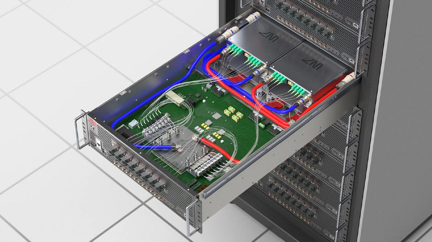
Lightmatter InterConnect Launch Event at OFC 2025
This video also highlights the critical role of silicon photonics and WDM (wavelength division multiplexing) in achieving these advancements and acknowledges the contributions of industry partners like GlobalFoundaries, Amkor Technologies, and ASE Global in bringing these innovations to reality.


PreviousNext
TopLatestDiscussions








See all