IMPACT 2025 Conference Review: Enabling Energy-Efficient AI with Advanced Logic, 3D Packaging, and Photonics
IMPACT 2025 Conference Review: Enabling Energy-Efficient AI with Advanced Logic, 3D Packaging, and Photonics
- Source: SemiVision
- Author: SEMIVISION
- Published: 2026-01-26T14:23:45+08:00
- URL: https://tspasemiconductor.substack.com/p/impact-2025-conference-review-enabling IMPACT 2025 Conference Review: Enabling Energy-Efficient AI with Advanced Logic, 3D Packaging, and Photonics


IMPACT 2025 Conference Review: Enabling Energy-Efficient AI with Advanced Logic, 3D Packaging, and Photonics
Original Article By SemiVision (TSMC, IEEE, VLSI, TPCA, IMPACT)

Jan 26, 2026
∙ Paid
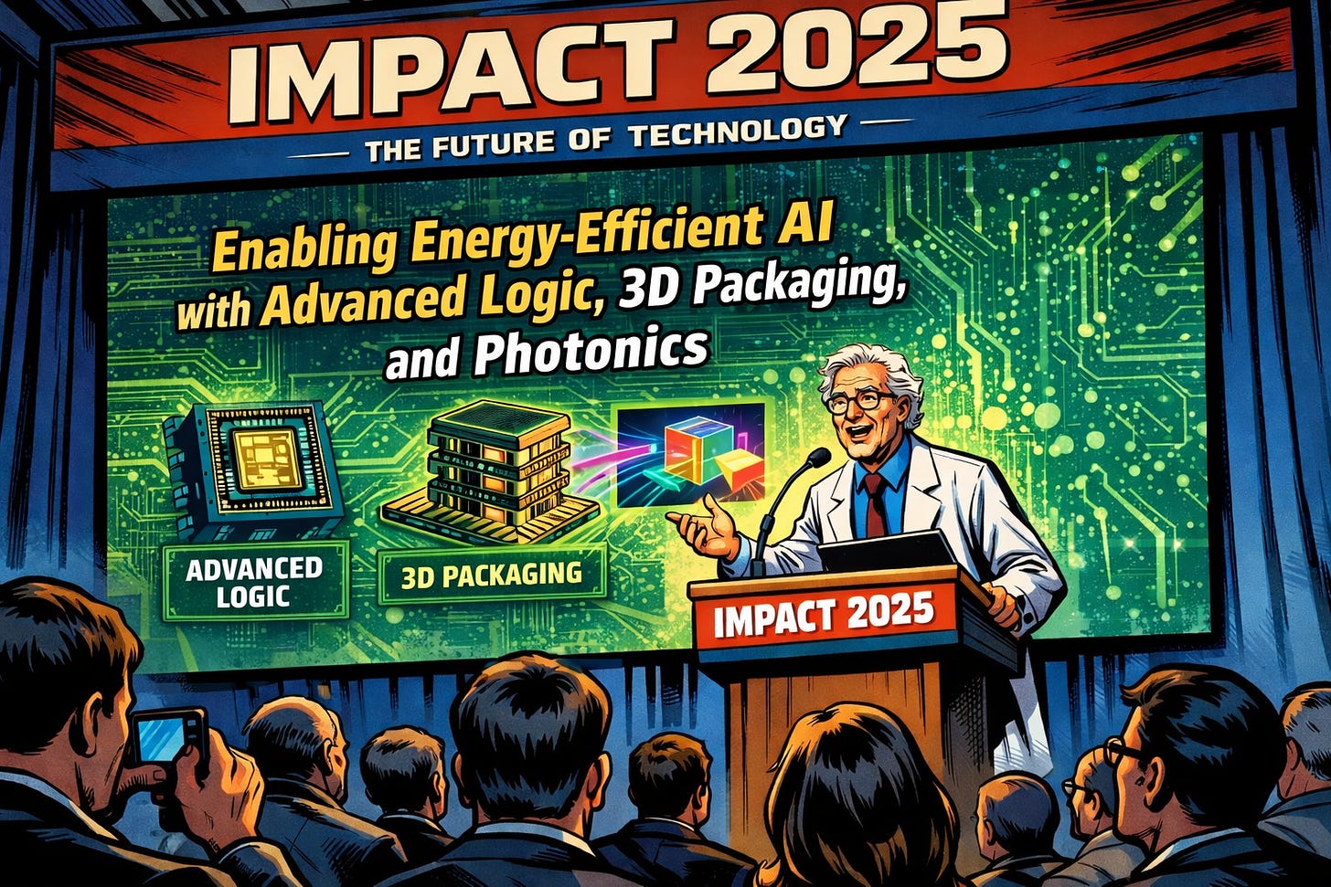
IMPACT 2025 Conference Review: Enabling Energy-Efficient AI with Advanced Logic, 3D Packaging, and Photonics

Since its inception in 2006, the IMPACT Conference has been at the forefront of technological evolution, fostering innovation in the packaging, PCB, and semiconductor industries. Over the past two decades, IMPACT has not only witnessed but actively contributed to rapid advancements in 5G, AI, high-performance computing (HPC), edge computing, and sustainability. Each year, the conference has adapted to the latest trends, driving forward the conversation on emerging technologies and their industrial applications.
Now in its 20th year, IMPACT 2025 embraces the theme “Energy-Efficient AI: From Cloud to Edge,” reflecting the industry’s growing emphasis on high-performance, low-power solutions. As AI applications continue to expand—from data centers to edge devices—the need for advanced PCB, IC substrates, heterogeneous integration, and packaging technologies has become increasingly critical.
This milestone year marks not just a celebration of the past 20 years, but a bold step into the future, where IMPACT continues to lead, inspire, and drive innovation. Join us at IMPACT 2025 as we shape the next era of AI, semiconductor packaging, and PCB technology—powering a smarter, more sustainable world.

2025年10月27日
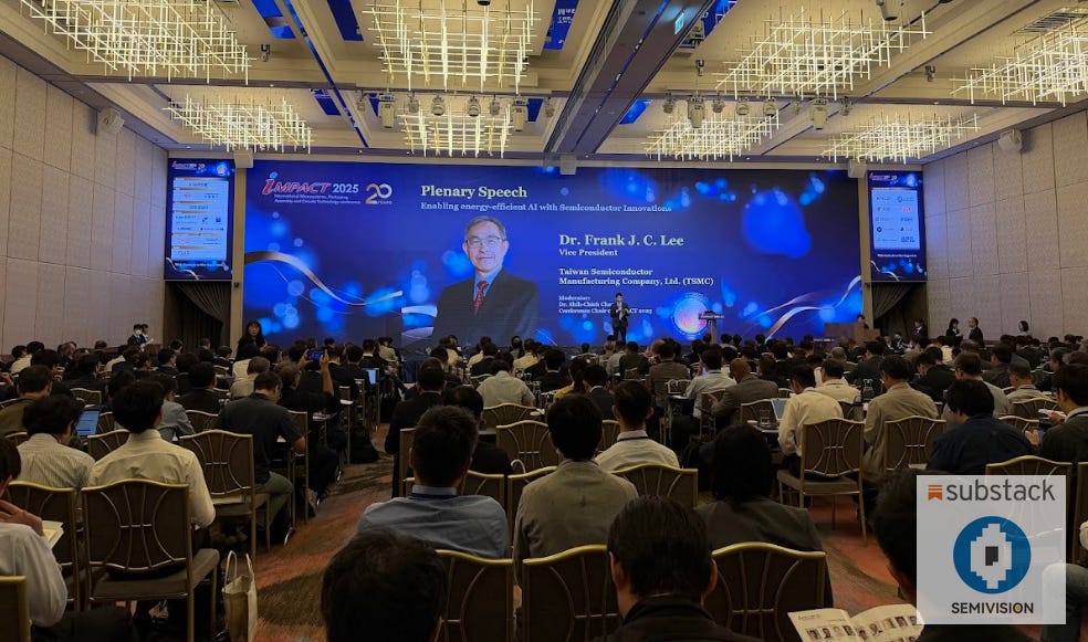
Dr. Frank J. C. Lee, Vice President at TSMC, delivers the plenary “Enabling Energy-Efficient AI with Semiconductor Innovations” at IMPACT 2025. In this comprehensive review, we examine the key insights from TSMC’s presentations atIMPACT 2025– the 20th International Microsystems, Packaging, Assembly and Circuits Technology Conference held in Taipei in October 2025. The central theme of the event, “Energy-Efficient AI: From Cloud to the Edge,” underscores an urgent industry focus on reducing power consumption even as AI compute workloads grow exponentially.

2025年9月25日
2025年6月25日
The plenary talk by Dr. Frank J. C. Lee of TSMC highlighted how AI’s proliferation from hyperscale data centers to edge devices is driving an exponential rise in compute demand and power usage, making energy efficiency a critical bottleneck to further progress. TSMC’s strategy to confront this challenge spans multiple technology domains: advanced silicon logic scaling (from FinFET to nanosheet transistors), 3D packaging and heterogeneous integration techniques, silicon photonics for optical I/O, and new energy-efficient design methodologies. By integrating innovations across process nodes, packaging, and system-level architecture, TSMC aims to dramatically improve performance-per-watt for AI chips and sustain the pace of AI advancements.
2025年5月15日
In summary, TSMC’s presentations at IMPACT 2025 demonstrated a holistic approach to enabling sustainable AI growth. Key announcements included the upcoming 2 nm (N2) semiconductor node with nanosheet transistors slated for volume production in 2025, which continues historical power-performance scaling (delivering ~30% power reduction each generation). Beyond transistor scaling, TSMC detailed breakthroughs in 3D Fabric packaging (chip stacking and chiplet integration), achieving multi-fold energy efficiency gains at the system level. The company also showcased a co-packaged optical engine (COUPE) for silicon photonics, promising an order-of-magnitude reduction in interconnect power. Finally, design-level innovations – from optimized standard cells and memory to AI-assisted EDA tools – are contributing additional efficiency boosts of 5–20% on top of process and packaging improvements. Taken together, these advances reinforce that Moore’s Law is not only alive but augmented by “more-than-Moore” approaches, paving the way for the next era of energy-efficient AI computing.
Major Themes and Technical Innovations
The presentations at IMPACT 2025 centered on several major themes and technical innovations aimed at energy-efficient AI. Below we summarize the primary focus areas that emerged, each of which will be examined in detail in subsequent sections:
Exponential AI Compute Growth vs. Power Limits:AI models and applications are expanding from cloud to edge, driving massive increases in compute requirements (100× or more) and causing power demand to skyrocket. This trend threatens to outpace traditional technology scaling, making efficiency improvements urgent.
Advanced Logic Scaling (FinFET to Nanosheet):TSMC is transitioning its transistor architecture from FinFET to Gate-All-Around nanosheet devices at 2 nm, alongside other node innovations like backside power delivery. These advances continue to provide ~15–30%per-generationpower savings and performance gains, which are critical for AI chips.
3D Packaging and Heterogeneous Integration:TSMC’s 3DFabric platform encompasses 2.5D and 3D packaging technologies (CoWoS®, InFO®, SoIC®, etc.) that integrate multiple chips and memory in one package. By shortening communication distances and enabling larger composite dies, these techniques offer significant system-level energy efficiency gains (e.g. 6.7× better power efficiency moving from 2.5D to 3D stacking).
Silicon Photonics for Optical I/O:To overcome electrical I/O power bottlenecks, TSMC is developing co-packaged optical engines (the COUPE architecture) that integrate photonics with silicon. Optical interconnects can reduce per-bit energy by an order of magnitude (5–10× improvement) and cut latency 10–20× versus traditional pluggable optics.
Energy-Efficient Design and EDA:Beyond hardware, TSMC highlighted design-technology co-optimization and AI-assisted design as key to squeezing extra efficiency. This includes new standard cell designs (e.g. optimized flip-flops), dynamic voltage SRAM, compute-in-memory accelerators, and using AI tools for chip layout – collectively yielding additional 5–20% power reductions and productivity gains in chip design.
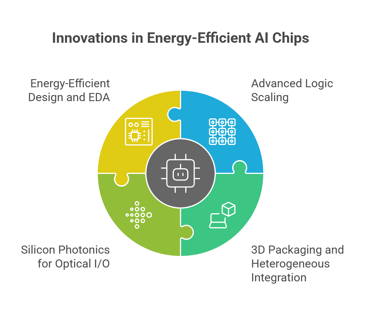
In the following sections, we delve into each of these areas, drawing on data and slides from the conference to illustrate TSMC’s innovations. The goal is to provide a detailed technical analysis of how TSMC is addressing the power-performance challenge for AI, and what these developments mean for the semiconductor industry going forward.
TPCA: IMPACT 2025|A Record-Breaking Milestone!
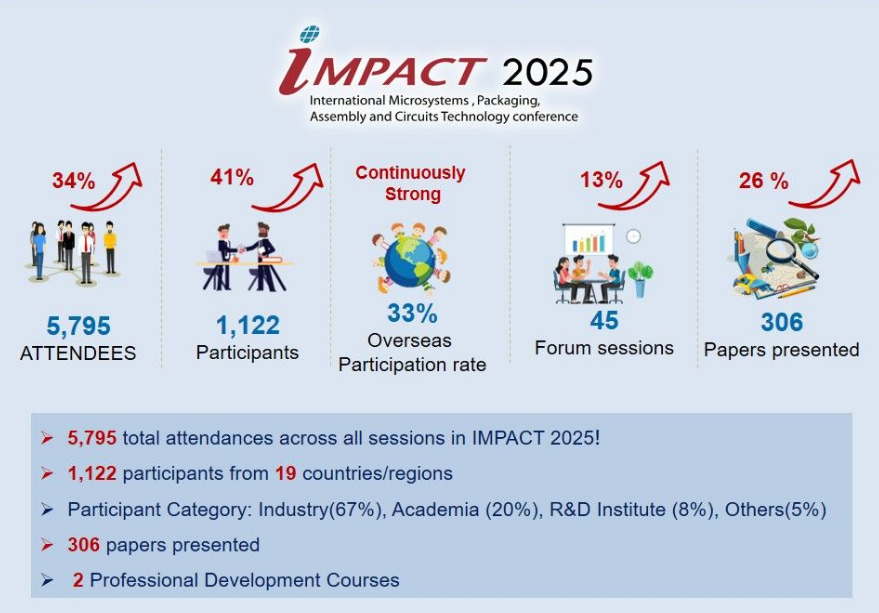
TPCA: This year, IMPACT 2025 reached 5,795 total attendances and 1,122 registrations — both marking our highest record in history! We sincerely thank all our speakers, sponsors, participants, and committee members for your incredible support and contribution.
Together, we have made this 20th-anniversary edition truly remarkable
Thank you for making IMPACT 2025 a record-breaking success!
Your participation and enthusiasm continue to drive innovation, collaboration, and growth across the global electronics community.
IMPACT 2026 will return on October 19–22, 2026 — we can’t wait to see you again for another inspiring year of innovation and ideas!
For Paid Member, SemiVision will discuss topics on
AI Computing Trends and Power Demand
Advanced Logic Innovations: From FinFET to Nanosheet (2 nm and Beyond)
Energy-Efficient Design Techniques (DTCO, Standard Cells, and AI-Assisted EDA)
3D Packaging Technologies and Heterogeneous Integration
SemiVision Tech Insight Report
Looking ahead to 2026, SemiVision will officially launch a new suite of enterprise-level customized services, with core clients focused on Business Development and Market Intelligence teams. These services are designed to help companies navigate the semiconductor industry’s rapid transformation by gaining timely access to decision-grade technology and market intelligence. Rather than simply aggregating information, SemiVision operates through a project-based approach, delivering in-depth, tailored analysis around clients’ priority topics — including technology node evolution, shifting supply-chain roles, competitive landscape restructuring, and emerging commercial opportunities.
SemiVision’s 2026 customized services will center on key areas such as advanced packaging (CoWoS / CoPoS / SoIC / CPO), silicon photonics and Optical I/O, AI and HPC system architecture, bottleneck migration in critical materials and equipment, and the real supply-chain impact of geopolitics and capacity allocation. Through cross-technology and cross-value-chain analysis — integrating process feasibility, production timelines, cost structures, and customer adoption cycles — we support BD and MI teams in identifying which technologies are approaching inflection points, which supplier roles are rising or being displaced, and how complex industry changes can be translated into insights usable for internal decision-making and external strategic communication.
For readers seeking deeper insight into the structural evolution of the semiconductor industry, SemiVision has long focused on the most critical — yet often oversimplified — core issues. These include advanced and mature node evolution, bottleneck migration in key materials and equipment, competitive–cooperative supply-chain dynamics, and the substantive trade-offs between different technology paths. Beyond organizing public information, we conduct cross-analysis from the perspectives of process feasibility, mass-production barriers, cost structures, customer adoption timing, and long-term competitiveness — helping readers understand why the industry is moving in certain directions and where it may head next. For those requiring more advanced, research-depth industry analysis or customized discussions (such as the technology positioning of specific companies, supply-chain roles, or mid-to-long-term trend assessments), we welcome you to contact us via email for further exchange.:jett@semivisiontw.com、eddyt@semivisiontw.com
SemiVision Tech Insight Report Topics
Advanced Packaging Technology Roadmap and Materials Evolution
Silicon Photonics Platform and Materials Development Trends
Thermal Management Materials for High-Performance Computing and AI Systems
Interposer Architecture and Materials Innovation
Hybrid Bonding Processes and Materials Integration
Through-Glass Via (TGV) Technology and Glass Substrate Development
Key Takeaways from Major Semiconductor Technical Forums
Metalens and Metasurface Optics Materials Evolution
IC Substrate Materials, Process Technology, and Supply Chain Analysis

2025年12月31日
AI Computing Trends and Power Demand

Source: microsoft
“AI Everywhere” – Ubiquitous Deployment:One overarching theme is that AI workloads are no longer confined to cloud data centers; they are rapidly proliferating into edge devices and everyday electronics. In his keynote, Dr. Lee emphasized that the AI revolution is permeating all levels of computing, from hyperscale servers to smartphones, IoT sensors, VR/AR headsets, autonomous vehicles, and even robots. This ubiquity is enabling new applications but also dramatically increasing aggregate compute demand and power consumption. Figure 1 shows a conceptual map of AI’s reach – spanning data centers and various intelligent devices – underscoring that “AI is infused into every device to enable new applications”. As AI becomes truly everywhere, the industry faces the challenge of powering these capabilities efficiently.
Exponential Growth of AI Model Computation:The compute requirements of state-of-the-art AI models have been growing exponentially with each breakthrough. TSMC presented data highlighting how training FLOPs for leading AI models have increased by orders of magnitude from 2017 to 2023. From early breakthroughs like AlphaGo Master (2016) to modern large language models like GPT-3 (2020) and beyond. The trend is clear – each generation (e.g., GPT-4 and upcoming multimodal or “agentic” AI systems) demands vastly more computation than its predecessor. The graph indicates training complexity on the order of10^24 – 10^25 FLOPsfor 2023-era models, nearly 100× higher than the compute used by late-2010s models. This growth is driven by larger model sizes, more sophisticated algorithms (such as chain-of-thought reasoning and multi-step inference), and the integration of multiple data modalities.

At the same time,inference workloadsare becoming heavier. TSMC noted that traditional “one-shot” inference (a single forward pass) is giving way to more complex inference techniques. For example,iterative reasoning or chain-of-thought inferencefor AI assistants can require ~10× the compute of a one-shot inference, and emergingagentic AI(autonomous AI agents that plan and act) might need100×the compute per task of simple inference . In short, both training and inference are on trajectories ofexplosive growthin computational intensity.

Surging Power Demands for AI Hardware:This unprecedented growth in AI compute directly translates tosoaring power consumptionin AI hardware. More complex models not only require more operations, but also often run on specialized accelerators (GPUs, TPUs, AI ASICs) deployed at scale. TSMC provided striking statistics: over the past five years, the power budget of high-end AI accelerator packages has more than tripled. In 2020, a typical flagship AI training chip might have had a thermal design power on the order of 300W; by 2025, top AI accelerators (leveraging bigger silicon interposers and multi-die integration) exceed>900W per package. This >3× increase in power per chip is illustrated inFigure 3(left), which charts the progression from earlier 2.5D packages (e.g., TSMC’s CoWoS-S) to newerCoWoS-L/SoICheterogeneous integrations that allow much larger effective die sizes and power envelopes.

Simultaneously, thevolume of AI chips deployedhas skyrocketed. Data center operators are installing AI accelerators in unprecedented quantities to meet demand in cloud AI services. According to TSMC’s estimates, the number of AI accelerator units deployed globally grew 8× in just three years, roughly from 2023 to 2026. picuture below shows a bar chart of this trend, with TSMC projecting continued steep growth. This combination – more power-hungry chips, multiplied by many more deployments – creates a compounding effect on total power consumption. It’s no surprise that TSMC’s keynote stressed energy efficiency as “paramount for sustainable AI growth”, as the industry cannot simply continue on this trajectory without hitting energy and cooling limits.

Units deployed – The volume of AI accelerator chips installed in data centers is exploding, with an ~8× increase from 2023 to 2026. This reflects the proliferation of AI workloads in industry. The product of these trends is a dramatic surge in total power consumption, underscoring the urgent need for efficiency improvements.
Implications:These observations set the stage for why TSMC and the semiconductor industry are urgently focusing on energy efficiency. AI’s exponential compute appetite is on a collision course with practical power and cooling limits. As noted in the presentation, energy efficiency is now the key factor determining sustainable AI progress. Without major improvements in performance-per-watt, AI growth would be constrained by power costs and environmental impact. The next sections review how TSMC is addressing this challenge via cutting-edge logic technology, advanced packaging, photonic integration, and co-optimization at the design level.
Advanced Logic Innovations: From FinFET to Nanosheet (2 nm and Beyond)
One pillar of TSMC’s strategy is continued innovation in semiconductor logic technology – i.e., new transistor architectures and process nodes that deliver better performance and energy efficiency. At IMPACT 2025, TSMC reaffirmed its process roadmap for the next several years, highlighting the transition from FinFET transistors (used from 16 nm through 3 nm generations) to nanosheet (gate-all-around) transistors in the upcoming 2 nm node. This marks a major device architecture change aimed at sustaining transistor scaling gains.

TSMC advanced logic roadmap, showing the evolution from FinFET-based nodes (N5, N4, N3 families) to nanosheet gate-all-around nodes (N2 and successors). N2 in 2025 will be TSMC’s first GAA transistor technology, followed by enhanced versions (N2P, N2X) and nodes featuring backside power delivery (denoted as “A16” withSPR, an upcoming 2026 node). Continuous improvements to N3/N5 nodes (N3E, N4P, etc.) run in parallel to add value. This roadmap underscores TSMC’s commitment to regular logic scaling as a foundation for energy-efficient AI.
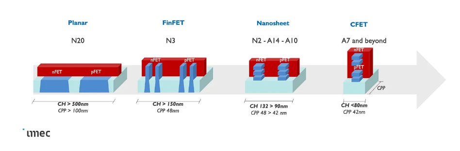
2 nm and Nanosheet Transistors:TSMC announced that its first 2 nm (N2) technology will enter volume production in the second half of 2025, making it one of the world’s earliest high-volume nodes with gate-all-around (GAA) transistors. Unlike FinFETs (which have a fin-shaped 3D channel), the GAA “nanosheet” device wraps the gate fully around stacked horizontal nanosheet channels, providing superior electrostatic control. This enables further transistor scaling to improve efficiency. According to TSMC, N2’s initial version focuses on mobile and high-performance computing, and an optimized variant N2P will follow about a year later (likely 2026).
Backside Power Delivery (A16 node):Beyond N2, TSMC is preparing a node referred to as A16 (planned for ~2026–27) which will introduce backside power delivery – indicated as “SPR” (possiblyStacked Power Rail) in the roadmap (Fig. 4). Backside power, also known as buried power rails or PowerVia in Intel’s terminology, involves routing power lines on a separate wafer side or layer, freeing up the front side for signal routing and reducing IR drop. TSMC expects A16’s backside power implementation to yield an additional 8–10% speed gain or 15–20% power reduction compared to conventional interconnect at N2P. This is significant as it attacks resistive losses in power distribution, a growing issue at advanced nodes. A16 will target AI and HPC chips with very high power densities, where backside power can especially improve efficiency.
3D Packaging Technologies and Heterogeneous Integration

Beyond on-chip transistor improvements, TSMC underscored that advanced packaging and heterogeneous integration are now key to improving system-level energy efficiency for AI hardware. Under the umbrella of TSMC 3DFabric (the company’s family of 2.5D and 3D integration technologies), several packaging innovations were highlighted at IMPACT 2025. These allow multiple dies (logic, memory, chiplets) to be integrated in one package with high-bandwidth, power-efficient connections, effectively extending Moore’s Law in the third dimension.
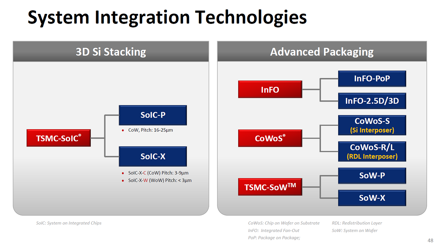
TSMC’s 3DFabric advanced packaging portfolio: The 3DFabric platform encompasses 3D chip stacking (TSMC-SoIC®) where dies are bonded directly, as well as 2.5D advanced packaging like InFO (Integrated Fan-Out) and CoWoS (Chip-on-Wafer-on-Substrate), and the emerging SoW (System on Wafer) approach for wafer-scale integration. By combining these technologies, TSMC enables heterogeneous integration of logic + memory + analog etc., with much higher interconnect density and lower power per bit than traditional PCB-level integration. These packaging innovations are credited with significant energy efficiency gains at the system level.
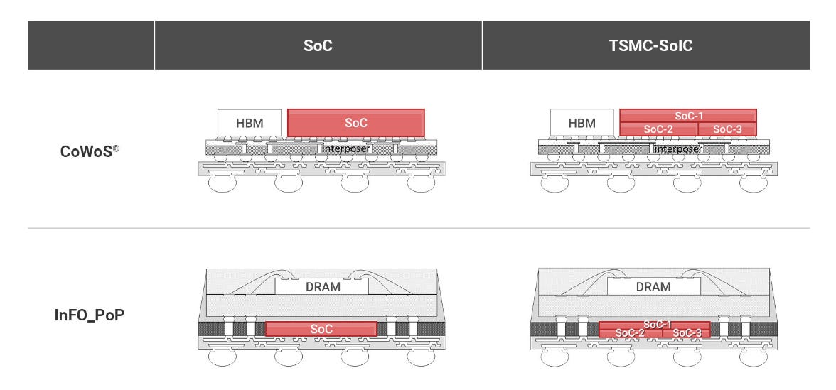
2.5D to 3D Integration – Energy Efficiency Gains:One of the striking data points TSMC shared is the efficiency improvement when moving from a 2.5D interposer integration to a true 3D stacked integration. In a 2.5D package like CoWoS (where multiple chiplets sit side by side on a silicon interposer), reducing the interconnect pitch can improve power efficiency of chip-to-chip communication. For example, TSMC noted that going from a 45 µm microbump pitch to 25 µm on CoWoS (a refinement of their interposer tech) yields about a 1.6× improvement in energy efficiency for those links. This is because shorter, denser connections have less capacitance and require less drive power per bit.

Source: SK Hynix
Taking it a step further, TSMC’s SoIC (System on Integrated Chips) technology enables3D stacking, where dies are bonded directly face-to-face or face-to-back without an interposer, using through-silicon vias (TSVs) or hybrid bonding. TSMC reported that a 3D SoIC integration can achieve ~6.7× the energy efficiency of a comparable 2.5D solution. This dramatic gain comes from the orders-of-magnitude increase in interconnect density and reduction in length that 3D stacking provides – essentially, power-hungry off-chip or interposer links can be replaced with tiny vertical connections consuming far less energy. The trade-off is that 3D stacking currently limits the overall package size (a stacked assembly might be limited to one reticle size per die, vs. a large interposer can tile multiple reticles). TSMC acknowledged this, noting the“smaller integration area (1× reticle vs 9.5×)”for 3D vs 2.5D. In practice, this means extremely large AI systems (like >600 mm² of silicon) might still need 2.5D interposers, but wherever feasible, 3D stacking will give better energy efficiency for the integrated system.
To support multi-die architectures, TSMC and partners are developing die-to-die (D2D) interface IP that complies with the emerging UCIe (Universal Chiplet Interconnect Express) standard. This was mentioned as being available from IP providers like Alphawave and Synopsys. Such standardized chiplet interfaces ensure that companies can mix and match dies (potentially even from different vendors or fabs) in TSMC’s advanced packages, broadening the use of 2.5D/3D integration.
Memory Integration – HBM Improvements:High Bandwidth Memory (HBM) is a crucial component for AI accelerators, and TSMC is optimizing how HBM stacks interface with logic dies. Traditionally, HBM DRAM stacks sit on an interposer or substrate and connect to the GPU/AI chip through thousands of microbumps. TSMC discussed moving the HBM interface onto a logic base die. In particular, the upcoming HBM4 generation was highlighted: by placing HBM4 on a TSMC N12 process base (instead of a conventional DRAM base), they achieved 1.5× the bandwidth and energy efficiency over HBM3e. Furthermore, TSMC is developing custom HBM base dies in N3P process, which will allow lowering the IO voltage from ~1.1 V to ~0.75 V, bringing additional power savings. Essentially, by leveraging advanced logic processes for memory interface circuitry, TSMC can run the HBM at lower power per bit while increasing data rates – a boon for AI chips that often use 4–8 HBM stacks. This approach blurs the line between “logic” and “memory” technologies, again an example of heterogeneous integration for efficiency.

At the 2025 OIP Ecosystem Forum, TSMC revealed two major architectural shifts that will fundamentally reshape how next-generation AI memory stacks are built. These changes center on the base die—the silicon layer beneath HBM that hosts the PHY, logic circuits, and increasingly, the memory controller itself.
- HBM4: Base Die Migrates to TSMC N12
TSMC confirmed that HBM4 will abandon the traditional DRAM-process base die used in HBM3E and earlier generations. Instead, the base die will now be manufactured on TSMC’s N12 logic process, enabling:
Operating voltage reductionfrom1.1V → 0.8V
Higher bandwidththanks to denser, faster logic
Significant improvement in base-die power efficiency
For the first time, the base die is no longer a legacy DRAM artifact—it becomes a true logic platform. This shift mirrors the broader industry trend of treating memory not as a passive component, but as an active, tightly integrated compute partner.
- C-HBM4E: Logic + Memory Controller on N3P
TSMC’s second announcement takes integration further: the base die for C-HBM4E will move again to TSMC N3P, incorporating both the logic functions and the memory controller (MC) directly into the silicon.
Benefits include:
Voltage reduction to 0.75V
Even higher power efficiency vs. N12
Memory controller co-located with the base die
Reduced signaling distance between logic and DRAM stacks
This architecture places intelligence physically closer to the memory layers, minimizing I/O loss, reducing latency, and improving power efficiency—an essential requirement as AI workloads scale toward trillion-parameter models.
Memory has become the limiting factor in AI computing. As GPUs evolve into multi-chiplet architectures and accelerators require tens of terabytes per second of bandwidth, traditional HBM designs cannot keep up. TSMC’s HBM4 and C-HBM4E roadmaps recognize this:
AI accelerators increasingly rely on logic-enhanced memory subsystems.
HBM becomes less of a DRAM stack and more of a compute-adjacent subsystem.
Power efficiency becomes the decisive metric for full-rack AI systems.
TSMC’s customized N12 and N3P base dies effectively push the memory subsystem closer to becoming a “near-memory compute platform”—a stepping stone toward future memory-centric AI architectures.
SemiVision Insight
TSMC’s data shows nearly 2× base-die power efficiency improvement as the platform progresses from HBM3E → HBM4 → C-HBM4E. This advantage compounds across a full AI rack, where hundreds of HBM stacks operate simultaneously. For hyperscalers, shaving even a few watts per stack translates into major efficiency gains at datacenter scale.
The move also underscores a broader industry reconfiguration:
TSMC is no longer just enabling chip makers—it is now shaping memory architectures themselves.
This marks a turning point for the entire HBM ecosystem, influencing DRAM vendors, logic designers, module integrators, and system architects worldwide.

2025年6月2日
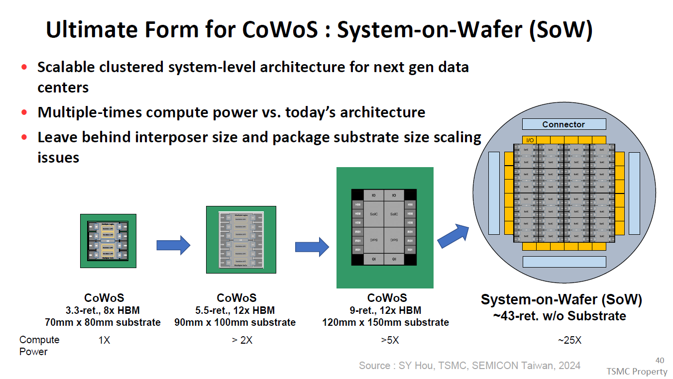
System on Wafer (SoW):TSMC briefly alluded to SoW, which stands for System on Wafer, as part of 3DFabric. SoW is a wafer-level integration scheme where many chiplets are embedded in or bonded to a common wafer, effectively creating a large, wafer-scale subsystem. This could be used for wafer-scale AI engines or very large interposer-like constructs. While details were sparse at the conference, the inclusion of SoW suggests TSMC is exploring even more ambitious integration for HPC – potentially enabling massive AI systems that approach wafer-scale computing (with obvious implications for performance and power if done effectively).
Power Delivery and Decoupling in Packaging:As packages deliver more power to chips (recall >800W in some AI accelerators), managing power integrity in the package becomes critical. TSMC mentioned innovations in decoupling capacitance on package substrates, such as Ultra-High-Performance MIM capacitors and Embedded Deep Trench Capacitors (EDTC), which together can increase power delivery efficiency and stability. They claim these can enable 1.5× higher power density delivery without integrity loss. Moreover, AI-driven tools are helping automate the placement of these capacitors and the complex mesh routing on advanced packages – with reported productivity boosts of 10× to 100× in certain substrate design tasks. While esoteric, these details highlight the depth of co-design required at the package level to support energy-hungry AI chips.
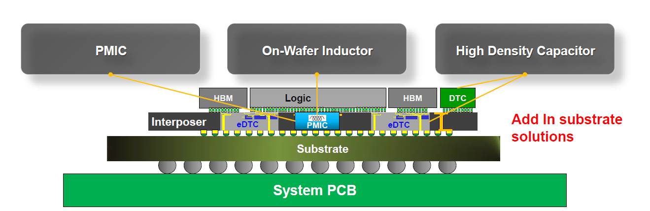
Source: TSMC
Overall, TSMC’s packaging advances reinforce a paradigm shift: performance scaling now heavily depends on “beyond-Moore” integration (multiple dies, 3D stacking, advanced memory integration) as much as on shrinking transistors. By dramatically reducing the energy per bit for chip-to-chip communication and enabling larger effective dies, 3DFabric technologies directly address the bandwidth and power bottlenecks in modern AI systems. For instance, a 6.7× efficiency gain from 3D integration means an AI accelerator module that might have consumed, say, 1000 W to achieve a certain throughput with 2.5D could potentially deliver the same throughput for ~150 W using 3D stacking (all else equal). These are transformative improvements.
Silicon Photonics and Optical Interconnects
The final major technology pillar highlighted by TSMC for enabling energy-efficient AI is the adoption of silicon photonics for data communication. As chips and systems scale, off-chip communication (whether between chips in a server or between servers in a datacenter) becomes a significant portion of the total power. Traditional electrical interconnects (copper traces and wires) consume a lot of energy, especially at high bandwidths over long distances, and they add latency. Co-packaged optics – integrating optical transceivers closely with switch/processor silicon – is seen as a promising solution. TSMC’s contribution is in providing the technology platform (photonics + electronics integration) to make this happen.

2025年6月22日
At IMPACT 2025, TSMC described a COUPE optical engine architecture, which stands for a vertically stacked Electronic-Integrated-Circuit + Photonic-Integrated-Circuit engine. In essence, they can bond or integrate a photonics die (with modulators, photodetectors, waveguides made in something like silicon photonics process) atop or beside a CMOS die that contains the electrical circuits (lasers drivers, amplifiers, SerDes, etc.). By doing so within the package, the optical transceiver is “co-packaged” with the main logic (for example, an AI accelerator or a network switch ASIC).
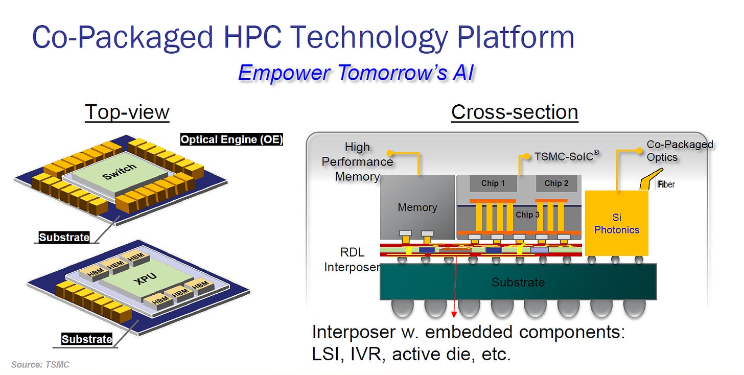
The benefits, as quantified by TSMC, are impressive: a co-packaged optics solution can offer about 5–10× better power efficiency (pJ/bit) and 10–20× lower latency compared to a conventional pluggable optical module in the network rack. By comparing different levels of optical integration:
A standard pluggable optics module (optical engine on the PCB, inches away from the chip) might have an efficiency >30 pJ/bit and is limited by the need to drive off-package signals, adding latency.
Moving the optical engine onto the package substrate (closer to the chip) can reduce energy to ~10 pJ/bit and improve latency somewhat.
Integrating the optical engine on a high-density silicon interposer or alongside the chip (co-packaged) brings it down to ~5 pJ/bit or less, with perhaps one-tenth the latency of pluggables.
A future scenario of optical interfaces directly on an interposer adjacent to processor cores could push energy <2 pJ/bit and latencies to a few tens of nanoseconds (virtually eliminating the penalty of chip-to-chip communication).
2025年6月2日
Silicon Photonics Co-Packaged Optics (COUPE) vs. traditional interconnect: By integrating optical transceivers within the package (or on the interposer) of an AI accelerator or switch, TSMC’s COUPE approach can achieve 5–10× lower energy per bit and 10–20× lower latency compared to pluggable optical modules. The diagram compares a typical copper link (~30 pJ/bit) and pluggable optics (~10+ pJ/bit) versus co-packaged optics on substrate (~5 pJ/bit) and on interposer (~2 pJ/bit). Co-packaged silicon photonics thus dramatically improves I/O efficiency, which is critical as bandwidth demands between chips soar.

This push for optical I/O is aligned with industry trends: as AI systems scale, the amount of data that needs to be shuffled (between processors, and between processors and storage or network) is huge. Electrical I/O at tens of terabits per second would burn too much power and generate too much heat. By moving to optical, which has lower signal attenuation and can potentially multiplex more data per link, the power can be reduced greatly.
TSMC’s role is enabling the integration of the photonics with minimal added cost. The COUPE engine implies they’ve developed ways to bond photonic dies (perhaps made in a silicon photonics process) with high alignment accuracy to their package or interposer. They mention “vertically stacked EIC + PIC”, indicating perhaps a die stacking where the electronic IC is beneath and the photonic IC on top, connected by fine-pitch bonds. This could even leverage technologies like SoIC (3D chip stacking) adapted for photonic dies. The result is an integrated optical engine within the same package as the main chip, eliminating the long PCB traces and extra optics modules.
By quantifying 5–10× efficiency gains and 10–20× latency reduction, TSMC gave a clear message: optical I/O is likely to become part of the standard toolkit for high-end chips (like AI accelerators and switches) in coming generations. For example, a future AI training system might have co-packaged optical fibers coming directly out of the GPU packages to connect to other nodes or to an optical network, instead of using traditional electrical cables or backplanes. This can save significant power at the cluster level.
Additionally, TSMC noted that these photonics advances are being enhanced via co-design with EDA companies: they cited Synopsys and Ansys co-optimizing the photonic-electronic codesign yielding another ~1.2× efficiency improvement. This indicates that the design tools for integrating photonics (handling the thermal, signal integrity, and optical routing challenges) are maturing in TSMC’s ecosystem.

In summary, silicon photonics at TSMC is aimed at revamping data communication for AI systems. It tackles one of the biggest contributors to energy per operation, which is data movement. By cutting I/O power by an order of magnitude, even as throughput needs increase, optical integration will help ensure that scaling out AI clusters doesn’t hit an interconnect power wall. This is especially relevant for edge vs cloud considerations too: for edge devices, photonics might be less immediately applicable, but for cloud data centers and HPC, it’s game-changing. And as edge devices often connect to the cloud, ultimately the power efficiency of those links matters for the whole system’s efficiency.
TSMC’s involvement here also signifies how foundries are extending their value proposition beyond just making chips to helping assemble entire systems. Packaging and now photonics are part of their offerings. This trend might shape how customers design AI systems – potentially preferring a one-stop solution where TSMC provides the logic, packaging, and integrated photonics, rather than sourcing optics separately.

2025年6月12日


PreviousNext
TopLatestDiscussions








See all