Co-Creating the Future of Integrated Photonics: Insights from Netherlands–Taiwan Collaboration
Co-Creating the Future of Integrated Photonics: Insights from Netherlands–Taiwan Collaboration
- Source: SemiVision
- Author: SEMIVISION
- Published: 2026-01-13T09:38:27+08:00
- URL: https://tspasemiconductor.substack.com/p/co-creating-the-future-of-integrated Co-Creating the Future of Integrated Photonics: Insights from Netherlands–Taiwan Collaboration


Co-Creating the Future of Integrated Photonics: Insights from Netherlands–Taiwan Collaboration
Original Article by SemiVision

Jan 13, 2026
∙ Paid

In November 2025, SemiVision collaborated with the Netherlands Office in Taipei (NLOT) as part of the Taiwan Delegation to the Netherlands, joining the visit to Eindhoven forPIC Summit Europe. As a participant in the delegation, SemiVision will actively support event promotion, on-site activity coverage, and post-event documentation, delivering structured event reports, ecosystem mapping, and in-depth industry analysis white papers focused on integrated photonics and next-generation semiconductor technologies.

2025年10月24日

2025年11月12日
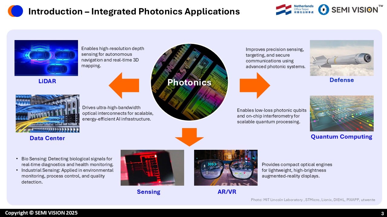
Integrated Photonics Applications: From Infrastructure to Intelligence
Integrated photonics is no longer a niche technology confined to academic laboratories or experimental optical components. It is rapidly becoming a foundational platform technology, reshaping how data is generated, transmitted, sensed, and processed across a wide range of industries. Much like CMOS scaling once redefined electronics, integrated photonics is now redefining the physical limits of bandwidth, latency, power efficiency, and sensing precision.
At its core, integrated photonics integrates optical components—such as waveguides, modulators, detectors, and light sources—onto a single chip or tightly coupled module. By replacing or augmenting electrical signal paths with optical ones, photonics enables orders-of-magnitude improvements in data throughput and energy efficiency, while also unlocking entirely new sensing and computing paradigms.
This article explores the major application domains driving integrated photonics adoption today, and explains why photonics is increasingly viewed as a system-level enabler rather than a discrete component technology.
Unlike traditional optics, which rely on discrete lenses, fibers, and bulk components, integrated photonics leverages semiconductor-style fabrication to deliver scalability, repeatability, and co-integration with electronics. This allows photonic systems to move closer to compute, memory, and sensors—minimizing signal loss and latency while improving reliability.
Crucially, photonics is not replacing electronics; it is complementing and extending them. As electrical interconnects approach fundamental limits in speed and power density, photonics offers an alternative physical domain for information transfer and sensing. This convergence is now visible across multiple sectors.
Data Centers: Breaking the Bandwidth–Power Wall
The most immediate and commercially mature application of integrated photonics is in data centers and AI infrastructure.
Modern AI workloads demand massive data movement between GPUs, accelerators, memory, and storage. Electrical interconnects, however, suffer from rising power consumption, signal integrity issues, and limited reach as speeds scale beyond 112G and toward 224G per lane.
Integrated photonics addresses this challenge by enabling ultra-high-bandwidth optical interconnects that deliver:
Higher data rates over longer distances
Lower power per bit
Reduced thermal burden compared to copper-based solutions
As AI clusters scale from racks to rows to entire data halls, photonics becomes essential for maintaining performance without unsustainable energy growth. This is why silicon photonics is now a strategic technology for hyperscalers, networking vendors, and AI platform providers.
Looking forward, the industry is moving from pluggable optics toward co-packaged optics (CPO), where optical engines are placed in close proximity to compute dies. This transition further elevates photonics from a peripheral module to a core system architecture element.
LiDAR and Autonomous Systems: Seeing with Light
Another major growth area for integrated photonics is LiDAR (Light Detection and Ranging), particularly for autonomous vehicles, robotics, and smart infrastructure.
LiDAR systems rely on precise optical emission, steering, and detection to construct high-resolution 3D maps of the environment. Traditional mechanical LiDAR systems are bulky, expensive, and difficult to scale. Integrated photonics enables solid-state LiDAR architectures that offer:
Smaller form factors
Higher reliability (no moving parts)
Improved resolution and scanning speed
By integrating lasers, beam steering elements, and detectors on-chip, photonics allows LiDAR to move from specialized platforms into mass-market applications, including automotive driver assistance, drones, and industrial robotics.
As autonomy advances, photonics-based sensing will play a central role in enabling real-time perception under diverse lighting and environmental conditions.
AR/VR and Wearable Displays: Compact Optical Engines
Augmented reality (AR) and virtual reality (VR) represent a different but equally demanding application space for integrated photonics.
AR devices require compact, lightweight, and highly efficient optical engines capable of delivering bright, high-resolution images while maintaining low power consumption. Integrated photonics enables:
On-chip light routing and modulation
Compact projection and waveguide coupling
Precise optical alignment in constrained form factors
In contrast to consumer electronics cycles dominated by processing power, AR/VR adoption is heavily constrained by optical size, weight, and thermal performance. Photonics directly addresses these bottlenecks, making it a key technology for next-generation wearable displays.
As AR moves from early adoption toward everyday use, integrated photonics will increasingly determine product feasibility and user experience.

2025年11月6日
Sensing: From Industrial Monitoring to Biosensing
Beyond vision-based applications, integrated photonics plays a critical role in sensing, where light–matter interaction enables detection capabilities that electronics alone cannot achieve.
In industrial environments, photonic sensors are used for:
Environmental monitoring
Chemical detection
Process control and quality inspection
In healthcare and life sciences, photonics enables biosensing applications, including real-time diagnostics and molecular detection. Integrated photonic sensors offer high sensitivity, compact integration, and the potential for mass production—key requirements for scalable medical devices.
What distinguishes photonic sensing is its ability to extract rich physical and chemical information using wavelength, phase, and interference effects. As sensing becomes more data-driven and distributed, integrated photonics provides a path toward miniaturized, intelligent sensor networks.
Defense and Aerospace: Precision and Reliability
In defense and aerospace systems, integrated photonics is valued for precision, robustness, and secure communication.
Photonic technologies enable:
High-resolution targeting and navigation
Secure optical communication links
Advanced sensing under extreme conditions
Because photonics is inherently resistant to electromagnetic interference, it is well suited for mission-critical environments. Integrated approaches further enhance reliability by reducing system complexity and improving alignment stability.
As defense systems increasingly rely on data fusion and real-time sensing, photonics becomes a strategic technology for maintaining performance superiority.
Quantum Computing: Enabling the Next Computing Paradigm
Perhaps the most forward-looking application of integrated photonics lies in quantum computing and quantum information processing.
Many quantum computing architectures rely on photons as carriers of quantum information. Integrated photonics enables:
Low-loss photonic qubits
On-chip interferometry
Scalable quantum circuit integration
While quantum computing remains at an early stage, photonics provides a manufacturable and scalable platform for building complex quantum systems. Unlike bulk optical setups, integrated photonics offers the repeatability and stability required for large-scale quantum experiments and, eventually, commercial deployment.
A Converging Ecosystem
Across all these application domains, one pattern is clear: integrated photonics is moving up the value chain.
It is no longer sufficient to view photonics as isolated components such as lasers or modulators. Instead, photonics is becoming deeply intertwined with:
Advanced packaging
Thermal management
Materials engineering
System architecture design
As a result, success in integrated photonics increasingly depends on ecosystem coordination—from materials and fabrication to packaging and system integration.
Photonics as Infrastructure for the Intelligent Era
Integrated photonics is transitioning from a specialized technology into a core infrastructure layer for the digital and intelligent era.
Whether enabling AI-scale data movement, autonomous perception, immersive displays, precision sensing, secure defense systems, or quantum computing, photonics provides a unique combination of speed, efficiency, and physical insight that electronics alone cannot match.
The next phase of innovation will not be driven solely by better photonic devices, but by how well photonics is integrated into complete systems—electrically, mechanically, thermally, and optically.
In this sense, integrated photonics is not just about light on a chip.
It is about redefining how systems see, communicate, and compute in a world increasingly constrained by energy, scale, and complexity.

The Benefits of Integrated Photonics: Why Light Is Becoming the New System Backbone
Integrated photonics is rapidly transitioning from a specialized enabling technology into a core pillar of next-generation computing, communication, and sensing systems. As digital infrastructure faces mounting constraints in power consumption, bandwidth density, and system complexity, photonics offers a fundamentally different scaling path—one based on light rather than electrons.
The true value of integrated photonics does not lie in any single device—laser, modulator, or detector—but in the system-level advantages it unlocks when optical functions are co-integrated, manufactured at wafer scale, and tightly coupled with electronics. These advantages can be grouped into four interrelated dimensions: power efficiency, bandwidth scaling, manufacturability and reliability, and functional integration with miniaturization.
Together, they explain why integrated photonics is becoming indispensable across AI infrastructure, data centers, sensing, AR/VR, defense, and emerging quantum systems.
Radical Reduction in Power Consumption
One of the most compelling benefits of integrated photonics is its ability to dramatically reduce power consumption, especially in data movement.
In advanced computing systems, power is no longer dominated by arithmetic operations alone. Instead, data transfer—between chips, across boards, and within systems—has become the primary energy sink. Electrical interconnects suffer from resistive losses, capacitive charging, and signal degradation that worsen rapidly as bandwidth increases.
Optical signaling fundamentally changes this equation.
By transmitting information using photons rather than electrons, photonics:
Eliminates RC delay and copper-loss bottlenecks
Maintains signal integrity over longer distances
Decouples bandwidth scaling from power scaling
As a result, integrated photonic interconnects can achieve energy efficiencies below 5 pJ/bit, a critical threshold for next-generation AI clusters. This reduction directly translates into lower heat generation, which in turn reduces cooling requirements—a major cost and infrastructure constraint in modern data centers.
High Bandwidth and Density Scaling
While power efficiency provides the motivation, bandwidth scalability provides the necessity.
Modern AI, cloud, and networking workloads demand terabits to petabits per second of data movement, both on-chip and between chips. Electrical approaches struggle to scale to these levels without excessive complexity, power consumption, and physical footprint.
Integrated photonics addresses this challenge through:
Extremely high carrier frequencies
Dense wavelength-division multiplexing (WDM)
Compact waveguide-based routing
By multiplexing multiple wavelengths within a single waveguide, photonics allows throughput to scale without increasing the physical footprint. This is a crucial advantage as system architectures move toward chiplet-based designs, multi-die packages, and co-packaged optics (CPO).
Tbps- to Pbps-class interconnects
High port density in switches and routers
Scalable optical fabrics for AI and HPC systems
This capability is not optional for future architectures—it is foundational. Technologies such as CPO, optical I/O (OIO), and optical accelerators depend on photonics to overcome the physical limits of copper-based signaling.
Manufacturability and Reliability
A common misconception is that photonics is inherently complex or fragile. In reality, integrated photonics improves manufacturability and reliability when compared to discrete optical assemblies.
Traditional optical systems rely on precise manual alignment of fibers, lenses, and active components. These steps introduce:
High assembly cost
Alignment variability
Multiple module-level failure points
Integrated photonics shifts optical alignment to the wafer level, where precision is defined lithographically rather than mechanically. This transition offers several advantages:
Reduced alignment error
Lower assembly cost
Improved repeatability and yield
From a reliability standpoint, integrated photonics also provides higher resistance to electromagnetic interference (EMI) compared with copper interconnects. This makes optical links more stable in dense, high-power environments such as AI servers and defense systems.
Equally important is process compatibility. Integrated photonics platforms—such as silicon photonics (SiPh) and silicon nitride (SiN)—are compatible with mature semiconductor manufacturing ecosystems, while also enabling heterogeneous integration of III–V lasers and advanced packaging technologies.
As a result, photonics is evolving from a bespoke technology into a manufacturable, industrial-scale solution.
Functional Integration and Miniaturization
Beyond power and bandwidth, integrated photonics unlocks a more profound benefit: functional integration.
On a single photonic chip, it is possible to integrate:
Lasers
Modulators
Filters
Splitters and multiplexers
Photodetectors
This level of integration enables compact optical engines that would be impractical using discrete components. Miniaturization is not merely about size reduction—it fundamentally changes system architecture.
For example:
In AR/VR, compact photonic engines enable lightweight, high-brightness displays.
In LiDAR, integrated photonics enables solid-state beam steering and scalable 3D sensing.
In biosensing, photonic integration enables portable, real-time diagnostic devices.
In quantum systems, integrated interferometers enable stable, scalable quantum circuits.
As functionality consolidates onto fewer chips and modules, system designers gain new degrees of freedom. Optical and electronic functions can be co-designed, enabling architectures that were previously infeasible.
Enabling New System Architectures
The convergence of these benefits—power efficiency, bandwidth density, manufacturability, and integration—means that integrated photonics is not simply improving existing systems. It is enabling entirely new ones.
Examples include:
Optical accelerators that process data directly in the optical domain
Chip-scale optical switches that replace power-hungry electronic fabrics
Co-packaged optics that dissolve the boundary between compute and communication
Hybrid photonic–electronic systems optimized for AI inference and training
In each case, photonics acts as a system-level enabler, reshaping how performance, power, and scale are balanced.
A Shift from Components to Systems
Perhaps the most important takeaway is that the value of integrated photonics emerges at the system level, not the component level.
This shift has significant implications:
Materials become critical to optical loss, thermal stability, and long-term reliability
Packaging becomes a co-equal partner to device performance
Ecosystem collaboration becomes essential
Integrated photonics sits at the intersection of semiconductors, materials science, packaging, and system architecture. Its success depends not on isolated breakthroughs, but on coordinated progress across these domains.
Integrated Photonics as a Scaling Imperative
Integrated photonics is no longer a future option—it is a present necessity.
As computing, communication, and sensing systems confront physical limits in power, bandwidth, and complexity, photonics provides a fundamentally different scaling path. Its benefits—radical power reduction, unparalleled bandwidth density, improved manufacturability, and deep functional integration—position it as a cornerstone technology for the next decade.
In this context, integrated photonics should be understood not as a replacement for electronics, but as a new infrastructure layer—one that allows electronic systems to continue scaling when traditional approaches no longer suffice.
The systems of the future will not be defined by electrons alone.
They will be defined by how effectively light is integrated into the fabric of computation, communication, and perception.
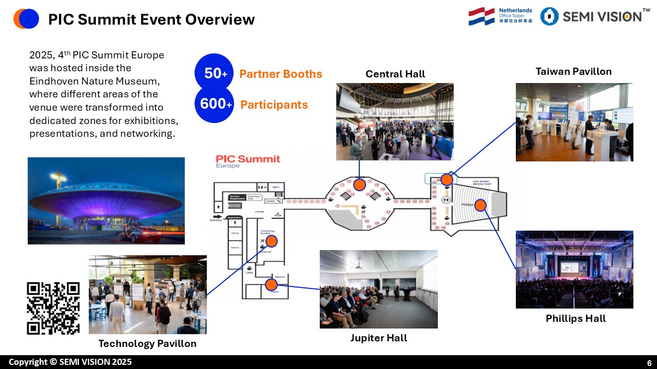
PIC Summit Europe – Event Overview
PIC Summit Europe is a leading international event dedicated to integrated photonics and photonic integrated circuits (PICs), bringing together the global ecosystem across technology, manufacturing, applications, and system integration. The summit serves as a high-level platform where industry leaders, researchers, startups, system companies, and policymakers exchange insights on how photonics is shaping the future of computing, communications, sensing, and beyond.
The 4th PIC Summit Europe, held in 2025, took place at the Eindhoven Nature Museum, a unique venue that reflects the event’s emphasis on innovation, collaboration, and cross-disciplinary thinking. The venue was transformed into multiple dedicated zones for exhibitions, technical presentations, keynote sessions, and professional networking, enabling close interaction across the entire value chain.
The event welcomed over 600 participants from across Europe and around the world, with more than 50 partner booths representing photonic chip designers, foundries, materials suppliers, packaging houses, system integrators, and research institutes. This strong participation highlights the rapid momentum of integrated photonics as it moves from research into large-scale industrial deployment.
PIC Summit Europe is designed to bridge technology and application. Rather than focusing solely on devices or fabrication, the summit emphasizes system-level impact, addressing how photonics enables next-generation data centers, AI infrastructure, co-packaged optics, sensing, LiDAR, quantum technologies, and emerging photonic computing architectures.
The event layout supports this mission. The Central Hall functions as the core exhibition and networking space, encouraging spontaneous technical discussions and cross-company collaboration. Specialized areas such as the Technology Pavilion highlight cutting-edge developments from startups and research organizations, while dedicated presentation halls—including Jupiter Hall and Philips Hall—host keynotes, panel discussions, and in-depth technical sessions.
A notable feature of PIC Summit Europe is its strong emphasis on ecosystem building. The summit actively promotes collaboration between regions, with themed pavilions—such as the Taiwan Pavilion—showcasing national and regional strengths in photonics, semiconductors, and advanced manufacturing. This international perspective reinforces the idea that integrated photonics is a global effort, requiring coordination across borders, supply chains, and disciplines.
Beyond technology, PIC Summit Europe also addresses commercialization, scalability, and manufacturability, discussing how photonics can transition from pilot lines to high-volume production. Topics such as standardization, packaging, reliability, materials, and supply-chain readiness are integral to the program, reflecting the industry’s shift from “can we build it” to “how do we scale it.”
PIC Summit Europe is more than a conference—it is a strategic meeting point for the integrated photonics ecosystem. By combining technology depth, application focus, and international collaboration, the summit plays a critical role in accelerating the adoption of photonic integrated circuits and shaping the future of high-performance, energy-efficient systems.

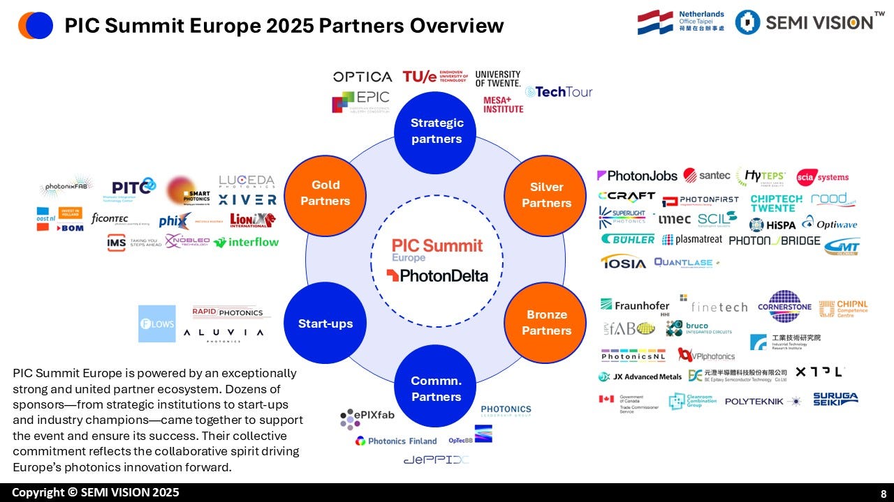
Scaling Together: Why the Next Wave of Innovation Demands Ecosystem-Level Collaboration
The semiconductor and photonics industries are entering a phase where individual excellence is no longer sufficient. As AI, high-performance computing (HPC), and data-centric workloads accelerate, the challenges facing the industry are no longer confined to a single layer of technology. Performance, power, bandwidth, cost, and manufacturability are now tightly interlinked across design, materials, photonics, packaging, and system architecture.
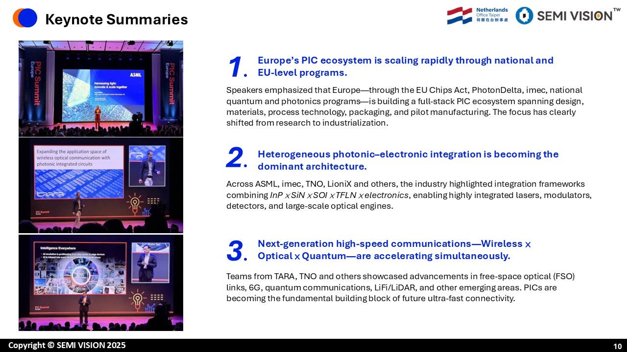
This is the context behind the 2025 PIC Summit Europe theme: Scaling Together.
In previous technology cycles, leadership could be achieved by advancing one domain faster than others—smaller transistors, faster lithography, or higher clock speeds. That model no longer works. Today’s breakthroughs depend on whether entire ecosystems can move in sync, aligning roadmaps and co-developing solutions that are manufacturable at scale.
From Moore’s Law to System-Level Scaling
For decades, Moore’s Law provided a clear and predictable scaling path. As transistors shrank, performance improved, costs fell, and energy efficiency followed. But as physical and economic limits became apparent, the industry pivoted toward heterogeneous integration, chiplets, advanced packaging, and photonic interconnects.
This shift fundamentally changes how innovation happens.
Scaling is no longer driven by transistor density alone. Instead, it depends on how well different technologies interact:
Advanced logic and memory
Photonic and electrical interconnects
Packaging architectures
Thermal and power management
Materials and manufacturing processes
Each of these domains has its own constraints and development cycles. If they evolve independently, the result is friction, delays, and suboptimal system performance. Scaling today is therefore not a node problem—it is a coordination problem.
Photonics as a System Enabler, Not a Standalone Solution
Silicon photonics has moved from research to deployment, driven by the urgent need to overcome electrical I/O bottlenecks. As data rates approach and exceed hundreds of gigabits per second per lane, copper interconnects struggle with power loss, reach limitations, and signal integrity.
However, photonics alone is not a silver bullet.
The success of photonic integration depends on close coordination with:
Packaging technologiesthat can handle optical, electrical, and thermal interfaces simultaneously
Materialswith suitable optical, mechanical, and reliability properties
Manufacturing ecosystemscapable of volume production and testing
This is why optical interposers, co-packaged optics (CPO), and hybrid integration approaches are gaining attention. They represent not just a photonics roadmap, but a system-level rethinking of how compute, memory, and connectivity are assembled.
Packaging Moves to the Center of the Value Chain
Advanced packaging has become one of the most strategic battlegrounds in the semiconductor industry. Technologies such as CoWoS, 2.5D/3D integration, fan-out, and panel-level packaging are no longer incremental improvements—they are essential to system scaling.
Packaging now determines:
Power delivery efficiency
Signal integrity at extreme bandwidths
Thermal performance
Yield and cost at the system level
As a result, the boundary between “chip design” and “system design” is blurring. Packaging engineers, materials scientists, photonics experts, and system architects must work together from the earliest design stages. Late-stage integration is simply too costly and too risky.

2025年4月11日
Materials: The Quiet Constraint on Scaling
While much attention is paid to chips and architectures, materials are increasingly the hidden limiter—or enabler—of progress.
Advanced packaging and photonics place unprecedented demands on materials:
Ultra-low dielectric loss
Precise thermal expansion control
High mechanical stability
Long-term reliability under extreme power densities
These requirements cannot be met by legacy materials alone. They require co-development between material suppliers, equipment vendors, and device manufacturers, often tailored to very specific applications.
This is where ecosystem collaboration becomes non-negotiable. Materials innovation without process alignment fails. Process innovation without materials readiness stalls. Scaling only happens when both move together.
AI has magnified all existing constraints.
Training and inference workloads are pushing systems to extremes in power consumption, bandwidth demand, and deployment scale. Data centers are now designed around entire racks and clusters, not individual chips. Power delivery, cooling, and interconnects are becoming system-level challenges.
As Sam Altman has noted, AI progress depends on global access to compute and global collaboration. No single company, country, or discipline can solve these challenges alone. The AI era demands not just faster hardware, but coordinated infrastructure development, from silicon and photonics to energy and manufacturing.
Why “Scaling Together” Is More Than a Slogan
The message behind “Scaling Together” is pragmatic, not philosophical.
Peter Wennink of ASML captured it succinctly:Innovation only works when ecosystems innovate together.Similarly, imec’s leadership has emphasized that the future of chips will be defined by global collaboration, not isolated competition.
This collaboration does not mean uniformity. Different regions and companies will continue to specialize. What must change is the way roadmaps are aligned:
Foundries with packaging and materials
Photonics with system architecture
Research institutes with industrial manufacturing
Breakthrough ideas only matter if they can be translated into reliable, scalable, and economically viable technologies.
Europe’s Role in a Global Ecosystem
Europe plays a unique role in this landscape. With strengths in photonics, equipment, materials science, and collaborative research models, Europe is well positioned to act as aconnector within the global semiconductor ecosystem.
Events like PIC Summit Europe are not just conferences—they are platforms for alignment. They bring together stakeholders who rarely sit at the same table, enabling early dialogue that can shorten development cycles and reduce integration risk.

The Future Is Built Together
The next phase of semiconductor and photonics innovation will not be defined by who moves fastest in isolation, but by who collaborates most effectively.
Scaling together means:
Designing with integration in mind from day one
Aligning roadmaps across disciplines and organizations
Treating materials, packaging, and photonics as strategic enablers, not afterthoughts
In the AI era, innovation is no longer a relay race. It is a synchronized effort—where progress only happens if everyone moves forward, together.

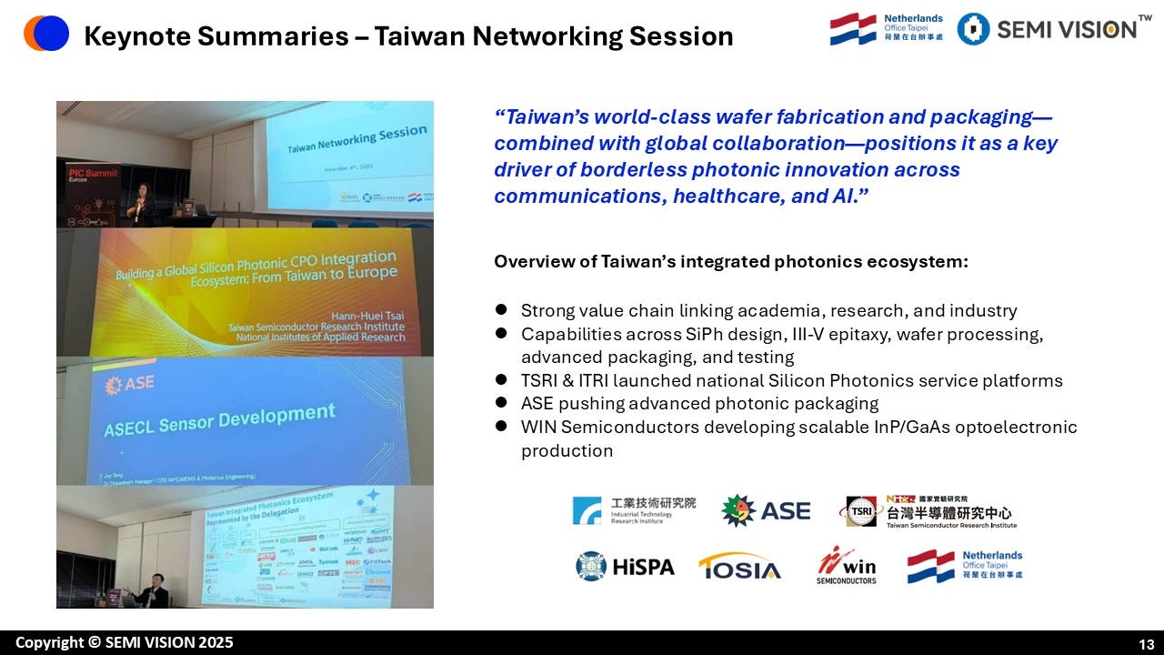
Next, we introduced Taiwan’s integrated photonics ecosystem, highlighting how its world-class wafer fabrication and advanced packaging capabilities—combined with strong global collaboration—position Taiwan as a key driver of cross-border photonic innovation across communications, healthcare, and AI. We outlined Taiwan’s tightly connected value chain linking academia, research institutes, and industry, along with its strengths in silicon photonics design, III–V epitaxy, wafer processing, advanced packaging, and testing. We also shared recent progress, including the launch of national silicon photonics service platforms by TSRI and ITRI, ASE’s ongoing investment in advanced photonic packaging, and WIN Semiconductors’ development of scalable InP/GaAs optoelectronic manufacturing.

Industrial Development Administration Ministry of Economic Affairs (IDA): The Administration has proposed“four major pillars”as the core policy framework for the future Industrial Development Administration, aimed at driving industrial transformation and strengthening economic resilience. These pillars include:
- Implementing the President’s Five Trusted Industries policy and the “Healthy Taiwan” initiative:
By advancing AI software and hardware, strengthening the semiconductor industry value chain, and expanding applications of drones and robotics, Taiwan aims to position itself as a key partner within the global democratic technology alliance.
- Driving dual-axis industrial transformation through AI:
The Administration will vigorously promote AI adoption across all industries, helping enterprises improve efficiency and reduce costs, while cultivating and attracting AI talent needed by industry to support net-zero goals and digital transformation.
- Supporting the sustainable development of traditional industries:
Through tax incentives such as investment tax credits, the Administration will encourage dual-axis transformation in traditional industries. It will also promote cross-sector collaboration between traditional and high-tech industries to develop new technologies, products, materials, and services—enabling traditional industries to shine again on the modern industrial stage, while enhancing competitiveness and supporting global expansion.
- Promoting balanced regional development:
Guided by the President’s vision of a “Balanced Taiwan,” the Administration will foster more even industrial development across all regions, consolidating industrial strengths, leveraging cluster synergies, and enhancing local growth potential and resilience.
IDA Director-General Chiu expressed the hope that the Industrial Development Administration will become a trusted partner and the strongest backbone of Taiwan’s industries. He looks forward to working with all colleagues to open a new chapter by integrating industry, academia, research institutions, and international resources, and by striving to build an innovative, sustainable, resilient, and inclusive industrial environment.
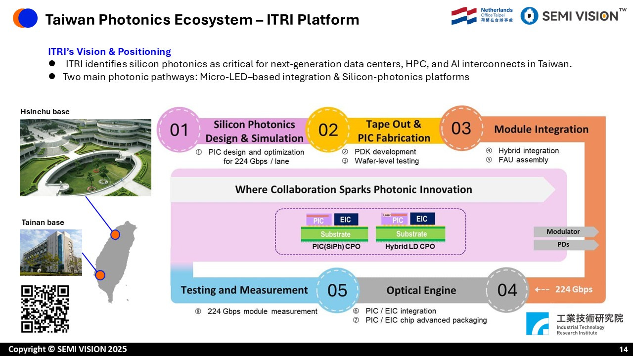
Industrial Technology Research Institute(ITRI)offers extensive Photonics services through its Electronic and Optoelectronic System Research Laboratories (EOSL), focusing on silicon photonics platforms for high-speed data, laser applications, prototyping/manufacturing, and testing, helping industries move from R&D to product development in areas like optical components, machinery, and medical devices. Key services include silicon photonics platform development (224 Gb/s), laser industry alliances, customized prototyping, reliability testing, and PV testing, all supported by their TAF-certified testing labs.
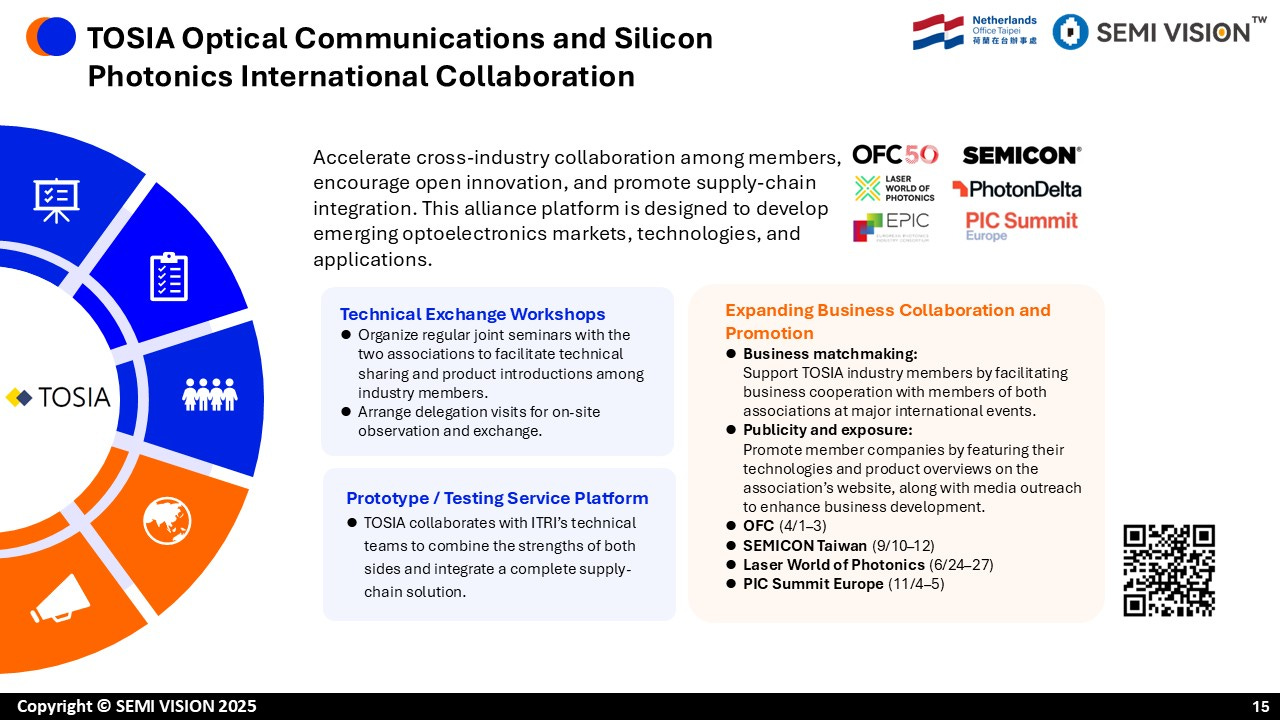
Taiwan Optoelectronic Semiconductor Industry Association(TOSIA)was founded in March 2007 aims to agglomerate domestic consensus on the development of the optoelectronic semiconductor industry, to promote strategic collaboration among its members, and to advance and bring prosperity to the industry. Meanwhile, it joins efforts with various major associations and industrial organizations, and the Industrial Technology Research Institute to develop an industrial development platform in order to provide effective technical and professional services, and to boost the overall competitive advantages of the optoelectronic semiconductor industry in Taiwan.

Heterogeneous Integration Silicon Photonics Research Center(HiSPA), establishing itself as an industry-academia matching hub for advanced and innovative technologies. It will serve as an industrial service platform for technical consultation, research achievements promotion, and technology transfer while offering high-quality membership services. With the goal of fostering industry-academia collaboration and enhancing the technological standards of domestic industries, the alliance seeks to strengthen the connection between R&D and industry. Through various measures aimed at integrating and applying research outcomes to industrial needs, the establishment of the International Heterogeneous Integration Silicon Photonics Alliance is expected to bridge the gap between academic research and industrial applications.TT

2025年6月20日
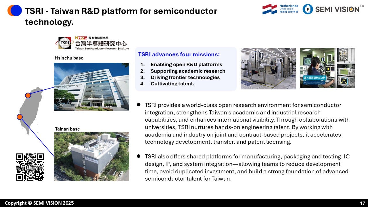
Taiwan Semiconductor Research Institute (TSRI)is positioned as a service provider of Taiwanese industry, academic, and research sectors specializing in semiconductor research. TSRI provides the only open laboratory research environment in Taiwan that is fully equipped with technologies for device manufacturing, circuit design, and system integration and employs a team of experts in life sciences, optics, electronics, machinery, circuit design, or system engineering who collaborate through various means to achieve multidisciplinary research outcomes and develop multidisciplinary techniques. By following the four main missions of NIAR (i.e., to establish research and development (R&D) platforms, support academic research, promote frontier science and technology, and attract high-tech professionals), TSRI continues to engage in the following actions with the goal of becoming a world-class research center:
TSRI is committed to the establishment of open platforms for information and services related to semiconductor manufacturing, packaging and testing, IC design, silicon intellectual property, and system integration, among others, aligning with international standards. These resources are shared among domestic academia, industry, and research teams, enhancing Taiwan's research capacity in integrated component technology. TSRI aims to become an accelerator for semiconductor research in Taiwan's academia, industry, and research sectors, fostering advanced doctoral and master's level research talents through collaborative efforts.
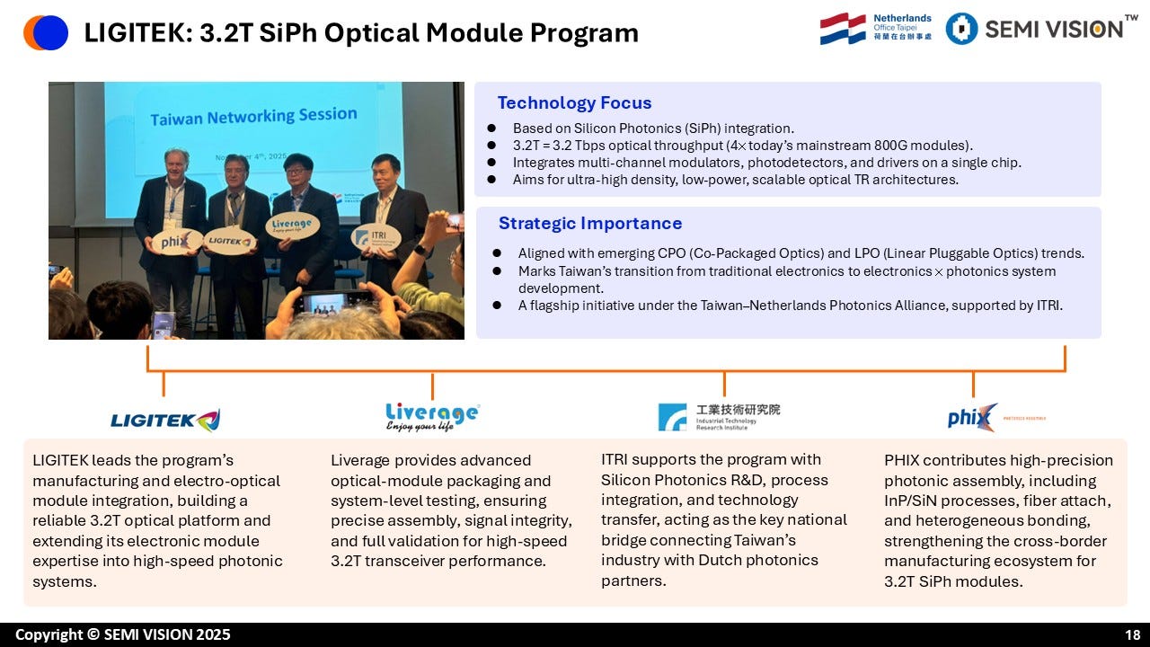
PHIX, Ligitek, Liverage, and ITRI have partnered to develop next-generation high-speed and energy-efficient optical transceivers to address global challenges in data connectivity. This advancement in high-speed optical engines strengthens the Netherlands-Taiwan collaboration and prepares new semiconductor packaging innovations for scalable volume manufacturing.
PHIX Partners with ITRI, Ligitek, and Liverage from Taiwan to Advance High-Speed Optical Engines
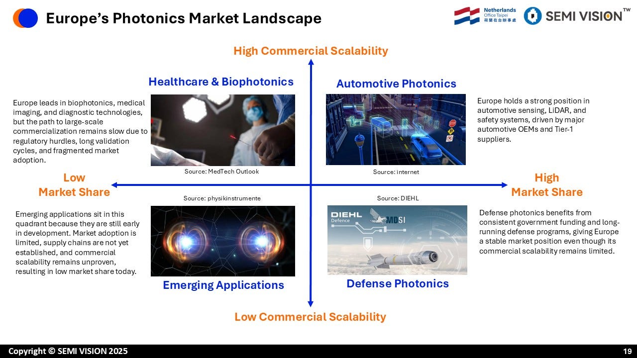
Europe’s High-Scalability Photonics Segments: From Technology Leadership to Market Expansion
Within Europe’s photonics ecosystem, high commercial scalability is concentrated in application areas where technological maturity, strong industrial integration, and clear demand drivers converge. Among these, Healthcare & Biophotonics and Automotive Photonics stand out as the most scalable and economically impactful segments.
Healthcare & Biophotonics: Strong Technology, Expanding Adoption
Europe holds a global leadership position in biophotonics, medical imaging, diagnostics, and laser-based medical technologies. Decades of investment in optics, lasers, and precision instrumentation have resulted in highly sophisticated solutions for imaging, sensing, and minimally invasive procedures.
From a scalability perspective, healthcare photonics benefits from:
Aging populations and rising healthcare demand
Continuous innovation in diagnostics and imaging accuracy
Strong alignment with Europe’s medical device and life sciences industries
While regulatory approval processes and clinical validation cycles can slow time-to-market, once adopted, these technologies typically achieve long product lifecycles, stable margins, and global export potential. As healthcare systems increasingly emphasize early diagnosis, personalized medicine, and digital health integration, biophotonics remains one of Europe’s most commercially scalable photonics domains.
Automotive Photonics: Driven by Electrification and Autonomy
Automotive photonics represents the most direct path to large-scale commercialization. Europe’s strength in automotive manufacturing, combined with leadership in ADAS, autonomous driving, and electric vehicles, creates a robust demand foundation for photonic technologies.
Key growth drivers include:
LiDAR and optical sensing for ADAS and autonomous systems
Optical communication and sensing for in-vehicle networks
Photonics-enabled manufacturing and quality inspection
Unlike emerging photonics applications, automotive platforms benefit from high-volume production, standardized qualification processes, and long-term supplier relationships with OEMs and Tier-1 suppliers. Once designed into a vehicle platform, photonic components can scale rapidly across millions of units, offering strong cost-down potential and predictable revenue streams.
Why These Segments Scale Better Than Others
Compared with defense or early-stage emerging applications, healthcare and automotive photonics share several structural advantages:
Clear end-market demand with well-defined use cases
Established industrial ecosystems capable of scaling production
Integration into existing supply chains rather than standalone deployment
These factors reduce commercialization risk and enable photonic innovations to transition from lab-scale success to mass-market impact.
For Europe’s photonics industry, focusing on high commercial scalability does not mean abandoning long-term research or emerging fields. Instead, it means using healthcare and automotive applications as economic anchors—segments that generate revenue, justify manufacturing investment, and support ecosystem sustainability.
As global competition intensifies, Europe’s ability to scale photonics solutions in these domains will be critical not only for market leadership, but also for maintaining technological sovereignty and industrial resilience.
In the next phase of photonics growth, leadership will belong to those who can translate optical excellence into scalable, manufacturable, and globally deployable systems—and Europe’s healthcare and automotive sectors are where this translation is already happening.
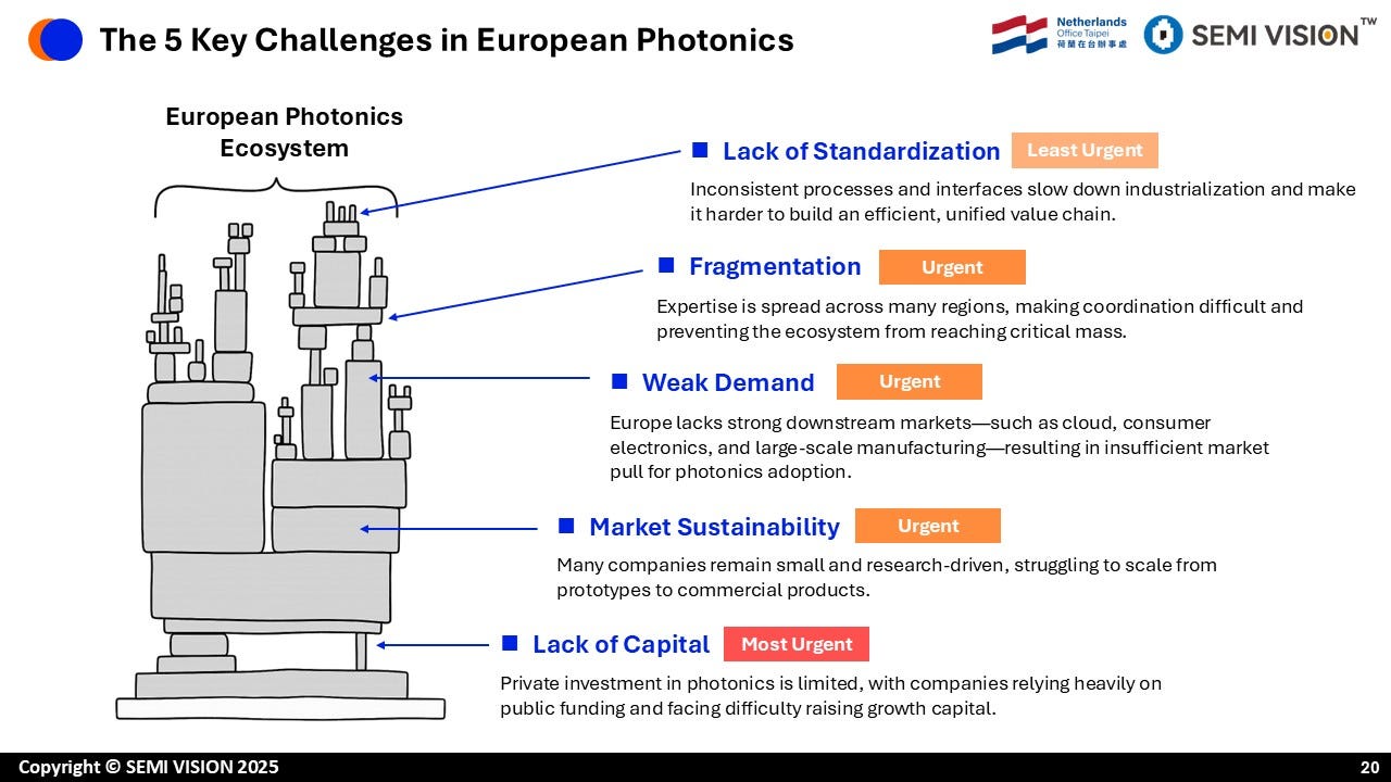
These challenges are not isolated issues, but a tightly linked chain that constrains the entire European photonics ecosystem. Fragmentation across regions and organizations makes standardization difficult, which in turn slows industrialization and increases integration costs. Weak downstream demand reduces market pull, discouraging private investment and reinforcing reliance on public funding. Without sufficient capital, companies remain small and research-driven, struggling to scale from prototypes to commercial products—further limiting market sustainability.
Because each problem reinforces the next, addressing them individually will not be sufficient. Meaningful progress requires systemic change, including better coordination across regions, aligned standards, stronger links to large downstream markets, and mechanisms to attract long-term private capital. Only by breaking this interconnected cycle can Europe translate its strong photonics research base into scalable, globally competitive industries.

Europe’s Photonics Strategy: From Research Leadership to Scalable Industrial Systems
Europe has long held a strong position in photonics and optical technologies. Across academic research, fundamental science, metrology, and key equipment and materials, Europe remains globally influential. However, as AI, high-performance computing, data centers, and advanced packaging accelerate, photonics is shifting from a supporting role to a core enabler of system performance. In this context, Europe increasingly recognizes that research excellence alone is no longer sufficient. The central strategic challenge is how to transform technological leadership into scalable, manufacturable, and sovereign industrial capabilities.
SemiVision’s analysis of Europe’s photonics landscape shows that current EU strategy can be distilled into three core pillars: building an integrated ecosystem, strengthening technological sovereignty, and aligning resources around high-impact domains. These pillars are deeply interconnected and must advance together.
- Building a Cross-Border Integrated Photonics Ecosystem
Europe’s greatest strength lies in the diversity and depth of its photonics research base. From PhotonDelta in the Netherlands and Fraunhofer in Germany to imec in Belgium and leading institutes across France and the Nordic countries, Europe covers nearly every critical node of the photonics value chain. However, this “distributed excellence” has also resulted in fragmentation.
Historically, photonics development in Europe has been driven by individual countries, institutes, or short-term projects, often lacking a unified industrial roadmap. As a result, many promising technologies failed to translate into scalable commercial platforms. In response, the EU is now actively promoting cross-border ecosystem integration—linking research, design, manufacturing, packaging, and system applications into a coherent value chain.
This integration is not merely organizational. Alignment of roadmaps, interfaces, and standards is essential. Without it, duplication of effort and inefficient capital deployment persist. Only through coordinated development can Europe build a photonics ecosystem with true global competitiveness.
- Closing the Industrialization Gap Through Pilot Lines
Compared with the United States and Asia, Europe’s most visible weakness in photonics is not innovation, but manufacturing scale-up capability. Many European photonics startups and technologies remain stuck at the prototype or low-volume stage, unable to cross the “valley of death” between lab success and market adoption.
To address this, the EU has significantly expanded investment in pilot line programs such as PIXAPP, JePPIX, and other photonics pilot initiatives. These platforms sit between research and mass production, allowing companies to validate process stability, yield, reliability, and cost structures under industrial conditions.
Crucially, pilot lines are designed as shared infrastructure, not proprietary assets. This lowers market entry barriers for startups and SMEs while enabling Europe to accumulate manufacturing know-how at the ecosystem level—an essential prerequisite for long-term industrial competitiveness.
- From Research Independence to Manufacturing Sovereignty
Europe has traditionally emphasized research autonomy as the foundation of technological sovereignty. However, amid rising geopolitical risks and supply-chain disruptions, it has become clear that research independence alone does not guarantee strategic autonomy. If key manufacturing and packaging steps remain dependent on external partners, control over critical technologies is fundamentally limited.
As a result, Europe’s photonics strategy is expanding beyond R&D to include domestic capabilities in packaging, testing, and volume manufacturing. This shift is particularly important for silicon photonics and advanced packaging, where system performance increasingly depends on heterogeneous integration.
In an era where photonics and semiconductors are deeply intertwined, packaging has become a decisive factor for power efficiency, bandwidth, and reliability. Without local capabilities in these areas, Europe risks structural dependence on external foundries and OSATs.
- Aligning Resources Through Strategic Focus
Perhaps the most difficult challenge is resource alignment. Europe has historically spread funding across too many initiatives, diluting impact and limiting scale advantages. Facing the rapid rise of AI and system-level innovation, the EU is now re-evaluating its investment strategy—shifting from broad dispersion to targeted concentration.
Silicon photonics has emerged as a priority domain. It aligns closely with Europe’s strengths in equipment, materials, and research, while directly serving high-growth markets such as AI infrastructure, data centers, communications, and advanced packaging. By focusing resources on areas with long-term strategic leverage, Europe aims to build positions that are structurally difficult to replace.
From Technology Leadership to Industrial Leadership
At its core, Europe’s photonics strategy is not about short-term acceleration, but structural transformation for long-term competitiveness. Ecosystem integration, manufacturing enablement, technological sovereignty, and focused investment all serve a single objective: enabling Europe to move beyond being a source of innovation to becoming a scalable, industrial leader in photonics.
In the AI-driven era of system-level competition, leadership is no longer defined by isolated breakthroughs, but by the ability to coordinate across the entire value chain. Whether Europe succeeds in this transition will play a decisive role in shaping the global photonics and semiconductor landscape over the next decade.
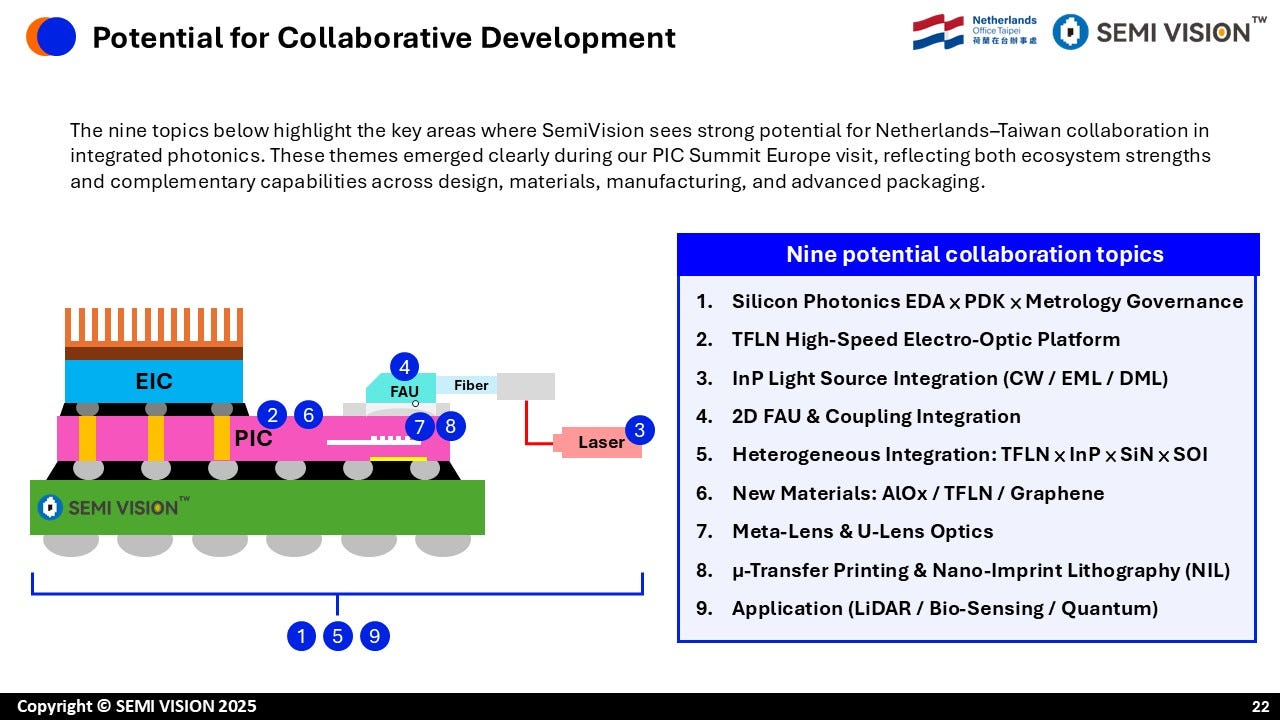
Potential Areas for Collaborative Development in Integrated Photonics
The following themes highlight key areas where strong potential exists for Netherlands–Taiwan collaboration in integrated photonics, as identified through in-depth ecosystem analysis and discussions during our recent engagements, including the PIC Summit Europe visit. These topics reflect complementary strengths across design, materials, manufacturing, and advanced packaging, and represent concrete opportunities for joint development.
Silicon Photonics EDA, PDK, and metrology governanceform the foundation of scalable photonic manufacturing. Alignment in design tools, process design kits, and measurement standards is essential for enabling cross-foundry compatibility and accelerating productization.
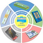
Thin-Film Lithium Niobate (TFLN) high-speed electro-optic platformsare emerging as a critical enabler for next-generation modulators, offering superior bandwidth, efficiency, and low-loss characteristics for high-speed optical interconnects.
InP light source integration, including CW, EML, and DML lasers, remains a key bottleneck and opportunity. Close collaboration is required to bridge III–V light sources with silicon-based platforms in a manufacturable and scalable way.
2D FAU and advanced coupling integrationaddress packaging-level challenges, enabling more efficient fiber-to-chip and chip-to-chip optical interfaces with tighter tolerances and higher yields.
Heterogeneous integration across TFLN, InP, SiN, and SOIrepresents the system-level future of photonics, combining the strengths of multiple material platforms to optimize performance, power efficiency, and functionality.
New materials, such as AlOx, advanced TFLN variants, and graphene, open new design spaces for low-loss waveguides, modulators, detectors, and novel optoelectronic functions.
2025年5月15日
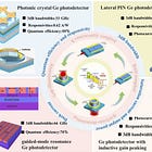
Meta-lens and ultra-thin lens (U-lens) opticsprovide compact, high-performance optical solutions that are increasingly relevant for sensing, imaging, and AR/VR applications.

2025年12月23日
µ-transfer printing and nanoimprint lithography (NIL)are key process technologies for cost-effective, high-throughput manufacturing of photonic and nano-optical structures, enabling volume production beyond pilot-scale demonstrations.

2025年11月29日
Applications spanning LiDAR, biosensing, and quantum technologiesserve as important pull drivers, translating platform and process innovations into real-world systems and markets.
These areas are not isolated research topics, but interconnected building blocks of a next-generation integrated photonics ecosystem. If your company or organization is interested in joint development, strategic collaboration, or ecosystem-level partnerships, we warmly invite you to contact us to explore concrete collaboration opportunities.
Contact email: jett@semivisiontw.com

Taiwan’s Semiconductor Transformation
Taiwan’s semiconductor industry has undergone a profound transformation, evolving from a manufacturing-driven model into a global hub for innovation and co-creation.
In the past, Taiwan established its global leadership through manufacturing excellence. With world-class fabrication capabilities, high yields, reliable supply chains, and advanced process control, Taiwan became the foundation of the global semiconductor industry. During this stage, the focus was on “Made in Taiwan”, supplying conventional chips at unmatched scale and quality.
In the present, Taiwan’s role has expanded beyond pure manufacturing into innovation and engineering strength. As AI chips and advanced computing platforms drive complexity higher, Taiwan increasingly contributes engineering know-how, design collaboration, and process optimization. This phase—“Made by Taiwan”—reflects Taiwan’s growing involvement in co-development with global partners, particularly in advanced packaging, system integration, and performance-driven manufacturing.
Looking toward the future, Taiwan is positioning itself as a strategic partner in global co-creation. Under the vision of “Made with Taiwan”, the next stage emphasizes deep partnerships with Europe, the United States, and Asia to co-develop frontier technologies such as silicon photonics, quantum chips, 3D packaging, and heterogeneous integration. Taiwan’s role shifts from being a manufacturing backbone to becoming a co-architect of future semiconductor platforms.
This evolution is not a replacement of past strengths, but a layered progression—from manufacturing excellence, to engineering-driven innovation, and ultimately to ecosystem-level co-creation—defining Taiwan’s long-term strategic position in the global semiconductor landscape.

2025年4月6日
How Taiwan and the Netherlands Are Building a New Model of Semiconductor Collaboration
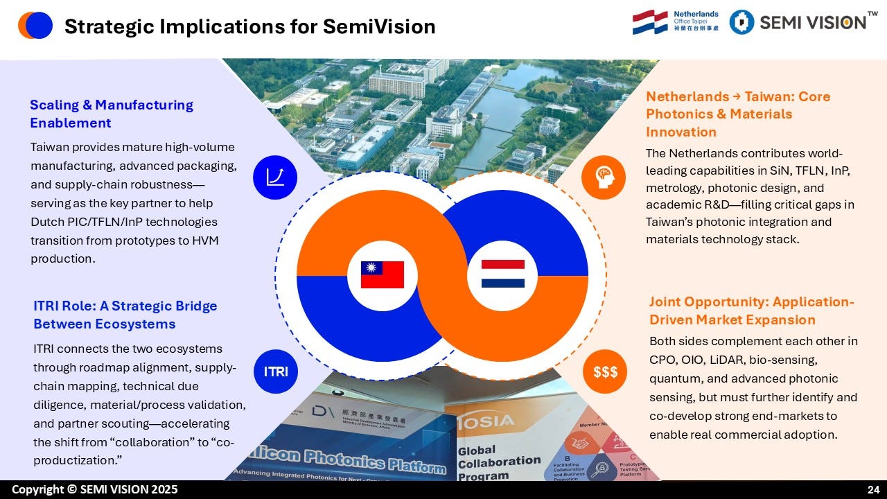
The collaboration between Taiwan and the Netherlands represents a shift from traditional supply-chain relationships toward a co-creation–driven partnership in advanced semiconductors and integrated photonics. Rather than duplicating capabilities, both sides contribute highly complementary strengths—creating a model that is increasingly relevant as the industry moves into an era defined by system complexity, heterogeneous integration, and application-driven innovation.
Taiwan’s semiconductor evolution provides the foundation for this collaboration. Historically, Taiwan established global leadership through manufacturing excellence, delivering world-class yields, reliability, and scale. Over time, this role expanded into engineering-driven innovation, particularly in advanced packaging, process integration, and system optimization for AI and high-performance computing.
Today, Taiwan is entering a new phase:“Made with Taiwan.”In this stage, Taiwan is no longer only a manufacturing backbone, but a strategic co-creator—working with global partners to jointly architect future technologies such as silicon photonics, 3D integration, chiplet systems, and emerging quantum platfor
The Netherlands: Core Innovation in Photonics and Materials
The Netherlands brings deep strengths in integrated photonics, advanced materials, metrology, and design methodologies. Its ecosystem spans silicon photonics, thin-film lithium niobate (TFLN), InP light sources, precision optics, and nano-fabrication—supported by a strong link between academia, research institutes, and industry.
These capabilities address some of the most critical gaps in next-generation systems:
How to integrate light sources with silicon platforms
How to scale novel photonic materials beyond the lab
How to design, measure, and standardize increasingly complex photonic systems
In short, the Netherlands contributes core innovation and upstream technology depth that is essential but difficult to industrialize alone.
2025年6月16日
Taiwan: Scaling, Packaging, and Manufacturing Enablement
This is where Taiwan becomes indispensable. Taiwan provides the ability to translate advanced concepts into high-volume manufacturing, supported by mature supply chains, advanced packaging technologies, and proven execution at scale.
For emerging photonic and heterogeneous integration technologies, the biggest barrier is often not performance—but manufacturability, yield, reliability, and cost. Taiwan’s ecosystem is uniquely positioned to solve these challenges, helping Dutch-developed technologies transition from prototypes to commercial products.
Advanced packaging, co-design with manufacturing, materials qualification, and supply-chain robustness form the backbone of this enablement role.
A critical element in this partnership is ecosystem alignment. Collaboration at this level requires more than bilateral company partnerships—it demands roadmap coordination, supply-chain mapping, technical validation, and partner sourcing across borders.
This bridging function ensures that innovation does not stall at the interface between research and production. It accelerates the shift from “collaboration” to true co-production, where risks, development effort, and long-term value are shared
The ultimate goal of Taiwan–Netherlands collaboration is not technology for its own sake, but application-driven market adoption. Both sides bring complementary strengths to emerging markets such as:
Co-Packaged Optics (CPO) and optical I/O
AI and HPC interconnects
LiDAR and advanced sensing
Bio-sensing and medical photonics
Quantum and next-generation computing platforms
By jointly identifying target applications and co-developing end-to-end solutions—from materials and devices to packaging and manufacturing—the partnership can overcome the “valley of death” between innovation and commercialization.
A Blueprint for the Next Semiconductor Era
As semiconductor systems become more complex and interdisciplinary, no single country or ecosystem can succeed alone. The Taiwan–Netherlands partnership illustrates a new blueprint:
Taiwan enables scale, integration, packaging, and manufacturing execution
Together, they co-create technologies that neither could commercialize as effectively on their own
This is not a zero-sum relationship. It is a strategic convergence, aligning innovation depth with industrial scale—defining how advanced semiconductor ecosystems will collaborate in the decade ahead.
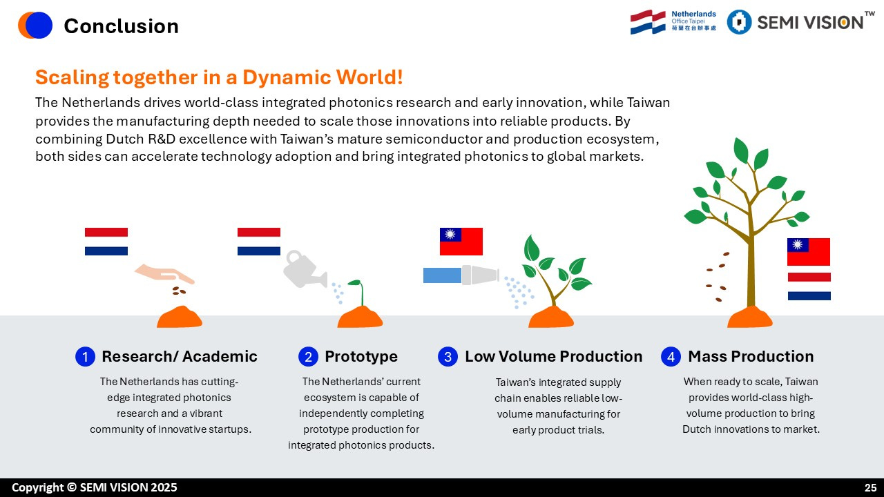
By combining the Netherlands’ strengths in cutting-edge integrated photonics research and early-stage innovation with Taiwan’s depth in manufacturing, advanced packaging, and production ecosystems, both sides create a powerful pathway from research to mass production. This complementary partnership enables faster technology scaling, reduces commercialization risk, and brings integrated photonics innovations efficiently to global markets.


2025年12月31日


PreviousNext
TopLatestDiscussions








See all