Thank You for Being Part of SemiVision’s 2025 Journey
Thank You for Being Part of SemiVision’s 2025 Journey
- Source: SemiVision
- Author: SEMIVISION
- Published: 2025-12-31T23:30:42+08:00
- URL: https://tspasemiconductor.substack.com/p/thank-you-for-being-part-of-semivisions Thank You for Being Part of SemiVision’s 2025 Journey


Thank You for Being Part of SemiVision’s 2025 Journey
Original Article By SemiVision Research

Dec 31, 2025
∙ Paid
SemiVision has just completed its first year, and the pace of growth has been remarkable.
What has stood out most is the strong enthusiasm across our community for learning and understanding new developments in semiconductors. This shared curiosity and drive for deeper knowledge are exactly what motivate us to keep pushing forward—and they define the direction of our continued efforts.
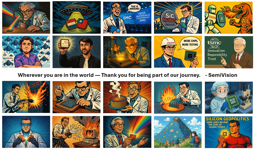
In 2025, we set ambitious goals—and delivered.
and surpassed1.5 million total views.
Our work earned recognition as aTop 10 Technology publication,
while our team actively engaged in30+ global technical forums,
traveling across10+ cities worldwideto stay at the forefront of innovation.
These milestones are more than numbers.
They reflect our commitment to rigorous analysis, global perspective,
and a clear belief that deep insights drive better decisions.

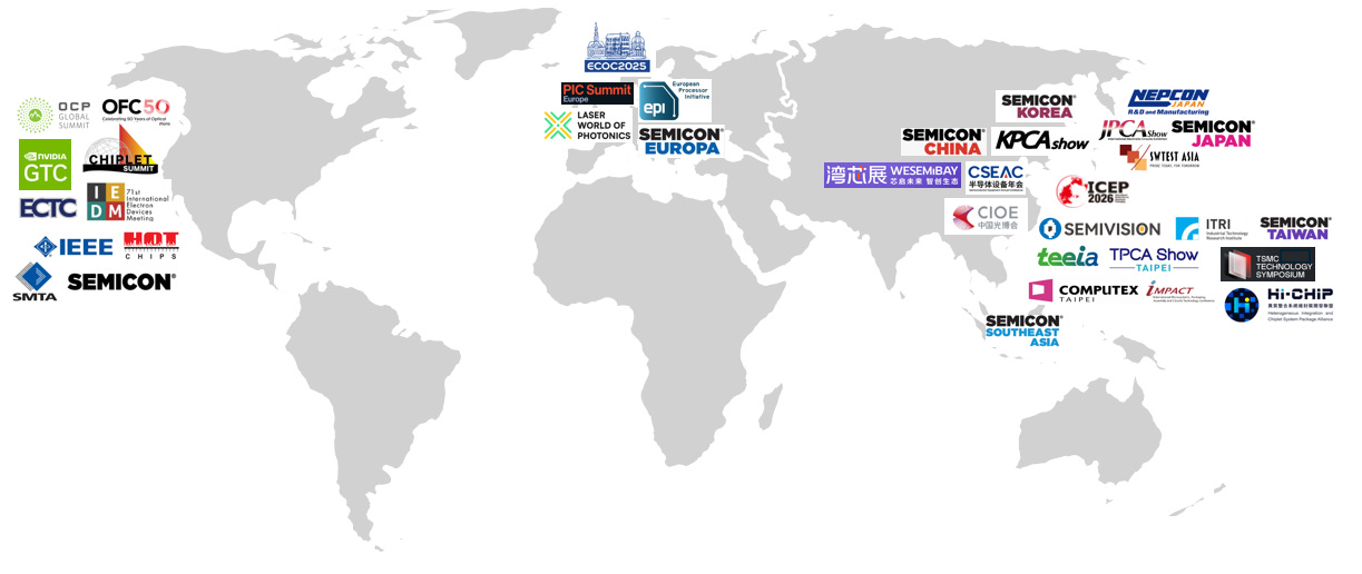
SemiVision remains deeply committed to participating in leading global technology forums and industry conferences. By staying on the front lines of semiconductor and photonics innovation, we aim to continuously bring our community the latest technologies, emerging trends, and actionable insights. Our goal is simple: to turn first-hand industry engagement into clear, forward-looking knowledge that helps our readers and partners stay ahead in a rapidly evolving landscape.
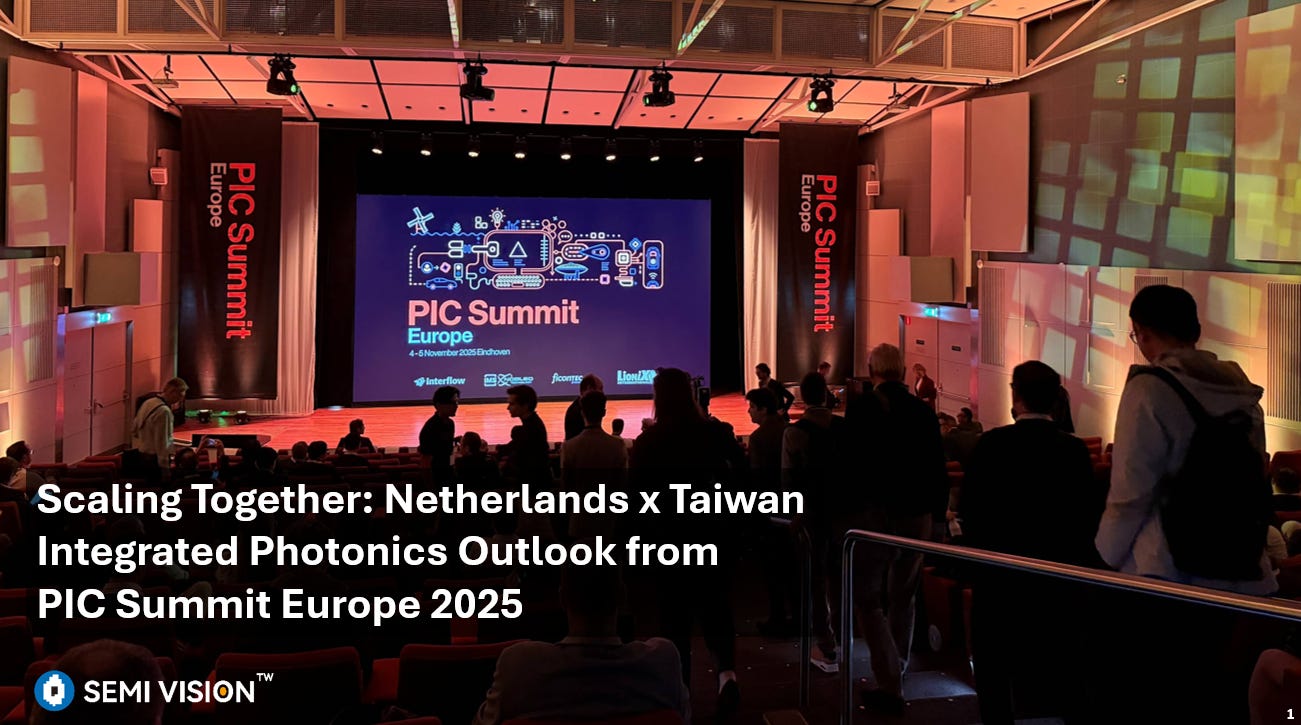
In November this year, SemiVision collaborated with the Netherlands Office in Taipei (NLOT) as part of the Taiwan Delegation to the Netherlands, joining the visit to Eindhoven for PIC Summit Europe. As a participant in the delegation, SemiVision will actively support event promotion, on-site activity coverage, and post-event documentation, delivering structured event reports, ecosystem mapping, and in-depth industry analysis white papers focused on integrated photonics and next-generation semiconductor technologies.

We also welcome event organizers, ecosystem managers, and industry partners who are planning similar activities or international delegations to reach out to SemiVision. Our team provides customized promotion, technical content, and strategic industry insights to help maximize the impact and long-term value of cross-border technology events.

2025年10月24日

2025年11月12日
Top 5 Most-Viewed Articles of 2025:

2025年10月5日

2025年11月29日

2025年10月13日
2025年6月2日

2025年5月27日
Top 5 Defining Technology Topics of 2025 — and Why They Matter
- Advanced Packaging
As Moore’s Law slows at the transistor level, performance gains increasingly come from packaging. Technologies such as CoWoS, chiplets, 3D stacking, and heterogeneous integration became decisive factors in scaling AI and HPC systems—directly impacting yield, cost, power delivery, and time-to-market.
- Silicon Photonics
Electrical interconnects reached their physical and energy limits in data centers. Silicon photonics emerged as a critical enabler for scaling AI infrastructure, offering higher bandwidth, lower power consumption, and longer reach—reshaping how data moves within and between servers.
- Thermal Challenges
With AI processors exceeding kilowatt-level power envelopes, thermal management evolved from an engineering constraint into a system-level bottleneck. Advanced cooling, thermal materials, and co-design across chip, package, and system became essential to sustaining performance and reliability.
- TSMC × NVIDIA Ecosystem
The deepening collaboration between TSMC and NVIDIA highlighted a new industry reality: leading-edge compute is no longer about a single company, but about tightly integrated ecosystems spanning process nodes, advanced packaging, supply chains, and capacity planning.
- AI Chips
AI workloads redefined chip architecture. From GPUs and custom accelerators to domain-specific ASICs, AI chips drove unprecedented demand for compute density, memory bandwidth, and energy efficiency—reshaping semiconductor roadmaps across foundries, OSATs, and materials suppliers.
At SemiVision, we focus on the full semiconductor and photonics value chain—where materials, processes, devices, and systems converge.
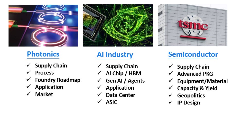
Our research spans advanced packaging, silicon photonics, materials innovation, IC substrates, thermal solutions, manufacturing processes, supply-chain dynamics, and AI-driven system architectures.
In the AI era, semiconductor innovation is no longer about isolated breakthroughs, but about system-level collapse and reconstruction. For the past three decades, the industry’s progress followed a relatively simple logic: process scaling delivered performance gains, and advances in CMOS nodes were almost synonymous with overall industry growth. That path is now breaking down. As transistors evolved from planar MOSFETs to FinFETs and then to GAA, and as nodes pushed toward 2 nm and even the angstrom scale, the industry has, for the first time, clearly recognized that the performance ceiling no longer lies within CMOS itself, but in system integration capability.
Against this backdrop, hybrid bonding, advanced packaging, silicon photonics, HBM, glass substrates, CPO, power delivery, and thermal management are no longer optional value-add technologies. They are tightly coupled, mutually dependent system components—none can be missing. The semiconductor industry must fundamentally rethink the structure and logic of the entire technology puzzle.
Hybrid bonding is viewed as a watershed in advanced packaging not because it is merely “more advanced,” but because it fundamentally changes the physical scale of interconnects. While traditional micro-bumps are constrained by pitch, parasitic capacitance, and power consumption, hybrid bonding pushes interconnects to sub-10 µm—and even a few-micron—scales, making logic-on-logic integration, HBM stacking, and chiplet architectures truly scalable. At the same time, this shift triggers a cascade of new challenges: whether CMP planarity is sufficient for Cu-Cu and oxide-oxide bonding, how alignment errors can be controlled at the nanometer level, and whether backside power delivery networks (BSPDN) become a necessity rather than an option. Hybrid bonding has never been a single process; it is a central node that reshapes the entire system engineering stack.

2025年7月13日
In parallel, AI servers and accelerators face another reality: the energy cost and bandwidth of electrical interconnects—within packages, between packages, and across racks—are no longer proportional. This is the fundamental reason silicon photonics has moved to center stage. Yet the hardest questions are not whether optics can be used, but which platforms—Si, SiN, InP, or thin-film lithium niobate (TFLN)—make sense at the system level, what the architectural differences between CPO and OIO truly are, and how opto-electronic co-packaging can be aligned, tested, and mass-produced. As optical I/O moves toward on-package and chip-to-chip links, testing and coupling themselves become the largest bottlenecks to commercialization.
2025年6月16日
The constraints of AI systems are not limited to interconnects and compute. Power and materials form a more hidden yet lethal battlefield. AI chips are not simply computing; they are consuming enormous power density and generating extreme heat. This is why SiC power devices are entering data centers and AI server power architectures, why ceramic materials such as AlN and Si₃N₄ are indispensable in high-power modules, and why TIMs have evolved from simple gap-fillers into integral elements of system-level thermal design. When power density exceeds 2–3 W/mm², cooling and material choices directly determine whether a system can scale at all.

2025年9月21日
Glass substrates and TGVs are often compared directly with silicon interposers, but this is the wrong question. The real issue is how warpage, planarity, and dielectric loss can be controlled as package sizes continue to grow, and whether materials themselves become system-level constraints when high-speed I/O and optical waveguides must coexist. The value of glass has never been about being cheaper; it lies in lower CTE, superior planarity, and physical properties better suited for opto-electronic integration—while simultaneously introducing new challenges in drilling, metallization, reliability, and high-volume manufacturing equipment.

2025年6月30日
If the technologies discussed above can still be viewed as options, AI servers are the reality where all options are bundled and amplified simultaneously. In AI servers, HBM, chiplets, and CPO coexist; PCBs, substrates, and packages must be co-designed at the system level; the boundary between OSATs and foundries becomes blurred; and testing complexity increases exponentially. This directly reshapes the entire supply-chain structure—from WFE investment cycles and ABF substrate capacity to platform-level competition in advanced packaging.

2025年8月25日
The real question is no longer whether one understands a specific technology. It is whether one can see the entire structure. You may be deeply familiar with hybrid bonding, silicon photonics, HBM, or glass substrates individually, but the true risk in the AI era is understanding only one piece while critical decisions are made at the intersections of the puzzle. This is precisely why the SemiVision Tech Insight Report exists. It does not merely introduce technologies; it answers which technologies are no longer choices but inevitabilities, which bottlenecks lie not within a single discipline but at the interfaces across the value chain, and which changes will first impact cost, then yield, and ultimately reshape industry competition.
SemiVision does not simply discuss hybrid bonding, silicon photonics, HBM, or glass substrates in isolation. It analyzes how these technologies amplify, constrain, and enable one another. If you are working on technology strategy, investment decisions, supply-chain positioning, or AI infrastructure planning, what you truly need is not another article, but a system map that makes the next three to five years intelligible. That is the core value of the SemiVision Tech Insight Report.

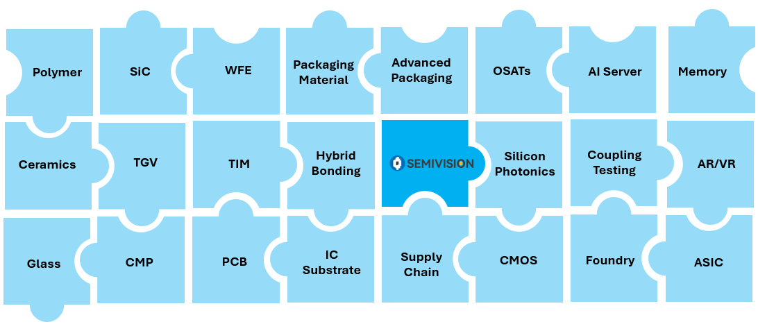
SemiVision application puzzle: each piece represents a critical domain—from materials and packaging, to photonics, devices, and system-level trends. By assembling these pieces, we uncover how technologies interconnect, where bottlenecks form, and where the next wave of opportunities is emerging.
Our goal is not just to describe the industry, but to translate complexity into actionable insight.
We welcome inquiries for customized reports tailored to your specific technology focus, market segment, or strategic questions. SemiVision delivers independent, in-depth analysis designed to support informed decision-making in a rapidly evolving landscape.
SemiVision focuses on delivering high-depth, actionable semiconductor industry technology analysis for enterprise clients, enabling Business Development (BD) and Market Intelligence (MI) teams to quickly grasp future technology directions and critical industry inflection points amid highly uncertain technological evolution.
Our research goes beyond surface-level technical descriptions. We systematically connect process nodes, packaging architectures, material roadmaps, supply-chain roles, and end-application scenarios, allowing companies to translate technology trends directly into commercial judgment, partnership strategies, and investment decisions.
In addition, SemiVision provides highly customized research services, tailoring analytical frameworks and decision perspectives to each client’s product positioning, market role, and strategic objectives, ensuring that insights are both relevant and immediately usable.
Thank You to Our Global Community
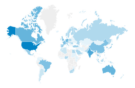
None of this would be possible without you.
This diversity is not just a statistic. It reflects a shared curiosity and a collective commitment to understanding complex topics with depth, rigor, and clarity. Different perspectives, markets, and experiences strengthen the conversations we build together.
Thank you for reading, sharing, challenging ideas, and staying engaged. Your trust motivates SemiVision to continue delivering thoughtful analysis, forward-looking insights, and honest exploration of the technologies that matter.
Wherever you are in the world—thank you for being part of our journey.


PreviousNext
TopLatestDiscussions








See all