From Chips to Optics: TSMC’s Metalens Strategy Signals a New Integration Wave
From Chips to Optics: TSMC’s Metalens Strategy Signals a New Integration Wave
- Source: SemiVision
- Author: SEMIVISION
- Published: 2025-12-23T22:01:40+08:00
- URL: https://tspasemiconductor.substack.com/p/from-chips-to-optics-tsmcs-metalens From Chips to Optics: TSMC’s Metalens Strategy Signals a New Integration Wave


From Chips to Optics: TSMC’s Metalens Strategy Signals a New Integration Wave
Original Article By SemiVision Research

Dec 23, 2025
∙ Paid

In an earlier article, SemiVision provided a systematic introduction to the concepts and technical foundations of metalenses and metasurfaces, which generated strong interest and extensive discussion among readers. To build on this momentum, the current article expands on that foundation and explores a broader set of critical topics—from technology evolution and material choices to process challenges and real-world application scenarios. Layer by layer, we examine the transformations and industry opportunities that meta-optics may bring in its next phase. This piece focuses more directly on the questions and areas of curiosity raised by readers after the previous article, offering deeper analysis on several of the most representative themes.

2025年11月29日
Within TSMC’s current Optical Engine technology roadmap, it is clear that fiber-coupling architectures are moving from traditional one-dimensional FAUs (One Dimension Fiber Array Unit) toward 2D FAUs (Two-Dimensions Fiber Array Unit), a core trend for future high-density optical interconnects. When fibers are no longer arranged solely in a horizontal line but instead in a two-dimensional matrix, the number of optical channels supported within a single module increases significantly. However, this shift also introduces new optical-design challenges—including control of beam-turning angles, matching of coupling numerical apertures (NA), crosstalk management among multiple fibers, coupling uniformity, and maintaining packaging yield under extremely high channel densities.


2025年6月2日

Under these system requirements, TSMC’s recently introduced COUPE (Compact Universal Photonic Engine) platform has become especially important. COUPE is not merely a packaging interface; it is a system-level platform that integrates optics, mechanics, and silicon photonics design, coordinating the following elements:
• Positioning and tolerance compensation for 2D fiber arrays
• Optimization of optical-coupling components (such as metalenses, MLAs, or 2D grating couplers)
• Grating-coupler (GC) design on the PIC side and corresponding PDK certification
• Alignment strategies and manufacturability during packaging and assembly
Notably, TSMC’s SiPh PDK already provides design rules and coupling-efficiency models for 2D grating couplers (2D GCs), signaling that a 2D FAU × 2D GC architecture is now viewed as the standardized direction for next-generation Optical Engines. Future high-density optical interconnects—including OIO, optical-memory interfaces, and AI cluster fabrics—will rely on such structures to deliver higher bandwidth, short-reach connectivity, and lower power consumption.

From an industry perspective, the maturation of the Optical Engine is not only a key enabling force behind CPO but also the foundational pillar for the entire OIO (Optical I/O) ecosystem. As the bandwidth requirements of AI GPUs, NPUs, and accelerators surpass the limits of copper interconnects, Optical Engines offering high-density fiber arrays, high-efficiency coupling, and highly integrated packaging will ultimately define the interconnect ceiling of next-generation AI systems. This makes the Optical Engine one of the most critical battlegrounds at the intersection of silicon photonics and advanced packaging in the years to come.
For Paid Members , SemiVision will discuss topics on
From Traditional Lenses to Metasurfaces / Metalenses
Imec 2025 IEDM : Metasurface cointegartion with Colloidal Quantum Dot Photodiodes Enabling Facile Spectral Sensor
The Next Step for Metasurface–Quantum Integration — From Light-Field Engineering to Quantum Signal Enhancement
Operating Mechanisms of Metalenses: Phase, Polarization, and Chromatic Dispersion
Applications: Metasurfaces / Nano-Light Pillars on CMOS Image Sensors
TSMC 2025 IEDM :0.43 µm Quad-Photodiode CMOS Image Sensor by 3-Wafer-Stacking and Dual-Backside DTI
Technology Evolution of CMOS Image Sensors (CIS) and the Era of Three-Layer Stacking
Three-Layer Stacked CIS: Architecture, Hybrid Bonding, and the Path Toward Sub-0.5 μm Pixel Scaling
Comparison with Samsung’s Latest CIS Technologies
AR Glasses & Meta-Optics: Metalens × Waveguide × Metacoupler
International Metalens / Meta-Optics Solution Providers
Industry Trends and Significance
Rising Importance of Metalenses in Silicon Photonics, Optical-Communications Packaging, and Optical I/O
Camera Lenses: From Multi-Element iPhone Lenses to Single-Layer Metalenses?
Industry Supply Chain: Design – Fab – Module – Application
Four Major Challenges for Metalenses
When and where did Meta-Optics technology originate?
How did Meta-Optics move from lab research to real mass production and broad adoption?
What challenges and opportunities does Meta-Optics face today, especially in AR and imaging?
From Traditional Lenses to Metasurfaces / Metalenses
Conventional imaging and optical systems rely onrefractiveglass or plastic lenses: by adjusting curvature and thickness, the lens accumulates optical path difference to achieve focusing and image formation. To reach high resolution and large apertures, smartphone cameras must stack multiple lens elements to correct spherical, optical, and chromatic aberrations—hence the long “lens stack” you see in modules such as those in the iPhone.
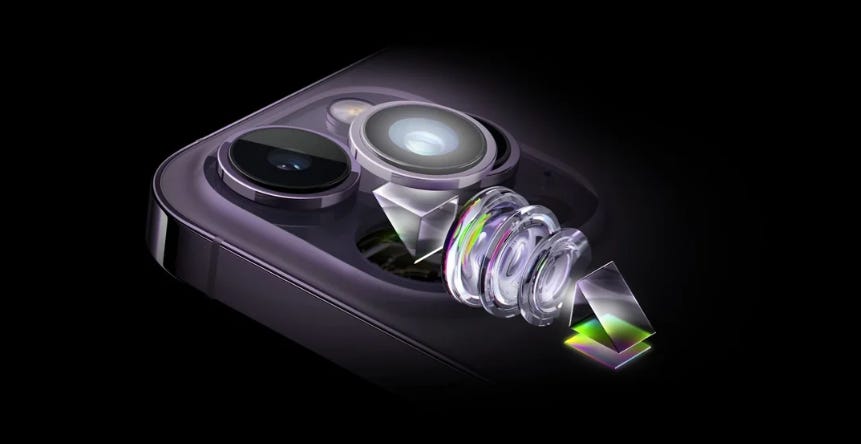
Metasurfacesandmetalensesfundamentally rewrite this paradigm. Instead of a thick lens element, they pattern a layer of subwavelength structures—dense arrays ofnanopillarsornanofins—on an ultra-thin film. Each nanostructure functions like a “pixelated phase-delay element,” precisely tuning the phase, amplitude, and polarization of transmitted light through geometric dimensions, shape, and refractive index. Once patterned on a wafer, a single 12-inch wafer can contain thousands or even tens of thousands of metalenses—our slide illustrates 5,000 metalenses on one wafer, each roughly 1 mm in diameter, with a 20,000× magnification revealing the dense nanopillar array.
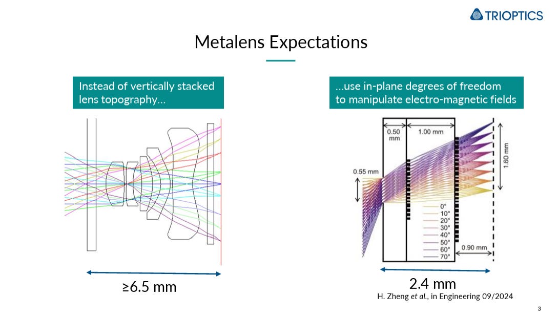
From a system-level viewpoint,meta-opticsintroduces several key differentiators:
Ultra-thin, planar integration:Achieves effective focal length comparable to high-NA refractive lenses, yet with a thickness of only a few hundred nanometers to a few micrometers. It can be directly integrated onto chips or packages.
High design freedom:Each nano-unit independently encodes phase and polarization response, enabling non-traditional wavefronts such as vortex beams or holographic patterns.
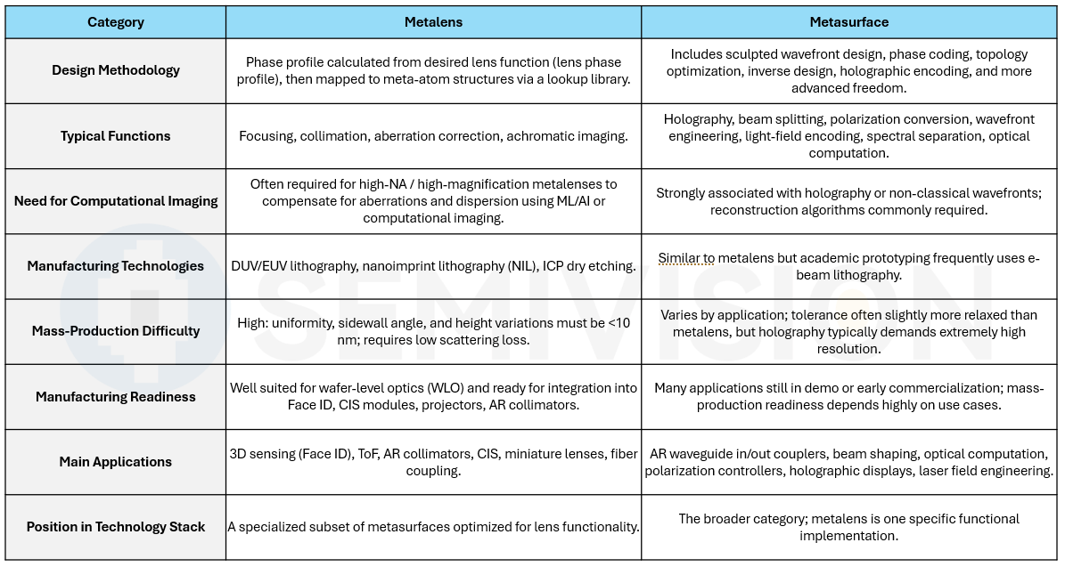
Semiconductor-process compatible:Manufacturable using DUV/EUV lithography, nano-imprint lithography, and dry etching, allowing high-volume replication on CMOS or glass substrates.

The theoretical foundation of this generation of meta-optics traces back to 2011, when Nanfang Yu from Harvard’s Capasso Group introduced the concept of phase discontinuities, a breakthrough in metasurface-based optical control. The key idea is to use engineered micro-structures to induce abrupt phase shifts at an interface, breaking through the constraints of traditional refractive optics and enabling entirely new forms of wavefront manipulation—such as generating vortex beams. This seminal work was published inScience, and the subsequent development of a complete “flat-optics” design framework by the Capasso group laid the foundation for today’s metalens technology.

2025年9月4日
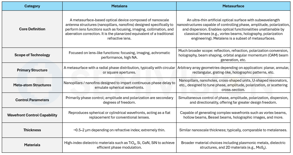
Metalens is a metasurface specifically designed for imaging and focusing, using metasurface technology to realize a flat, ultra-thin lens.
Metasurface, by contrast, is a broader concept—of which metalens is only one application.
The choice of materials for metalenses and metasurfaces is not determined solely by refractive index; instead, it is jointly governed by optical efficiency, spectral absorption, process maturity, achievable aspect ratio of nanostructures, sidewall roughness tolerance, and compatibility with CMOS and WLO (wafer-level optics) manufacturing.
For metalenses intended for commercial production, materials must satisfythree essential requirements: high refractive index × low absorption × manufacturability.
As a result, nearly all commercial metalenses today aredielectric metasurfaces, with different material families selected for different spectral bands.
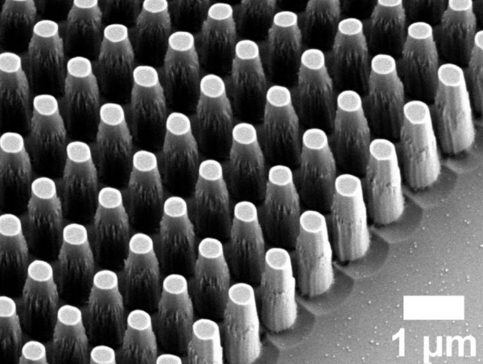
In the visible range, where wavelengths are short, absorption is high, and scattering sensitivity increases, materials face the strictest constraints.TiO₂ (titanium dioxide)is currently the most widely used choice, with refractive index n≈2.4, extremely low absorption, good compatibility with glass substrates, and suitability for NIL or DUV lithography to replicate high-resolution nanopillar arrays on large wafers.GaN (gallium nitride), with its wide bandgap, high optical damage threshold, and refractive index comparable to TiO₂, has also emerged as a key material for high-efficiency visible metalenses; however, GaN processing is more expensive and requires MOCVD and specific substrates, making it more suitable for high-end optics or high-power laser applications.
Meanwhile,SiN (silicon nitride), despite its lower refractive index (n≈2.0) and thus reduced ability to achieve high NA compared with TiO₂ or GaN, is highly CMOS-compatible, exhibits low stress, and offers excellent control of film thickness. It therefore plays an important role in pixel-level metasurfaces for CIS (CMOS image sensors), particularly in applications requiring low crosstalk, light-field redistribution, and wavelength selectivity.
In the NIR and IR wavelengths (e.g., 850 nm, 940 nm, 1550 nm),silicon (Si)—which suffers from severe absorption in the visible but is very low-loss beyond NIR, with refractive index as high as 3.4—becomes the dominant material for NIR metalenses used in Face ID, ToF, depth sensing, and fiber-coupling applications.
Overall, the material foundation of metalenses must be built onhigh-index dielectric metasurfaces, rather than metals. Although metals can support plasmonic resonances and extremely thin structures in the visible regime, they suffer from very high absorption and struggle to exceed ~20% efficiency—making them unsuitable for commercial imaging-grade metalenses.
Metasurfaces, on the other hand, span a much broader material space. In addition to dielectric materials such as TiO₂, GaN, Si, and SiN, they also include plasmonic metals (Au, Ag, Al), 2D materials (graphene, MoS₂), and silicon–organic hybrid (SOH) structures. These are used for polarization conversion, beam shaping, holography, modulators, and reconfigurable metasurfaces—where the key requirement is determined by functional goals rather than imaging efficiency.
Thus, commercial metalenses converge toward “dielectric metasurfaces with high index and low loss,” whereas research metasurfaces exhibit a “multi-material, multi-physics” diversity.
In summary, materials are not accessories to metalens and metasurface design—they are the foundation of their physical performance and industrial feasibility. TiO₂ and GaN define the upper limits of visible-light efficiency; Si determines the practicality of NIR and IR markets; SiN balances CMOS compatibility with optical flexibility; and plasmonic and 2D materials extend metasurfaces into dynamic, tunable, and non-classical wavefront engineering. Together, these form the complete material ecosystem of today’s meta-optics landscape.
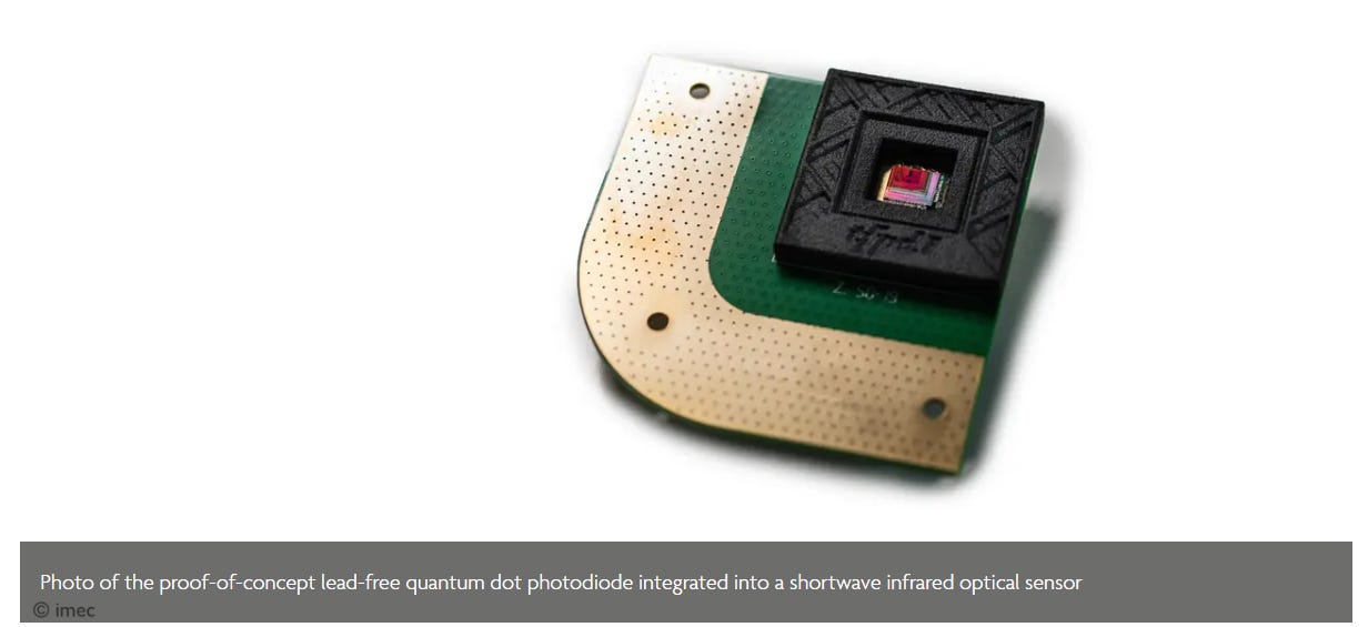
2025 IEDM : Metasurface cointegartion with Colloidal Quantum Dot Photodiodes Enabling Facile Spectral Sensors
At the2025 IEDM,we saw imec, for the first time, successfully integrate metasurface (meta-optic) technology with quantum-dot photodiodes (QDPDs) within the same CMOS process platform. The core idea of this paper is actually very straightforward: using a standard 300 mm wafer process, imec embeds a nanostructured metasurface capable of precise wavefront control directly into the quantum-dot microcavity absorption layer.

This approach enables SWIR spectral sensors—traditionally dependent on expensive materials such as InGaAs, bulky optical filters, or high-temperature processes—to be manufactured directly on CMOS withlow cost, high scalability, and pixel-level miniaturization.
Imec and partners unveil SWIR sensor with lead-free quantum dot photodiodes
More importantly, the metasurface is not merely an optical element—it simultaneously fulfillsoptical manipulationandelectrical conduction, allowing each pixel to fine-tune its absorption wavelength through nanoscale refractive-index engineering. This architecture allows a QDPD to cover a tunable spectral window from1230 to 1550 nmusing a single material stack, marking the first time that an optical element enters mainstream semiconductor manufacturing in a trulymeta-opticfashion.
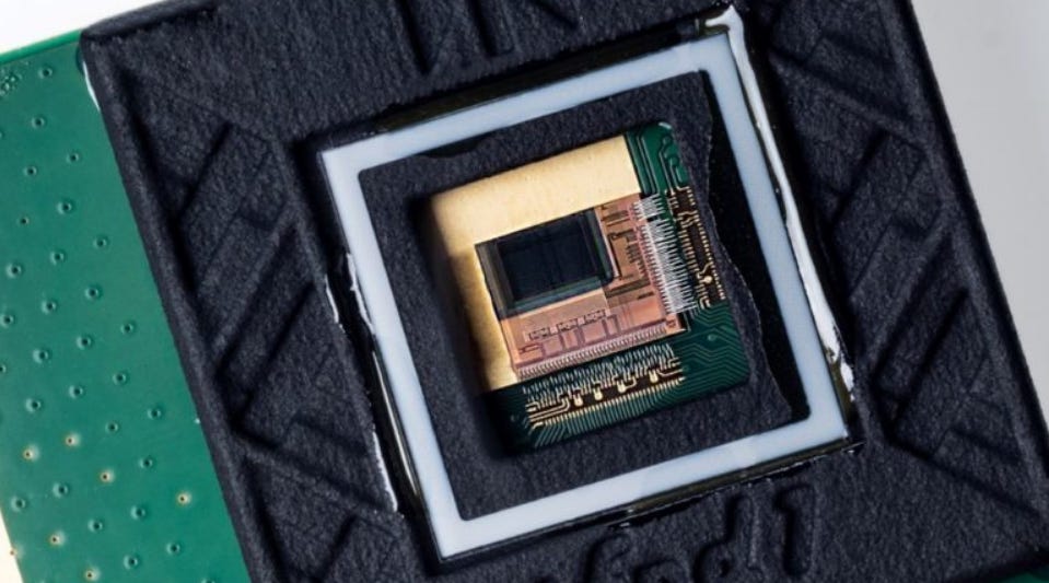
For quantum technologies, this breakthrough implies that future quantum light sources, quantum detectors, and quantum imaging architectures may be built on-chip using similar meta-optic strategies. The implications span from spectral imaging to fully integrated quantum-photonics platforms, opening a new stage of convergence between optics and quantum systems.

From CMOS-Compatible Metasurfaces to the Quantum Photonic Frontier — An Optical Revolution Now Underway
As short-wave infrared (SWIR) imaging becomes essential for automated inspection, precision agriculture, biomedical diagnostics, and environmental monitoring, the industry has encountered a persistent and unavoidable bottleneck: although traditional InGaAs sensors and thin-film Fabry–Pérot filters offer excellent performance, they are expensive, process-intensive, and incompatible with CMOS. As a result, SWIR spectral imaging has struggled to achieve the same widespread adoption seen in visible-light imaging.

The paper presented atIEDM 2025introduces a breakthrough solution at precisely this inflection point—using aCMOS-compatible metasurfacetogether with acolloidal quantum-dot photodiode (QDPD)to form a microcavity structure. With a single PbS quantum-dot material plus refractive-index engineering via nanopillars, the device achieves continuously tunable, narrow-band absorption responses between1230 and 1550 nm, comparable to a Fabry–Pérot filter.
Crucially, this entire spectral-selective, multi-pixel, high-resolution SWIR imaging capability is implementedinside a standard 300 mm wafer flow, using dual-damascene Cu interconnects, CMP, and DUV lithography—without any exotic materials or high-temperature processing.
In this architecture, the metasurface is no longer merely an “optical pattern.” It is ameta-optic device that provides both optical wavefront control and full electrical connectivityrequired for CMOS imagers, operating directly at the pixel level. Combined with the broadband absorption characteristics of quantum dots, this new meta-optic + QDPD design demonstrates an EQE of 40% over 1230–1550 nm, while also offering manufacturability, low cost, small pixel pitch (<10 μm), and high resolution (>1 MP). This opens the possibility for SWIR sensing to break free from its historically niche, high-cost market and scale into true commercial deployment.
But more importantly, this CMOS-integrated metasurface platform extends far beyondspectral imaging. Because metasurfaces can precisely manipulate phase, amplitude, polarization, and optical modes at subwavelength scales—while simultaneously enhancing light–matter interactions inside a microcavity—it is naturally suited for integration with quantum photonics. Such structures can:
Enhance single-photon emission rates of quantum dots or defect centers via Purcell effects
Serve as ultra-efficient coupling interfaces for quantum light sources and detectors
Generate non-classical optical fields with structured topology (OAM, Bessel beams)
Enable on-chip quantum imaging, quantum ghost imaging, quantum LiDAR
Provide a path toward quantum communication and quantum information processing
The paper’s demonstration of tunable-index meta-cavities, large-scale nanostructures, and full CMOS compatibility suggests that future quantum-photonic devices will no longer be confined to optical tables. Instead, they may adoptpixel-array architectures, multi-mode optical control, and full-wafer integration, entering the industrial ecosystem transformed by CMOS.
This is not merely a leap forward for SWIR imaging—it marks the beginning of a new era where optics and quantum technologies intersect and prepare to co-evolve into the next generation of sensing and computing architectures.
From Meta-Optics × QDPD to a Quantized Light-Field Control Platform
The most groundbreaking aspect of this work is that it does not merely demonstrate a standalone metasurface; rather, it fully integratesmeta-opticsandcolloidal quantum-dot photodiodes (QDPDs)within a single CMOS process flow to create a microcavity-enabled, spectrally tunable, and mass-producible SWIR spectral-sensing platform.

The metasurface is patterned usingDUV (deep-UV) lithographyto etch nanoscale Si/SiO₂ pillar structures into amorphous silicon. By exploiting the effective-index variation induced by pillar diameter, the design tunes the microcavity’s resonance wavelength, while a single PbS quantum-dot absorption layer provides continuous spectral tuning from1230 to 1550 nm, demonstrating the characteristic meta-optics advantage of“single material, multiple tunable functions.”

More importantly, the metasurface serves bothoptical and electricalroles. A damascene Cu layer beneath acts simultaneously as a mirror and an electrode; the Si/SiO₂ pillars form the meta-pattern; and Cu vias together with an ITO contact are fabricated above the metasurface—allowing wavefront (or resonance) control and electrical conduction to be co-implemented entirely within a CMOS-compatible process.
This electro-optical co-designed structure allows the microcavity QDPD to not only control its absorption spectrum through nanoscale photonic engineering but also maintain the full routing capability required for large-area imaging arrays. As a result, SWIR spectral imaging—once constrained by bulky systems or expensive materials such as Fabry–Pérot filters and InGaAs FPAs—can now be realized as awafer-scale, pixel-tunable, and substantially lower-cost CMOS-compatible technology.
The Next Step for Metasurface–Quantum Integration — From Light-Field Engineering to Quantum Signal Enhancement
When a metasurface can precisely control the spatial distribution, phase, and cavity modes of light, it naturally becomes an ideal platform for integrating quantum photonics. The device architecture demonstrated in this paper provides the key practical conditions needed for quantum technologies to transition toward real deployment: nanoscale light-field control, wafer-foundry manufacturability, and pixel-level integration of quantum absorbers (QDs).
QDPDs themselves arequantum-confined absorberswhose carrier absorption behavior and density of states are intrinsically determined by their nanoscale structure. Introducing metasurfaces into quantum applications enables them to function as:
Rapid in-/out-couplers for quantum light sources:
Using microcavity Purcell enhancement to boost single-photon emission rates from quantum dots or defect centers (e.g., InAs QDs, Er-doped SiN, 2D materials).
Efficiency enhancers for quantum detectors:
Meta-cavity–based field reinforcement improves absorption and mode confinement, making single photons or weak optical signals more effectively coupled into photodiodes, SPADs, or SNSPDs.
On-chip shapers of quantum optical states:
Metasurfaces can generate optical modes with OAM, spatial entanglement, or controlled polarization, enabling quantum imaging, ghost imaging, or free-space quantum communication.
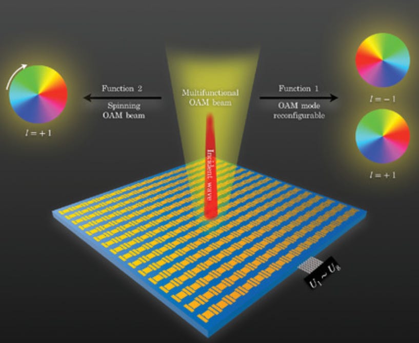
The paper demonstrates that tuning the effective refractive index via pillar diameter enables the QD absorption spectrum to shift from 1230 nm to 1550 nm, forming the foundation for multi-band quantum photonic devices. And because these meta-patterns can be replicated at scale in a CMOS process, it suggests that quantum photonics may evolve from laboratory setups toward array-based, widely deployable, and CMOS-fabricated industrial platforms.
In other words, this research does more than propose a new spectral-sensing scheme—it outlines a practical industrial roadmap for moving quantum photonics from thesystem levelto thepixel level:
metasurfaces for light-field engineering,
QDPDs for low-cost quantum absorption,
CMOS for high-volume fabrication.
Together, these elements form the blueprint for futurequantum imaging, quantum sensing, and quantum communication chips.

First electronic-photonic quantum chip manufactured in commercial foundry
Operating Mechanisms of Metalenses: Phase, Polarization, and Chromatic Dispersion
We can compare a metalens directly with a refractive lens: a traditional lens accumulates phase through the material refractive index and curved geometry, whereas a metalens constructs the same wavefront on a flat surface by engineering the phase response of subwavelength nanostructures.
Phase
The core of metalens design is thephase profile. Designers first define the desired phase distribution on the flat surface (for example, a parabolic phase profile needed for aberration-free focusing), then discretize this continuous phase into a grid. Each grid cell is assigned a nanopillar that provides the required phase delay.

The classic work by Khorasaninejad et al. (Science, 2016) demonstrated this principle using high–aspect-ratio TiO₂ nanofins to achieve NA = 0.8 focusing at 405/532/660 nm—near the diffraction limit—showing that a planar structure can indeed reach high numerical aperture focusing.
Polarization
Metasurfaces can combine geometric phase (Pancharatnam–Berry phase) with propagation phase arising from refractive-index contrast. This enables the creation of polarization-sensitive or polarization-insensitive metalenses.
Subsequent research has demonstrated metalenses in the visible regime that function for arbitrary polarization states, mitigating polarization dependence in practical imaging systems.

Chromatic Dispersion and Bandwidth (Dispersion / Achromatism)
Because metalenses are fundamentally diffractive optical elements, their dispersion is typically much stronger than that of refractive lenses, making broadband or achromatic operation extremely challenging.
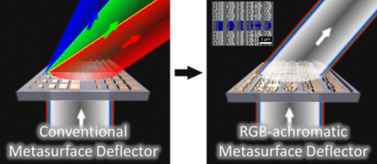
Recently, however, through multilayer designs, multi-resonant meta-atoms, and computational-imaging–assisted correction, researchers have achieved broadband achromatic metalenses in the visible, including devices capable of RGB or full-visible-spectrum imaging.

Applications: Metasurfaces / Nano-Light Pillars on CMOS Image Sensors
Most readers are familiar with conventional CIS architecture, so here we begin discussingCMOS image sensors (CIS) using metasurface-like structures, focusing on the nano-light pillars (NLP) concept recently presented by VisEra / AuthenX at IEDM.
What is CIS?

A CMOS Image Sensor, or CIS, is a semiconductor device that functions much like the retina of the human eye—it captures incoming light and converts it into electrical signals that can be processed by electronic systems.
In the human visual system, light enters through the cornea and lens, reaches the retina, and is transformed into neural signals that travel to the brain.
A CIS performs an analogous role in digital imaging. Light passes through a camera lens and strikes the sensor surface, where millions of tiny photodiodes convert it into electrical signals. These signals are then sent to downstream processors that reconstruct the final image.
In other words, the CIS acts as the“electronic eye”that enables smartphones, cameras, vehicles, and countless other systems to see the world.
Structural Concept
Traditional CIS places a micro-lens above each pixel to concentrate incoming light. However, when pixel pitch shrinks to 0.8 μm and below, micro-lens size becomes severely constrained, making it difficult to simultaneously maintain angular tolerance and high quantum efficiency (QE).
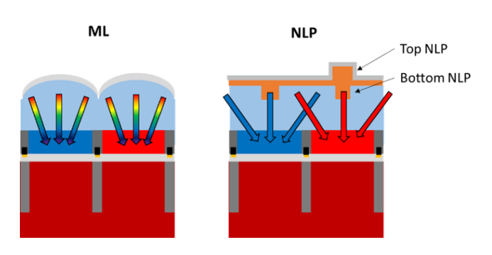
The NLP concept replaces the traditional single micro-lens with anano-pillar array, effectively forming a metasurface-like structure above each pixel. These nano-light pillars guide light more efficiently into the photodiode.
Optical Performance
For0.8 μm pixels, NLP improves QE by:
~40%for blue pixels
~16%for green pixels
compared with conventional micro-lens CIS.
Under20 luxlow-light conditions, brightness SNR improves by~1.16 dB, while preserving color accuracy.

Key Technical Factors
Theaspect ratio,sidewall roughness, andrefractive-index profileof the nano-pillars determine light guiding efficiency.
The structure must remain compatible with existingcolor filter arrays (RGB/CMY)and BEOL processes without introducing excessive stress or yield loss.
This work corresponds to the 2023 conference paper from VisEra,
“CMOS image sensor with nano light pillars for optical performance enhancement”by C. Wang et al.

TSMC 2025 IEMD :0.43 µm Quad-Photodiode CMOS Image Sensor by 3-Wafer-Stacking and Dual-Backside DTI
TSMC’s 2025 IEDM Contribution: Toward the Next Pixel-Scaling Frontier
AtIEDM 2025, TSMC further pushed CIS scaling with the paper:
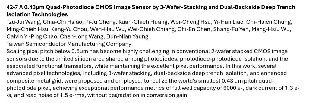
“0.43 µm Quad-Photodiode CMOS Image Sensor by 3-Wafer-Stacking and Dual-Backside DTI.”
This result is not merely about “making smaller pixels”—it reflects a broader transformation in CIS technology:
image sensing is evolving from asingle-chip engineering probleminto afour-pillar system engineering challengeinvolving:
Optics
Process technology
Stacking architecture
Nano-optical elements
Two Technology Pathways Converging Toward the Same Goal
Over the past decade, two parallel approaches have been advancing one shared objective—
capturing light more effectively, completely, and precisely:
- Chip-side innovations
3-wafer stacking, Dual-BDTI, Cu-Cu hybrid bonding, etc.
→ Address pixel shrinkage, crosstalk, and rising electronic noise.
- Optics-side innovations
Meta-lens / micro-lens using nanostructures to reshape light
→ Address light-collection efficiency, angular response, chromatic aberration, and focus accuracy.
Thus, CIS is no longer just “converting light into electrons.”
It is becoming afull opto-electronic platform:
Theupper layeruses optical structures (meta-optics) to improve light utilization.
Thelower layersuse stacking and isolation technologies to improve electrical signal integrity.

TSMC’s 3-wafer-stacked CIS as the Perfect Example
At a pixel size of0.43 μm, light itself behaves close to optical-wave scales.
Therefore,guidingthe light is now just as important asreadingthe electrons.
At this scale, meta-lenses, micro-lenses, color filters, phase shifters, and CMG+ optical elements must be co-designed together with BDTI, front-side / back-side isolation, hybrid bonding, and 3D stacking.
In other words, the future of CIS is no longer a separation of
“optics outside, chip inside.”
It is a fully integratedphotonic–electronic co-designsystem.

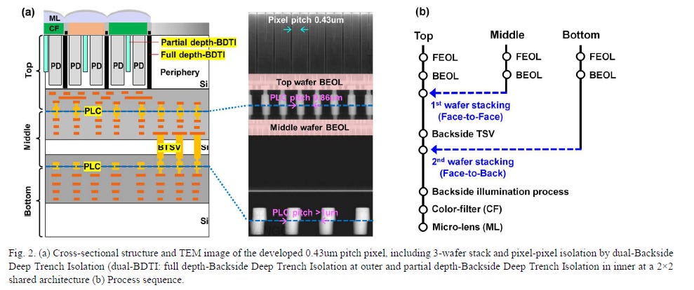
At the 2025 IEDM conference, TSMC presented the paper “A 0.43 µm Quad-Photodiode CMOS Image Sensor by 3-Wafer-Stacking and Dual-Backside Deep Trench Isolation Technologies.” The work focuses on distributing the photodiode, pixel transistors, and backend image-processing circuitry across three separate wafers, overcoming the fundamental sensitivity bottlenecks that arise as pixel sizes shrink. The concept had previously appeared in a simplified form at TSMC’s TechForum, but the IEDM paper is the first to disclose the actual device architecture, process details, and measurement results, effectively establishing the baseline implementation of a triple-stacked CIS.
Building upon this introduction, the current article will analyze the physical and process mechanisms behind the three-chip stack and compare TSMC’s approach with the latest stacked CIS architectures from Sony and Samsung.
The key points of TSMC’s IEDM paper are:
Pixel scaling has reached a regime below 0.5 µm, where further shrinkage severely degrades image quality. TSMC’s solution is to disaggregate the CIS into three optimized layers—a photodiode layer, a pixel-circuit layer, and an image-processing layer—each fabricated with the most suitable process technology. The three wafers are then integrated using ultra-fine-pitch Cu-to-Cu hybrid bonding.
At the same time, Dual-BDTI (dual backside deep trench isolation) and CMG+ technologies are introduced to preserve, and even enhance, imaging performance despite aggressive pixel scaling.
As a result, TSMC achieves a leap from 0.6 µm to 0.43 µm pixels with no deterioration in image quality—in fact, with measurable improvement.
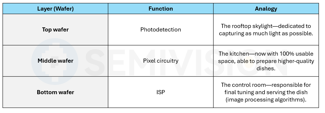
If we use a simple analogy to illustrate triple-stacking:
Think of a CIS as a restaurant. Historically, it only had two floors (sensing + circuitry). But the “kitchen” was too cramped—the middle floor was occupied by TSVs—so the restaurant could no longer improve the quality of its dishes (image performance). The three-layer architecture essentially expands the building, freeing space and enabling a higher-performance system.
The Inevitable Trend Toward Pixel Miniaturization and Stacking
Smartphone cameras have pushed pixel sizes from 1 µm down to below 0.5 µm. However, in the conventionaltwo-layer back-illuminated CMOS image sensor (CIS)architecture, the silicon area available to each pixel is fundamentally constrained, leading to three major bottlenecks:
Shrinking photodiodes reduce saturation capacity.
When pixel pitch falls below 0.5 µm, the active photo-collection area becomes so small that the full-well capacity (FWC) drops significantly.
Pixel transistors consume a large portion of silicon area.
In the traditional 2-wafer architecture, MOS devices such as the source follower (SF), reset switch (RST), and select switch (SEL) coexist with the photodiode on the same die. This co-location increasescrosstalk and noise.
Through-silicon vias (TSVs) and deep contacts limit the usable silicon area in the middle layer.
To route signals from the sensing layer to backend circuitry, TSVs must pass through the substrate. These vias occupy substantial area and constrain functional density within the die.
As a result, simply shrinking pixels can no longer balance resolution and sensitivity. TSMC’s triple-wafer stacking introduces physical partitioning and heterogeneous bonding to regain design freedom for ultra-small pixels. At the same time, Dual-BDTI (dual backside deep trench isolation) enhances pixel-to-pixel isolation, while CMG+ (enhanced metal grid) improves optical efficiency.
The following sections detail each of these enabling technologies.
Technology Evolution of CMOS Image Sensors (CIS) and the Era of Three-Layer Stacking
From FSI to BSI: Evolution of Optical Paths in Image Sensors
Early CMOS image sensors primarily adopted afront-side illumination (FSI)structure, where light had to pass through metal wiring layers and other circuit layers before reaching the photodiode. This architecture worked reasonably well for pixel sizes above 1.12 µm, but as pixels shrank, the proportion of metal wiring remained almost unchanged. This reduced the optical aperture, introduced strong diffraction and dispersion effects, and increased scattering or absorption of photons when passing through metal—ultimately lowering quantum efficiency and causing pixel-to-pixel optical crosstalk.
Back-side illumination (BSI)technology entered mainstream smartphone CIS around 2011. In BSI, the sensor is flipped so light directly reaches the photodiode from the backside; the photodiode and microlens sit above the metal wiring. This eliminates metal blockage, enables pixel sizes of ≤1.12 µm, and improves resolution and low-light sensitivity. To suppress crosstalk in BSI arrays, optical isolation and enhancement structures such as Backside Deep Trench Isolation (BDTI), W-Grid, and Air-Grid were developed.
Emergence of 3D-Stacked CIS
As smartphone demand grew for higher resolution, smaller modules, and faster imaging, it became difficult to integrate all required functions on a single wafer. In 2012, Sony introduced the world’s firsttwo-layer stacked CIS, combining a BSI pixel wafer with an image-processing logic wafer usingTSVs (Through-Silicon Vias)and oxide bonding. This allowed each wafer to be manufactured using an optimal process node, improving image quality and reducing noise.
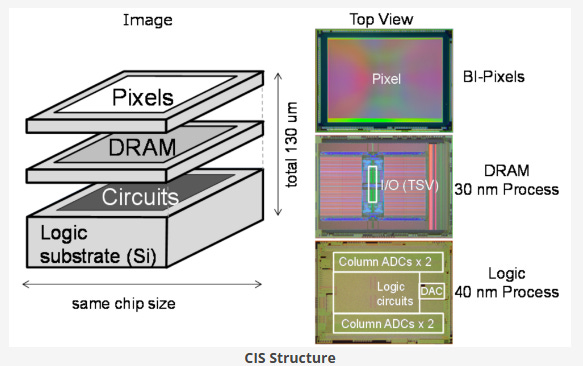
In 2017, Sony unveiled athree-layer stacked image sensor:
Top layer:BSI pixel array
Middle layer:DRAM cache
Bottom layer:Image signal processor (ISP)
This device adoptedhybrid bondinginstead of traditional TSVs. The motivation for three-layer stacking includes enabling new functions, reducing module size, increasing flexibility in process selection, and optimizing each layer independently.
Hybrid Bonding and Its Role in Three-Layer CIS

Hybrid bonding is a newer chip-stacking technology that creates direct copper-to-copper contacts between wafers to serve as both electrical and mechanical interconnects. Compared with TSVs or solder bump interconnects, hybrid bonding achieves micron-scale bonding pitch, dramatically increasing vertical interconnect density and bandwidth.
The industry has already adopted this method in high-performance designs—for example,AMD’s 3D V-Cacheuses TSMC’s copper hybrid bonding to stack cache directly on a compute die, achieving near-monolithic performance and power efficiency.
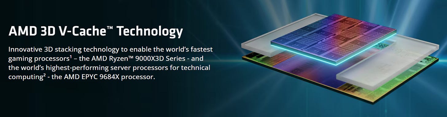
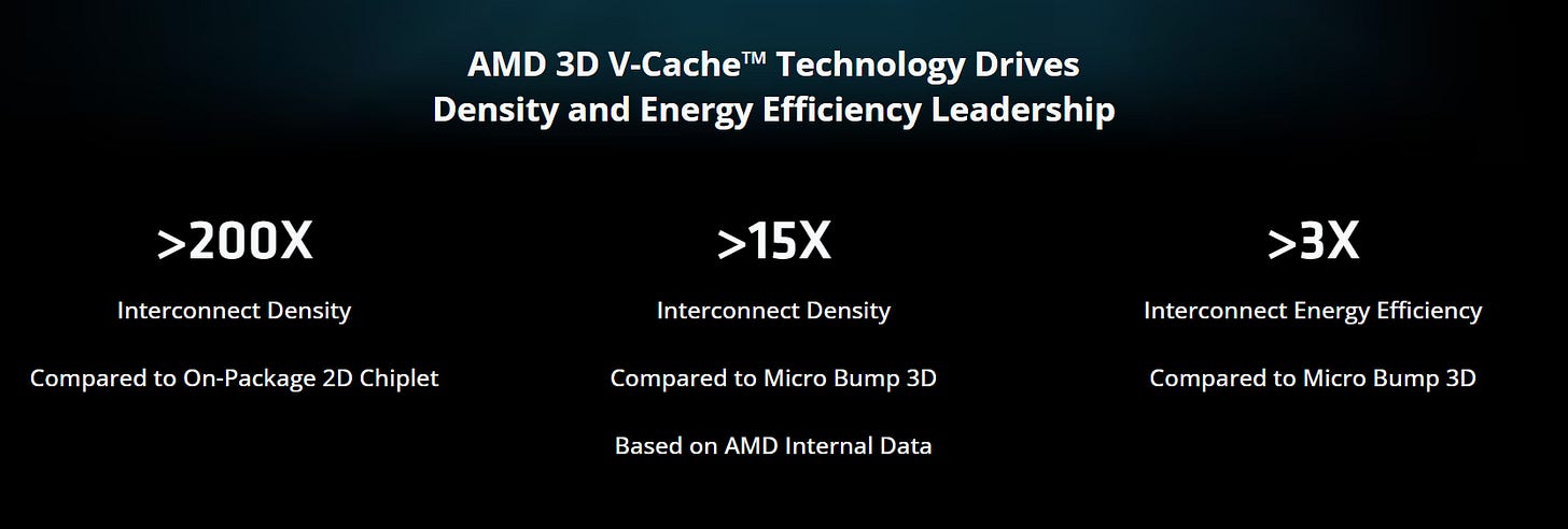
Today, hybrid bonding is primarily used in high-end applications: while costly, it enables smaller form factors, higher throughput, and far superior interconnect density, making it an essential technology for next-generation 3D-stacked CIS.
Three-Layer Stacked CIS: Architecture, Hybrid Bonding, and the Path Toward Sub-0.5 μm Pixel Scaling
Top Layer Chip:
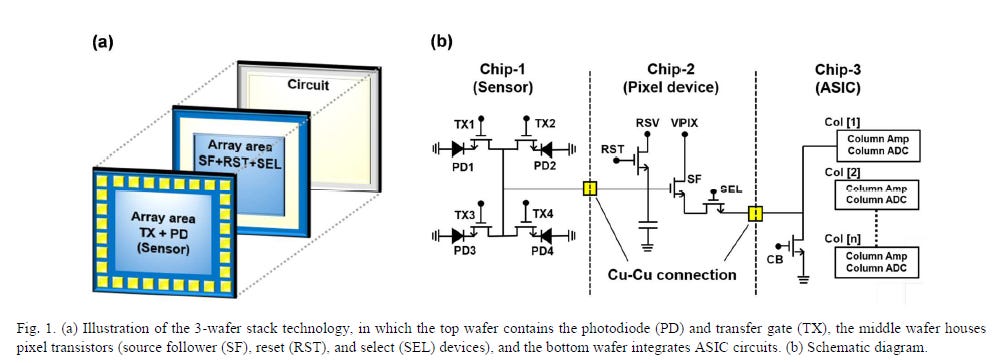
Contains the photodiode (PD) and transfer gate (TX). Since it performs only photo-sensing, it can use materials and thermal processes optimized for photodetectors. This layer adopts a backside-illuminated structure, and both FEOL and BEOL are optimized for optical performance.
Middle Layer Chip:
Hosts pixel transistors such as the source follower, reset, and selection switches. It is connected to the top layer viaface-to-face Cu-Cu hybrid bonding, eliminating the need for through-silicon vias (TSVs). As a result, nearly100% of the silicon areais available for transistor layout—one of the key advantages of three-layer designs over two-layer stacks.
Bottom Layer Chip:
Integrates row amplifiers, column ADCs, and ISP-related digital/analog circuits. Since it is unrelated to photo-sensing, a modern logic process node can be used, enabling higher compute density and lower power.
Central to the viability of this design ishybrid Cu-Cu bonding, which connects the top and middle layers at a pitch of 0.86 µm. Unlike TSV-based approaches, hybrid bonding requires no deep vias, imposes negligible parasitic loading, and keeps nearly 100% of the silicon active in the middle layer. Reliability data from TSMC shows near-perfect connection yield across 10,000 serially linked pads, and the technology remains stable even when scaled to 0.6 µm pitch. Signals traveling downward to the logic wafer pass through backside TSVs located entirely within logic areas, avoiding any disturbance to the pixel array. This combination of hybrid bonding and backside TSVs offers a finer-pitch, higher-yield alternative to earlier multilayer CIS structures and allows true per-pixel vertical connectivity.
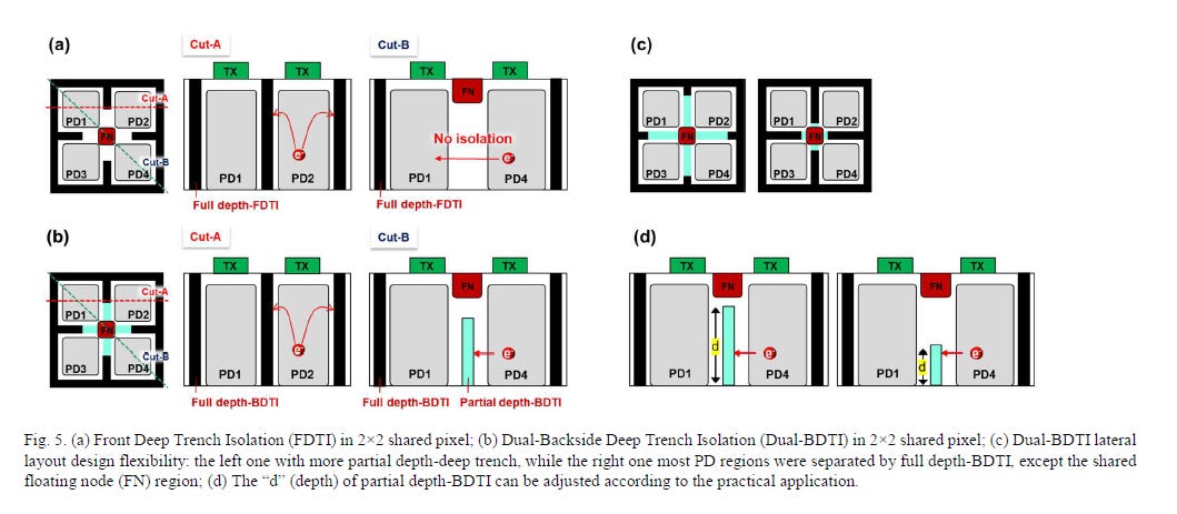
Another key innovation introduced in the work isdual backside deep trench isolation (dual-BDTI), designed to prevent charge spillover from saturated pixels. Outer 2×2 pixel groups use full-depth trenches for complete isolation, while the inner shared region uses partial-depth trenches that allow the four shared pixels to maintain a common floating diffusion node. The depth and width of the shallow trenches can be tuned independently, enabling both strong isolation and efficient charge sharing. This structure plays a critical role in scaling pixel pitch from 0.8 µm to 0.6 µm without degrading FWC, and it remains effective even at the 0.43-µm scale.
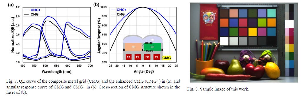
Optical enhancements further strengthen the design. TSMC employs a refined composite metal grid (CMG+) with thinner metal lines and low-index materials to better confine optical beams and reduce absorption. These improvements raise QE by roughly 10% with only minimal increase in crosstalk, demonstrating that optical performance can still be improved even as pixels become extremely small.
The performance metrics of the 0.43-µm three-layer Quad-PD pixel underscore the maturity of the approach. At 60 °C, the dark current measures 1.3 e⁻/s, read noise reaches 1.5 e⁻ rms, and the conversion gain remains close to 1.01 a.u.—values comparable to or better than state-of-the-art two-layer sensors. In other words, the aggressive scaling and additional stacking do not introduce noticeable performance penalties.
The broader significance of three-layer CIS goes beyond pixel scaling. By separating sensing, analog processing, and logic into different wafers, the architecture opens the door to new functional integration paradigms. Sony has already demonstrated three-layer sensors that incorporate DRAM or deep neural network accelerators on the logic wafer, enabling high-speed capture and on-sensor AI inference. Because the bottom layer sits closest to the package, it can dissipate heat more efficiently, making it suitable for power-hungry logic. Meanwhile, internal data movement within the stack reduces the need for high-bandwidth off-chip I/O, lowering overall system power.

TSMC’s most advanced CMOS Image Sensor (CIS) technology enables stacking CIS devices with special options, such as advanced image signal processor (ISP), near infrared (NIR) enhancement, and high-density capacitors. This cutting-edge CIS technology provides smarter, higher resolution IoT products with better high dynamic range (HDR) performance and lower power consumption.
Smart CIS-driven IoT applications are everywhere:
Smart doorbells in wireless home security systems use the Internet so that homeowners can interact with visitors from anywhere
Baby and pet monitor cameras connect to smartphones. Features include full-color night vision, watchdog mode with instant response, and event trigger recording
Interactive home assistances and home virtual reality (VR) trainer devices incorporate one or more image sensors
New CIS technology with improved NIR capability empowers emerging applications, such as smart locks and gate controls with 2D/3D facial recognition
Future Outlook of CIS Technology
From FSI → BSI → 2-layer → 3-layer stacking, CIS evolution is driven not only by resolution but by:
Higher optical efficiency
Lower noise
More integrated functions
Flexible process optimization
Hybrid bonding dramatically increases vertical interconnect density.
Future sensors are expected to integrate:
Image processing
Memory
AI inference engines
directly into the stacked structure, enabling edge computing and ultra-fast image pipelines. Simultaneously, optical innovations such as improved trench isolation and metal-grid engineering will continue to enhance QE and suppress crosstalk.

Sony was the earliest company to commercialize stacked CIS technology. Its first-generation stacked sensor, introduced in 2012, used avia-last TSV processto vertically stack the sensing chip and the logic chip. In 2021, Sony advanced this architecture by placing the pixel transistors on a dedicated wafer, creating atwo-layer transistor–pixel structure. This separation allows both the photodiode and pixel transistors to be individually optimized, and the saturated signal level can be roughly doubled compared with conventional sensors.
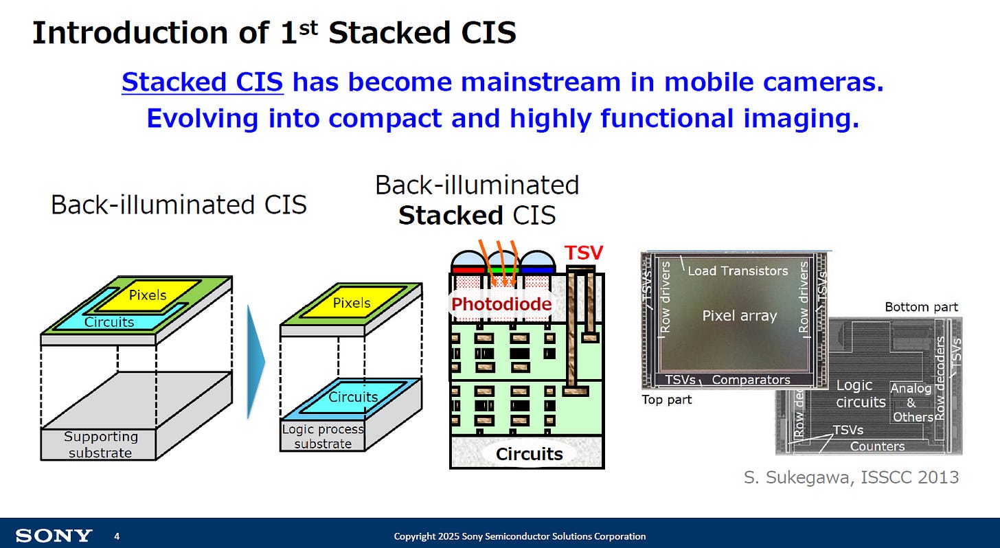
In its 2025 investor briefing, Sony revealed plans for athird layer, stacking a dedicated processor or memory die on top of the first two layers—for example, integrated DRAM or neural-network accelerators. According to Sony, adding a processing layer improves dynamic range, readout speed, and overall efficiency, and even enables new high-frame-rate video modes. However, increasing the number of layers does not inherently improve resolution, and designers must still avoid the reduction in full-well capacity that accompanies pixel scaling.

In summary, Sony’s multi-layer stacking strategy shares a conceptual foundation with TSMC’s approach: both emphasize separating the photodiode and pixel transistors into different layers and leveraging 3D stacking to add functional capability. The difference lies in focus. Sony prioritizes integrating DRAM or AI accelerators at the logic layer to enable advanced end-user features, while TSMC’s research concentrates on achieving high sensitivity, manufacturability, and small-pixel scalability. TSMC does not integrate memory or AI engines into the stack; instead, it focuses on process optimization and structural engineering for extremely small pixels.
Comparison with Samsung’s Latest CIS Technologies

Samsung’s high-resolution Isocell lineup continues to push pixel scaling forward, with mass production already at 0.64 µm (HP1) and development progressing toward 0.5 µm. Samsung first leveragedFront Deep Trench Isolation (FDTI)andbonded-wafer passivationto achieve both strong pixel isolation and sufficient photodiode volume.
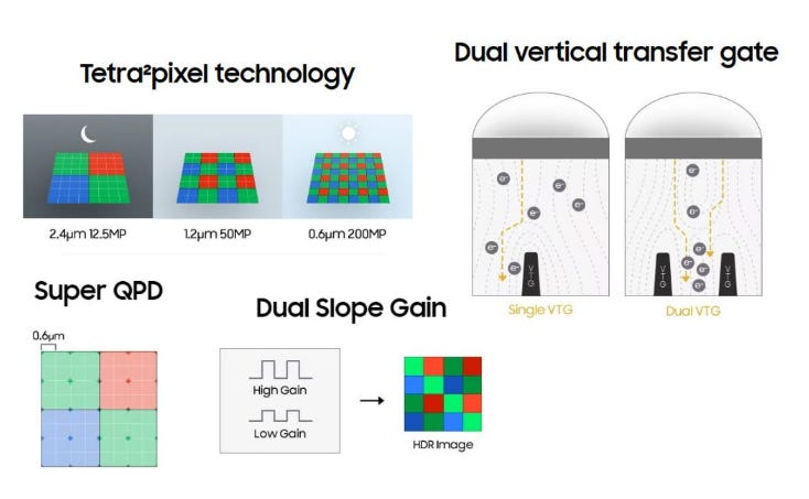
In 2023, Samsung introduced Dual Vertical Transfer Gate (D-VTG) technology, replacing the conventional single vertical transfer gate with two stacked gates and using PLAD (plasma-assisted doping) to shrink the pixel pitch to 0.64 µm while maintaining an FWC of 6000 e⁻. D-VTG places the transfer gate structure beneath the photodiode, allowing the photodiode depth to increase, which improves both saturation capacity and quantum efficiency. Simulations show that reducing the spacing between the two transfer gates from 130 nm to 20 nm significantly accelerates charge transfer.
Samsung’s ISOCELL HP2 is the first 200-MP sensor to adopt D-VTG. Each pixel captures about 33% more electrons than previous 200-MP designs, and at the same operating voltage, FWC increases by roughly 66%. Random noise (RN), random telegraph signal (RTS), and thermal leakage remain comparable to single-gate architectures.
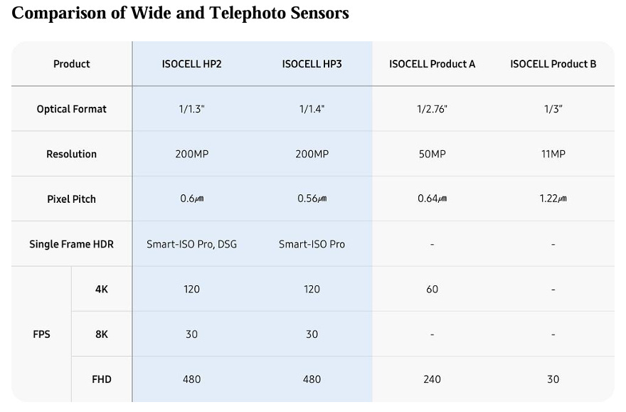
Samsung has not publicly announced or demonstrated athree-layer stacked CISarchitecture.
Its recent advancements focus on pixel-level device engineering (such as D-VTG and FDTI) rather than multilayer stacking, which differentiates its roadmap from Sony and TSMC.

TSMC’s three-chip stacking technology demonstrates that even when pixel size is reduced to 0.43 µm, high sensitivity and low noise can still be preserved through proper functional partitioning, hybrid bonding, and advanced deep-trench isolation. Dual-BDTI effectively resolves the crosstalk challenges inherent to 2×2 shared pixels, while the CMG+ optical refinements improve quantum efficiency by about 10% in small-pixel regimes. Compared with the stacking roadmaps of Sony and Samsung, TSMC places greater emphasis on manufacturable process baselines and reliability, laying the groundwork for eventually integrating additional capabilities such as memory or AI.
As the smart-image-sensor market accelerates, three-layer stacking offers a practical path toward combining ultra-high resolution with wide dynamic range. If future designs incorporate a neural-network processor or high-speed DRAM on the bottom layer—merging Sony’s processing-layer concept with Samsung’s vertical-gate innovations—they could enable the next generation of high-performance intelligent cameras.
CIS — CMOS Image Sensor
The image-sensing semiconductor used for photography — the light-sensitive chip inside every smartphone camera.
This is the focus of the research, aiming to improve image quality, shrink pixels, and reduce power consumption.
Pixel Pitch — Pixel Spacing
The size of one pixel.
Smaller pitch = more pixels in the same area = higher resolution.
TSMC shrinks pixel pitch to0.43 µm, currently the smallest demonstrated.
Photodiode (PD)
The part of the pixel that “receives light” and converts photons into electrical charge — like a tiny bucket for electrons.
Thetop wafercontains only PDs and uses processes optimized for sensitivity.
Quad-PD (QPD)
A pixel containing four photodiodes.
Improves autofocus, HDR, and low-light performance.
The paper uses a4-PD structure scaled to 0.43 µm.
Full-Well Capacity (FWC)
How much charge a pixel can hold before saturating.
Higher FWC → less overexposure, better HDR.
Even at extremely small size, TSMC maintains6000 e⁻, which is exceptionally hard to achieve.
Conversion Gain (CG)
Indicates how efficiently light is converted into voltage.
Higher CG → better low-light performance.
The design achievesCG = 1.01, comparable to larger pixels (very impressive).
Dark Current
Noise generated when the sensor is not exposed to light.
Lower dark current → cleaner images.
TSMC achieves1.3 e⁻/s, an industry-leading value.
Read Noise
Noise added during the readout process.
Lower read noise → cleaner shadows and night shots.
Measured at1.5 e⁻, world-class performance.
2-Wafer CIS — Two-Layer Stacked CIS
A sensor with just asensing layer + logic layer.
This traditional architecture hits a wall when trying to scale pixels smaller.
3-Wafer Stacking — Three-Layer CIS
Separatesphotodiode, pixel transistors, and ISPinto three wafers, each optimized independently.
TSMC’s key innovation enabling scaling below0.5 µm.
Top Wafer
Containsonly PDs.
Uses materials and thermal steps fully optimized for light sensing.
Middle Wafer
Contains allpixel transistors(RST, SF, SEL).
Utilizes100% of its silicon area, since no TSVs occupy space.
Bottom Wafer
ContainsISP, ADC, and control logic.
Can use advanced nodes (5 nm / 3 nm), improving imaging algorithms and efficiency.
Face-to-Face Bonding (F2F)
Two wafers bonded with their front sides facing each other.
Uses ultra-dense0.86 µm Cu-Cu contacts, enabling fast, dense connections between PD and pixel circuits.
Cu-Cu Hybrid Bonding
Dense copper-to-copper interconnects without solder bumps or TSVs.
Achievessub-micron interconnect pitch, essential for scaling to 0.4 µm.
TSV — Through-Silicon Via
A large, deep conductive via.
In 2-wafer CIS, TSVs take up valuable space and limit pixel scaling.
Backside TSV
TSVs placedonly on the bottom wafer, enabling three-layer output routing without consuming middle-wafer area.
Shared Pixel
Multiple pixels sharing certain transistors to save space.
TSMC uses2×2 sharing, reducing the floating-node capacitance (FN).
Floating Node (FN)
The node that holds the electrons.
Too large → lowers CG
Too small → increases crosstalk
Three-layer stacking helps reduce FN capacitance.
DTI — Deep Trench Isolation
Deep trenches between pixels to prevent electrical and optical leakage.
Dual-BDTI — Dual Backside Deep Trench Isolation
Shallow trenches inside, deep trenches outside:
→ Provides both strong isolation and 2×2-pixel sharing at the same time.
TSMC’s second major innovation solving traditional crosstalk problems.
CMG+ — Enhanced Composite Metal Grid
A specialized metal-grid optical structure that improves light-guiding efficiency.
Boosts QE by~10%, especially for high-angle light.
QE — Quantum Efficiency
How effectively pixels convert light into electrons.
Higher QE → better image quality.
CMG+ improves peak QE by nearly 10%.
ISP — Image Signal Processor
The “brain” that performs noise reduction, HDR, color processing, etc.
Placed on the bottom wafer using advanced logic nodes to boost performance.
Meta-lens × Three-Layer Stacked CIS: A New Imaging Architecture for the Coming Decade
The three-layer stacked CIS presented in TSMC’s IEDM paper represents more than just a pixel shrink to 0.43 µm—it marks the beginning of a new architectural era for image sensors. With the top wafer dedicated entirely to light sensing, the middle wafer housing all pixel transistors, and the bottom wafer functioning as the ISP “brain,” the combination of Dual-BDTI, CMG+, and hybrid Cu-Cu bonding enables both optical and electrical signals to be processed in their most optimized domains.
This stacked structure opens unprecedented integration opportunities formeta-lenses and micro-lenses:
Meta-lenses can be directly integrated on the Top Wafer, potentially forming pixel-level light-guiding structures.
Micro-lens arrays can be co-optimized with CMG+ and BDTI to improve high-angle light collection.
Metallic nanostructures (meta-gratings) can compensate for phase and chromatic issues that arise at 0.43-µm pixel pitch.
Future designs may evolve into a fully optical front-end + three-layer electrical back-end imaging SoC.
If traditional CIS progress was driven byshrink, the next phase will be driven by:
Optical field engineering (meta-optics)
3D chip stacking
Nano-photonics × electronics co-design (PIC–EIC integration)
New optical materialssuch as TFLN, SiN, TiO₂, and others
TSMC’s IEDM paper signals that once pixels enter thesub-0.5 µm era, optics and silicon will no longer be separable domains.
The future of image sensing is a photonic–electronic integration paradigm built uponMeta-lens × 3D CIS.
In other words:
Three-layer stacked CIS represents a breakthrough in electronic architecture,
while meta-lenses and micro-lenses represent a breakthrough in the optical domain.
Only by combining both can we reach the true end-game architecture for the next decade of imaging.
AR Glasses & Meta-Optics: Metalens × Waveguide × Metacoupler
Next, we shift focus to AR/AI glasses and near-eye display technologies.
Roles of meta-optical components in AR systems
Metaholograms: metasurfaces that generate holographic images for illumination or light-field modulation.
Metalenses: provide focusing or collimation, shaping the microdisplay output into parallel or engineered wavefronts.
Metacouplers: couple light in or out of waveguides, providing a next-generation alternative to traditional diffractive gratings.
These components can expand field of view (FOV), reduce chromatic aberration, and maintain transparency—critical for consumer AR devices. The review papers cited in the slides, such as Zeyang Liu et al. inAdvanced Photonics, provide detailed surveys of metasurface-enabled AR architectures.
Multifunctional metasurfaces
A notable paper inLight: Science & Applicationsdemonstrated multilayer, multiperturbation non-local metasurfaces capable of performingtransmission, reflection, and narrow-band focusing simultaneously. This is highly suited for AR glasses, where space is limited but functional requirements are complex.
Commercial AR glasses examples
Today’s AR devices—includingXREAL One Pro,Digilens ARGO, andMeta Ray-Ban—still primarily rely on geometric or refractive waveguide optics. However, these architectures face emerging bottlenecks in field-of-view, chromatic dispersion, and module thickness. Meta-optics may become the key next-generation enhancement:
Metalens arrays enabling pixel interlacing or image stitching to increase PPD within limited display resolution.
Metasurfaces improving waveguide coupling efficiency, reducing ghosting and dispersion.
SemiVision has covered AR applications extensively in past articles, so we will not elaborate further here.

2025年11月6日
Telecommunications: Metalens for 2D Fiber-Array Packaging
In the communications domain, as AI GPUs and hyperscale data centers drive demand for high-density optical interconnects, advanced optical interfaces are becoming critical. AI accelerators and switches increasingly depend on 2D fiber arrays tightly coupled with photonic integrated circuits (PICs).
Traditionally, spherical/aspherical lenses or GRIN optics are used for beam shaping and coupling, but they face challenges in pitch, alignment tolerance, and form factor.
Metalenses, by contrast, can performmulti-point focusing and wavefront control on a single flat surface, making them ideal for planar optical packaging. Metalenses can be fabricated directly onto FAU cover plates or glass substrates, reducing assembly tolerances and supporting detachable 2D fiber-array interfaces that simplify testing and repair. Early prototypes were demonstrated at Computex 2025.
The ultra-thin, planar nature of metalenses positions them as a key enabling technology for futuresilicon photonics and CPO (Co-Packaged Optics)architectures, improving fiber-coupling efficiency and reducing module volume.

International Metalens / Meta-Optics Solution Providers
Metalenz, Inc. (USA)
Metalenz is a leading pioneer inplanar metalens technology, originating from MIT. The company focuses on enabling large-scale commercial deployment of metasurface optics for consumer electronics, mobile 3D sensing, and automotive applications.
Its core innovation allows multiple optical functions—focusing, filtering, beam shaping—to be integrated into a single, flat metasurface, replacing complex multi-element lenses.
According to its official descriptions, Metalenz partners with major semiconductor manufacturers such as STMicroelectronics, enabling CMOS-compatible mass production, which allows meta-optics to be manufactured with the scalability and cost structure of semiconductor wafers.

NIL Technology (NILT) – Denmark—
NILT is one of Europe’s most advanced suppliers ofmeta-optics and flat-optics solutions, specializing in the design, nano-imprinting, and mass production of high-performance metalenses and metasurfaces.
Reports and company publications highlight that NILT’s metalenses achieve high transmission efficiency, precise wavefront control, and broad customizability. Their products cover visible, near-infrared, and broadband optical applications.
NILT’s proprietary nanoimprint technology enables high-volume, high-uniformity fabrication, and the company actively collaborates with AR/VR device makers, smartphone OEMs, and 3D sensing module suppliers.
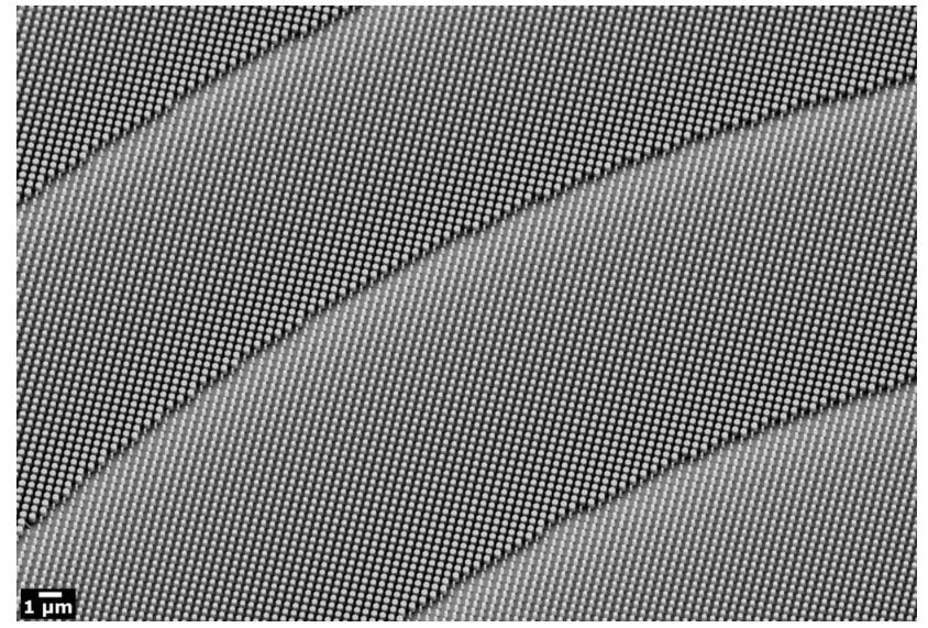
NIL Technology has a whole process chain under one roof for design, mastering, prototyping, testing and characterization, and manufacturing capabilities of meta optics.
Relevance to the Silicon Photonics / CPO Ecosystem
TSMC COUPE Platform—
Although not a component supplier, recent discussions indicate that TSMC’s COUPE (Compact Universal Photonic Engine) platform is exploring the use of metalenses as fiber-coupling and wavefront-engineering elements within CPO architectures. This includes concepts for integrating metalenses with 2D fiber-array units (FAUs) and future ultra-high-density optical interfaces.

2025年3月23日
Other Potential Academic–Industry Contributors
Several optics and photonics companies — for example,Hamamatsu Photonics— possess strong research backgrounds in photonics, nanophotonics, and metasurfaces. While they may not positionmetalens commercializationas a core business, their technical foundation in high-end optical communication, metrology, and sensing makes them potential collaborators or component suppliers in next-generation optical packaging.
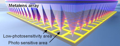
40 × 40 Metalens Array for Improved Silicon Photomultiplier Performance by Hamamatsu Photonics
Industry Trends and Significance
According to market reports, the metalens market for optical communications and fiber-coupling is growing rapidly, with expectations of double-digit CAGR over the next several years.
Key growth areas include:
fiber-optic communication
free-space optical links
interfaces for photonic integrated circuits (PICs)
The planar, wafer-level manufacturable nature of metalenses makes them highly attractive for silicon-photonics integration and CPO/FAU optical-interconnect packaging, where compactness, alignment tolerance, and scalable fabrication are critical.
In recent industry and academic forums, the focus withinsilicon photonicsandhigh-density optical interconnectshas been shifting from “individual device research” toward the systemic challenges ofintegration and low-loss optical coupling. Within this context, innovations inmetalenses, planar micro-lenses, and novel optical structures are increasingly viewed as critical breakthroughs. At the Impact conference, researchers—including ASE’s semiconductor optics teams and Prof. Yung-Chih Hung of National Sun Yat-sen University—highlighted the potential influence of metalenses and advanced micro-optics in silicon-photonics and optical-communication packaging, particularly for the demanding requirements of2D fiber-array–to–PIC coupling.
2025年11月29日
During discussions at the 2025 SWTest conference, metalenses were no longer treated as a peripheral topic but recognized as core enabling technologies for optical interconnects and test platforms. Current solutions still rely heavily on traditional microlenses or GRIN optics for one-dimensional fiber coupling; however, as systems transition toward 2D FAUs and much higher channel densities, the ultra-thin, planar, and multi-channel wavefront-control capabilities offered by metalenses are increasingly seen as a way to boost coupling efficiency while reducing sensitivity to alignment tolerances.
Metalenses are already being explored within TSMC’s COUPE (Compact Universal Photonic Engine) framework as part of next-generation optical-interface design. They support both vertical and angled coupling between PICs and 2D fiber arrays, offering greater freedom for wavefront engineering and beam shaping, which in turn may significantly reduce coupling loss and form-factor constraints.
The TSMC–NVIDIA COUPE platform emphasizes that, as Optical I/O and CPO (Co-Packaged Optics) integration accelerates, the optical-coupling elements used in modules are evolving from traditional microlenses toward metasurfaces and metalenses. Because metalenses can be fabricated directly at the wafer level, providing nanoscale wavefront control and programmable functionality, they are expected to play a central role in improving the uniformity, efficiency, and manufacturability of interfaces between PICs and FAUs.

2025年11月12日
At the 2025 PIC Summit Europe, the integrated photonics industry is rapidly moving toward deeper collaboration in system-level design and manufacturing. Although the conference topics span a wide range—from InP and SiN platforms to AI/datacenter photonics and sensing—the discussions related to metalenses and optical coupling reveal two underlying industry trends:
- Acceleration of Manufacturing and Ecosystem Integration
International academia and industry—particularly in the Netherlands and across Europe—are strengthening cooperation around photonics integration, manufacturing workflows, and advanced packaging solutions, forming cross-regional networks with major hubs in Taiwan and Japan.
This collaborative momentum highlights both component-level challenges (such as low-loss coupling, wavelength/mode matching, and alignment tolerance) and system-level strategies for scalable, manufacturable photonic architectures.
- Expansion of Optical-Component and Packaging Partnerships
Suppliers of fiber-array, lensed-fiber-array, and micro-optics solutions—such as Keystone Photonics—are now providing 3D-printed micro-optics and optical probes to support wafer-level testing and improved coupling.
This shift illustrates an industry transition from traditional curved optics (machined or polished lenses) toward additive manufacturing (3D printing) combined with planar optical structures.
These 3D-printed microlenses and optical probes offer:
Greater geometric flexibility
Customizable pitch and optical functionality
Practical applicability in high-density 2D optical-interconnect testing and process validation
Rising Importance of Metalenses in Silicon Photonics, Optical-Communications Packaging, and Optical I/O
Metalenses and next-generation micro-optics are becoming increasingly important across CPO, FAU, and optical-I/O architectures due to several advantages:
• Reduced Coupling Loss
High-density FAUs and PIC interfaces demand extremely low insertion loss.
Metalens nanostructures enable precise wavefront shaping and mode matching, reducing sensitivity to misalignment and improving fiber-to-chip coupling.
• Enhanced System Integration
Metalenses can be fabricated or integrated directly at the wafer level alongside photonic components, lowering assembly complexity and improving packaging uniformity and repeatability.
• Greater Design Flexibility and Density Scaling
Compared with traditional microlenses, metasurface optics can implement complex wavefront transformations—such as mode conversion, beam splitting, polarization manipulation, and multi-function integration—supporting future high-density optical interconnects and reconfigurable optical paths.
Driven by AI-accelerator and optical-communications demand, metalenses are emerging not only as next-generation optical-coupling elements, but as a core design direction that will shape the convergence of silicon photonics and advanced packaging.
Companies like TSMC and NVIDIA, through platforms such as COUPE, are actively collaborating with ecosystem partners to transition these components from research concepts into production-ready photonic architectures.
Camera Lenses: From Multi-Element iPhone Lenses to Single-Layer Metalenses?
Most people learn about lenses through smartphones.
For example, the iPhone 12 uses a 7-element lens (wide) and a 5-element lens (ultra-wide) module—contrasting sharply with academic research that is pursuing single-layer achromatic metalenses capable of replacing traditional multi-element optics.
Progress in Achromatic Metalens Research
Early breakthroughs showed that metalenses could overcome the long-standing limitation of chromatic aberration.
2018 – Visible-band achromatic metalens (Nature Nanotechnology)
Works published around 2018 demonstratedachromatic metalensesoperating across the visible spectrum, maintaining focal length and imaging performance across broad wavelengths—something previously considered impossible for a flat lens.
Representative paper:
“Achromatic metalens and meta-optics for the visible spectrum”
Nature Nanotechnology, 2018.
These results showed that metasurfaces could achieve dispersion engineering comparable to multi-element glass lenses.
2024 – RGB Achromatic Aplanatic Metalens
In 2024, new research introducedRGB-achromatic aplanatic metalensesusing multi-wavelength optimization and high-index crystalline silicon (c-Si) nanostructures.
They demonstrated:
chromatic aberration correction across490–720 nm
simultaneous correction of spherical aberration (aplanatic)
high numerical aperture (NA)
feasibility of afull-color, high-NA, single metalens
Representative papers:
“RGB-achromatic aplanatic metalens for high-NA full-color imaging”(2024)
“High-efficiency broadband achromatic metalens for visible imaging”(2024)
This line of work pushes metalenses closer to practical consumer-grade imaging.
Full-Color Imaging + Computational Optics
Recent work inneural nano-opticsandcomputational metalens camerasshows that a metalens combined with a trainable neural network can produce:
ultra-wide-angle imaging
full-color reconstruction
correction of severe chromatic aberration and wavefront distortions
The physical requirement is simply that the metalens produces a stable, learnable PSF (point spread function).
All remaining aberrations are corrected computationally via deep learning.
This direction is heavily emphasized in metalens imaging review papers published in 2025, suggesting that computation + flat optics will co-evolve.
Representative papers:
“Neural nano-optics: adaptive metalens cameras using deep learning”(Science Advances, 2021–2023 series)
“Computational metalens imaging for full-color wide-field reconstruction”(2024)
“Full-color imaging using a single metalens”(2024)
These studies demonstrate that computational imaging significantly reduces the optical burden, enabling simpler and thinner physical optics.
Toward Replacing Smartphone Lenses
The “full-color images using a single metalens (2024)” demonstrations show that academic research is moving closer to practical camera modules, suggesting a future where:
multi-element smartphone lenses→ could be replaced by
a single flat metalens + computational imaging pipeline
This would dramatically reduce module size, cost, and complexity.
Industry Supply Chain: Design – Fab – Module – Application
Several key players form the emergingmetalens ecosystem, spanning design, fabrication, module integration, and end-market applications.
Design
Metalenz– A startup spun out of the Harvard Capasso Group, focusing on 3D sensing, smartphone optics, and AR modules. It is one of the first companies to commercialize wafer-scale metalenses.
NIL Technology (NILT)– Originally specialized in nanoimprint lithography and meta-optics design; in recent years it has aggressively expanded into AR, sensing, and automotive optical applications.
Fabrication
NIL Technology operates its own nanoimprint mass-production lines for meta-optics.
Samsung, STMicroelectronics, UMC, VisEra, and other CIS or wafer foundries are capable of fabricating metalenses or nano-light-pillar (NLP) structures through DUV/ArF lithography, nanoimprint, and deep-etching processes.
These capabilities make metalens manufacturing feasible at semiconductor scale and cost structure.
Module / System Integration
Asia Optical, Himax, GSEO, Largan Precision, and other optical module manufacturers can integrate metalens, CIS, IR projectors, and VCSELs into system modules such as Face ID, ToF depth sensors, and AR/VR optical engines.
This stage determines manufacturability, alignment tolerance, thermal constraints, and overall system performance.
Application
Leading brands such as:
Apple(Face ID, spatial-computing devices)
Google(Pixel series, AR initiatives)
Samsung(smartphones and wearables)
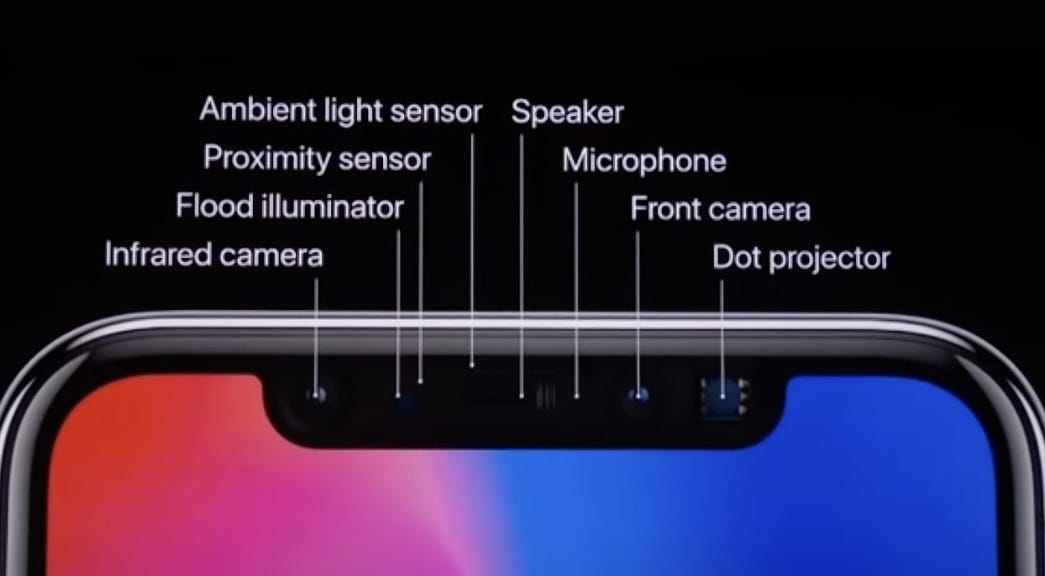
are expected to be the largest future adopters of metalens-based optical systems.
Metalenses are no longer a laboratory curiosity—they have entered the OEM/ODM supply chain as a viable option for next-generation thin, planar optics. As 3D sensing, computational photography, AR devices, and optical interconnects continue to expand, the metalens ecosystem is transitioning rapidly from research to commercial deployment.
Four Major Challenges for Metalenses
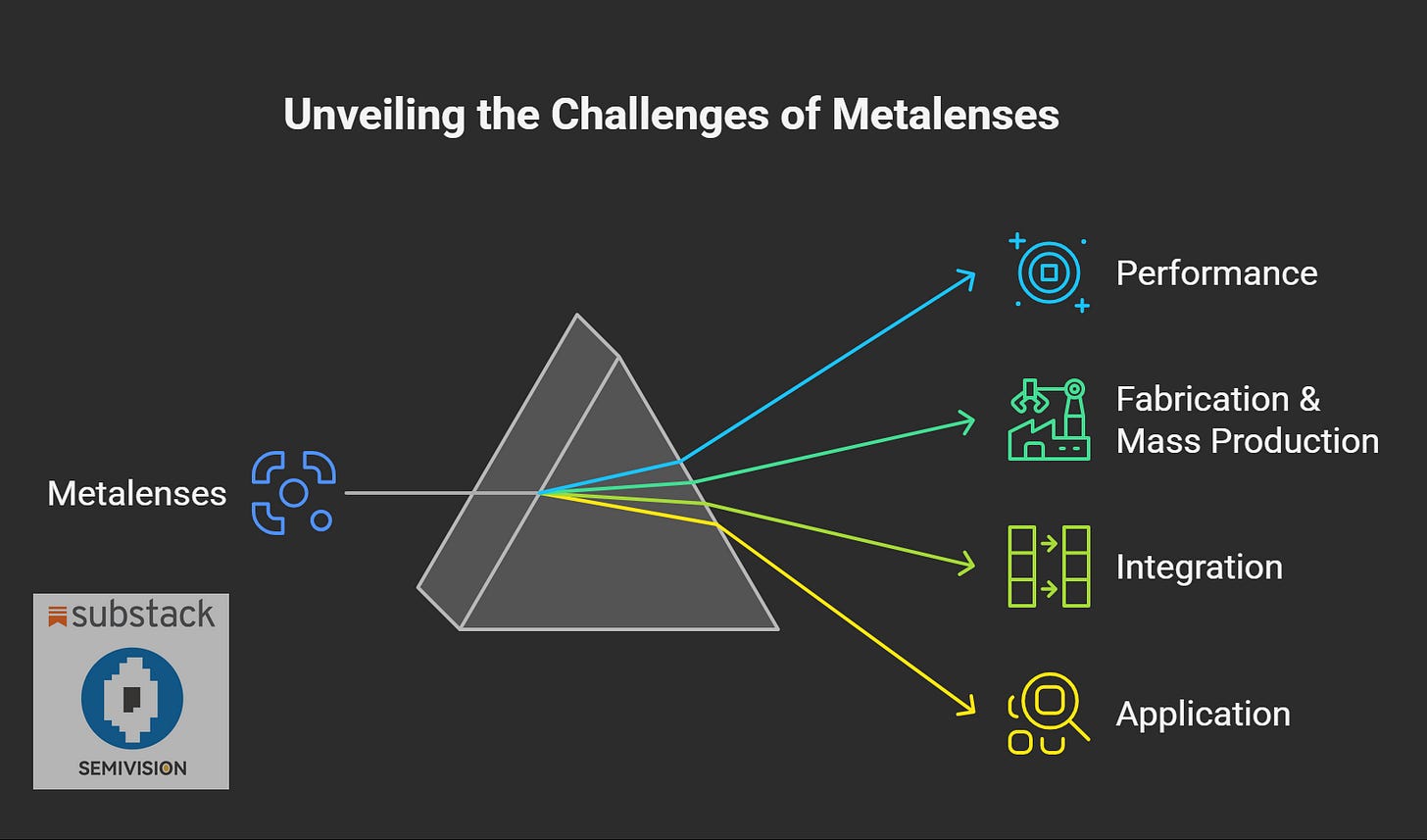
Finally, we discuss the key obstacles facing metalenses.SemiVisionclassifies them into four categories:
- Performance
A practical metalens must achievebroadband operation, low chromatic aberration, and high optical efficiency(including transmission, f-number, and NA). In real optical modules, however, additional challenges arise:
wide distribution of incident angles
varying polarization states
temperature- and wavelength-dependent drift
sensitivity to manufacturing tolerances
Meeting all of these simultaneously remains one of the most demanding aspects of metalens design.
- Fabrication & Mass Production
Current mass-production routes include:
DUV / EUV projection lithography— suitable for large-area, all-glass metalenses
Nano-imprint / UV-imprint lithography— suitable for low-cost, high-volume replication on plastic or glass substrates
Each route must balancecost, resolution, and throughput, while also managing mold lifetime, defect density, and alignment errors. Achieving semiconductor-grade yields for sub-wavelength nanostructures is still a major industrial challenge.
- Integration
Metalenses are often attached directly onto CIS sensors, VCSELs, fiber arrays, or waveguides. These systems impose extremely tight packaging tolerances and significant thermo-mechanical stress.
High-NA and short-focal-length designs are particularly sensitive—small positional errors can cause substantial performance degradation, posing a major barrier to mass-production yield and reliability.
- Applications & Business Models
The most mature applications today include:
Face ID / 3D sensing
CIS optical enhancement
optical couplers for communication
AR/VR optics
compact or compressed cameras
Replacing a full smartphone camera lens stack will require more time and further co-optimization of optics, sensor design, and computational algorithms.
However, metalenses are already being adopted in several niche markets, such as ultra-thin cameras, on-chip microscopes, and packaging-level optics for photonics.
When and where did Meta-Optics technology originate?
Meta-optics as a field can be traced back clearly to theearly 2010s, when researchers began using nanoscale structures to redefine phase control in optics—pushing optical design from curved refraction into the era of engineered nanostructures.
- Conceptual Origin (2011): Phase Discontinuities and the Birth of Meta-Optics
The foundation of meta-optics was established in 2011, when Prof. Federico Capasso’s group at Harvard University published a landmark paper inScience.
This work demonstrated that arrays of nanopillars could manipulate the phase of light at will, introducing:
phase discontinuities, and
the generalized laws of reflection and refraction.
The nanostructures used were on the order of 50–200 nm, three orders of magnitude smaller than conventional micron-scale optical components.
Capasso’s early demonstrations operated primarily in the mid-infrared spectrum (8–10 µm), showing that carefully designed nanoantenna arrays could arbitrarily shape outgoing wavefronts.
This laid the mathematical and physical foundation of metasurface optics.
- Emergence of Imaging Applications (2016): Metalenses Enter the Visible Domain
Roughly five to six years after the first demonstrations, researchers achieved a major breakthrough: the transition from infrared to visible-light metasurfaces.
By 2016, the Harvard team succeeded in demonstrating visible-light flat lenses, proving that nanostructures on a single thin film could replicate the focusing power of traditional refractive lenses—and even replace multi-element lens stacks.
This marked the point at which meta-optics moved beyond academic theory and the metalens as a practical optical component was born.
- Beginning of Commercialization: Founding of Metalenz
Following the 2016 breakthroughs, the technology progressed toward real-world deployment.
Prof. Capasso and his graduate students founded Metalenz (originally named Meta Lens), aiming to bring meta-optics from laboratories into commercial products.
Metalenz’s founding symbolized the transition of meta-optics from research to manufacturing, and initiated a new engineering chapter involving:
CMOS-compatible fabrication
glass-substrate processing
wafer-level nanostructure mass production
This marked the official starting point of meta-optics commercialization.
How did Meta-Optics move from lab research to real mass production and broad adoption?
The journey of meta-optics from laboratory research to mass production and mainstream applications is essentially a story of“from nanostructure to market.”It has been driven by deep academic breakthroughs, steady maturation of manufacturing technologies, and the pull of major customers adopting the technology at scale.
The starting point lies in the light-field control enabled by nanostructures. Instead of the traditional micron-scale optics, meta-optics operates at the 10⁻⁹ m scale, using structures such as nanopillar arrays with feature sizes on the order of 50–200 nm. In 2011, a team at Harvard University first demonstrated, in the long-wavelength spectrum, that specially designed nanopillars could manipulate the phase of light, laying the theoretical foundation of meta-optics. By 2016, they showed that these structures could form a focusing element in the visible spectrum, marking the true birth of flat optics. During this period, the Harvard group spun out Metalenz, one of the first companies in the world explicitly founded to bring meta-optics from the lab into real markets.
From that point on, the main challenge for meta-optics was no longer the optical model, but “how to manufacture it at scale.” Moving from research prototypes to wafer-level manufacturing means every single nanopillar must be replicated with extremely high uniformity across a large substrate—an enormous challenge for process engineering.
Manufacturing of meta-optics relies heavily on semiconductor technologies. Today, deep-UV (DUV) lithography combined with dry etching remains the mainstream high-precision approach, particularly for high-end all-glass or dielectric metalenses. Nanoimprint lithography (NIL), on the other hand, offers a pathway toward lower cost and large-area replication, enabling high-resolution patterns in both organic and inorganic materials. The period from roughly 2016 to 2022 is often seen as an industrial “gap,” not because nothing happened, but because many companies were quietly exploring how to scale nanostructures to full wafers and build a reliable, repeatable manufacturing chain.
As manufacturing capabilities gradually matured, meta-optics began its true commercialization phase. In 2022, Metalenz and STMicroelectronics announced the first mass-produced meta-optics product, signaling that meta-optics had entered industrial-grade applications. Metalenz also announced collaboration with UMC to fabricate Polarization ID (PID) architectures at the wafer level, with the goal of mass production. These foundry partnerships marked a transition from small demo runs and academic prototypes to high-reliability commercial platforms.
Adoption by major customers has been a key accelerant. Apple had already introduced components with metasurface structures into the Face ID module of previous-generation iPad Pro, demonstrating maturity in 3D sensing and projection optics. Although large-scale adoption in iPhone camera stacks has not yet materialized, Apple, Google, and Samsung are all reported to be evaluating or testing such elements. Their eventual decisions will be critical in determining when meta-optics truly “goes mainstream.”
Today, meta-optics has already proven its value in multiple fields:
Face ID and 3D sensingare the most mature mass-production applications. Meta-optical elements can integrate multiple optical functions into a single component, allowing traditional multi-element lens stacks to be compressed into one metasurface.
Polarization ID (PID)is an emerging application that uses differences in polarized reflections from skin and sub-surface scattering to distinguish live tissue from spoofed inputs. This can provide more secure and simpler identity verification with a single flood illuminator plus a polarization-selective metalens.
InCMOS image sensors (CIS), nanostructures integrated on the sensor surface can significantly improve the efficiency of blue and green light (by roughly40% and 16%, respectively), especially for very small pixels around0.8 µm, where conventional microlenses are reaching their limits.
Meta-optics is also viewed as a key enabling technology forAR/VR, as it can greatly reduce the weight and volume of optical modules while integrating multiple functions. Future roles includecollimators,waveguide couplers, and ultra-compact cameras.
Looking ahead tooptical communications and CPO (Co-packaged Optics), as fiber arrays move to higher densities (e.g., 2D fiber arrays), meta-optics offers strong advantages in beam shaping and coupling efficiency. Its multi-channel wavefront control capabilities naturally suit high-density fiber-coupling modules.
However, despite its large potential, meta-optics still faces significant barriers before it can fully replace traditional lenses. The biggest technical challenge isachromatic performance.
Traditional achromatic lenses often rely on5–7 lens elementsmade of different materials and curvatures to correct dispersion across multiple wavelengths. By contrast, achieving the same effect with asingle metasurfaceover a broad spectrum is extremely hard, because it simultaneously stresses:
material dispersion engineering,
nanostructure design, and
process control.
Although lab-grade full-color metalens imaging has already been demonstrated, commercial products remain limited. Another challenge arises from the extreme sensitivity of nanostructures: process variations, sidewall roughness, structural collapse, and metrology difficulties can all degrade efficiency and yield.
In summary, the industrialization of meta-optics is like a journey from handcraft to an industrial revolution. Ten years ago, it was a niche nano-optics experiment in university labs; today, it can be produced at wafer scale and has already been deployed in 3D sensing, polarization recognition, and CIS. The next stage of challenges will center on more demanding markets such as broadband imaging, AR optics, and high-density optical communications. With ongoing advances in materials, processes, and optical algorithms, meta-optics has a real chance to reshape the optical architectures of cameras, sensors, and optical interconnects over the next decade.
What challenges and opportunities does Meta-Optics face today, especially in AR and imaging?
Meta-optics (including metalenses and metasurfaces) is triggering a structural transformation in optics. In less than a decade, it has moved from laboratory exploration to industrial manufacturing and real-world deployment, becoming a classic case of “huge opportunity × high technical difficulty” in AR and imaging.
Its core value lies in this: functions that once required multiple refractive lenses, diffractive optical elements (DOEs), and filters can now be compressed into a single, ultra-thin planar component. This makes multifunctional flat optics real, not just as a concept, but as an engineering solution—particularly strategic for any system that needs to be smaller and more capable, such as 3D sensing, CIS, and AR devices.
Inimaging and 3D sensing, meta-optics has already moved from “concept” to “deployment.”
In consumer electronics, teardown analyses of Apple’s iPad Pro Face ID / 3D structured-light module have confirmed the presence of metasurface-based optical elements. This shows that the technology is no longer confined to papers and demos—it is embedded in actual product generations.
Traditionally, Face ID consists of multiple optical modules: Dot Projector, Flood Illuminator, and IR Camera, each with its own lens and DOE. The long-term goal of meta-optics is to gradually collapse these functions into a single optical element, making the module thinner, simpler, and easier to assemble and mass-produce, without compromising precision or security.
A natural extension of this idea is PID (Polarization ID): using a planar metalens together with polarization imaging to analyze differences between surface reflection and subsurface scattering of skin, thus providing identity verification and liveness detection. Architecturally, this could reduce the system to a broad illuminator plus a single polarization-selective meta-optical element, potentially replacing more complex Face ID optics.
ForCIS, meta-optics is used forpixel-level light-field engineering:
At pixel sizes around0.8 µm, nanostructures can replace traditional microlenses, re-routing blue and green light more efficiently into the photodiodes.
Reported results show around40% improvement in blue-light efficiencyand~16% for green, expanding the performance envelope of high-end sensors in a regime where aperture and pixel area are severely constrained.
Some companies have also built ultra-small camera modules using just two metalenses plus a sensor, proving feasibility for extreme miniaturized imaging and even winning international design/innovation awards.
Looking ahead to automotive and robotic vision, as demand grows for 3D sensing, short-range ToF, polarization imaging, and IR vision, meta-optics is well positioned for multi-modal sensing and compact optical-mechanical modules.
In theAR/VRspace, meta-optics is considered a key accelerator of next-generation optical architectures:
Metalenses are typically only 0.5–2 µm thick, adding almost no weight, which is crucial for AR glasses requiring long wear times and tight weight budgets.
Most current AR engines still depend on birdbath optics or waveguide architectures, which involve multiple curved lenses, prisms, and in/out-coupling gratings.
One major direction in meta-optics development is to integrate these functions into just a few flat optical elements—for example, embedding metasurface structures directly into glass, so that real-world scenes and projected images enter the eye through different angles or polarization channels. The industry’s expectation can be summarized as “simplify light paths, reduce optical components.”
But for meta-optics to truly enter mainstream imaging markets (e.g., smartphone main cameras or full-color AR displays), two fundamental issues remain extremely challenging.
First: Full-color imaging and chromatic aberration.
Achieving broadband achromatic performance is considered the “Holy Grail” of meta-optics. Conventional lens stacks leverage 5–7 lens elements with different materials and curvatures to correct focus shifts across red, green, and blue bands. For a single metalens, achieving high efficiency and nearly constant focal length across 400–700 nm or even wider bands pushes:
nanostructure design,
material dispersion engineering, and
process precision
to their limits. Consequently, most mass-produced meta-optics today targetsingle-wavelength or narrowband applications—for example, 940 nm IR for Face ID, or specific bands for industrial and medical imaging. High-quality RGB full-color AR displays would require high efficiency, low dispersion, and high uniformity across the full visible band, which remains largely confined to laboratory demonstrations and prototypes, far from the robustness and yield expectations of smartphone main cameras.
Second: Process and mass production.
Meta-optics unit cells typically fall in the50–200 nmrange, often requiring:
high aspect ratios,
smooth sidewalls, and
precise height control
to maintain phase and efficiency. At the wafer level, this essentially forces the use of semiconductor manufacturing: DUV lithography plus dry etching, or NIL-based master molds with high-volume replication. Mainstream high-reliability products generally rely on inorganic materials (glass, silicon, TiO₂, SiNₓ, etc.) to ensure long-term stability and environmental robustness. Plastics can be patterned via NIL for low-cost structures, but limitations in heat resistance, moisture stability, and long-term dimensional stability tend to confine these to mid–low-end or short-lifetime applications.
Even when the process technology is in place, manufacturers must still simultaneously optimize:
optical efficiency,
image quality,
structural yield, and
AOI inspection and metrology.
This is a continuous engineering challenge for both foundries and optics suppliers.
In driving the industrialization of meta-optics, major tech companies and specialized meta-optics vendors have played critical roles:
Appleis one of the earliest brands to introduce meta-optical structures into commercial products. In the iPad Pro Face ID module, metasurface traces can already be identified. Through patents (e.g., MOE-based illumination concepts), Apple is actively exploring how a single meta-optical element can handle projection, beam shaping, and illumination simultaneously. Strategically, Apple aims to use meta-optics to gradually replace multiple refractive lenses and DOEs in 3D sensing modules, making them thinner, simpler, and easier to package.
Metalenz, spun out of Harvard, is one of the key technology enablers of meta-optics commercialization. The company claims to have shipped hundreds of millions of meta-optical components into various modules. Together with STMicroelectronics, it launched the first mass-produced meta-optics-based product, and with UMC, it is preparing to bring PID into volume production—signaling the emergence of a “meta-optics foundry ecosystem” where wafer fabs and optics IP houses collaborate closely.
Companies likeNILT, with deep expertise in nanoimprint lithography, have demonstrated ultra-compact cameras composed of just two metalenses plus a sensor, winning international awards. Their strategic value has led to acquisition by larger groups, solidifying their role in the flat-optics supply chain.
In the CIS domain, major sensor makers such as Sony have begun incorporating meta-optics concepts into pixel-level designs to improve short-wavelength efficiency and angular tolerance. System and device companies like Google and Samsung are testing metasurface components in 3D sensing, ToF, and AR to evaluate advantages in module thickness, power consumption, and design freedom.
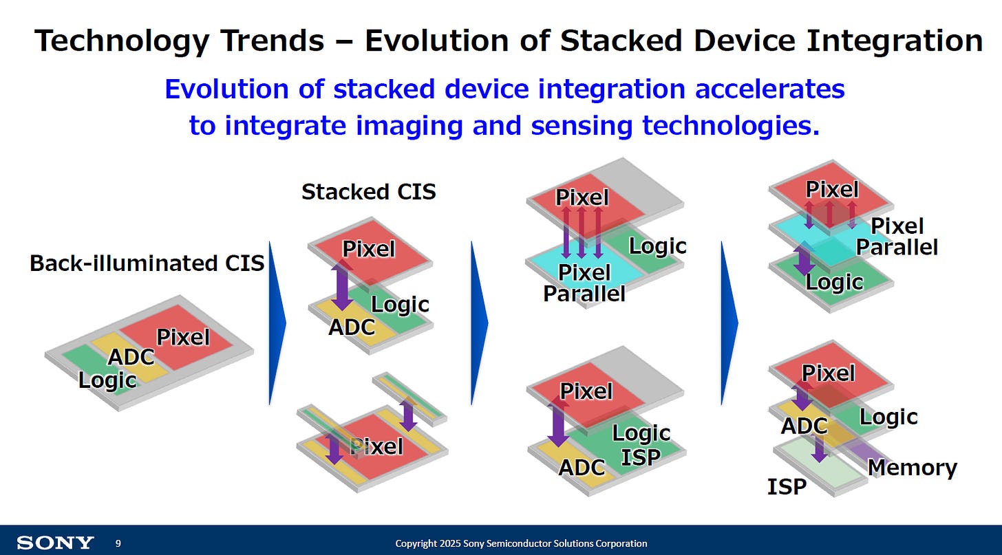
Overall, the shared motivation across these tech companies is clear: leverage the light-field control freedom offered by nanostructures to achieve smaller, thinner, more multifunctional, and more planar optical modules that meet next-generation requirements in Face ID, 3D sensing, CIS, and AR/VR.
Taking a step back, meta-optics has already established itself as a “mass-producible, integrable solution” in niche but high-value markets such as 3D sensing, polarization ID, CIS optical enhancement, and micro-optical systems. Whether it will, can, and when it might truly replace traditional multi-element lenses—for full-color main cameras or as the core display optics of AR glasses—ultimately depends on two questions:
Can broadband achromatic design and fabrication be fully solved?
Can wafer-level nanostructure manufacturing achieve the required efficiency, yield, and reliability?
If we liken meta-optics to askyscraper in the world of optics, then:
we have already built a solid foundation in nanostructure design, monochromatic imaging, and 3D sensing,
But to reach the top—to fully capture full-color, high-resolution cameras and AR glasses as core optical engines—we still need breakthroughs in the three “steel columns” of materials, structures, and processes that can finally overcome dispersion and manufacturing limits.


PreviousNext
TopLatestDiscussions








See all