TSMC COUPE × Metalens: Building the Key Optical Architecture for NVIDIA’s Next-Generation AI Interconnect
TSMC COUPE × Metalens: Building the Key Optical Architecture for NVIDIA’s Next-Generation AI Interconnect
- Source: SemiVision
- Author: SEMIVISION
- Published: 2025-11-29T07:58:32+08:00
- URL: https://tspasemiconductor.substack.com/p/tsmc-coupe-metalens-building-the TSMC COUPE × Metalens: Building the Key Optical Architecture for NVIDIA’s Next-Generation AI Interconnect


TSMC COUPE × Metalens: Building the Key Optical Architecture for NVIDIA’s Next-Generation AI Interconnect
Original Article By SemiVision Research (TSMC,UMC,Nvidia ,Marvell ,Broadcom,HiMax ,VisEra,AuthenX ,Ayar Labs, Brillink.ai,Latitude Design Systems,Foxconn,Marvell ,Broadcom )

Nov 29, 2025
∙ Paid

The 2025 SWTest conference delivered a very clear message to the industry: testing is no longer a supporting role in manufacturing—it has become the central technological hub for advanced packaging, AI/HPC, and optoelectronic integration. As AI GPUs and dedicated accelerators push power consumption to new extremes, chiplets move toward large-scale commercialization, N2/A16 nodes adopt BSPDN, HBM stacks grow deeper, and CPO/OIO enters the early stages of production planning, the entire industry now recognizes a simple truth: without testing, none of the innovations in front-end process or advanced packaging can be realized.
This year, whether from keynote talks by Micron, Marvell, Advantest, Teradyne, MPI and other leading companies, or from technical discussions throughout the forum, one theme was consistent:testing is now essential for high-speed SerDes, KGD validation, multi-stacked memory, system-level reliability, and thermal integrity.As AI/HPC chips increase in package size and push signaling frequency ever higher, test strategies must evolve beyond traditional wafer sort toward a newelectrical × optical × thermaltri-domain framework. This shift is gradually turning testing into a critical engineering platform—one that will shape the next decade of semiconductor processes and advanced packaging architectures.
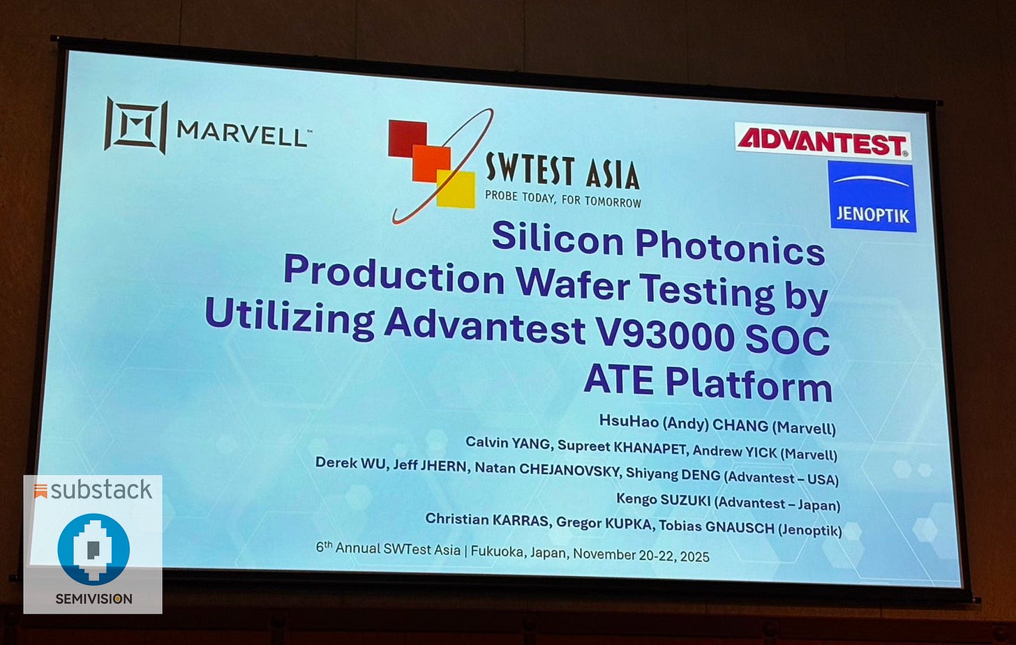
On the other hand, one of the most compelling revelations at this year’s SWTest was the fact thatsilicon photonics (SiPh), CPO (Co-Packaged Optics), and Optical I/O testing topics finally moved to center stage. From wafer-level photonic test and optical-alignment platforms, to 2D/3D FAU (Fiber Array Unit) coupling accuracy, DWDM multi-wavelength characterization, and BER/eye-performance evaluation for 800G and 1.6T optical engines, the entire photonic-test ecosystem is rapidly converging toward mass-production maturity.
CPO and OIO are among the most critical technologies in today’s AI data-center roadmaps. The deep discussions this year—covering fiber-array tolerances, coupling margins, packaging repeatability, and thermal-variation behavior—clearly show that the industry is now confronting the real barrier ofopto-electronic heterogeneous-integration testing. Even more importantly, probers and probe cards are no longer merely electrical interfaces; they are evolving intomulti-modal test platformsthat simultaneously support electrical probing, optical coupling, and thermal conditioning.
Overall, SWTest 2025 did more than showcase new technologies—it revealed a profound structural shift:testing is redefining the logic of advanced packaging and optoelectronic integration, and over the next 3–5 years, testing will become an unavoidable core battleground for the entire AI semiconductor industry.
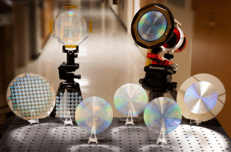
In today’s focus, we turn toMetalens, a breakthrough technology that has rapidly drawn intense attention across the semiconductor and photonics sectors. Since TSMC demonstrated the use of Metalens as an optical-coupling element in itsCOUPE (Compact Universal Photonic Engine)platform, many readers have begun asking:
• What exactly is the role of Metalens?
• How is it fundamentally different from traditional µLens or micro-lens arrays?
• Why is it emerging as a key interface for silicon photonics (SiPh) in chip-to-fiber and chip-to-chip optical links?
This article aims to answer these questions from a technical perspective. We will break down Metalens working principles, fabrication characteristics, and wavefront-engineering methods, and examine how Metalens can integrate with silicon-photonics platforms—covering grating couplers, edge couplers, meta-surface mode transformers, and more. We will also map out its potential integration pathways in future CPO/OIO architectures.
In other words, after reading this, you should not only understand what a Metalens is—you should clearly seehow it opens new engineering design space for next-generation optical packaging and PIC-coupling interfaces.

Driven by the demand for higher bandwidth and lower power consumption in high-performance computing, AI, and data center applications, silicon photonics is rapidly emerging as a key technology for next-generation data transmission and advanced packaging.
The Compact Universal Photonic Engine (COUPE) platform jointly developed by TSMC and NVIDIA is reshaping the landscape of optoelectronic integration. COUPE not only integrates an advanced Co-Packaged Optics (CPO) architecture but also establishes a scalable, production-ready photonic integration framework across optical coupling, packaging, and materials engineering.
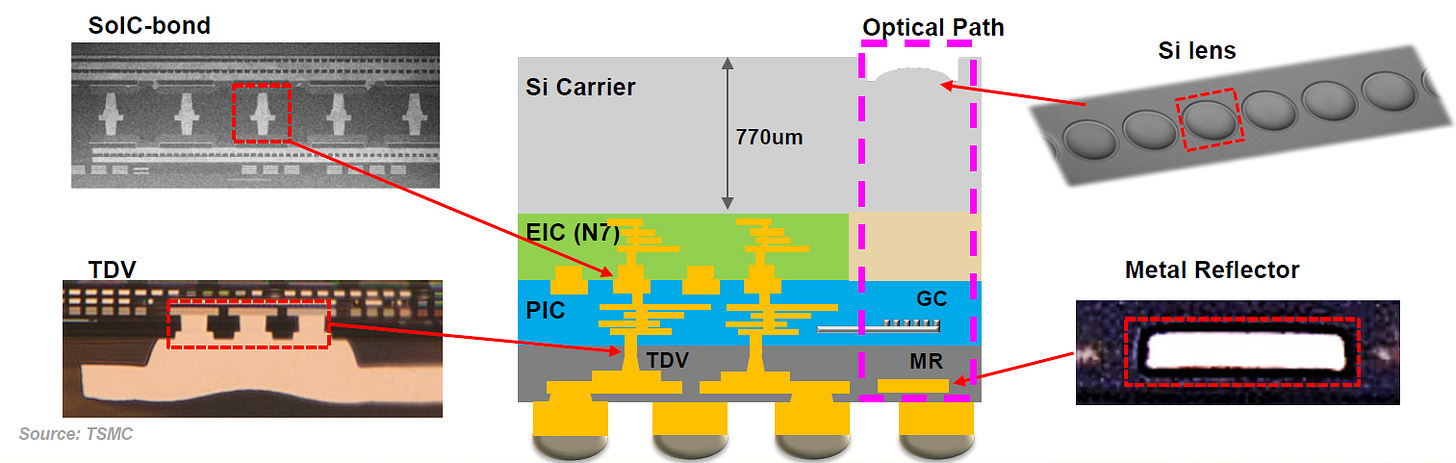
Within this ecosystem, the Meta Lens plays an irreplaceable role in optical I/O evolution. Traditional optical couplers rely on 1D Fiber Array Units (FAU), but the growing need for multi-channel, multi-wavelength, and high-density interconnects is driving a transition toward 2D FAU structures. The Meta Lens, with its ultrathin and programmable wavefront control capability, perfectly supports this geometric transition—enhancing fiber-coupling efficiency and beam-shaping performance.
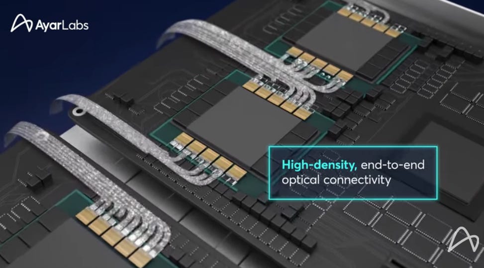
Companies such asAyar Labshave demonstrated the practicality of integrating Meta Lenses as beam directors and mode-field modulators in optical I/O modules. More importantly, the introduction of emerging materials such asTFLN(Thin-Film Lithium Niobate),BTO(Barium Titanate), and optical polymers provides Meta Lenses with the potential for nonlinear optical effects and hybrid material integration. When these are co-integrated with photonic integrated circuits (PICs) on silicon platforms, Meta Lenses evolve beyond passive focusing—they become active, tunable optical elements capable of adjusting wavelength, polarization, phase, and even performing dynamic control.
Over the past two years, Ayar Labs has clearly accelerated its deployment in the Optical Engine domain, especially as the industry increasingly converges on the positioning of Optical I/O (OIO). According to the latest industry information and public announcements, Ayar Labs has not only entered a deep collaboration with Taiwan’s GUC (Global Unichip Corp.), combining its TeraPHY™ optical-I/O chiplet with GUC’s advanced ASIC design and packaging-integration capabilities, but is also working closely with multiple design teams at AIChip (Alchip Technologies). The goal is to co-develop next-generation optical-electrical interconnect architectures tailored for AI/HPC workloads.
This signals thatAyar Labs now formally regards Taiwan as one of its most critical ecosystems for Optical–Electrical Heterogeneous Integration—not just as a technical partner, but as a true high-volume manufacturing (HVM) supply-chain hub capable of delivering production-scale optical engines.
At the same time, within the broaderOptical Interconnectionlandscape, Ayar Labs’ strategic direction is becoming increasingly differentiated from several rapidly rising photonic-interconnect companies. Celestial AI is pushing its Photonic Fabric; Lightmatter is driving Passage; Lightelligence is focused on photonic-accelerator architectures; and Ranovus is known for low-latency optical links. Each company emphasizes a different “photonics-to-compute” paradigm.
Ayar Labs, however, has a distinctly clear strategy:
It focuses on silicon-photonics-based Optical I/O embedded directly inside the package, aiming to replace high-power, EMI-prone, and scaling-limited high-speed SerDes and become the critical communication pathway inside future AI clusters. Put differently:
Celestial AI and Lightmatter are redefininghow GPUs communicate with each other.
Ayar Labs is redefininghow a chip inputs and outputs data in the first place.
Viewed from a system-level perspective, Ayar Labs now occupies a strategically significant position. Its technology direction aligns directly with a key industry reality: as AI model scales explode,the package boundary has become the new bottleneck. And its intensive collaboration with the Taiwanese ecosystem gives Ayar Labs a credible path towardtrue HVM readiness.
This is why many recent industry analyses now view Ayar Labs asone of the most important companies to watchas optical engines and optical interconnect rapidly move toward becoming mainstream components of future AI infrastructure.
TSMC’s deepening collaboration with NVIDIA further reinforces the strategic importance of the COUPE platform.
As the COUPE platform advances, it is evident that Meta Lenses hold strategic value in multiple domains—optical packaging, FAU evolution, beam coupling, material integration, and power control. The collaboration between TSMC and NVIDIA underscores a broader paradigm shift: packaging is no longer a purely mechanical process but a multi-dimensional integration of optics, electronics, thermals, materials, and algorithms.
2025年6月2日
2025年6月25日
The customizable structural design of Meta Lenses, coupled with their integration into EDA design environments, introduces new challenges for optical parameter synthesis and automated layout generation within the semiconductor design ecosystem. Consequently, from material selection and design workflows to wafer-level fabrication, bonding, packaging, and system integration, Meta Lenses are no longer optional accessories—they are emerging as core modules in next-generation optical packaging.
The industrial value chain surrounding Meta Lenses is expanding rapidly, encompassing mold fabrication, laser direct writing, AI-assisted design synthesis, meta-optical material deposition, and mass-production module packaging. If Taiwan can establish leadership in fabrication process development, EDA integration, and module validation, it will secure a vital position in the global competition for advanced optical platforms.
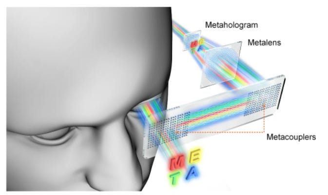
Optical components play a pivotal role in modern electronic and optoelectronic systems. However, conventional lenses are typically bulky and heavy, posing significant limitations on the miniaturization of optical systems. Meta-lenses, a class of flat optical devices based onmetasurfaces, offer a transformative solution by manipulating the phase of incident light at the nanoscale using engineered subwavelength structures on a planar substrate. These ultra-thin, lightweight, and CMOS-compatible optical elements can replicate — and in some cases surpass — the functionalities of traditional curved lenses.
Unlike conventional microlens arrays that rely on geometric curvature for light focusing, meta-lenses enable arbitrary wavefront shaping through spatially varying nanoantenna patterns. This breakthrough opens up novel possibilities for integration into chip-scale systems such as image sensors, AR/VR displays, LiDAR modules, and silicon photonics platforms.
This report provides a comprehensive analysis of meta-lens technology, covering its physical principles and design architectures, performance comparison with traditional microlenses, integration with silicon photonics, fabrication processes and associated challenges, current real-world applications, ongoing research directions, and the key technical hurdles that must be overcome to unlock its full commercial potential.
With the growing demand for optoelectronic integration, we are witnessing for the first time on TSMC’s COUPE platform the use of metalens as a core element for optical coupling—signaling that metasurface technology has officially entered the engineering mainstream of chip packaging and optical interconnects.
A metalens is not merely a new type of lens; it is an ultrathin optical interface that can be fabricated directly on a wafer and bonded with optoelectronic components, making it a fundamental building block for CPO, silicon photonics, AR/VR sensing, and 3D light-field systems.
On the COUPE platform, wafer-level optical coupling schemes utilizing metalens structures have already emerged. These leverage subwavelength metasurfaces to achieve high-efficiency, low-tolerance vertical coupling between light-emitting arrays and silicon photonic chips—heralding a future where CPO and Optical I/O systems are defined by ultrathin, wafer-scale, and mass-producible optical designs.
To understand the technology and industry dynamics driving this trend, we will first explore the physical principles and evolution of metalens technology, and then move to its industrial implementation—examining howHon Hai Research Institute (HHRI)systematically advances metasurface modularization and mass production, while UMC and Metalenz jointly build a large-scale metasurface fabrication line on a 40 nm CMOS platform. Together, these dual axes of system integration and manufacturing illustrate Taiwan’s pivotal role in the emerging metalens/metasurface ecosystem.
ProfessorHao-Chung Kuoand ProfessorYao-Wei Huang’s team is featured on the cover story of Nano Letters!
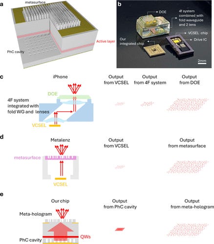
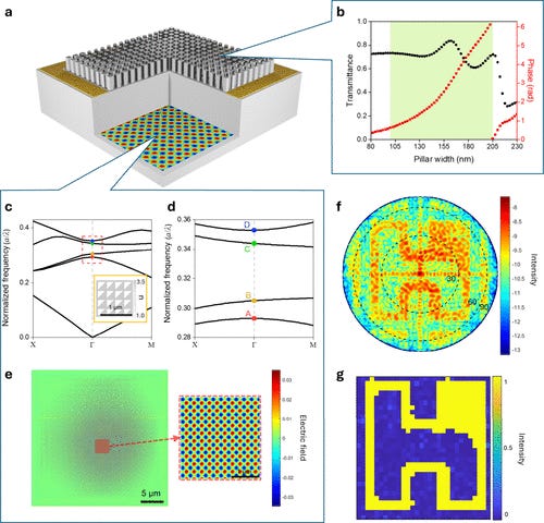
The team has successfully developed a monolithically integrated metasurface–PCSEL chip for depth sensing, achieving for the first time the on-chip integration of a metasurface hologram and a photonic crystal surface-emitting laser (PCSEL) to realize a chip-scale structured light projector.
This breakthrough work is published in the world-leading journal Nano Letters and has been selected as the July issue cover and cover story, opening up new possibilities for next-generation biometric identification, extended reality (XR), and consumer electronics depth-sensing technologies.
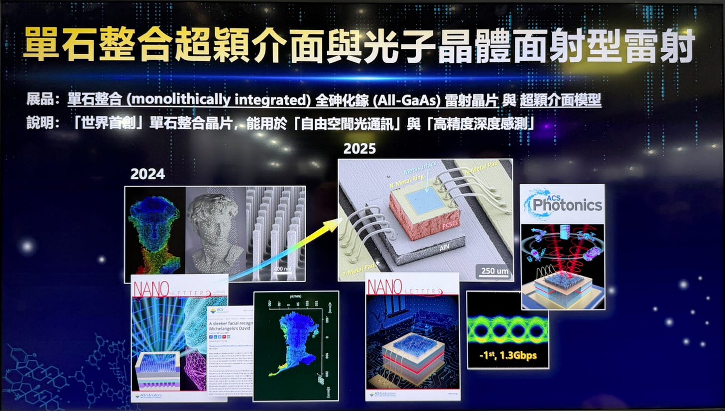
Reference: https://pubs.acs.org/doi/10.1021/acs.nanolett.3c05002
2025年5月4日
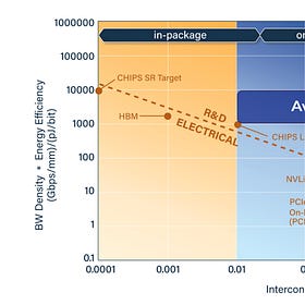
At this year’s #OFC25 conference and in recent discussions on optical interconnect technologies, optimizing the power efficiency, bandwidth, and transmission range of short-reach interconnects within data centers has become a core topic, driving the emergence of several innovative architectures. Among these, microLED-based optical interconnects have drawn significant attention. MicroLEDs are micron-scale gallium nitride (GaN) light-emitting diodes capable of efficiently emitting photons under electrical current. Unlike traditional VCSELs or external laser sources, microLEDs act as self-emissive microscale light sources, offering a simplified structure, low energy consumption, and full compatibility with CMOS manufacturing platforms—making them ideal for building high-channel-count, massively parallel optical interconnect systems.
2025年4月14日

The Foxconn Research Institute has provided strategic insights into the silicon photonics industry, underscoring its critical role in meeting the rising demands of high-performance computing (HPC) and artificial intelligence (AI) applications. The institute identifies silicon photonics as a foundational technology for overcoming bandwidth bottlenecks and enhancing energy efficiency within modern data centers. To advance its competitiveness in optical communication and interconnect solutions,
Before delving into the technical foundations of metalenses, it is also crucial to recognize another major shift: Taiwan is no longer merely a base for metal wiring, packaging, and CMOS fabrication, but is becoming a core global hub for transforming metasurface research into commercial products. The most representative example of this transformation is the comprehensive technology roadmap established by HHRI in recent years.
Unlike many research groups still focused on isolated device design, HHRI’s strategy emphasizes system-level integration—spanning metasurface design, wavefront control, active light-source integration, modular packaging, and automated metrology. Through this vertically integrated approach, HHRI has built a metasurface technology stack capable of supporting mass production, marking the first time Taiwan possesses true product-grade metasurface capabilities and forming a complementary linkage with TSMC and UMC on the wafer fabrication side.
In addition to this, the Hon Hai Research Institute recently published a new paper, focusing primarily on the topic of…


It is precisely these synergistic interactions between industry and research that allow us to examine the following topics from a higher vantage point:
Evolution of Metalens Technology and HHRI’s Systematic Development
Since Snellius formulated the law of refraction in 1621, optical design has been fundamentally based on curved-surface lenses. Traditional glass or plastic lenses rely on controlling curvature and optical path differences to focus light — forming the foundation for over four centuries of imaging, photography, and sensing applications.
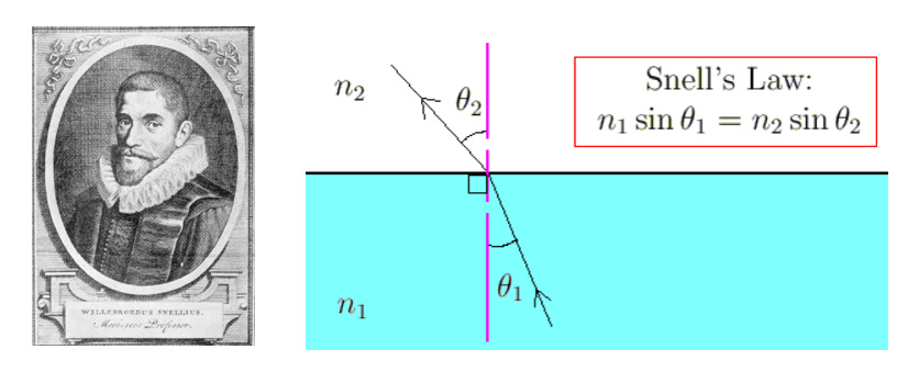
However, as devices become thinner, chip-scale packaging (CSP) rises, and AI and high-speed optoelectronic systems grow rapidly, these conventional bulky lenses have revealed inherent limitations in volume, weight, and integration.
Entering the 21st century, the maturity of nanofabrication and metamaterial engineering has triggered a fundamental revolution in lens technology. Early 3D metamaterials demonstrated exotic phenomena such as negative refraction and cloaking, but the real turning point came in 2011, when Federico Capasso’s team at Harvard introduced the concept of the metasurface.
This marked a paradigm shift in optical engineering—from 3D refractive structures to 2D subwavelength arrays capable of precisely manipulating phase, amplitude, and polarization.
The metalens, a direct derivative of this concept, achieves optical focusing and wavefront control comparable or even superior to traditional lenses, within only a few hundred nanometers of thickness.
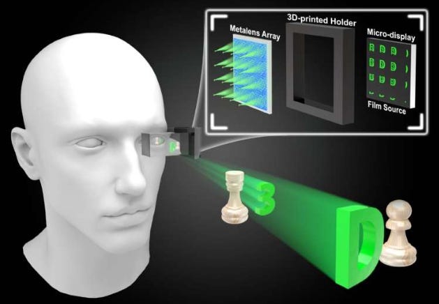
Such characteristics—ultrathin form factor, wafer-level manufacturability, and direct bondability to sensors and photonic chips—make the metalens a foundational enabler of modern optoelectronic integration. Consequently, it has become a core component in Co-Packaged Optics (CPO), optical interconnects, AR/VR, and 3D sensing systems.
2025年9月4日
In this global wave, theFoxconn Hon Hai Research Institute (HHRI)is taking a markedly different path from academia: instead of remaining at the level of isolated optical designs, it is driving metasurface commercialization through a fully system-level approach. HHRI’s Semiconductor Research Center has designated metasurfaces as an official core research direction, committing long-term resources under a “academia → module → mass production” strategy. ItsMeta-PCSELproject withNYCUstands as the best example: by integrating a metasurface directly onto the PCSEL surface, the team reduced the module volume for depth sensing and spatial light-field computation to just 0.025 mm³, lowered power consumption by nearly 30%, and broke through long-standing miniaturization limits of light-field modules. The work not only demonstrates HHRI’s capability in metasurface design, but also establishes its technical depth in active-light-source–integrated metasurface systems. HHRI is simultaneously building results in polarization beam-splitting, wavefront control, and other domains, indicating that its roadmap has already moved beyond passive components into active-source architectures.
HonHai’s greatest advantage is not a single optical breakthrough, but its vast manufacturing and packaging infrastructure, which enables metasurfaces to be inserted directly into mass-production-ready processes. From WLP and CSP to heterogeneous integration, optical module bonding, passive alignment, and automated testing, Foxconn possesses the full production chain required to meet metasurface demands for large-area uniformity, bonding precision, and module-level packaging. This makes HHRI one of the very few teams globally capable of taking optical design all the way to product-grade module integration—particularly suited for AR/VR light-field engines, 3D sensing, LiDAR, and the emerging generations of optical I/O and CPO interconnects. Metalenses can be applied directly to beam engineering at the FAU, VCSEL, and PD interfaces in these systems, offering high degrees of design freedom and extremely compact form factors. Overall, HHRI’s direction has already moved beyond the boundaries of traditional research institutions, gradually establishing a “mass-producible metasurface module platform”—a strategic position that will shape Taiwan’s role in the next era of optical semiconductors.
UMC × Metalenz: The Strategic Logic Behind Building the World’s First Large-Scale Metasurface Production Line on a 40 nm CMOS Platform
Unlike HHRI’s system-level approach, UMC (United Microelectronics Corporation) is pioneering a globally rare, forward-looking strategy from the wafer-level manufacturing side. In 2025, Metalenz announced that it would adopt UMC’s 40 nm CMOS platform to fabricate its meta-optics layer and perform wafer-on-wafer (W2W) bonding with image sensors using a 300 mm production line. This collaboration positions Taiwan as the world’s first semiconductor base capable of true large-scale metasurface mass production.
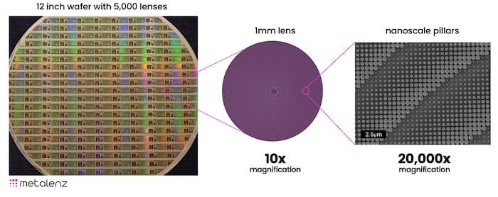
The critical factors for metalenses are not transistor density but subwavelength structural fidelity—feature linewidths, sidewall profiles, film-stack stability, and large-area pattern uniformity. Metalens meta-atoms (nanopillars or nanofins) typically fall within 40–100 nm for visible wavelengths and 80–200 nm for NIR. Research has further confirmed that visible-light metalenses can achieve minimum feature sizes below 50 nm. UMC’s 40 nm platform offers sufficient lithography resolution, alignment accuracy, film quality, and etch control to meet these requirements—without resorting to expensive, over-spec EUV nodes.
The key insight is this: metasurfaces requirelarge-area, highly regular, repetitive nanoscale arrays, a process profile that naturally aligns with the maturity, stability, and high yield of the 40 nm CMOS generation. Since entering mass production in 2008, the platform has accumulated extensive process know-how, equipment uniformity, and low defect density—precisely the foundational conditions for scaling meta-optics manufacturing.
Meanwhile, W2W bonding demands stringent control over planarity, overlay, and material-layer stability. Paradoxically, a mature node like 40 nm achieves higher bonding yields and lower process risk than advanced nodes. After all, metalenses are optical components rather than logic chips; their value lies instructural precision × large-area scalability × low cost × high consistency, not transistor-level linewidth scaling. Importantly, a CMOS “node” name does not represent the actual minimum printable feature size—40 nm platforms can reliably fabricate sub-50 nm meta-atoms after lithography and etch tuning, making them ideal for visible and NIR metalens production.
The UMC–Metalenz partnership thus marks the birth of the world’s first metasurface production line with trueCMOS-grade manufacturing scalability. With a mature process platform, 300 mm capacity, W2W integration, and sustainable expansion potential, UMC has become an indispensable manufacturing anchor within the global meta-optics ecosystem.
From an industry perspective, Taiwan—through the dual pillars of UMC and HHRI—has formed a complete chain spanning design, fabrication, packaging, and module-level integration. This positions Taiwan strategically across next-generation applications including CPO, optical I/O, AR/VR, 3D sensing, and wafer-level optics.
For Paid Member, SemiVision will discuss topics on
Technological Evolution and Industrial Applications of Metalenses:
A Comparative Analysis of Metalens vs. Microlens and COUPE Integration
Microlens (MLA) vs. Metalens: Operating Principles and Performance Differences
Process Comparison: From Glass Shaping to Nanopillar Arrays
Fabrication Methods for Metalenses
TSMC COUPE Platform and Metalens Integration
Role of Microlenses in COUPE
Role of Microlenses in COUPE (uLens Arrays)
Challenges of Nanopillar Structures
Metalenz and UMC Advance Polar ID Metalens Face-Recognition Module Into Mass Production, Opening a New Era of Low-Power, High-Security Biometric Sensing
Integration of Meta-Lenses with Silicon Photonics Platforms
Meta-Lens in Co-Packaged Optics (CPO)
Intra-Chip and Interconnect Meta-Lens Applications
Meta-Lenses in Optical I/O and Vertical Coupling
Fabrication Processes and Manufacturing Challenges of Meta-Lenses
IMEC: Advancing Optical Interfaces for Silicon Photonics and AR
MIT: Leading Innovations in Tunable and Ultra-Wide-Angle Meta-Lenses
Meta (Facebook): Toward Flat Optics for AR/VR Headsets
-
Metalens Interface Design on Silicon Photonic Chips
-
Integration Opportunities: Metalens in TSMC’s COUPE / CPO Platforms
-
High-Aspect-Ratio Nanopillars and the Process Limits of Dense Metasurface Patterns
Role and Capabilities of Taiwanese Companies(VisEra,AuthenX,Brillink.ai,Latitude Design Systems (LDS))
What Taiwanese Companies Must Strengthen to Enter Metalens + Silicon Photonics Manufacturing
Matching Metalens Processes to Silicon Photonics Flows
From Research Validation to Mass Production: Becoming Part of the Wafer-Level Optics Manufacturing Flow
Ecosystem and Collaboration Models
Metalens Commercialization Requires a Clear, Collaborative Value Chain
Future Opportunities: Differentiation Advantages Under Massive Market Potential
Finally, let’s address the question many people have been asking: What exactly is Himax’s strategy in metalens?
Technological Evolution and Industrial Applications of Metalenses:
A Comparative Analysis of Metalens vs. Microlens and COUPE Integration
From Snell’s Law to Planar Optics
Since Snell formulated the law of refraction in 1621, lenses have traditionally relied on curved glass or polymer surfaces to bend and shape light—a design approach that inherently leads to significant thickness and weight. The emergence of nanoscale fabrication and artificial electromagnetic materials in the 21st century paved the way for metamaterials and metasurfaces, dramatically expanding the degrees of freedom in optical wavefront control.
Microlens arrays (MLAs) can reduce lens size but still operate within the paradigm of refractive optics. Metalenses, by contrast, use subwavelength nanopillars or nanofins to modulate phase, polarization, and amplitude, enabling ultra-thin, planar, and multifunctional optical components. The following sections summarize the differences, fabrication pathways, and industrialization progress of both technologies.
Microlens (MLA) vs. Metalens: Operating Principles and Performance Differences
Fundamental Principles
Microlens Array (MLA):
MLAs rely on curved surfaces made of glass or polymers to generate optical path differences that focus incoming light—thus still obeying Snell’s law. Aberrations and focal length are determined by lens curvature, and typical thickness ranges from hundreds of micrometers to several millimeters. Literature indicates that microlens diameters are usually below 1 mm, fabricated through injection molding, thermal reflow lithography, or gradient-index layers. As dimensions shrink, diffraction must be taken into account.
Metalens:
A metalens consists of arrays of subwavelength nano-antennas (nanopillars or nanofins). By tuning the size, shape, and spacing of each meta-atom, one can manipulate propagation phase, geometric phase, or resonant phase, allowing the lens to achieve focusing entirely on a flat surface. Metalenses can simultaneously control phase, polarization, and amplitude, and can realize exotic functions such as negative refraction, zero refraction, and wavefront shaping.

Based on the differences above, metalenses hold significant advantages over microlenses in thickness, functionality, and integration. However, metalenses still face challenges in dispersion control and large-aperture fabrication, while microlenses—being mature and low-cost—remain the mainstream choice in many optical modules today.
Process Comparison: From Glass Shaping to Nanopillar Arrays
Fabrication Methods for Microlens Arrays
Photolithography and Thermal Reflow:
A 2D lithography step is first used to pattern cylindrical photoresist structures, which are then heated so that surface tension reshapes them into hemispherical lenses. The profile is subsequently transferred to the substrate via etching. This method supports batch fabrication but requires multiple lithography and dry-etch steps, making the equipment costly and the workflow complex.
Injection Molding / Embossing:
Liquid polymers are injected into a mold containing the lens profile and cured, enabling rapid, high-volume production of plastic microlenses. These methods require metal or silicon molds and demand precise temperature and pressure control. In multilayer or double-sided microlens arrays, mismatched thermal expansion of molds may cause alignment errors.
Gray-Scale Lithography and Direct Laser Writing:
A gray-scale mask is used to control exposure dose, forming a 3D lens surface in a single lithography step; alternatively, femtosecond-laser two-photon polymerization can directly write aspheric or free-form microlenses. These techniques offer high design flexibility but suffer from slow writing speeds and high costs, making them suitable for prototyping and precision optics rather than mass production.
Ultra-Precision Machining:
Single-point diamond turning or ball-end milling can directly machine optical materials, achieving surface roughness below 5 nm. However, this approach processes each lens individually, making it inefficient for large arrays, and it demands high-end equipment and tool stability.
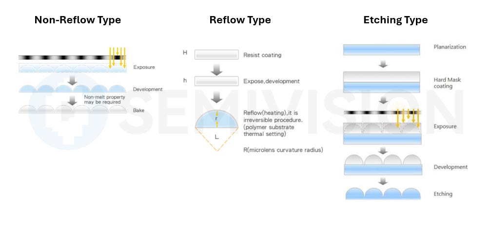
Source: Visera
Although these fabrication methods are mature, several pain points remain:
Double-sided microlensesin precision glass molding often suffer from alignment errors due to inconsistent thermal expansion of the molds, degrading optical performance.
Material thickness and surface profile are inherently limited, making it difficult to further reduce the thickness of optical modules.
The fabrication flow is fundamentally different from semiconductor processes, making co-fabrication with CMOS platforms difficult.
Fabrication Methods for Metalenses
Electron-Beam Lithography (EBL):
A focused electron beam writes patterns point-by-point and transfers them onto the substrate, enabling sub-10 nm features and high–aspect-ratio nanopillars suitable for high-NA metalenses. However, EBL is slow and expensive, making it unsuitable for large-area mass production.
Deep-UV Photolithography (DUV):
Using semiconductor-grade deep-UV projection lithography, patterns are transferred onto glass or wafers, followed by high–aspect-ratio dry etching to form nanopillars. This method enables metalenses with apertures larger than 10 cm. The Harvard team used this process to etch high-aspect-ratio nanopillars into glass, employing pattern stitching and vertical etching to create a 10-cm-diameter visible-light metalens—demonstrating that CMOS fabs can mass-produce large-format metalenses.

Nano-Imprint Lithography (NIL):
A master mold is first fabricated using EBL, then replicated onto polymers or photoresists via nano-imprint. High-index materials are subsequently deposited and etched to form nanopillars. NIL can pattern 65 nm features across 6–12 inch wafers, enabling high-volume, low-cost manufacturing. However, when producing high–aspect-ratio (HAR) nanopillars, traditional hard-PDMS molds introduce shear stress during demolding, causing structural collapse. Researchers have proposed using water-soluble PVA molds, which can be removed by wet etching to avoid shear stress, enabling defect-free HAR metalens fabrication.
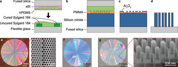
Two-Photon Polymerization and 3D Printing:
A tightly focused near-infrared laser induces two-photon polymerization in photoresists, allowing arbitrary 3D nanostructures with ~100 nm resolution. This approach is suitable for curved metalenses or fiber-tip metalenses, but point-by-point scanning makes it slow, and compatible materials remain limited.

Post-Etch Material Conversion:
Some methods oxidize silicon nanopillars into SiO₂, or directly deposit high-index materials such as TiO₂ or SiN followed by vertical dry etching to form nanopillars. These approaches closely resemble semiconductor dry-etch processes and can be integrated into CMOS fabrication flows.

In summary, metalens fabrication is highly compatible with semiconductor lithography and dry-etch technologies, making it feasible to scale production using existing wafer-fab infrastructure. However, manufacturing high–aspect-ratio nanopillars places stringent demands on lithographic resolution, etch verticality, and material selection—remaining a key bottleneck for full industrial mass production.
TSMC COUPE Platform and Metalens Integration
Overview of the COUPE Platform
At the TSMC Technology Symposium, this comprehensive diagram was presented to clearly illustrate — from a design perspective — how to define the significance of the COUPE platform.
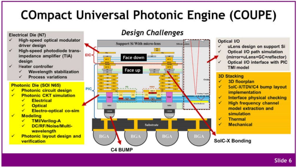
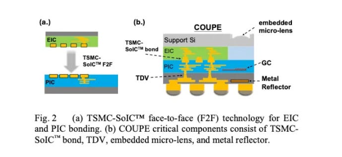
TSMC’s Compact Universal Photonic Engine (COUPE) is an optical–electronic engine designed for co-packaged optics (CPO), integrating electronic ICs (EICs) and photonic ICs (PICs) to minimize optical coupling loss. According to TSMC’s official research page, COUPE leverages EIC-PIC integration, solid-state structures, and SoIC face-to-face bonding to achieve extremely low grating-coupler and edge-coupler losses, and can be directly integrated into customer ASICs. As of early 2025, the first-generation COUPE design has completed development and entered validation, with mass production expected in the second half of 2026; the second generation is planned for production in 2027.
2025年6月25日
Role of Microlenses in COUPE (uLens Arrays)
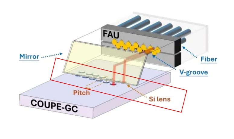
The COUPE optical engine must couple light from fibers or grating couplers into silicon photonic chips, and typically uses stacked glass microlens arrays as free-space coupling elements. These microlenses account for30–40% of module cost, requiring high-precision molds and multilayer stacking to reduce aberrations. Microlens arrays are a major cost driver in the coupling components for the first two COUPE generations and are expected to grow significantly as COUPE enters mass production in 2026–2028. However, microlens thickness and size increase overall module height and require mechanical alignment and bonding, which affects throughput and yield.
Prospects for Metalens Integration
TSMC’s optoelectronics subsidiary VisEra recently revealed plans to introduce metalens technology into CMOS image sensors (CIS) and micro-optical elements (MOE), particularly for AR glasses and smartphone imaging systems. VisEra stated that metalenses can significantly improve sensor light-collection efficiency and flatten optical stacks, with small-scale production expected in the second half of 2025.

In addition, VisEra and Artilux have developed a new silicon-based metalens module that uses wafer-level processing to overcome traditional packaging volume constraints, improving optical performance while achieving module miniaturization.
Artilux and VisEra Presenting Next-gen Si-based Metalens Technology
Potential Integration Pathways for Metalenses in COUPE
Although TSMC has not disclosed detailed design rules for metalens adoption within the COUPE platform, several foreseeable integration trends can be outlined:
Thickness and packaging advantages:
Metalenses are only a few hundred nanometers thick. Replacing microlens stacks could reduce COUPE module height and simplify co-packaging with ASICs.
Process compatibility:
COUPE relies on SoIC face-to-face bonding and wafer-level packaging. Metalenses can be etched or imprinted directly on wafers and potentially co-fabricated alongside silicon-photonics waveguides, eliminating alignment steps and meeting wafer-level integration requirements.
Improved coupling efficiency:
Metalenses can tailor phase profiles, providing beam shaping and achromatic behavior within a single layer. This may reduce coupling loss and improve bandwidth, though achieving large-aperture, broadband, achromatic metalenses remains challenging.
Adoption Timeline and Industry Impact
The transition from microlenses to metalenses in COUPE is likely to be gradual: metalenses may first be deployed in CIS and MOE modules, and once manufacturing matures, they may be integrated into the photonic engine itself.
Himax, currently a major microlens supplier, faces potential displacement or may need to pivot toward metalens production as the ecosystem shifts.
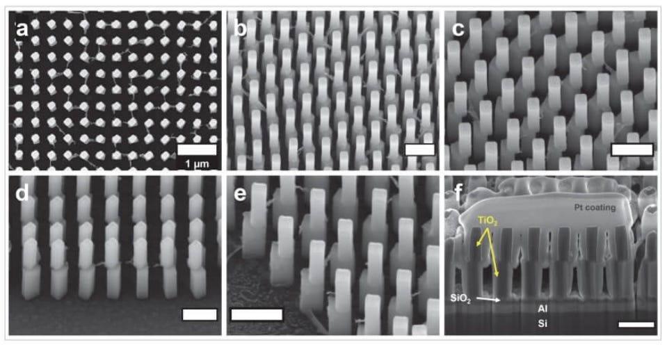
Challenges of Nanopillar Structures
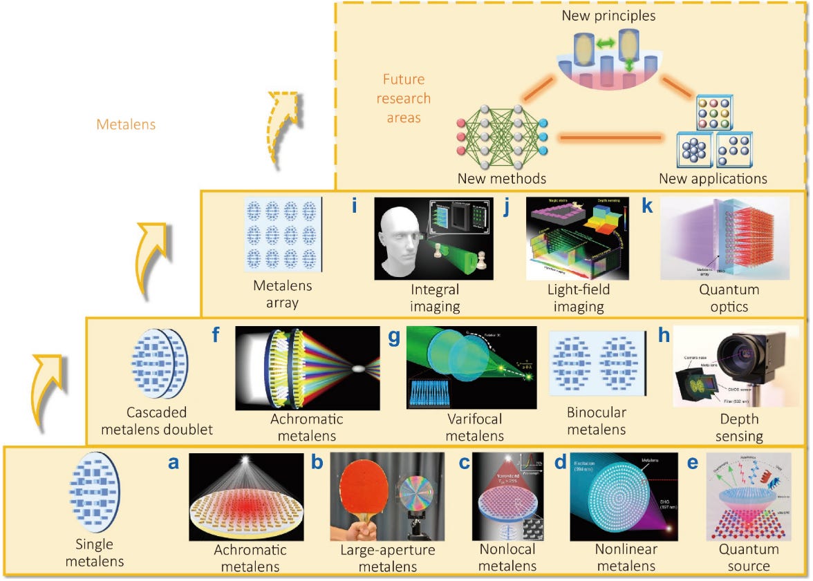
Source: oejournal.org
The performance of metalenses is highly dependent on the geometric dimensions and arrangement of individual nanopillars, leading to several key challenges:
Transmission and Phase Matching
An MDPI study reports that in propagation-phase metalenses, the transmission of nanopillars typically ranges from 60% to 100%. Variations in nanopillar size cause transmission inconsistencies, reducing overall lens throughput and degrading optical field uniformity. In addition, the actual phase often deviates from the theoretical phase by several tens of degrees, resulting in significant aberrations. The study showed that by increasing nanopillar transmission to above 0.95 and fine-tuning their positions, phase error can be reduced to 0.05°, dramatically improving focusing efficiency.
High–Aspect-Ratio (HAR) Fabrication Difficulty
Achieving a full 2π phase shift generally requires nanopillars with high aspect ratios. In conventional nano-imprint lithography, hard-PDMS molds generate shear stress during demolding, causing bending or breakage of HAR features. To address this issue, researchers proposed using water-soluble PVA molds that can be removed by wet etching, completely eliminating mechanical force during demolding and enabling defect-free HAR metalens fabrication. This demonstrates that mold materials and release methods critically affect metalens yield.
Pattern and Etch Uniformity
A metalens requires millions to billions of nanopillars across a wafer; any deviation in size or sidewall angle alters the effective refractive index, causing phase errors and reduced focusing efficiency. Deep-UV lithography and vertical dry etching help improve sidewall verticality, but pattern stitching and etch uniformity across large areas remain key challenges.
Material Selection and Loss
Early plasmonic metalenses suffered from high absorption losses. Modern designs employ dielectric materials such as TiO₂, SiN, or GaN to enhance transmission and thermal stability. However, the refractive index of these materials limits the achievable phase range, requiring increased thickness or modified cross-sections to obtain a full 2π phase shift—bringing the challenge back to high aspect ratios.
Large Apertures and Broadband Design
Most achromatic metalenses today have relatively small apertures. Designing broadband or wide-field metalenses often requires multilayer structures or hybrid phase mechanisms, increasing fabrication complexity. Additionally, nanopillar counts scale with the square of the aperture diameter, making manufacturing time and inspection cost major bottlenecks.
These challenges highlight that while metalenses offer tremendous potential, replacing microlenses at scale will require continued advances in materials, design algorithms, and high-volume manufacturing technologies.
Metalenses are transitioning from academic research to industrial applications, reshaping how optical components are designed and manufactured. Compared with microlenses, metalenses offer advantages such as extreme thinness, programmability, and CMOS-process compatibility, showing strong potential in smartphone cameras, AR/VR displays, depth sensing, biomedical endoscopy, and optical neural networks. However, challenges such as high–aspect-ratio nanopillar fabrication, phase and transmission errors, material losses, and large-aperture achromatic design still hinder large-scale commercialization.
TSMC’s COUPE platform currently relies on microlens arrays as its primary optical coupling elements, but companies like VisEra have already begun developing silicon-based metalens technologies to enhance sensor light-collection efficiency and reduce packaging thickness. In the coming years, metalenses are expected to achieve breakthroughs first in image sensors and miniature optical modules, and then gradually integrate into high-speed optoelectronic engines such as COUPE. With continued advancements in deep-UV lithography, nano-imprint processes, 3D nanofabrication, and AI-driven inverse-design algorithms, the cost and throughput of metalenses are expected to improve significantly, accelerating the optical IC revolution—transforming optics from thick to thin, and from curved to planar.
Metalenz and UMC Advance Polar ID Metalens Face-Recognition Module Into Mass Production, Opening a New Era of Low-Power, High-Security Biometric Sensing
UMC (United Microelectronics Corporation), a leading global semiconductor foundry, recently announced that it has partnered with Metalenz, the pioneer in metasurface optics, to bring the company’s innovative metalens-based facial recognition solution —Polar Face ID— into full mass production.
Industry’s First Polarization-Sensing Face Recognition Module
Polar ID is an ultra-compact, highly secure biometric module that uses polarization information for face recognition. The system integrates Metalenz’s polarization-sensitive meta-optic with advanced algorithms, enabling a single captured image to reveal far richer material and contour information. This deliversbank-grade facial authenticationwhile dramatically simplifying hardware architecture and reducing cost.
Metalenz has already demonstrated that its device can be directly integrated on top of image sensors within Snapdragon mobile platforms, highlighting its high system-level compatibility and low-power advantages. UMC provides its 40 nm CMOS platform and wafer-to-wafer (W2W) bonding technology to achieve high-yield, high-precision integration between the meta-optic and the CMOS sensor.
UMC Becomes a Key Global Manufacturing Partner
With advanced 12-inch wafer-fab capacity and a robust, high-quality supply chain, UMC not only supported Metalenz from pilot runs to mass production but is now a critical manufacturer for its next-generation polarization imaging modules.
Shih-chieh Hsu, VP of Technology Development at UMC, emphasized that the partnership began in 2021 and has continuously pushed metasurface optics toward commercial deployment. The successful mass production of Polar ID marks the emergence of UMC as a leader in next-generation imaging technologies.
Breaking the High-End Barrier and Enabling Market-Wide Adoption
Rob Devlin, CEO and co-founder of Metalenz, stated:
“Through our partnership with UMC, we are ready to bring Polar ID to the global consumer electronics market. This technology brings secure, affordable, and high-precision facial recognition to smartphones, wearables, and IoT devices — all within an extremely compact module.”
Compared with traditional face-recognition systems, Polar ID offers comparable or superior accuracy at lower cost and higher integration, enabling adoption in mid-range and entry-level devices. Potential applications include:
Smart door locks and home-security systems
Unmanned retail and payment terminals
Wearable medical and health-monitoring devices
Fast unlock and authentication for smartphones and tablets
Industry Significance and Future Outlook
The collaboration between UMC and Metalenz marks thefirst time metasurface optics has entered mass production for facial recognition at wafer scale, representing a major milestone with three key implications:
Planar optics enters mainstream CMOS manufacturing
Wafer-to-wafer bonding combines metalenses with sensors to achieve true wafer-level optical integration.
Miniaturization and standardization accelerate for biometric modules
Polarization information enhances recognition accuracy while simplifying optical paths and module structures.
A new market for secure, ubiquitous sensing emerges
Bank-grade face authentication can now expand beyond flagship phones into IoT and embedded devices.
As AI applications and security requirements continue to grow, the UMC–Metalenz collaboration model can extend to other sensing technologies, such as depth sensing, 3D imaging, structured light, and ToF modules — positioning metasurface optics as a foundational technology for next-generation smart devices.
Working Principles and Structural Design
Meta-lenses leverage subwavelength-scale artificial structures—known asmeta-atomsornanoantennas—engineered on a flat surface to achieve spatial phase control of incident light. While conventional refractive lenses rely on the optical path length within curved materials to produce phase delays, meta-lenses impose phase shifts directly at the interface by precisely arranging nanoscale elements across a planar substrate. Each nanostructure functions as a localized phase modulator: when light passes through, it experiences specific scattering and phase delay depending on the structure’s geometry, refractive index, and orientation.
To focus a planar wavefront, a meta-lens must emulate the parabolic phase profile of an ideal lens, where the optical path is shortest at the center and increases toward the edges in multiples of 2π. During the design process, engineers calculate the required phase compensation at each coordinate on the lens surface, and tailor the local nanostructure parameters to realize the target phase shift.
Phase Modulation Mechanisms
Propagation Delay (Waveguide-Type Phase):
Each nanopillar acts as a truncated waveguide, and the phase delay depends on its height and diameter. For instance, titanium dioxide (TiO₂) nanopillars with varying radii and heights can cover a full 0–2π transmission phase range while maintaining high efficiency. This method supports broadband performance but often requires high aspect ratio fabrication.
Geometric Phase (Pancharatnam–Berry Phase):
This technique utilizes the rotation of anisotropic structures, such as rectangular nanofins, to induce a phase shift. When circularly polarized light is incident, rotating the structure by an angle θ yields a 2θ phase delay. Meta-lenses designed with this approach often consist of silicon nanofins with smoothly varying orientations, ideal for polarization-sensitive applications.
Resonant Phase (Huygens’ Metasurfaces):
Based on Mie resonances, certain dielectric nanostructures (e.g., nanodisks) exhibit sharp phase changes near resonant frequencies. Huygens-type meta-lenses use both electric and magnetic dipole resonances to achieve complete 2π phase control while ensuring high transmission. This technique reduces the required structure height but tends to be more narrowband and sensitive to fabrication tolerances.
Each approach offers trade-offs: geometric phase lenses are simple and polarization-dependent, propagation-type lenses support broadband operation but demand more complex fabrication, and resonant-based lenses offer compactness but require precise tuning and suffer from narrower bandwidths.
Material Considerations
Material selection is crucial to achieving the desired optical phase delay within ultra-thin layers. The material must exhibit a high refractive index and minimal absorption loss at the target wavelength. Some commonly used materials include:
Titanium Dioxide (TiO₂)andGallium Nitride (GaN):
Ideal for visible wavelengths due to their high refractive indices (~2.4) and excellent transparency.
Crystalline or Amorphous Silicon (Si/a-Si):
Widely used in the near-infrared domain, particularly around 1.3–1.55 µm for telecom applications, due to their high index (~3.5) and CMOS compatibility.
Aluminum Nitride (AlN)andHafnium Oxide (HfO₂):
Suitable for ultraviolet (UV) applications, combining high refractive index and transparency.
Fabrication compatibility is also a key consideration. While materials like TiO₂ are not native to standard CMOS processes, they can be deposited as thin films on glass or silicon wafers and patterned via electron-beam lithography or nanoimprint techniques. Silicon, on the other hand, benefits from full integration with standard semiconductor manufacturing, making it ideal for monolithic integration with photonic circuits.
Meta-lenses represent a paradigm shift in optical design by enabling arbitrary wavefront shaping on a flat surface. Through precise nanostructure engineering, they offer compact, lightweight, and high-performance alternatives to conventional optics. In addition to enabling high numerical aperture focusing, meta-lenses can perform advanced functions such as polarization control, multi-focus generation, and exotic beam shaping—capabilities traditionally unattainable with standard lenses.
By fundamentally decoupling optical function from bulk geometry, meta-lenses pave the way for ultra-compact and highly integrated optical systems, with transformative potential across imaging, sensing, and communication technologies.
Performance Comparison and Advantages over Traditional Microlenses
Thickness and Form Factor
One of the most prominent advantages of meta-lenses is their ultra-thin, planar architecture. Typical meta-lenses measure only tens to hundreds of nanometers in thickness—on the order of the operating wavelength—whereas traditional microlenses can be several microns to even millimeters thick. For example, a metalens based on a nanostructured TiO₂ film may be just ~100 nm thick, while an equivalent diffractive optical element (DOE) might require ~1 µm thickness, and conventional molded glass lenses may exceed several millimeters.
In addition to being thin, meta-lenses can be fabricated directly on CMOS wafers or glass substrates, significantly reducing system volume and weight. This enables monolithic integration with image sensors and photonic chips without the need for discrete lens assembly, lowering packaging complexity and enhancing robustness. Their compactness and on-chip manufacturability make meta-lenses ideal for mobile, wearable, and embedded optical systems.
Focusing Efficiency and Optical Quality
In theory, meta-lenses can achieve diffraction-limited focusing performance, as their engineered phase profiles can correct for various aberrations with nanometer-scale precision. However, one historical challenge has been the actualtransmission efficiencyof meta-lenses. Losses from scattering, material absorption, and fabrication imperfections have limited earlier metalens efficiencies to only 20–80%, depending on design and wavelength regime.
In contrast, traditional refractive lenses with anti-reflective coatings can routinely reach transmission efficiencies of 97–99%. That said, recent advances in fabrication fidelity, nanostructure design, and high-index dielectric materials have significantly improved meta-lens efficiency. A 2024 study demonstrated a meta-lens with 92% focusing efficiency at NA = 0.24, approaching theoretical predictions.
The remaining performance gap is largely attributed to process-induced deviations in nanostructure geometry. As manufacturing processes such as electron-beam lithography, nanoimprint, and deep-UV lithography continue to improve, the experimental performance of metalenses is rapidly converging with simulations.
Chromatic Aberration and Dispersion Control
Due to their diffractive nature, meta-lenses exhibit strong wavelength dependence—their focal length shifts with incident wavelength, similar to diffractive optical elements. This chromatic aberration presents a fundamental challenge, especially for broadband or full-color imaging applications. While traditional refractive optics mitigate chromatic effects using multi-element achromatic lens assemblies, meta-lens researchers are pursuing several novel approaches:
Dispersion-engineered unit cells:Tailoring nanostructure geometries to provide wavelength-dependent phase shifts, enabling achromatic focusing across a band of wavelengths.
Multilayer stacking:Vertically stacking multiple metasurfaces to independently tune phase profiles at different wavelengths.
Lateral multiplexing:Segmenting the lens into sub-regions optimized for specific spectral bands.
Each method comes with trade-offs. For example, multilayer designs increase fabrication complexity, and lateral multiplexing may lower spatial resolution. Nonetheless, metalenses achieving near-diffraction-limited achromatic focusing from 400–660 nm using GaN nanostructures have been experimentally demonstrated, suggesting real-world feasibility is within reach.
Aberration Correction and Multi-Functional Integration
Meta-lenses offer significantly greater degrees of freedom than traditional optics when it comes to wavefront shaping. Instead of being limited by the geometry of curved surfaces, designers can precisely engineer the phase, amplitude, and polarization response of each meta-atom on the lens surface.
This allows for simultaneous correction of multiple monochromatic aberrations—such as astigmatism and coma—on a single flat layer. Furthermore, meta-lenses can supportmulti-functionality: a single device may perform polarization-selective focusing, generate vortex beams, or act as a filter and beam splitter, all within one layer.
One commercial example is Metalenz’s infrared imaging metalens, which combines focusing, filtering, and beam-shaping functions into a single metasurface—replacing multiple discrete components in a conventional optical stack.
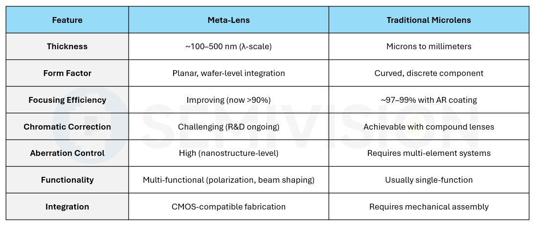
Compared to traditional microlenses, meta-lenses deliver unmatched advantages in thickness, weight, integration capability, and design flexibility. Their compatibility with semiconductor manufacturing enables direct on-chip deployment, paving the way for ultra-compact optical modules in smartphones, AR/VR headsets, biomedical sensors, and more.
Although challenges such as chromatic aberration and high-NA efficiency persist, rapid advancements in nanofabrication and materials science are steadily overcoming these limitations. As a result, meta-lenses are poised to not only complement but potentially replace conventional lenses in next-generation optical systems.
Integration of Meta-Lenses with Silicon Photonics Platforms
Silicon photonics platforms integrate optical components—such as waveguides, modulators, and photodetectors—directly onto silicon chips, enabling high-speed optical communications and on-chip photonic computing. However, one of the persistent challenges in silicon photonics is the efficient coupling between on-chip waveguides and external optics such as optical fibers or free-space beams. Due to the submicron cross-section of silicon waveguide modes, direct coupling to fibers results in significant mode-size mismatch and demands extremely precise alignment, often requiring complex coupling structures.
Meta-lenses offer an innovative solution to this bottleneck. Their planar geometry allows for fabrication directly on the chip surface and precise tailoring of wavefronts, enabling them to function as mode converters, collimators, and focusing elements. Specifically, meta-lenses can expand and collimate the highly divergent output beams from silicon waveguides or focus free-space light into waveguide inputs, improving mode matching and alignment tolerance.
Meta-Lens in Co-Packaged Optics (CPO)
In co-packaged optics (CPO), processors or switch ASICs are tightly integrated with optical engines. Traditional fiber coupling techniques using ball lenses or microlens arrays face significant limitations due to strict alignment tolerances and confined packaging space. Meta-lenses, on the other hand, can be monolithically integrated on-chip as optical interfaces to enhance coupling efficiency and increase positional tolerance.
For instance, the “Photonic Bump” concept proposed in industry combines a broadband metasurface deflector and micro meta-lens into a flat optical interface. This structure can deflect and expand the beam emitted from a silicon waveguide, increasing the beam diameter to several tens of microns. As a result, fiber alignment tolerance improves from ±2–3 µm to over ±30 µm, with only a minor loss penalty (~0.5 dB). Such enhancements dramatically simplify high-density optical I/O assembly in CPO environments.
Custom-designed meta-lenses can be placed directly above output grating couplers or facet-coupled waveguides, functioning as beam expanders, focusing lenses, or polarization controllers—delivering robust, multi-channel optical coupling with relaxed alignment requirements.
Intra-Chip and Interconnect Meta-Lens Applications
Recent research demonstrates meta-lens functionality for on-chip beam transformation. One study used a freeform-optimized silicon meta-lens on a standard SOI chip to bridge a wide waveguide to a narrow one over just a few microns. Measuring only 2.35 µm × 2.35 µm, the device achieved a high numerical aperture (NA = 2.03) and performed an 11× mode diameter transformation over a sub-10 µm propagation length. Forward coupling efficiency exceeded 96%, effectively replacing long tapered waveguides (often >100 µm) with ultra-compact structures.
In chip-to-chip free-space optical interconnects—envisioned as a future replacement for bandwidth-limited electrical interconnects—each communication channel requires collimation and focusing optics. Meta-lens arrays fabricated directly on transmitter and receiver chips can serve as compact beam expanders and focusers. Their lithographic customizability allows for dense, multi-channel parallelism, essential for scaling optical interconnect bandwidth. Furthermore, meta-lenses’ planar profile makes them inherently compatible with integration alongside VCSELs, PDs, and silicon waveguides without the need for discrete lens alignment.
Meta-lenses can also be transferred onto optical fiber tips, enabling fiber connectors to perform advanced beam shaping or focusing functions. For example, gold nanostructure arrays fabricated on silicon wafers have been successfully transferred to fiber end-faces, converting conventional fibers into meta-fiber interfaces. Such methods offer a scalable way to mass-produce lens-integrated optical fibers from wafer-level metasurface templates.
Meta-Lenses in Optical I/O and Vertical Coupling
In optical I/O systems, meta-lenses can enhance the connection between photonic chips and either fibers or free-space optics. Traditional grating couplers suffer from wavelength sensitivity and narrow angular bandwidth. Meta-lenses, however, can be designed to maintain consistent beam direction and profile over broad wavelength ranges, making them ideal for wideband vertical coupling.
Startups likeTeramounthave already demonstrated “optical bumps” that integrate metasurface lenses and deflectors into the wafer-level fabrication process. These components not only reduce alignment sensitivity and increase bandwidth but also allow for detachable interfaces in co-packaged systems. By embedding broadband meta-optical elements directly into photonic IC packaging, such designs open the door to modular, scalable, and high-density optical interconnects.
Meta-lenses present a compelling solution to one of silicon photonics’ most persistent challenges: efficient and scalable optical coupling. Their planar, customizable nature enables high-performance mode conversion, relaxed alignment tolerance, and dense optical I/O integration—all without increasing footprint or assembly complexity.
Fabrication Processes and Manufacturing Challenges of Meta-Lenses
Overview of Fabrication Process
Meta-lens fabrication primarily relies onplanar semiconductor processes, similar to those used in integrated circuits (ICs) and MEMS, but requiringnanometer-level patterning precision. The general workflow involves:
Material Deposition: A high-refractive-index thin film (e.g., TiO₂, Si) is deposited on a substrate such as glass or silicon.
Pattern Definition: Nanostructures are defined usingelectron beam lithography (EBL)or advanced photolithography:
EBLenables direct, high-resolution “write-by-point” nanopatterning, suitable for prototyping or master mold fabrication. However, it is slow and expensive, thus unsuitable for mass production.
Deep UV lithography (DUV)struggles with sub-100 nm resolution due to diffraction limits, althoughEUV lithographyshows promise for future metasurface production.
Nanoimprint Lithography (NIL)has emerged as ascalable, cost-effective alternativefor large-area fabrication. It uses a hard mold—typically fabricated via EBL—to stamp nanostructures onto a UV-curable polymer. After curing, the pattern is transferred to the substrate, enabling rapid replication with high fidelity.
Replication Workflow:
A master pattern is created via EBL and transferred to the high-index material using dry etching.
Astamp moldis replicated from the master using materials like PDMS or OrmoStamp with anti-adhesion coatings.
The mold is used to replicate the structures on target substrates via UV-NIL, followed by optional etching to transfer the patterns into the final optical layer.
This“master mold-to-replica” paradigmenables cost-effective scaling: a single EBL master can be reused thousands of times. NIL has successfully produced high-qualityinfrared meta-lenses on 6–12 inch wafers, and even integration into CMOS-compatible photonic processes has been demonstrated.
Transfer Printing Techniques
In applications where meta-lenses need to be placed onnon-planar or flexible substrates—such as curved optics, fiber tips, or image sensor surfaces—transfer printingbecomes valuable.
Sacrificial Layer Release: Nanostructures are fabricated on a donor substrate with a sacrificial layer, then released.
Pick-up and Transfer: A soft elastomeric stamp (e.g., PDMS) picks up the structure and transfers it to the target substrate using controlled adhesion.
Use Cases:
Meta-lenses transferred tooptical fiber facetsfor integrated focusing tips.
Meta-lenses printed onstretchable substratesfor tunable focal length under strain.
Direct bonding ontoCMOS sensorsfor ultra-compact proximity optics.
Transfer techniques greatly increase versatility, enabling hybrid packaging strategies and facilitating integration with conventional optical systems.
Manufacturing Challenges in Metalens
Despite leveraging established micro/nano fabrication technologies, producing high-performance, high-volume meta-lenses involves several key technical hurdles:
- Precision and Yield
Meta-lenses often require billions of nanoscale elements withnanometer-level dimensional accuracyto ensure phase fidelity. Variations in structure dimensions—even a few nanometers—can degrade optical performance due to accumulated phase errors.
Etching control,resist profile optimization, andprocess uniformityacross the wafer are essential.
Statistical process control and real-time metrology are needed to maintain yield in large-scale manufacturing.
- High Aspect Ratio Structures
To achieve full 0–2π phase shifts (especially for propagation-phase meta-lenses in the visible regime), nanostructures often requiretall pillars (>500 nm)with narrow lateral widths (<100 nm), resulting inhigh aspect ratios (>10:1).
These structures are susceptible tosidewall roughness, tapering, or collapseduring etching.
Advanced plasma etching techniques, such ascryogenic or Bosch DRIE, combined withhard mask layers, are being adopted to fabricate vertical, high-fidelity pillars.
Recent studies have achieved10:1 aspect ratio silicon nanopillarsusing optimized low-temperature processes, but repeatability and process robustness remain ongoing challenges.
- Large-Area, High-Complexity Patterns
Applications such as VR/AR optics may require meta-lenses spanningcentimeter-scale diameters, containingtens of billions of unique nanostructures.
Even with scalable methods like NIL,defect controlbecomes critical.
Common issues includesticking during mold release, resulting in incomplete patterns.
To mitigate this, anti-sticking coatings (e.g., fluorinated silanes) are applied to molds, but wear and tear over multiple uses can degrade fidelity.
Regularmold refurbishment and inspection routinesare essential in production lines.
- Material Compatibility and Packaging
Many high-performance meta-lens materials (e.g., TiO₂, GaN) are not standard in CMOS fabs and require:
SpecializedALD or sputtering deposition.
Custom etch chemistries.
Attention tostress, contamination, and CMP compatibility.
Paradoxically, the thin nature of meta-lenses makes themmore CMOS-friendlythan large DOEs, as they avoid deep silicon etching. However,encapsulation is neededto protect delicate structures from dust, abrasion, or environmental degradation.
A common solution isadding a protective glass or polymer capping layer, but this alters the optical environment and must be factored into design (e.g., the refractive index change modifies phase delay).
Properco-design of meta-lens + packagingis essential for consistent field performance.
Meta-lens fabrication is grounded in mature semiconductor technologies but still requires advances inpatterning accuracy, process integration, throughput, and defect controlto become commercially scalable.
Encouragingly, industry momentum is building:
NIL and wafer-level meta-lens integration are gaining traction.
Companies likeMetalenzhave proven that metasurfaces can be mass-produced using standard semiconductor equipment.
The future may see dedicated“meta-optics foundries”and the development ofstandardized manufacturing platformsfor scalable planar optics.
As interest in wafer-level optics grows—particularly for applications like smartphone sensors, AR displays, and silicon photonics—meta-lens manufacturing will become a central pillar in next-generation optical design and fabrication.
Real-World Applications and Emerging Research Trends
In recent years, meta-lens technology has begun to transition from academic laboratories to real-world applications. Major research institutions and companies are increasingly investing in metasurface optics, leading to significant breakthroughs across multiple sectors. Below are several representative cases and trends that illustrate the technology’s momentum:
IMEC: Advancing Optical Interfaces for Silicon Photonics and AR
IMEC, Europe’s leading nanoelectronics and photonics research center, is actively exploring next-generation optical I/O and co-packaged optics (CPO) interfaces. While many of their public efforts focus on silicon nitride and polymer waveguide couplers (e.g., using anti-etch back teeth converters to enhance fiber coupling), these structures still suffer from mode size mismatches and tight alignment tolerances—precisely the challenges meta-lenses are well-suited to solve.
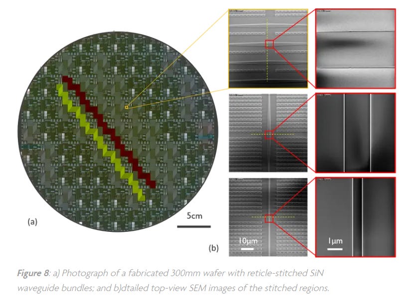
Interfacing silicon photonics for high-density co-packaged optics
Though IMEC has yet to fully disclose meta-lens projects, it is plausible they are evaluating flat optics for broadband optical I/O. For example, planar micro-lens arrays fabricated on optical interposer layers, or metasurface optics integrated into pluggable interconnects, could greatly ease fiber alignment. IMEC has also publicly forecasted that by 2035, AR glasses will rely heavily on flat optics to reduce volume and improve power efficiency—an area where meta-lenses could play a critical role.

2025年11月12日
MIT: Leading Innovations in Tunable and Ultra-Wide-Angle Meta-Lenses
Researchers at the Massachusetts Institute of Technology (MIT) have pioneered numerous innovations in metasurface optics. One notable development is adynamically tunable meta-lensusing GST (Ge-Sb-Te) phase-change materials. This lens can adjust its focal length via thermal modulation, without any mechanical movement, opening the door to compact zoom capabilities for drones, smartphones, and other imaging systems.

Another collaborative study between MIT and UMass Lowell demonstrated anultra-wide-angle “fish-eye” meta-lenscapable of 180° panoramic imaging on a single flat substrate—eliminating the bulk of conventional fisheye assemblies. MIT researchers have also advanced computational design methods, leveraging machine learning and inverse design algorithms to rapidly optimize nanostructure layouts. These achievements highlight MIT’s leadership in both static and reconfigurable metasurfaces, laying the groundwork for software-defined optical components.
Meta (Facebook): Toward Flat Optics for AR/VR Headsets
Meta’s Reality Labs have expressed strong interest in next-generation optics for augmented and virtual reality (AR/VR). While they haven’t publicly released metalens-equipped products, signs of involvement are emerging. At CES 2024, Korea-based P&C Solution showcased a device called“METALENSE 2”—an XR headset explicitly referencing metasurface technology for outdoor AR displays, possibly marking the first near-eye meta-lens implementation.
Meta’s published roadmaps emphasize holographic waveguides, polarization optics, and metasurfaces as key enablers of compact AR headsets. Meta-lenses are well-positioned to function as eyepieces or compact imaging elements, replacing traditional lens stacks to reduce system size and weight. Furthermore, their flat nature benefits embedded sensing modules (e.g., gesture tracking, 3D sensing) by minimizing camera module thickness. Meta’s 2023 acquisition ofLuxexcel, a 3D-printed optics company, also hints at the convergence of additive manufacturing and metasurface integration for mass production of advanced optical components.

2025年11月6日
Rockley Photonics: Wearable Health Sensors and Optical I/O
Rockley Photonics, known for silicon photonics-based wearable biosensors, integrates multiple lasers and detectors on-chip for non-invasive blood analysis. While the company has not publicly confirmed the use of metasurfaces, their applications—such as beam expansion for skin illumination or signal collection from diffuse reflections—could greatly benefit from meta-lens integration.
In machine vision and data communications, Rockley’s ongoing development of high-density optical I/O modules could also leverage meta-lenses to enable free-space chip-to-chip links or efficient coupling into multi-core fibers. As a pioneer in silicon photonics, Rockley is likely to explore metasurfaces as a path to increase integration, reduce packaging complexity, and enhance system performance.
Metalenz: The First Commercial Success Story
Spun out of Harvard University’s Capasso Group,Metalenzis the first startup to commercialize meta-lens technology. In 2022, Metalenz partnered with STMicroelectronics to integrate metasurfaces intoTime-of-Flight (ToF)depth sensors (VL53L8), enabling mass production of meta-lenses for consumer electronics. These planar optics replaced traditional multi-element lenses, reducing module size while improving light collection efficiency and reducing power consumption.
Metalenz lenses are fully flat, single-layer optical devices fabricated at the wafer level, co-manufactured with semiconductor components. In ST’s infrared depth sensor, a single meta-lens performs both focusing and wavefront shaping—functions typically requiring multiple discrete lenses—with a thickness of just a few microns. The ability to “print” optics in semiconductor fabs demonstrates unprecedented scalability.
Encouraged by Metalenz’s success, smartphone OEMs and sensor makers are evaluating meta-lenses for applications such as 3D sensing, face recognition, and ultra-thin cameras. Millions of Metalenz lenses are expected to ship in the coming years, signaling a major milestone in planar optics commercialization.
Global Trends and Other Research Efforts
Beyond the aforementioned leaders, numerous institutions continue advancing the meta-lens frontier:
Harvard University: Developing multi-layer stacked meta-lenses for enhanced phase control and broad spectral coverage.
Doubling down on metasurfaces-Bilayer device can control many forms of polarized light
Korean and Chinese research groups: Demonstrating large-area flat lenses (e.g., 100 mm diameter visible-light metalens arrays) and system-level integration for imaging and LiDAR.
Infrared and LiDAR systems: Researchers are exploring meta-lenses for high-NA, large-aperture infrared imaging, aiming to miniaturize thermal cameras and automotive sensors.
NIL Technology (Denmark): Offering nanoprintable meta-lens samples and tooling solutions to help companies adopt metasurface optics for eye tracking, depth sensing, and AR/VR modules.
Sunny Optical and other optical component giants: Initiating flat optics development programs to stay ahead of the curve.
Standards bodies (e.g., SPIE): Actively discussing standardized metrics for meta-lens characterization, such as focal length, modulation transfer function (MTF), and environmental stability, to facilitate broader adoption.
From Lab to Market in Metalens
Meta-lens technology is rapidly maturing, transitioning from research prototypes to scalable, commercial-grade solutions. The success of Metalenz’s smartphone depth sensor, the integration efforts by major players like Meta, MIT’s dynamic lens research, and the emergence of standards all suggest a technology nearing its tipping point.
In the coming years, we expect to see meta-lenses integrated across diverse domains—from ultra-thin smartphone cameras and AR glasses to LiDAR sensors, medical imagers, and chip-scale optical I/O. The convergence of academic innovation, industrial scaling, and ecosystem collaboration is accelerating this transition—bringing flat optics from concept to mass deployment.
Technical Challenges and Future Development Potential
Despite the promising outlook of meta-lens technology, several key challenges must be addressed before it can fully replace or be widely deployed across diverse optical systems.
Broadband Achromatic Performance
As discussed earlier,chromatic dispersionis an intrinsic challenge of metasurfaces. While most meta-lenses perform well under monochromatic illumination, their performance significantly degrades under broadband light such as natural white light. The focal length varies with wavelength, making it difficult to form sharp images across the spectrum. Though several demonstrations of broadband or multi-band metalenses have been reported, they often suffer from efficiency trade-offs.
Achieving performance comparable to traditional achromatic doublets will requiremore complex architectures—multi-layer stacking, hybrid materials, or the combination of multiple dispersion-engineering strategies. These approaches, however, introduce new fabrication challenges such as precise layer alignment and increased process complexity. Future directions may include:
Developingnew high-dispersion materialsor metamaterials.
Applyingmachine learning algorithmsto optimize nanostructure geometries for phase control across multiple wavelengths.
Implementingactively tunable mechanisms(e.g., electro-optic or thermo-optic control) to dynamically compensate for chromatic shifts.
Solving chromatic aberration will unlock applications such asbroadband imaging, enabling meta-lenses to be used in smartphone cameras and full-color AR displays.
Efficiency Optimization
Although recent experimental meta-lenses have achieved>90% focusing efficiency, many high-performance systems require transmission efficiency approaching that of traditional optics—97–99%. Losses arise from bothmanufacturing imperfectionsandinherent design constraints. For instance:
Pancharatnam-Berry phase-based metalenses are optimized for circular polarization and may underperform under linearly polarized light.
Huygens-type surfaces exhibit strong wavelength dependence, with efficiency dropping off sharply outside their design wavelength.
Future improvements may involve:
Multi-resonant unit cellsthat sustain high efficiency across broader spectral ranges.
Hybrid phase control mechanisms(combining propagation, geometric, and resonant phases).
Low-loss materialsfor mid-IR and UV regimes, where intrinsic absorption currently limits performance.
Moreover, as nanofabrication technologies advance toward the2 nm semiconductor node, the precision and fidelity required for high-efficiency metasurfaces will become increasingly accessible, closing the gap between theoretical and real-world performance.
Standardization and Manufacturability
Today, most meta-lens designs are custom-developed and lack standardized design toolchains or process flows. To accelerate adoption, the industry must develop:
Standardized optical performance metrics(e.g., focal length, NA, off-axis aberrations, polarization sensitivity).
Fabrication tolerance benchmarksto assess performance degradation.
Interface standardsfor mechanical, optical, and electrical integration with existing systems.
Mass manufacturing also needs to evolve. While techniques likenanoimprint lithographyandstepper-based projection lithographyoffer promise, scaling will benefit from:
Roll-to-roll imprintingfor large-area planar optics.
Wafer-level productionof metasurfaces, as pioneered byMetalenz, which demonstrated the feasibility of mass-producing meta-lenses in semiconductor fabs.
A long-term vision is the emergence of“Optics PDKs” (Process Design Kits)that allow engineers to design meta-lenses like ICs, while fabs handle the fabrication—ushering in an era of“chip-like lens manufacturing.”
System Integration and Alignment
Although meta-lenses are inherently planar and compatible with wafer-level integration,system-level alignmentremains a challenge in certain use cases. For example:
In smartphone camera modules, meta-lenses may still need to be packaged at a specific distance from the image sensor to establish focal length, requiring tightalignment tolerances.
However, compared to multi-element lens stacks, single-layer meta-lenses significantly simplify assembly, especially when combined withwafer bonding techniques.
Emergingwafer-to-wafer alignment and stacking technologiesallow precise bonding of lens wafers with CMOS sensor wafers at the 12-inch wafer scale. This means optical and electronic components no longer need to be monolithically fabricated—they can be independently optimized andintegrated post-fabrication.
Meta-lenses’ polarization sensitivity—particularly in geometric-phase-based designs—introduces another consideration. Optical systems may needadditional polarization components(e.g., polarizers or quarter-wave plates) orpolarization-insensitive designsusing complementary structural arrangements. Though it adds complexity, polarization management is common in modern optics and can be engineered into the system architecture.
Material and Environmental Stability
Long-term durabilityof nanostructured meta-lenses under environmental conditions is critical. While materials likeTiO₂, SiO₂, and GaNare chemically stable, exposure to humidity, heat, and intense illumination—especially inhigh-power laser systems—can cause structural degradation (e.g., thermal deformation or melting).
For flexible electronics,mechanical reliabilityof metasurfaces under repeated bending must also be validated. Potential solutions include:
Protective coatingsand rounded nanostructures to mitigate stress concentration.
Material optimization, such as etching silicon metasurfaces onto fused silica substrates for ultra-high durability.
In most consumer applications (smartphones, AR headsets), environmental demands are moderate, and current materials suffice. However,automotive(outdoor temperature swings) andaerospace(radiation, vacuum) deployments will require rigorous material and system-level engineering.
Future Potential and Industry Impact
Once these challenges are overcome, meta-lenses are poised to revolutionize multiple industries:
Consumer electronics: Enabling thinner smartphone camera modules, eliminating camera bumps, and improving 3D sensing and AR projection systems.
AR/VR headsets: Acting as lightweight, full-color imaging optics to replace bulky conventional lens stacks. Meta-lenses may work in conjunction with waveguides to deliver wide-FOV, high-efficiency virtual images directly to the eye.
LiDAR and robotics: Facilitating low-cost, planar beam emitters and detectors, improving reliability, and reducing package size.
Medical imaging and lab-on-chip systems: Allowing miniaturized endoscopes, spectral cameras, and microscope objectives; enabling on-chip optical readout for biosensors.
Reconfigurable optics: Integrating meta-lenses with MEMS, liquid crystals, or phase-change materials to enable electrically tunable focusing, beam steering, and programmable lensing—creating flat zoom lenses without moving parts.
In short, meta-lenses could becomefoundational building blocksof future optical systems. Their flat form factor and unprecedented control over light propagation are ushering in a shift“from bulky to flat, from curved to planar”in optical design and manufacturing.
Meta-lenses have rapidly progressed from academic curiosities to viable components in real-world applications. Today, they stand at the threshold of commercial maturity. Once key technical hurdles—especially in chromatic control, efficiency, and manufacturing—are resolved, meta-lenses are set to becomeas ubiquitous in optics as ICs are in electronics.
From smartphones to spacecraft, meta-lenses hold the potential to redefine how we design, fabricate, and interact with light-driven technologies. The optical revolution is flattening—and meta-lenses are leading the way.
Finally, we examine several key topics in depth
- Metalens Interface Design on Silicon Photonic Chips
Silicon photonic chips have long faced a fundamental challenge in opticalcoupling: how to efficiently convert the extremely small guided modes inside silicon waveguides into much larger free-space or fiber modes, while minimizing loss and beam divergence. Conventional techniques—such as inverse tapers, grating couplers, and microlens-fiber assemblies—can achieve mode matching, but each comes with trade-offs in efficiency, bandwidth, polarization sensitivity, or footprint.
The rise ofmetalensesopens a new design paradigm for silicon photonic chip interfaces: by patterning subwavelength nanostructure arrays directly on the chip surface, one can perform mode conversion and wavefront shaping in an ultra-compact footprint. A metalens is essentially a metasurface comprised of dense arrays of subwavelength “nanopillars” or “nano-grooves” that precisely manipulate the phase, amplitude, and polarization of light. On a silicon-photonics platform, this means a metalens can serve as a miniaturemode converter, expanding, collimating, or reshaping the guided mode into a form more suitable for free-space propagation or fiber coupling.
Metalens as a Mode Converter: Opportunities and Examples
When light exits a silicon waveguide into free space, the aperture mismatch relative to fiber modes typically leads to severe divergence and mode mismatch. Integrating a metalens directly at or near the waveguide facet enables immediate wavefront reshaping.
One notable example embeds a planar metalens inside an SOI chip to maintain high modal quality across a sharp waveguide width transition. By patterning a sequence of rectangular nano-features at the interface between wide and narrow waveguides, the structure focuses light from an 11 µm-wide mode into a 1 µm-wide mode with96% forward transmission efficiencyat 1550 nm. In the reverse direction, the metalens collimates the diverging field, maintaining~69% TE₀ transmission, demonstrating its ability to performultra-short-range mode conversionwith focal lengths on the order of 10 µm.
Traditional inverse tapers require hundreds of microns to smoothly transform large mode-area differences. Shortening the taper results in inadequate wavefront evolution and added phase errors. A metalens, however, can correct the wavefront at the nanoscale to create a quasi-planar phase front within just a few microns.
Further research has produced all-dielectric metalenses implemented directly on 220 nm-thick SOI waveguides. One demonstrated a10.5 × 2.5 µm²on-chip metalens achieving90% focusing efficiency, showing the feasibility of highly compact and high-performance mode converters.
Nanopillar Layout: Mode Conversion and Scattering Compensation
The performance of a metalens depends on careful design of each nanopillar (or slot), acting as a subwavelength “antenna” that modulates local phase and amplitude. Designers typically start with a target phase profile—such as a parabolic wavefront for focusing—and map each phase location to a specific nanopillar geometry.
Because silicon waveguide modes are tightly confined, the metalens must create strong phase gradients to reshape the beam. This is achieved via varying pillar sizes, shapes, and spacing. In SOI examples, rectangular slot arrays modulate phase accumulation along the propagation direction.
However, local-phase approximations often fail because metalens arrays are finite and non-periodic—strong inter-cell coupling occurs. To address this, researchers increasingly usetopology optimizationto jointly optimize all unit cells. A 2025 study combined pre-optimized metalens structures with global topology optimization to reach93.7% transmission efficiencyin a compact20 × 12 µm²device.
Minimizing scattering losses is equally important. Designers may choose:
Resonant nanopillarsfor strong phase control
Non-resonant subwavelength gratings (SWG)to create effective-index gradients with lower scattering
Such metamaterial-style designs can reduce radiation loss and improve fabrication tolerance.
Fabrication Tolerance and Its Influence on Coupling Efficiency
Metalenses are extremely sensitive to fabrication deviations, especially high-aspect-ratio nanopillars. Sidewall taper from ARDE, height variation, or critical-dimension shifts cause phase errors that degrade focusing or increase aberrations.
Studies of high-aspect-ratio silicon metalenses show tight tolerances:
Thickness variation must be within±64 nm
Aperture/diameter within±16 nm
To enhance robustness, modern approaches incorporate:
multi-layer metalenses to reduce extreme pillar aspect ratios
process-aware optimization
SWG/multigrating structures that smooth the effective-index transition and tolerate ±50 nm deviations with <0.2 dB penalty
The trend is clear: metalens design must explicitly incorporate manufacturing robustness to achieve mass production.
Considerations for Direct Metalens Fabrication on the Chip Output Plane
Integrating a metalens directly at the waveguide exit or chip surface is attractive, as it eliminates discrete optics. However, this requires careful co-design with CMOS/SOI process flows, bonding, packaging, and reliability constraints.
Key considerations include:
Process placement (FEOL vs BEOL)
FEOL integration risks damage during subsequent high-temperature and CMP steps.
BEOL integration is more feasible (≤400 °C), using PECVD, ALD, or low-temperature RIE.
Material compatibility
Si, Si₃N₄, and TiO₂ are common candidates depending on deposition and stress constraints.
Packaging and environmental protection
Nanostructures must survive reflow, underfill, and mechanical pressure.
A thin protective SiO₂/NiO overcoat or wafer-level cover glass may be required.
Reliability (thermal cycling, humidity, stress)
Nanopillars must remain structurally stable for many years in CPO environments.
If these conditions are met, metalenses can significantly improve coupling efficiency while relaxing external alignment tolerances.
- Integration Opportunities: Metalens in TSMC’s COUPE / CPO Platforms
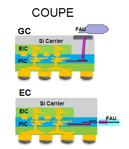
The AI era demands unprecedented optical bandwidth and energy efficiency. As electrical interconnects hit their limits, industry shifts towardCo-Packaged Optics (CPO)—bringing optical engines directly next to ASICs to minimize electrical losses.
TSMC is aggressively advancing silicon-photonics + advanced packaging, with theCompact Universal Photonic Engine (COUPE)serving as its flagship platform. COUPE uses SoIC 3D stacking to tightly integrate PICs and EICs with extremely low interconnect loss, supporting flexible coupling modalities and aiming for production windows around 2025–2026.
Metalenses align with several COUPE objectives:
Where Metalenses Fit into COUPE
Fiber/free-space coupling elements
Metalenses can reshape divergent waveguide output into a fiber-matched mode, improving coupling efficiency and reducing PDL and chromatic sensitivity.
Intra-module beam shaping
For vertical laser injection, detector illumination, or short-distance chip-to-chip free-space links, metalenses can focus or collimate beams in ultra-thin form factors.
Beam routing and steering
Metagrating-style metalenses can impart fixed deflection angles; future reconfigurable metalenses (phase-change, LC-over-meta) may support dynamic alignment or routing inside CPO modules.
Compensation and self-calibration
Metalenses with localized heaters or tunable materials can correct packaging-induced misalignment or drift.
Analysts have noted that TSMC is leveraging VisEra’s wafer-level optics (WLO) expertise to enhance CPO coupling—suggesting that metalenses are being actively evaluated.
Metalenses provide the “last-inch” optical control that COUPE needs in an ultra-compact 3D-IC-compatible package. As CPO architectures scale toward multi-Tb/s and multi-wavelength I/O, integrating metalenses into the optical engine will increasingly become a differentiating factor.
Manufacturing Challenges in Advanced Packaging Processes
Integrating metalenses into CPO (Co-Packaged Optics) modules introduces a series of manufacturing and process-integration challenges. CPO assembly typically involves wafer-level or die-level bonding—such as TSMC’s CoWoS 2.5D silicon interposer and the emerging SoIC 3D direct bonding technologies. These packaging steps often involve high-temperature compression, mechanical alignment, substrate-level interconnection, and other operations, each of which can pose risks to the delicate nanoscale structures already patterned on the chip surface.
First, if a metalens is placed on the surface of a photonic chip that needs to be direct-bonded to another die (such as a logic IC), that placement is clearly infeasible—the nanopillars would interfere with bonding or be crushed. Therefore, metalenses cannot reside on any interface that requires wafer-to-wafer bonding. For example, in TSMC’s COUPE architecture, the EIC (electronic IC) is stacked on top of the PIC (photonic IC). If vertical bonding (SoIC) is used, should the metalens be placed on the PIC’s top surface (adjacent to the EIC) or on its bottom surface (away from the EIC)? Since bonding requires a smooth, flat contact interface, a metalens clearly cannot occupy the bonding plane. A more reasonable arrangement is to place the EIC on top of the PIC via direct bonding, while placing the metalens on the PIC’s bottom optical-output surface—or alternatively patterning metalenses on the PIC’s top surface but leaving optical windows that allow vertically emitted light to exit.
In practice, COUPE currently emphasizes horizontal optical coupling (routing different bare dies through interposer RDLs). If no vertical emission is involved, metalenses could be placed at the PIC’s chip-edge output. For edge-coupled scenarios, one might consider fabricating metalenses on the vertical chip facet—by directly patterning nanostructures on the sidewall. However, such wafer-level sidewall nanofabrication is extremely challenging and is not yet a mature industrial process. A more realistic option is to fabricate metalenses on the PIC’s top surface and use vertical grating couplers or turning mirrors to redirect light toward the metalens, which then collimates the beam into a planar fiber-array interface.
Second, CPO packaging involves thermal processes that may limit the timing of metalens integration. In CoWoS, for example, a photonic engine (with integrated metalenses) may be mounted onto an organic substrate or silicon interposer and reflow-soldered. Reflow temperatures can reach ~260 °C, so the metalens material must withstand this temperature without shape distortion. Silicon and SiO₂ are stable at these temperatures, but polymer-based or phase-change metalenses require careful validation. Additionally, during assembly, mechanical pressure is applied—for example during underfill dispensing, molding, or chip attachment. Without protection, nanopillars could be damaged. Thus, after metalens fabrication, a transparent protective overcoat (e.g., SiO₂) or wafer-level cover glass may be required.
Third, alignment and positioning within the CPO module remain non-trivial. Although metalenses can expand alignment tolerances, the lens itself still must be accurately positioned relative to fibers or detectors. The focus point of the metalens must precisely coincide with the fiber core or photodiode. This requires high-precision lithographic alignment between the metalens and the underlying waveguides (tens of nanometers—achievable) and sufficiently tight positional tolerances during packaging. If the metalens has a short focal length, its depth of focus is shallow, meaning vertical placement errors during assembly must be tightly controlled. One mitigation is to intentionally design longer focal lengths or flat-top beam profiles to increase tolerance.
Finally, compatibility with CPO mass-production requires robust reliability validation. CPO modules in AI data centers must operate continuously for years with minimal maintenance. Metalenses must pass stringent tests—thermal cycling, high-temperature humidity, mechanical vibration, optical aging—ensuring nanoscale structures remain stable. In theory, metalenses are highly reliable (with no moving parts and stable materials like SiO₂/Si), but any shift in nano-geometry (e.g., contamination) can degrade performance and is not easily repairable. Thus, sealed, dust-free, and contamination-resistant packaging will be essential.
System-Level Value: How Metalenses Enhance CPO Modules
If these manufacturing challenges are solved, integrating metalenses into CPO brings system-level benefits:
- Smaller Packaging Volume
Traditional optical coupling requires volumetric lens assemblies and fiber-alignment fixtures. Metalenses eliminate these, enabling flat, on-chip optics. This reduces the overall footprint of CPO modules, enabling higher interconnect density or improved cooling—critical in AI systems with dozens or hundreds of optical channels per switch ASIC.
- Higher Coupling Efficiency → Lower Power
Reducing coupling loss by 1 dB lowers required laser power by 20–25%. If metalenses reduce link loss (e.g., from 2 dB → 1 dB), the transmitter power budget drops significantly. Scaled across hundreds of channels, the energy savings are substantial. TSMC has explicitly emphasized that improved photonic-electronic integration reduces copper interconnects and total system power. Metalenses contribute to this efficiency improvement.
- Higher Bandwidth Density
Metalenses alleviate optical limitations such as narrow grating bandwidth, polarization sensitivity, and chromatic dispersion. Through dispersion engineering and polarization control, metalenses can enable:
broader operating bandwidth
dual-polarization channels
improved DWDM signal quality
reduced PDL/PMD penalties
Given that COUPE targets >1.6 Tb/s per fiber, metalenses that maintain a common focal plane across 1550 ± 40 nm can significantly reduce ISI and improve link margins.
- Differentiated System Performance
In AI/HPC interconnects, even marginal efficiency or loss improvements translate into major competitive advantages. A 0.5 dB coupling improvement could allow customers to use lower-power lasers or extend link reach. For hyperscale data-center operators, such improvements compound into CAPEX and OPEX savings. If TSMC integrates metalenses into COUPE and secures patents around the approach, it gains a unique value proposition versus competitors.
Industry trends support this direction: reports indicate TSMC’s silicon-photonics patent filings overtook Intel in 2024, and analysts highlight VisEra’s emerging role in wafer-level optics for CPO. This suggests leading foundries now view metalenses as a critical component for enabling commercial CPO deployment.
- Process Matching & Manufacturing Yield: Metalens + Silicon Photonics Bottlenecks
Combining metalenses with silicon-photonics chips opens vast possibilities, but also reveals manufacturing bottlenecks. Silicon photonics relies on CMOS-grade maturity and yield, whereas metalenses introduce nanoscale patterning with new optical functions. Bridging the two requires overcoming several barriers.
This section analyzes process limits and yield-management issues and outlines what Taiwanese players such as VisEra, AuthenX, LDS, and Brillink must strengthen to meet mass-production demands.
- High-Aspect-Ratio Nanopillars and the Process Limits of Dense Metasurface Patterns
Nanofabrication Challenges
The functionality of a metalens comes from its densely packed nanoscale features—typically tens to hundreds of nanometers in diameter, with comparable pitch. Fabricating such fine structures requires advanced lithography and etching.
State-of-the-art immersion DUV (193 nm) or EUV tools, without multiple patterning, generally achieve40–50 nm resolution. For a 1550 nm metalens, nanopillar diameters are often100–300 nm, which is barely within DUV capability. However, the pitch may need to approachλ/(2NA); for NA = 0.8, the pitch can be <1 µm, and even smaller for precise phase control.
Electron-beam lithography (EBL) easily achieves the required resolution, but writing a full12-inch waferis extremely time-consuming and thus unsuitable for high-volume manufacturing (HVM). This creates a fundamental tension: although each metalens is small, using EBL for every chip would make productionprohibitively slow and expensive.
Nanoimprint Lithography (NIL) as a Solution

Source: ResarchGates
NIL provides a practical path:
A high-precisionmaster moldis fabricated once (via E-beam, grayscale lithography, etc.), then replicated across wafers through imprinting. NIL can reachsub-10 nm resolutionand replicate full-wafer nanoscale patterns quickly, making it attractive for mass production.
Challenges remain:
Mechanical pressure and resin fillingduring imprinting may stress pre-existing structures.
Overlay accuracymust reach optical-grade precision (tens of nanometers) to align the metalens with the underlying waveguide.
While such systems exist, integrating NIL into a silicon-photonics fab workflow requires coordination with foundries.
A plausible model:
Specialized optical manufacturers (e.g.,VisEra) develop NIL processes, and silicon-photonics fabs send completed wafers for metalens imprinting, which then return to the packaging line. This demands strong supply-chain cooperation, qualification, and tight quality control.
High Aspect Ratio and Deep Etching
To achieve sufficient phase delay, metalens nanopillars typically require heights ofseveral hundred nanometers to ~1 µmin the near-infrared. On silicon platforms, this implieshigh-aspect-ratio etching, which brings issues:
Sidewall taperingor roughness
ARDE (aspect-ratio-dependent etching)leading to non-uniform pillar height
Microloading effectsacross dense/isolated feature zones
While CMOS fabs have deep-trench expertise (e.g., DRIE), applying it uniformly acrosslarge-area nanoscale patternsremains an open challenge.
Possible mitigations:
Multi-step etchingto preserve pillar shape
ALD sidewall smoothingto reduce roughness
Optimizing etch chemistry for uniformity
But all of these increase process complexity.
Large-Area Yield Challenges
Even if metalens regions occupy only a small area on each die, thetotal nanopatterned area per wafercan be significant. For example, a 10 × 10 mm² chip with a 1 mm² metalens region, multiplied over an entire 12-inch wafer, results in a very large cumulative metasurface area.
This dramatically increases sensitivity to defect density.
Even a single particle per cm² falling on a critical metalens zone can drastically reduce coupling efficiency—or kill the channel entirely.
Unlike electronic circuits, optical metasurfaces offerno redundancy:
A damaged nanopillar produces a permanent hole in the phase profile that cannot be “repaired” by neighboring structures.
Therefore:
fabs needcleaner-than-CMOSenvironments
inspection equipment must detecttens-of-nanometers defects
Maintaining yield across such dense nano-patterns becomes one of the hardest challenges:how to monitor and control extremely small defects in a cost-effective, high-volume workflow.
Process Sequence, Material Impacts, and Reliability Considerations
Process-Flow Integration: Where to Insert Metalens Fabrication
Integrating metalens fabrication into a silicon-photonics process requires decidingwhich stageof the flow it should enter. Two general options exist:front-end integrationorback-end addition.
Front-End Integration
In this scenario, metalenses are patterned immediately after silicon-photonics waveguide fabrication, using the same wafer line and lithography tools.
Advantages:
Excellent alignment accuracy (waveguides and metalenses exposed on the same stepper).
No cross-fab wafer handling.
Challenges:
Material compatibility with subsequent CMOS steps:
If the metalens is silicon-based, later dielectric deposition and via/contact patterning may require surface planarization.
If the metalens uses SiO₂ nanopillars, high-temperature steps (e.g., annealing) might alter refractive index or cause material mixing.
Thermal & chemical exposure:
Metalenses would need to survive all remaining CMOS steps—temperatures above 400 °C, CMP, etchants, cleans—posing serious risk ofpattern erosion, deformation, or contamination.
Because of these constraints,front-end metalens integration is challenging, and today back-end approaches appear more feasible.
Back-End Addition
Back-end integration places the metalens processafterthe silicon-photonics wafer is fully fabricated and protected (typically with a planarized SiO₂ overcladding).
The wafer is then shipped to a specialized optical-fabrication line—such asVisErain Taiwan—for nanoscale patterning.
This approach avoids CMOS-line material restrictions and allows use of dedicated NIL/optical structuring equipment.
Key challenge:
Cross-fab alignment accuracy—ensuring every metalens aligns precisely with the waveguide emitter/receiver beneath.
Fortunately, modern wafer-fab coordinate systems and alignment marks can be used (e.g., retaining fiducials near waveguide regions), enabling accurate overlay.
Japan and Taiwan have already demonstrated wafer-level DOE mass production for 3D sensing devices. Since metalenses are fundamentally a type of DOE, the technology base is continuous.

A real precedent isUMC × Metalenz:
UMC fabricated metasurface layers using its 40 nm platform on 12-inch wafers and performed wafer-to-wafer bonding to sensors, achieving production-level quality. This validates thatback-end metalens processing with commercial yield is achievable.
Material Stress and Thermal Matching
Material selection is critical. Most silicon-photonics platforms use SiO₂ as an upper cladding. Patterning air holes (SWG) or depositing high-index nanopillars introducesCTE mismatchrisks.
During thermal cycling, mismatched CTE can accumulate micro-stress, eventually causingpillar loosening, tilt, or cracking.
Preferred materialsare those with CTE close to Si or SiO₂:
Si₃N₄ nanopillars (CTE close to SiO₂)
Polysilicon nanopillars (CTE close to crystalline Si)
GeSi for SWIR metasurfaces (CMOS-compatible, strong refractive index contrast)
Process constraints matter:
Polysilicon often requires ~700 °C LPCVD → unsuitable for back-end steps
Oxides via PECVD <300 °C → compatible
TiO₂ via ALD is low-temp but slow
Reliability also favorssingle-material, single-layermetasurfaces rather than multi-layer structures.
Role and Capabilities of Taiwanese Companies(VisEra,AuthenX,Brillink.ai,Latitude Design Systems (LDS))
Taiwan has a complete semiconductor and optoelectronics supply chain, but metalens-plus-silicon-photonics integration is cross-disciplinary and requires capabilities across IC manufacturing, optics, and nano-replication. Several Taiwanese companies are emerging in this domain:
A TSMC × Himax joint venture specializing in CIS packaging, color filters, and wafer-level optics. VisEra already develops nanoscale optical structures, including metasurface and nano-pillar processes.
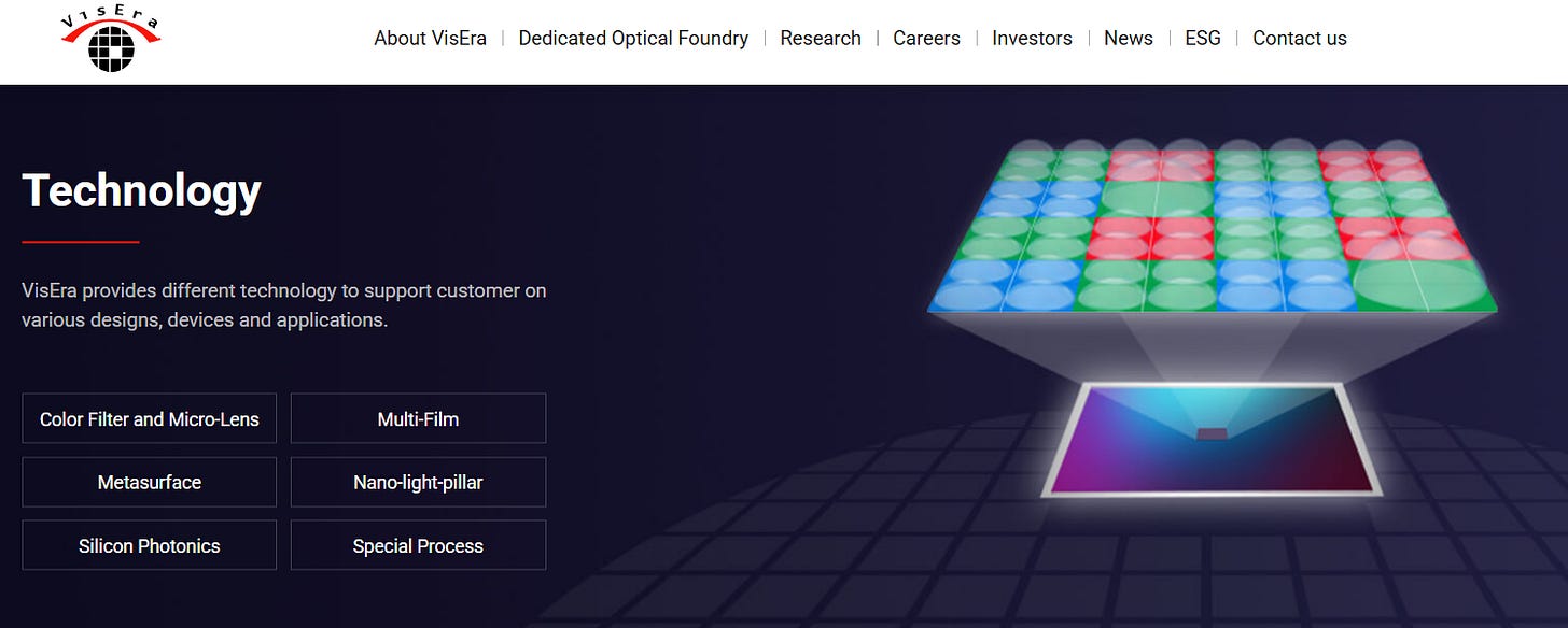
In 2025, VisEra and Artilux demonstratedCMOS-compatible metalenses on 12-inch waferswith high-volume manufacturing capability, proving commercial-grade yield for SWIR metasurfaces.
To enter silicon-photonics markets, VisEra will need to tune its processes for1550 nm operation, wafer layout requirements, and tighter alignment tolerances.
Backed by TSMC and positioned within the TSMC OIP ecosystem, VisEra may become a manufacturing hub for silicon-photonics metalenses.
A startup founded in 2019 specializing in optoelectronic solutions, with expertise in silicon photonics, lasers, and fiber-optics components.
AI-CPO (co-packaged optics for AI infrastructure) is highlighted as a target market.
AuthenX has showcased the use of metalenses inFAU (Fiber Array Unit)structures for CPO, enabling easier coupling to multi-core fibers. Demonstrations atSemicon Taiwan 2025confirm active engagement in the field.
To scale into major supply chains, AuthenX must further strengthen:
Automated optical metrology(focus, efficiency, uniformity)
Yield engineering
Module-level validation with large customers

Company Background & Mission
Brillink.ai is an optoelectronics startup founded in 2025 with the mission of “Bridging Brilliance to a Smarter Future”—leveraging light to connect human creativity with machine intelligence.
Its core team comes from the silicon photonics and semiconductor industries, with expertise spanning AI-driven design, Micro-LED, high-sensitivity photodetectors, and metalens-based optical packaging.
Key Products & Technologies
AI-Driven Silicon Photonics Design Platform
The company develops a scalable, AI-enabled silicon-photonics design platform that integrates PDKs and ADKs. Using generative AI, it automates design rules and layout generation, enabling customers to rapidly build high-speed optical modules.
Next-Generation Optical Interconnect Modules
Leveraging high-speed Micro-LEDs and high-sensitivity photodetectors from its parent company, Brillink.ai delivers short-reach optical-interconnect solutions offeringhigh bandwidth and ultra-low power consumption.
Advanced 2D Vertical Coupling with Metalens Integration
Brillink.ai uses photonic-crystal grating couplers and metalens structures to significantly shrink optical components, increase bandwidth density, and improve coupling efficiency.
This technology enablesvertical integration of emitters and photonic chips on a single wafer.
CMOS-Compatible Mass Production
All related processes support 12-inch CMOS manufacturing, facilitating cooperation with established semiconductor fabs for volume production.
Business Model & Services
The company offers:
High-accuracy PDK/ADK development
PIC design services
Micro-LED optical-interconnect module design & validation
Partnership models include co-development, contract development, and design-enablement engagements.
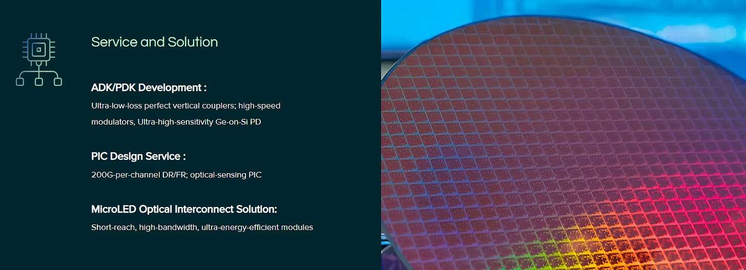
Position of Metalens in Brillink.ai’s Technology Stack
Brillink.ai uses photonic-crystal grating couplers combined withmetalensesto miniaturize optical components.
However, the company’s primary focus is on itsAI-driven silicon-photonics design platform and optical-module packaging.
Metalenses serve as one of the components for improving vertical-coupling efficiency—notas a product produced through large-scale laser direct structuring (LDS) or similar mass-fabrication methods.

Company Positioning:
Latitude Design Systems is a software company specializing inelectronic–photonic co-design automation (EPDA)tools. The slide deck was presented by Terence S.-Y. Chen in November 2025.
PIC Studio Integrated Platform
Their flagship product,PIC Studio, is an integrated EPDA solution that enablesfull co-simulation of optical transceivers, covering both electronic and photonic TX/RX models.
Its capabilities include:
Pre-layout and post-layout verification
High-frequency RLCK extraction and complex EM-thermal simulations
LVS/DRC verification
System-level simulation and auto-layout generation
TDECQ signal-quality analysis
Monte Carlo variation analysis
PIC Studio aims to unify the entire optical-electronic design workflow within a single environment.
Chip–Package Co-Design
The presentation highlights that today’s photonic EDA ecosystem still has significant gaps—such as limited automatic synthesis, weak testability methodologies, and insufficient support for curved-waveguide routing.
Latitude proposes aHolistic Co-Designmethodology:
Early integration ofPackaging Design Kits (PDKs)
Joint thermal, mechanical, and optical co-simulation between chips and packages
Risk reduction by linking chip-level design to packaging constraints from the beginning
This approach acknowledges that packaging is inseparable from modern silicon-photonics performance.
AI and Simulation Acceleration
LDS believes the future of photonic design will rely heavily on:
GPU-accelerated physical simulation
AI-based inverse design
AI-assisted verification and optimization
Their proposedEnd-to-End AI Design Agentsworkflow includes:
Specification interpretation
AI-driven circuit synthesis
Automated layout generation
Real-time simulation feedback
The goal is to reduce design cycles and push toward autonomous photonic-electronic co-design.
Foundry PDKs & Assembly Design Kits
Latitude advocates buildingunified electronic/photonic design kitsandextensible component models, along withPackaging-Aware PDKsthat consider:
Fiber-to-chip interface constraints
Thermal stress
Assembly tolerances
They further propose combining:
Assembly Design Kits (ADKs)
Thermal-coupled simulation
Extensible component libraries
Customizable auto-routing algorithms
This aims to close the long-standing gap between electronic and photonic EDA and enable truly integrated system design.
MetaStudio Tutorial: Automated Metasurface Design from Phase to Fabrication
MetaStudio is a comprehensive automation tool developed by Latitude Design Systems for designing metasurface optical components. The software streamlines the entire design workflow from phase distribution calculation to meta-atom optimization and final layout generation. It integrates advanced algorithms including particle swarm optimization, physical optics, Fourier optics, angular spectrum propagation, finite-difference time-domain (FDTD) methods, and rigorous coupled-wave analysis (RCWA) to ensure high-precision simulation and optimization tailored to engineering requirements.
What Taiwanese Companies Must Strengthen to Enter Metalens + Silicon Photonics Manufacturing

To penetrate the emerging metalens + silicon photonics supply chain, Taiwan’s manufacturers must reinforce the following capabilities:
- Mastering Mold Fabrication & Pattern Transfer
Develop high-reliability, large-area master fabrication (e-beam or multi-pattern DUV) and improve nanoimprint throughput and overlay precision.
VisEra has already made early moves in this direction, but further scaling of high-volume NIL and tooling infrastructure is needed.
- Wafer Bonding & Alignment
Achieve high-precision wafer-to-wafer and wafer-to-device bonding.
In metalens–photonics stacking or bonding to sensing ASICs,alignment accuracy and yield are both mission-critical.
Metalenz and UMC have demonstrated this with theirwafer-bonded polarization-sensing CMOS product, showing that the same approach can eventually be extended to bonding a standalone metalens wafer onto a silicon-photonics wafer.
- Inspection & Yield Management
Introduce advanced defect-inspection tools—potentially enhanced by AI vision—to detect subwavelength-scale pattern errors.
Next-generation AOI tools from Applied Materials, KLA, or similar vendors may become necessary.
At the same time, build statistical models linking metalens optical performance to process variations, forming a robust yield-prediction and control methodology.
- System-Level Optical Testing
Manufacturers must test not only structures but alsooptical performanceat wafer scale.
Examples include:
interferometric measurement of focal length and phase profile
miniature beam analyzers for wafer-level verification of efficiency and NA
Establishing such metrology is essential for guaranteeing product quality.
- Establishing a Design Ecosystem
Metalens design must be integrated into the broader silicon-photonics design flow.
This means collaboration with EDA vendors such asSynopsys, Lumerical, Ansys/LDSto support:
metalens modeling modules
co-simulation with electronic and photonic circuits
PDK-ready cell libraries for metasurfaces
AI-assisted design—e.g., deep-learning predictions of optical response or automated inverse-design—will further reduce entry barriers.
Matching Metalens Processes to Silicon Photonics Flows
Silicon-photonics processes are mature and stable; any new module must be introduced without disrupting the base flow.
Several strategies can enable compatibility:
Modular Process Insertion
Define the metalens module as an optional, off-line process step—similar to how TSMC handles InFO or CoWoS in packaging.
For example:
fabricate active photonic devices
transfer the wafer to VisEra for metalens processing
return to back-end packaging
As long as interfaces (bonding layers, alignment marks, contamination control) are standardized, this “upstream/downstream” model works smoothly.
OIP (Open Innovation Platform)–style interfaces could enable this.
Avoiding Interference with Electronics
Metalens fabrication must avoid conductive films or metallic residues that could affect CMOS reliability.
Ideally, the metalens is entirely dielectric.
Contamination and magnetic materials must also be avoided, particularly when processing above BEOL layers.
Thermal-Budget Control
Metalens processes must remain low-temperature.
If high-temperature steps are unavoidable (e.g., crystallization anneal), they must be extremely short or locally heated.
CMOS BEOL typically cannot exceed~400°C;300°C or loweris ideal.
This constraint may eliminate certain PCM-based tunable-metalens schemes, pushing adoption toward electrically or optically induced index-change mechanisms.
Standardization & PDK Integration
For true ecosystem integration, foundries must define aMetasurface Layerin their process stack—specifying:
minimum feature sizes
thickness constraints
validated optical models
Just as PDKs today include grating couplers or MMI cells, future PDKs may include standard metalens cells.
If TSMC collaborates deeply with VisEra, it could even providestandard metalens IP blocksfor fiber coupling, collimation, or beam shaping.
Wafer-Level Pre-Test & Post-Test
Silicon-photonics wafers undergo optical testing before dicing (e.g., grating-coupler efficiency maps).
Metalenses must be included in this process.
Dedicated test fixtures—array light sources aligned to metalens grids, efficiency monitoring, beam-profile extraction—will be needed.
In some cases, metalenses mightsimplifywafer-level testing by enabling direct vertical coupling into waveguides, removing the need for external lenses.
- Functional Expansion: Value-Added Use Cases of Metalenses in Silicon Photonics
Metalenses, as planar optical interfaces, can perform functions beyond simple focusing.
Their ability to manipulatephase, amplitude, polarization, and spectrumallows them to serve as programmable optical interfaces within silicon-photonics systems.
Below is a structured analysis of major functional categories:
Mode Matching & Mode Conversion
Metalenses can:
expand or collimate silicon-waveguide modes for free-space links
enlarge mode size for single-mode fiber coupling
act as multi-mode converters or mode filters
This reduces coupling loss and enables chip-to-chip free-space optical interconnects.
Beam Steering & Scanning
By applying phase gradients, metalenses can steer beams without moving parts—ideal for:
LiDAR
optical backplanes
reconfigurable interconnects
multi-core fiber routing
Dynamic metasurfaces using PCM, LC, or thermal tuning can enable beam scanning and switching.
Polarization & Dispersion Management
Metalenses can implement:
geometric-phase (Pancharatnam-Berry) polarization control
polarization splitting
group-delay compensation
broadband achromatic focusing across the full C+L telecom bands
This provides tools to solve inherent TE/TM asymmetry and chromatic-dispersion problems in silicon photonics.
Reconfigurable & Tunable Functions
Tunable metalenses enable:
adaptive focusing
optical alignment correction
on-chip optical switching
optical beam routing
dynamic modulation (if integrated with EO elements)
This unlocks new architectures in data-center switching, AR/VR, sensing, and free-space optical links.
- Industry Chain & Business Models: Positioning Metalenses in Silicon-Photonics Manufacturing
With the technical foundations established, the next step is industrialization—coordinating R&D, supply-chain roles, commercial models, and market strategy.
In the following section (if needed), I can elaborate on:
division of labor among design firms, mold/tooling vendors, foundries, and system companies
licensing/IP models
potential winners in Taiwan’s ecosystem
market-size projections and competitive positioning
From Research Validation to Mass Production: Becoming Part of the Wafer-Level Optics Manufacturing Flow
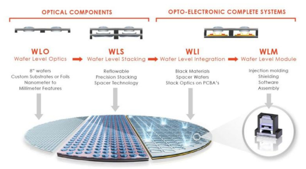
Metalenses first appeared mainly in academic research and small-scale prototypes. But how can they reach the maturity required for mass production? The key is integrating them intowafer-level optical (WLO)manufacturing. In recent years, WLO has gained traction—for example, smartphone camera modules already use wafer-level lenses. The integration of metalenses with silicon photonics can be viewed as WLO extending into the optical-communications domain: implementing optical functionality through wafer processes rather than assembling discrete components.
To become part of the wafer-level flow, several conditions must be met:
- Mature and Stable Manufacturing Processes
This means metalens fabrication must reach CMOS-level stability, with minimal batch-to-batch variation, allowing continuous production once the equipment is calibrated.
There are signs that this is already happening in some applications. For example, theMetalenz–UMC PolarID polarization-sensing solutionhas successfully entered mass production and passed supply-chain qualification. Their announcements emphasize that supply-chain certification and 12-inch wafer-fab capability accelerated volume readiness for OEMs.
This demonstrates thatonce a major foundry commits, metalens technology can indeed complete the full path from R&D to qualification and production.
- Standards and Specifications
For widespread industry adoption, standardization is essential. This includes standardized definitions for metalens optical performance—such as efficiency, bandwidth, and loss—as well as uniform test methodologies.
In optical communications, standards bodies likeIEEEandITUalready define interface and component requirements. If metalenses become widely used, it is likely that new standards will emerge to define classes, interoperability, and performance levels for metalens-based optical couplers.
- Successful Pilot Products
New technologies often need one or two commercial successes to build market confidence. In the metalens + silicon-photonics space,PolarIDis already a proven example in the biometric-sensing domain.
For high-speed optical communications, we may soon see announcements such as:
“An AI switch now adopts a silicon-photonics transceiver with metalens coupling.”
Once a major vendor demonstrates clear advantages—size, coupling efficiency, cost, thermal stability—the rest of the industry will quickly follow.
TSMC’s COUPE platform, if launched in 2026 with claims that metalenses are integrated to enhance performance, would be amajor catalyst for the entire sector. A public endorsement from TSMC signals that metalenses are both feasible and economically justified. Other foundries and optics suppliers would rapidly adopt similar processes to avoid falling behind.
Ecosystem and Collaboration Models
Metalens + silicon photonics spans both optical and electronic domains—no single company can independently handle the entire chain from design to manufacturing and packaging. A healthy ecosystem is therefore essential. Several collaboration models may emerge:
- Design Company ↔ Foundry Collaboration
Specialized metasurface design companies create metalens structures and provide GDS files to wafer foundries for production.
Metalenz (a U.S. startup) is a classic example: it does not own a fab, but partners with UMC, ST, and others to license its designs for mass manufacturing.
A similar model could appear in silicon photonics: dedicated meta-optics IP vendors providing metalens IP cores for various applications. Foundries would then incorporate these into their process flows, similar to semiconductor IP licensing.
- Mold / Equipment Supplier ↔ Foundry Partnership
Some companies may focus on supplying nanoimprint molds or customized lithography tools to help foundries develop metalens capacity.
Examples include:
Large-area e-beam writing for hard materials (outsourced to specialized vendors, then used by foundries for NIL mass production)
Metrology companies developing inspection tools optimized for metalenses to improve yield
This type of supply-chain collaboration follows atechnology-providermodel.
- Vertical Integration
Large companies such as TSMC may prefer full control over the entire process, including design.
If TSMC builds an internal metasurface-design team and combines it with VisEra’s manufacturing capabilities, it could offer an end-to-end service model:
The customer specifies the required coupling or lens function, and TSMC handles design, simulation, fabrication, and final delivery of a chip with an integrated metalens.
This aligns with TSMC’s longstanding ecosystem strategy (end-to-end integration). In fact, TSMC’s R&D teams are already exploring metasurface research, including topology optimization. It is plausible that TSMC may eventually release an official metalens PDK component or design service.
- Joint Development with End Users
Major downstream players—such as hyperscale datacenter operators or cloud service companies—may co-invest in metalens + silicon-photonics development tailored to their needs.
NVIDIA’s co-development with TSMC for CPO is a prime example.
If NVIDIA wants to improve optical-module performance, it could easily fund metalens R&D executed by TSMC, with exclusive access to the results for a period of time.
This accelerates technology convergence because end-market requirements and funding are both clear.
Metalens Commercialization Requires a Clear, Collaborative Value Chain
The Taiwanese companies mentioned earlier may already represent an emerging model.
For example:

Artilux (design + system application) + VisEra (manufacturing) + TSMC ecosystem (integration & packaging)
successfully developed GeSi metalens devices.
In optical communications, we may eventually see combinations like:
AuthenX (design & application) + VisEra or UMC (manufacturing) + system vendors / networking OEMs (application validation)
working together to build CPO modules.
Such collaboration inevitably involves negotiation over business models:
IP owners(design companies): license fees or per-wafer royalties
Manufacturers: wafer-processing fees
Packaging/system vendors: system value capture (module or service revenue)
If a fully integrated player like TSMC handles everything, the model becomes:
Foundry fee + value-added service fee.
Because metalenses create significant added value, every part of the supply chain seeks to hold key positions to maximize profits. Therefore, commercialization must be built onclear division of responsibilities and mutual trustacross the ecosystem.
Commercialization Barriers and How to Address Them
To bring metalens + silicon photonics into true commercial deployment, several practical, non-technical barriers must be overcome in addition to the core technology itself:
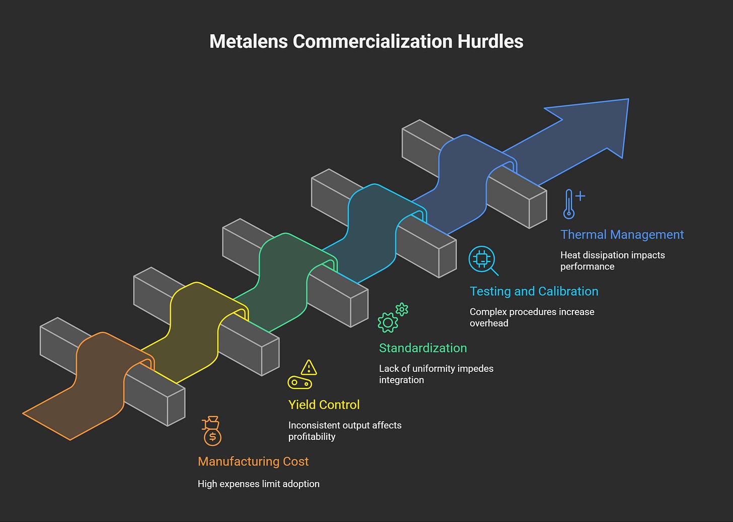
- Manufacturing Cost
Adding metalens fabrication steps increases overall processing cost. If these steps are too expensive or time-consuming, customers may be reluctant to adopt the technology. Cost reduction must come from process innovations—such as using high-volume NIL to reduce per-wafer writing cost, or improving yield to reduce scrap.
A positive example is Metalenz’s claim that its meta-optic camera technology canreduce camera-module cost, because one metalens can replace several curved lenses and can be fabricated at wafer scale.
In optical communications, if metalenses can replace costly alignment steps or increase module throughput, customers will be willing to accept additional wafer-processing cost.
- Yield Control
As mentioned previously, large-area metasurface patterns can reduce overall yield. If metalens failures cause some dies on the wafer to be scrapped, the total yield drops and cost rises. Yield-management strategies are therefore critical.
Possible approaches include:
Local redundancy:Fabricate two metalens structures on each die; use only one. If inspection shows defects in structure A, switch to structure B—similar to redundancy in electronics.
System-level tolerance:Allow certain optical channels to have slightly lower performance (with optical-power margins), preventing full die scrap.
Enhanced in-line inspection:Identify problematic wafers early and adjust process parameters to maximize final yield.
- Standardization
Metalenses are still a new technology, and parameters vary widely across vendors, making system companies hesitant. Industry-wide standardization would help—e.g.:
defining the equivalent performance of a metalens coupler (“equivalent to an x-µm length of SMF, y-dB insertion loss, Telcordia-compliant”)
specifying test conditions and reliability criteria
standardizing optical models and including metalens elements in commercial simulation libraries
If designers can drag-and-drop a verified metalens element into their simulation flow—just like a grating coupler—adoption will accelerate dramatically.
Well-known journals and organizations have already begun publishing metasurface reviews and roadmaps, discussing manufacturing and application challenges. This is effectively laying the groundwork for industrialization.
- Testing and Calibration
Large-scale adoption of metalenses may complicate testing. Each module may require verification that the metalens coupling efficiency meets specification; otherwise, the optical link may have latent issues. This adds calibration steps and increases cost.
Manufacturers may need to integrate dedicated test structures near the metalens to enable rapid inspection. Developing automated, high-throughput testing methods will be a major priority for production engineers—ensuring that metalenses do not become a bottleneck in mass production.
- Thermal Management and Reliability
Silicon-photonics modules often operate near high-power lasers, where temperatures rise. Important questions include:
Does the temperature-dependent refractive index (thermo-optic coefficient) degrade metalens performance?
Do nanostructures deform after long-term high-temperature stress (e.g., 85°C aging tests)?
Can metalenses withstand rapid temperature/humidity cycling in outdoor equipment such as 5G fronthaul modules?
If metallic layers are used in the metasurface, how is oxidation prevented?
Most CPO applications run in relatively mild datacenter environments, but reliability must still meettelecom-gradeexpectations (decades-long lifetimes). The supply chain may therefore need a dedicated reliability-qualification framework—temperature cycling, vibration, drop tests, optical-power aging, etc.—to verify metalens module durability.
The earlier such reliability data is built, the faster customer concerns can be addressed.
Future Opportunities: Differentiation Advantages Under Massive Market Potential
Despite the challenges, the upside of successfully integrating metalenses with silicon photonics is enormous. Over the next 5–10 years, AI, 5G/6G, autonomous vehicles, and IoT are all expected to drive explosive growth in optical communication and sensing markets.
AI Data Centers
Industry forecasts show that optical-interconnect demand inside AI clusters will surge dramatically. InfiniBand switch bandwidth per port is expected to rise from800 Gbps → 1.6 Tbps → 3.2 Tbps, and eventually12.8 Tbps.
Silicon photonics is the enabling technology for these rates. If metalenses can be successfully integrated, they effectively give silicon photonics a“turbocharger”, enabling higher bandwidth at lower power.
Given the massive scale of future data centers, TrendForce reports that silicon photonics willreshape the cloud industry. If metalenses become a core part of this optical stack, their market value may rival that of any mainstream optical component.
High-Performance Computing (HPC)
Supercomputers demand extreme optical-interconnect performance—every0.1 dB loss reductioncan save several kilowatts of power. Metalens-enhanced silicon-photonic modules could stand out in HPC environments.
In emerging architectures such aschip-to-chip optical buses, free-space interconnect enabled by metalenses would be particularly attractive.
5G/6G Fronthaul and Communications
While today’s 5G backhaul relies heavily on fiber, future 6G may require dynamic, reconfigurable optical-access networks—an opportunity formetalens-based optical switches.In addition, adaptive metalenses may enableenvironment-aware communication/sensing fusion, such as smart lampposts equipped with optical-antenna arrays for V2X connectivity and ranging. These represent promising new markets.
Sensing and Imaging
Metalenses have already shown strong potential in3D sensing, facial recognition, and VR/AR displays.
If combined with silicon photonics—e.g., silicon-photonic projectors paired with metalens imaging in AR glasses—they may enable entirely new device architectures.
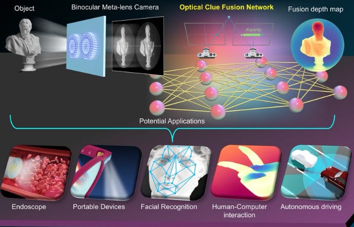
Market studies project the global metalens market to grow from$41.8M in 2024 → $2.4B in 2031, aCAGR of nearly 80%.
With such explosive growth ahead, Taiwan cannot afford to be absent from this field.
The TSMC COUPE Example: A Strategic Inflection Point
TSMC’s investment in silicon photonics and advanced packaging aims to secure a central role in the AI/HPC era. Metalenses are well positioned to enhance COUPE’s competitiveness.
According to Fudzilla, TSMC is using COUPE to tightly integrate photonic and electronic dies, leveraging VisEra’s wafer-level-optics capability and incorporating metalenses to improve coupling efficiency—presented as a key selling point to customers.
Intel has historically led in silicon photonics, but TSMC’s innovations may allow it toovertake Intel after 2025.
This illustrates a broader truth:whoever first matures metalens + silicon photonics integration may lead the next generation of optical-electronics markets.
Conclusion: Metalens + Silicon Photonics Is Optics Entering the “Moore’s Law Fast Lane”
The fusion of metalenses with silicon photonics effectively brings optics into the world of Moore’s-Law scaling.
It transforms what used to be discrete, alignment-heavy optical components into wafer-fabricated structures—bringing revolutionary gains in volume, performance, and cost.
Challenges remain—manufacturing yield, standardization, reliability qualification—but recent industry developments show strong momentum and early commercial success.
Once the technology stabilizes, metalenses will no longer be exotic laboratory devices; they will become astandard building blockof silicon-photonics chips.
In future AI data centers, high-speed communication networks, and advanced sensing systems, we can expect to see“Taiwan-made wafer-level metasurface lenses”playing a vital role.
As mass production accelerates, the global optoelectronics industry is poised for a new wave of growth—one filled with extraordinary potential.
Finally, let’s address the question many people have been asking: What exactly is Himax’s strategy in metalens?

But when we examine its production footprint in Tainan and Minnesota, its nanoimprint and 3D mold capabilities, the actual responsibilities of its optical engineers, and supply-chain signals surrounding TSMC COUPE and AR/3D sensing applications, a clear picture emerges:
Himax already treats metalens/metasurface optics as the next evolutionary step of its WLO business.
It functions as themeta-optics/matalens mold center, mass-production platform, and system-integration partner—rather than a company launching a consumer-facing “Metalens product.”
Himax’s technical foundation is built on top of its WLO business
Its ecosystem hinges on two strategic hubs:
- Himax Advanced Optronics Center, Tainan Tree Valley (Taiwan HQ)

Located near the Southern Taiwan Science Park, this campus operates two large-scale glass/polymer WLO production lines with an output of~34,000 8-inch-equivalent optical wafers per month.
These lines manufacture high-volume optics for 3D sensing and smartphones:
DOEs for structured-light / ToF dot projectors
Microlens arrays for collimation and pattern shaping
Multi-layer WLO lenses (2–3 layer stacks) showcased at CES
Reflow-compatible micro-optics for 3D sensing and AR/VR modules
Himax publicly states that this WLO engine has shipped:
500+ milliondiffractive optical elements for 3D recognition
50+ millionsmartphone lenses
100,000+waveguide AR glasses
This demonstrates over a decade of operating experience inhigh-volume, microstructured optics—with mature yield, cost structure, and customer relationships.
- Himax IGI Precision, Minnesota (USA)
Acquired in 2018, IGI forms thefront-end tooling centerof Himax’s meta-optics capability.
It provides the complete3D nano-patterning pipeline:
Photoresist master fabrication
Grayscale masks
E-beam / laser direct writing
Nickel electroforming shims
Soft molds
Support for NIL, injection molding, roll-to-roll, embossing
IGI highlights its ability to handlemicrostructure and nanostructure patterns, targeting 3D sensing, automotive LiDAR, micro-LEDs, and waveguide optics.
From a process-integration viewpoint,“Tainan WLO mass-production” + “Minnesota IGI nano-pattern tooling”is effectively a complete end-to-end meta-optics manufacturing pipeline. The outward branding still emphasizes DOE/MLA/waveguide optics, but in essence, this is the foundation of a futureMetalens foundry.
Optical perspective: metalenses are the natural extension of DOE/WLO
A metalens is essentially anextreme version of a DOE/metasurface—with subwavelength pitch and fully programmable phase profiles.
Himax’s current WLO stack already covers:
refractive microlenses
general DOEs
advanced beam shaping
waveguide coupling structures
Moving toward metalens is therefore acontinuation, not a restart.
Metalens fabrication typically involves:
E-beam / grayscale lithography / direct-laser writing for a high-resolution master
Nickel electroforming to create production shims
NIL / injection molding replication onto glass or polymer wafers
Thin-film deposition and etching for final structures
This maps almost perfectly onto theIGI + WLOcapabilities Himax already publicly lists.
IGI provides the high-resolution 3D masters and shims; Tainan WLO performs wafer-level imprinting/molding at scale. The34,000 wafers/monthcapacity is exceptionally large for meta-optics.
Thus:
Metalens at Himax is not a “zero-to-one” new line—it is a natural extension built directly on top of the existing DOE/MLA WLO platform.
Once the design libraries and materials mature, the mass-production infrastructure is already in place.
A more direct set of clues pointing to metalenses comes fromthree dimensions: patents, talent signals, and capital-market / supply-chain commentary.
From apatentperspective, although there is an entire patent family titled “Structured light projector including an integrated metalens and diffractive optical element,” later patents related to 3D structured-light projection cite this metalens-projector patent as prior art—specifically in Himax Technologies Limited’s dot-pattern projector filings. This indicates that when Himax designs its own structured-light architecture, it indeed treats metalens/metasurface elements as part of its usable design space, rather than an “academic buzzword” to be ignored.
Thetalentevidence is even more explicit: on LinkedIn, one can find the resumes of Himax optical engineers listing work not only on Diffractive Optical Elements (DOE) for 3D sensing and Computer-Generated Holograms (CGH) for AR-HUD, but explicitly“Metalens (Metasurface) design.”This confirms that Himax already has internal teams performing real metalens/metasurface design work—though these designs may ship under names such as “dot projector module,” “waveguide in-coupler,” or “customer-specific 3D sensing optics,” rather than any public-facing “Himax Metalens™” brand.
Thecapital-market and supply-chainsignals provide another angle: analysts and industry observers commenting on the TSMC COUPE supply chain have noted—“Metalens yield has improved significantly, the company has entered production, and customers are starting small-scale adoption… Himax will only handle Gen 1–2; later generations will be transferred to TSMC’s subsidiary VisEra ”
This aligns with analyst reports you have seen stating “Himax exclusively supplies the microlens arrays for COUPE Gen 1 and Gen 2.” Together, these point to a coherent narrative:
In thefirst two generationsof COUPE, the required high-precision microlens / optical structures are supported by outside WLO experts such as Himax, helping TSMC bring up the line and debug early generations.
As metalens yield and stability improve,later generations of the COUPE optical engine may gradually shift to metasurface/metalens architectures, and once mature, migrate into TSMC’s internal OSAT ecosystem (VisEra) to achieve large-scale, deeply integrated manufacturing.
For Himax, this positions the company as the“ignition engine”of the new optical platform: capturing high-margin, high-complexity NPI orders in the 0→1 phase, then redeploying accumulated metalens/meta-optics know-how into larger-volume markets such as mobile 3D sensing, AR/VR waveguides, automotive LiDAR, and more.
Three Application Battlegrounds for Himax’s Metalens Strategy
Across application and customer dimensions, Himax’s metalens presence can be divided intothree real, commercial deployment tracks:
- 3D Sensing & Mobile / Device Structured Light
This is Himax’s core WLO business—structured light, ToF, LiDAR, DOE + MLA + collimators—with hundreds of millions of units already shipped to smartphone and 3D-sensing customers.
In this domain, metalens value comes from replacing traditional collimators or pre-shapers with asingle metasurface, enabling:
reduced optical module thickness (lower z-height)
complex wavefront shaping (batwing profiles, random scattering, polarization-selective patterns)
reduced speckle
fewer stacked DOEs
and even direct metalens+DOE integration on theVCSEL emission surfacefor chip-scale projection heads
Here, Himax acts asdesign + mold + mass-production ODM/foundry, while system architecture is controlled by mobile and 3D-sensing OEMs.
- AR/VR/MR Optical Systems
Himax has bothLCoS microdisplays(HX70xx / HX73xx) andWLO waveguide couplerexperience, and has showcased multi-layer lenses, DOEs, MLAs, and waveguide optics at CES—making it an ideal “one-stop vendor” for all micro-optics within AR glasses.
Metalenses/metasurfaces can serve as:
waveguide in-couplers / out-couplers
collimation optics
polarization-selective metalenses
thickness-reducing components
FOV and distortion-management elements
This positions Himax strongly for near-eye optics as AR devices scale.
- Automotive LiDAR, In-Cabin Sensing, Industrial & Medical Optics
Himax’s official application pages already list DOE/WLO deployments in automotive LiDAR, in-cabin sensing, and 3D sensing, with cumulative shipments in the hundreds of millions.
Metalenses can play roles such as:
beam shaping for LiDAR (custom FOV, dot patterns)
in-cabin dot projection
ultra-miniature endoscope / biosensing optical heads
compact industrial sensing modules
In the broaderCPO/OIO ecosystem, these remain “edge sensing” applications—but once metalens technology matures, Himax’s WLO line can become ameta-optics contract manufacturing hubfor mobile, automotive, AR devices, and datacenter-peripheral optical modules.
Overall Conclusion: Himax’s True Role in the Metalens Ecosystem
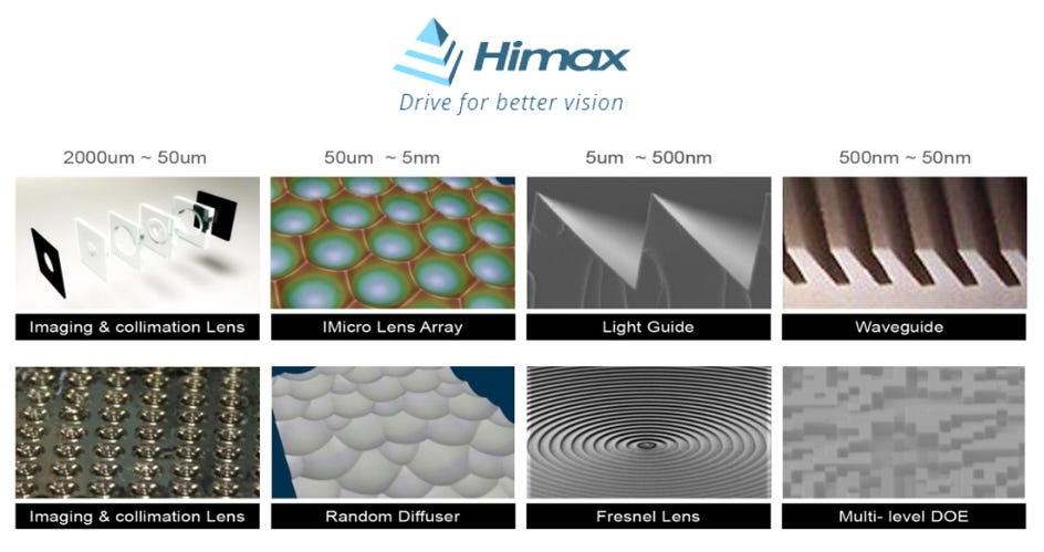
Himax does not publicly market a “Metalens™” brand, but in practice:
the Tainan WLO glass/polymer wafer-level optics line
combined with Minnesota IGI’s grayscale/e-beam/direct-write → NIL master → electroformed shim → imprint / injection / R2R pipeline
already forms afull manufacturing stack ready for meta-optics and metalens production.
Internal engineers listing “Metalens (Metasurface) design,” patent citations referencing metalens projectors, and COUPE supply-chain commentary (Himax handling Gen 1–2 microlenses, later generations shifting to VisEra) all point to the same conclusion:
Himax is simultaneously:
The launch supplierfor early-generation COUPE microlens / meta-optics.
A key fabrication & mold-platform providerfor future AR / 3D-sensing metalens modules.
If we articulate the future industry division of labor explicitly:
System/platform companies(Google, Apple, TSMC, major automakers) define system architecture.
Meta-optics design houses(Metalenz and others) provide layout & IP.
WLO/NIL specialists like Himax/IGIturn these designs intomass-producible, testable, packageable physical components, reusing the same process + mold infrastructure across mobile, AR, automotive, and optical-I/O modules.
This is thereal strategic positionof Himax within the metalens ecosystem.
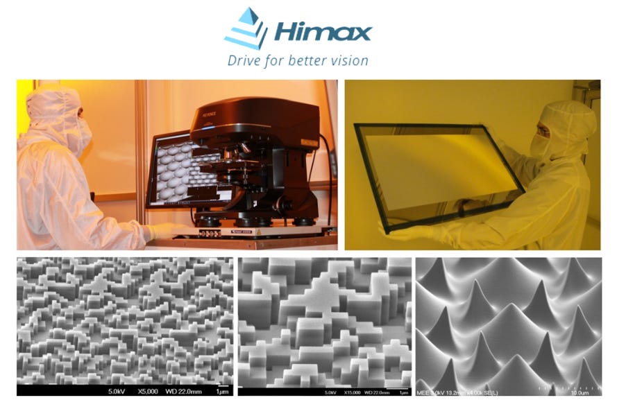


PreviousNext
TopLatestDiscussions








See all