The Next Frontier of AI in Consumer Tech: AR Glasses
The Next Frontier of AI in Consumer Tech: AR Glasses
- Source: SemiVision
- Author: SEMIVISION
- Published: 2025-11-06T21:20:30+08:00
- URL: https://tspasemiconductor.substack.com/p/the-next-frontier-of-ai-in-consumer The Next Frontier of AI in Consumer Tech: AR Glasses


The Next Frontier of AI in Consumer Tech: AR Glasses
Original Article by SemiVision Research (PIC Summit Europe, Meta,Applied Materials, Microsoft)

Nov 06, 2025
∙ Paid

At the2025 North America Technology Symposium, TSMC underscored its expanding role beyond traditional semiconductor applications by highlighting two transformative growth areas:augmented reality (AR)androbotics. Both fields represent not only the next frontier of consumer and industrial technology, but also a new wave of demand for cutting-edge chips that enable intelligence, connectivity, and real-time interaction.

2025年4月24日
Among these, AR glasses stand out as one of the most promising AI-driven products to enter everyday life. Unlike smartphones or laptops, AR glasses aim to seamlessly blend the digital and physical worlds, delivering contextual information, real-time translation, navigation, and AI assistance — all directly within a user’s line of sight. Achieving this vision requires breakthroughs indisplay technology, image processing, connectivity, and power efficiency— areas where TSMC’s advanced nodes and packaging technologies will play a decisive role.

2025年4月25日
Why glasses is the most suitable carriers for AI?
Among various smart devices, glasses have become one of the most suitable carriers for AI large models. As a traditional and widely adopted wearable device, glasses hold enormous potential for intelligent transformation.
The form factor of glasses places them close to the ears, eyes, and mouth—three of the body’s most important sensory organs—making them a natural, intuitive, and always-available interface for interaction with multimodal AI. With AI-powered smart glasses, users can listen to music, chat with an embedded large model, capture photos or short videos, and even share what they see directly with the model. At the same time, the model can use the built-in cameras to perceive the surrounding environment, enabling image recognition and other forms of visual processing for more comprehensive information handling.
In addition, the AR display capabilities of smart glasses provide AI with a powerful output channel for text and images, allowing users to receive information in richer, more immersive formats. For these reasons, the potential of AI-empowered smart glasses deserves close attention.
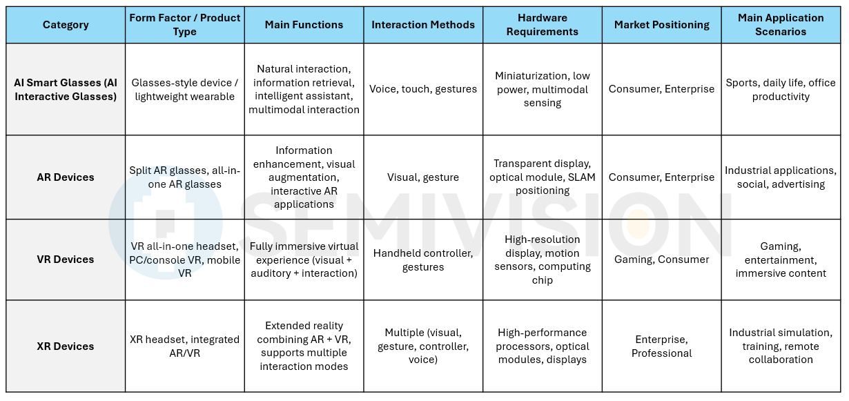
With the rapid rise of AI technologies, a wave of new startups and established brands have begun targeting the AI smart glasses segment. Compared with traditional XR devices, AI smart glasses integrate AI capabilities while focusing mainly on vision and hearing functions. This eliminates the need for the bulky optical systems typical of XR products, making AI glasses lighter, more comfortable to wear, and better suited for daily-life scenarios. Their reduced “device boundaries” enable more natural use, allowing users to seamlessly capture images, livestream from a first-person perspective, listen to music, make calls, and engage in real-time AI voice interactions.
As AI development increasingly shifts toward edge and consumer endpoints, AI smart glasses are emerging as a promising new platform for real-world AI applications. By combining visual, auditory, and language-based interactions—the most important sensory channels for humans—AI glasses are well-positioned to become a next-generation interface for AI adoption.
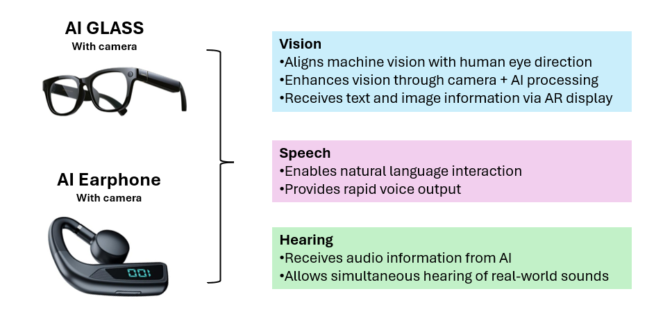
Here at SemiVision, we dare to make a bold prediction: while AI glasses are currently attracting the most attention as the natural carrier for multimodal AI, they may not be the only—or even the ultimate—form factor. Not everyone enjoys wearing glasses, whether for comfort, style, or practicality. For these users, an AI earphone in an ear-hook design could emerge as a powerful alternative.
Unlike conventional earphones, this new generation of AI-powered ear devices is expected to integrate a built-in camera, microphone array, and intelligent processing capabilities, enabling it to deliver the same core functions as AI glasses: computer vision, real-time multimodal interaction, and AR-like information feedback (via audio instead of visual overlay). In essence, the AI earphone could offer vision, speech, and hearing functions within a more discreet, lightweight, and socially acceptable form factor.
If this trend materializes, we may see two parallel hardware ecosystems evolve: one led by AI glasses with AR displays for immersive experiences, and another led by AI earphones for users who value simplicity and comfort. SemiVision believes that the winner may not be decided by technology alone, but by user adoption and lifestyle integration—and in that race, the AI earphone has the potential to become the “dark horse” of the multimodal AI era.
Roadmap of Near-Eye Display Development
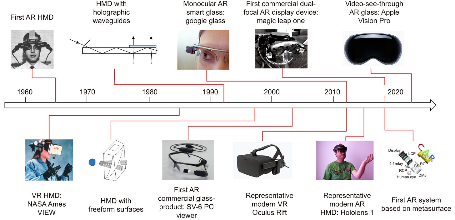
The history of near-eye displays, including both virtual reality (VR) and augmented reality (AR) head-mounted displays (HMDs), spans more than half a century. Over this time, technology has advanced from bulky prototypes to lightweight, highly integrated smart glasses and mixed-reality systems. The roadmap highlights several key milestones that have shaped the evolution of near-eye displays.
The First AR HMD Prototype (1968)
The story begins in 1968, when computer scientist Ivan Sutherland developed the first head-mounted display prototype, often called the “Sword of Damocles” because of its size and ceiling-mounted suspension. Although primitive, it demonstrated the concept of overlaying computer graphics onto the user’s view of the real world. This system laid the foundation for AR research and established the vision of blending virtual content with physical reality.
NASA Ames VR HMD (1970s–1980s)
During the following decades, government and aerospace research labs took interest in immersive displays. At NASA Ames Research Center, the VIEW VR HMD was developed to support space exploration training and simulation. It represented one of the earliest applications of head-mounted displays for practical, mission-oriented use, showing how immersive technology could enhance human performance in extreme environments.
Advances in Optical Design: Waveguides and Freeform Surfaces (1990s)
In the 1990s, researchers began experimenting with optical waveguides and freeform surfaces for near-eye displays. These approaches were aimed at reducing bulk, improving field-of-view, and delivering more natural visual experiences. Waveguide-based devices allowed images to be coupled into thin transparent substrates, while freeform optics provided novel ways of bending and shaping light paths. These advances would later become the backbone of modern AR displays.
The First AR Commercial Glass Product: SV-6 PC Viewer (2003)
The early 2000s saw the first attempt to commercialize AR glasses. In 2003, MicroOptical introduced the SV-6 PC viewer, a monocular see-through display that could connect to a personal computer. Although limited in resolution and functionality, it marked the transition from research prototypes to consumer-oriented products. The SV-6 highlighted both the promise and the challenges of wearable AR, particularly regarding ergonomics and cost.
Monocular AR Smart Glass: Google Glass (2012)
Modern VR and AR HMDs (2010s)
The mid-2010s witnessed rapid advances in both VR and AR systems. Oculus Rift, released in 2012, became a representative modern VR headset. Its high-quality tracking and immersive display helped kickstart the consumer VR industry. On the AR side, Microsoft introduced HoloLens 1 in 2015, which used optical waveguides to project holographic images directly into the user’s view. This represented a leap forward in both optical design and system integration, setting the stage for enterprise AR applications.
Dual-Focal AR Displays: Magic Leap One (2018)
In 2018, Magic Leap released Magic Leap One, the first commercial AR headset with a dual-focal display system. By supporting multiple focal planes, it attempted to address the vergence-accommodation conflict, a major visual comfort issue in AR displays. Although adoption was limited, the device demonstrated innovative optical approaches and highlighted the importance of solving human-vision-related challenges in AR.
AR Systems Based on Metasurfaces (2018)
Also in 2018, Lee and colleagues proposed the first AR system based on metasurface optics. Metasurfaces—ultrathin, nanostructured films that manipulate light at sub-wavelength scales—offered the potential for compact, lightweight, and highly functional AR optics. This work showed a new research direction that may enable future breakthroughs in near-eye display miniaturization.
Video-See-Through AR Glass: Apple Vision Pro (2023)
Most recently, Apple introduced the Vision Pro in 2023, a video-see-through AR headset. Unlike optical see-through designs, the Vision Pro uses high-resolution cameras to capture the outside world, which is then digitally combined with virtual content and displayed to the user. This approach provides flexibility in rendering and seamless integration of digital and real environments, though it raises challenges such as latency and power consumption. Apple’s entry has reinvigorated the industry and signaled growing consumer demand for immersive AR experiences.
2025年9月4日
Meta Ray-Ban Display and Meta Neural Band
At Meta Connect, Mark Zuckerberg unveiled theMeta Ray-Ban Display, the company’s most advanced pair of AI glasses to date, paired with a groundbreakingMeta Neural Band. Together, these products mark the next evolution of wearable AI technology.
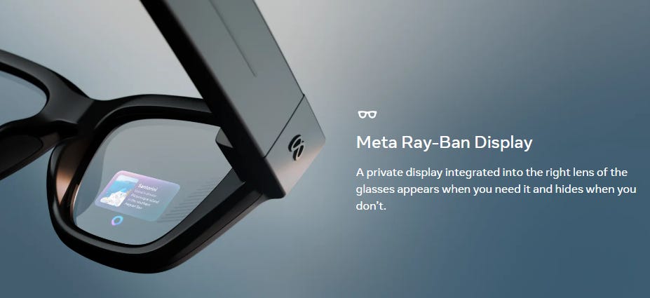
TheMeta Ray-Ban Displayintroduces afull-color, high-resolution in-lens displaydesigned to be both useful and unobtrusive. With a quick glance, users can check messages, preview photos, access translations, or get assistance from Meta AI — all while staying engaged with the world around them. The display isn’t always on; instead, it appears only when needed, ensuring that the glasses complement your daily flow rather than dominate your attention. Unlike bulky headsets, these glasses remainlightweight, stylish, and comfortable, blending seamlessly into everyday life.
Complementing the glasses is theMeta Neural Band, anEMG wristbandthat interprets tiny muscle signals in the wrist and fingers. This enables users to control their glasses with subtle gestures — swipes, pinches, or even micro-movements — without needing to touch the frames or pull out a phone. The result is an intuitive, almost magical interaction experience.

By integratingcameras, microphones, speakers, AI compute, and a full-color displayinto a single sleek device, Meta is creating a new category of AI-powered eyewear. These glasses are not about replacing your phone but about making quick, everyday tasks easier, faster, and more natural — all while keeping you present in the real world.
Meta Ray-Ban Display and Neural Band together represent a bold step towardthe future of ambient computing, where AI assists you seamlessly without demanding your full attention.
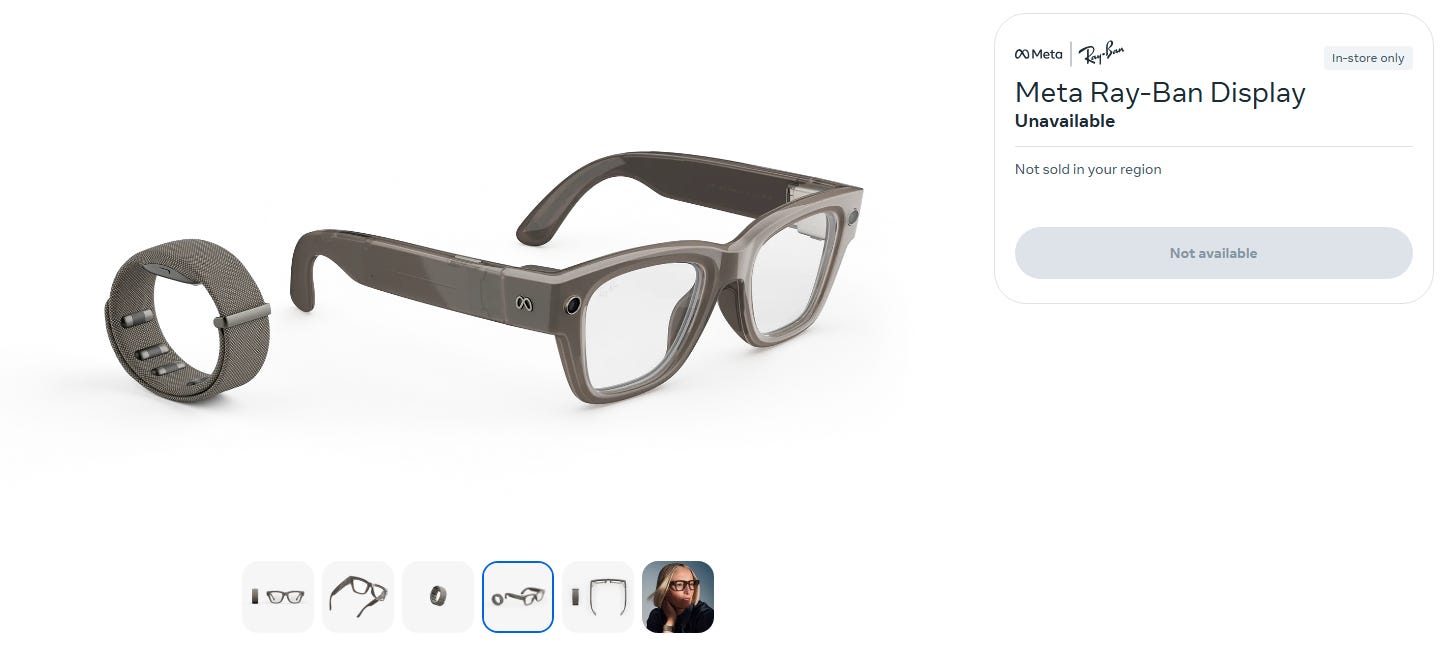
600x600p hi-res full-colordisplay built into the right lens
6-mic arrayand open-ear speakers with Bluetooth connectivity
12MP camerawith 3X zoom and a viewfinder on the in-lens display
Up to 6 hoursof continuous mixed-use battery life per charge and up to 30 total hours of battery life with fully charged case
Amazon’s AR Glasses Bring Hands-Free Efficiency to Delivery Work

Amazon has unveiled an AR smart-glasses prototype designed to make package delivery safer and more seamless by reducing the need for drivers to look down at handheld devices.
According to Amazon, the hands-free system activates only after parking, helping address safety and regulatory concerns. The glasses were developed with feedback from hundreds of delivery drivers and pair with a small vest-mounted controller that includes operational buttons, a swappable battery, and an emergency switch.
The AR display overlays delivery information directly onto the driver’s real-world view—highlighting packages to pick, projecting navigation paths to the doorstep, and prompting photo confirmation after delivery. Future versions may offer real-time hazard alerts such as pets or incorrect addresses, and can support prescription or transitional lenses.

Currently in pilot testing with drivers across North America, the glasses are part of Amazon’s broader effort to modernize logistics through AI and augmented reality, following reports that the company is also exploring consumer AR eyewear to compete with Meta’s Ray-Ban smart glasses.
For Paid Members,SemiVision will discuss topics on
The Rise of SiC Waveguides in AR Glasses
Background: SiC Waveguide for AR Glasses
AR Optical Architectures: A Comparative Overview
Game-Changing Waveguide Materials for AR
Expanding the Field of View in AR Glasses with Silicon Carbide Waveguides
How Waveguides Shape FOV
The Role of SiC Waveguides
Why Silicon Carbide Is Gaining Momentum in Augmented Reality
SiC AR Glasses vs. Traditional Glass AR Glasses: A New Era of Optics
Optical Waveguide Solutions in AR Glasses
SCHOTT and Lumus: innovation fueled by collaboration
Diffractive Waveguides with Surface Relief Gratings
Fundamental Structure of AR Surface Relief Grating (SRG) Waveguides
Diffractive Waveguides with Volumetric Holographic Gratings
PIC Summit Europe: Applied Materials’ Strategic Leap: From Semiconductor Tools to the AI–Optics Interface

The Rise of SiC Waveguides in AR Glasses
Augmented Reality (AR) glasses aim to become as comfortable and effortless to wear as traditional eyewear. Yet, one of the greatest technical challenges remains the display system itself. To succeed, AR devices must deliver displays that are lightweight, compact, and cost-effective—while also meeting the stringent requirements of the human visual system.
Recent research highlights silicon carbide (SiC) waveguides as a promising pathway toward solving these challenges. By enabling ultra-thin, lightweight, and rainbow-free optical components, SiC technology paves the way for AR glasses that are not only more comfortable but also more immersive and visually precise.

Background: SiC Waveguide for AR Glasses
Among various optical solutions for augmented reality (AR) glasses — such as freeform optics, BirdBath, and optical waveguides — the waveguide approach is one of the most promising. Its key advantages lie in being compact, lightweight, and transparent, which makes it possible to design AR glasses that resemble traditional eyewear in form factor while integrating advanced display capabilities.
AR Optical Architectures: A Comparative Overview

- Half Mirror / Beam Splitter (BS) Combiner
This is one of the earliest and simplest AR display architectures. A half mirror or beam splitter directs the light from the display screen into the user’s eye, while still allowing some light from the real world to pass through. Although low-cost and easy to implement, this method suffers from limited transparency, bulkiness, and low efficiency, making it less ideal for consumer-grade AR glasses.
- Birdbath Optics
Birdbath optics rely on a curved partial mirror and a beam splitter to fold and combine the display image with the real-world scene. This approach improves image quality and alignment compared to a simple half mirror. However, it still results in relatively heavy and protruding optics. Birdbath systems are often used in mid-tier AR or VR devices as a compromise between performance and manufacturability.
- Freeform Prisms
Freeform prism optics use precisely shaped prisms to redirect and combine the microdisplay image into the user’s field of view. This enables higher optical efficiency and better visual clarity compared to Birdbath optics. However, freeform prisms are complex to design and manufacture, which drives up cost and limits scalability. They remain a transitional solution for AR headsets but are not well suited for lightweight consumer glasses.
- Waveguide with Grating Couplers
Waveguides represent the cutting edge of AR optics. By using diffraction gratings as in-couplers and out-couplers, light from a microdisplay is injected into a transparent waveguide, guided via total internal reflection (TIR), and then extracted toward the eye. This method allows AR glasses to remain lightweight, thin, and transparent—closely resembling normal eyewear. Waveguides also support a wide field-of-view and high transparency, though they require advanced manufacturing processes and precise materials such as glass or SiC.
- Video See-Through AR Display
In a video see-through system, cameras capture the real world, which is then digitally combined with virtual imagery and displayed to the user. While this allows high flexibility in blending real and virtual elements, it introduces latency, reduces realism, and makes the system bulkier due to camera integration. It is more commonly used in VR or mixed-reality headsets than in lightweight AR glasses.

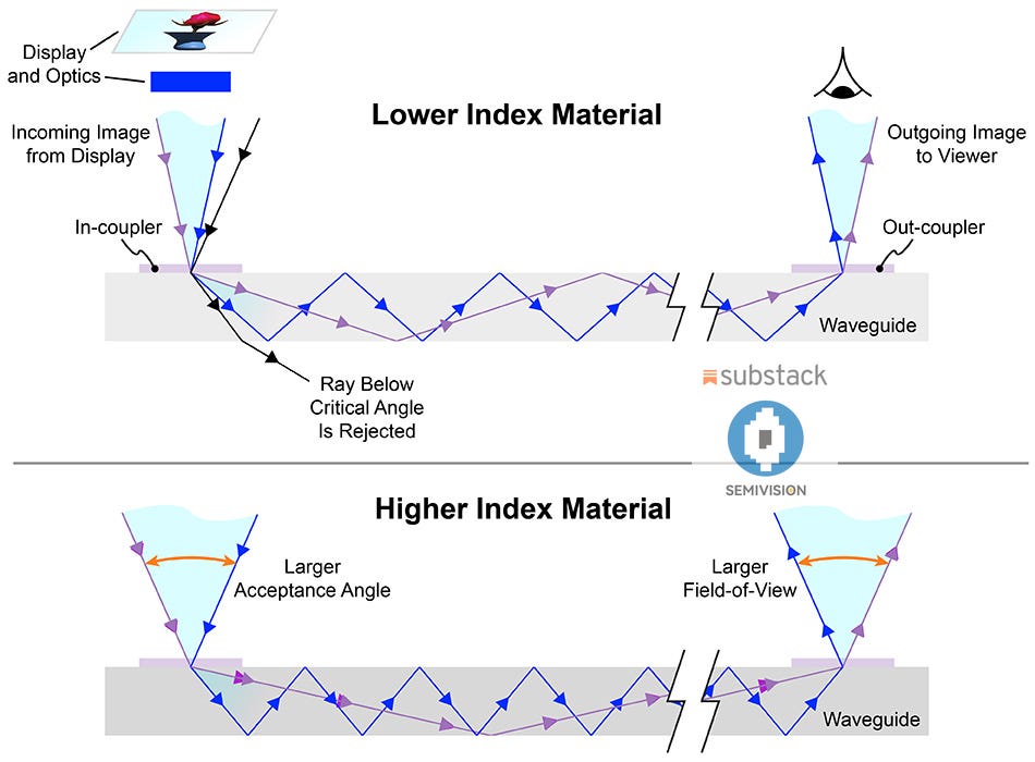
The waveguide principle relies ontotal internal reflection (TIR), where light rays are confined and guided within a transparent medium, effectively acting like a tiny optical channel. Through this mechanism, light from the display is directed into the wearer’s eyes with high efficiency.
When light travels from a material with a higher refractive index (such as glass) into a medium with a lower refractive index (such as air), TIR occurs if the angle of incidence is greater than a certain threshold, known as thecritical angle. At or beyond this angle, the light ray is completely reflected back inside the material. The higher the refractive index contrast, the smaller the critical angle, enabling more efficient confinement of light within the waveguide.
This fundamental property underpins the working principle of waveguide-based AR optics, making them a practical solution to balance thinness, transparency, and optical performance.
Game-Changing Waveguide Materials for AR
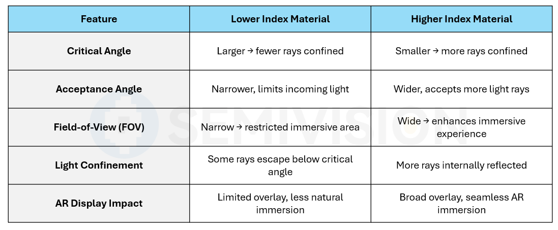
Waveguides in AR systems operate on the principle oftotal internal reflection (TIR). When light travels within a material, it reflects internally if it hits the surface at angles greater than thecritical angle. The key factor here is therefractive indexof the waveguide material.
In alower index material, the critical angle is relatively large. This means only a smaller portion of light rays can be confined within the waveguide, leading to a narrower acceptance angle and, ultimately, a limited field-of-view (FOV). As a result, some light rays fall below the critical angle and escape, reducing the immersive quality of the display.
By contrast, ahigher index materialreduces the critical angle, allowing light to be reflected internally even at steeper incident angles. This expands the acceptance angle, enabling awider field-of-viewto be delivered to the user. For AR glasses, a larger FOV is critical to creating a more natural and immersive visual experience, as it allows virtual content to seamlessly overlay the real world across a broader visual range.
In short, choosing waveguide materials with a higher refractive index — such as SiC or specialized glass — is essential to overcoming optical limits and advancing next-generation AR displays.
Expanding the Field of View in AR Glasses with Silicon Carbide Waveguides
Augmented Reality (AR) glasses are evolving rapidly, and one of the most critical design challenges lies in achieving a wideField of View (FOV). FOV determines how much of the digital world can be overlaid onto the real world at once. A narrow FOV feels like peering through a keyhole, while a wide FOV delivers an immersive, natural visual experience—crucial for applications in gaming, navigation, industrial training, and healthcare.
How Waveguides Shape FOV

Most modern AR headsets useoptical waveguidesto channel light from a micro-display to the wearer’s eyes. Light enters the waveguide through an in-coupler, bounces internally via total internal reflection (TIR), and finally exits through an out-coupler toward the retina. The material properties of the waveguide directly affect how efficiently light can travel and, importantly, how wide the FOV can be.
Withlow-index materials, light can only reflect within a limited angular range. Rays that fall below the critical angle are rejected, which restricts the acceptance angle and narrows the FOV. By contrast,higher-index materials—such as silicon carbide (SiC)—allow light to reflect at steeper angles. This widens the acceptance cone and enables a much broader field of view.
Why FOV Matters
A large FOV is not just a technical metric; it defines the quality of immersion. In AR applications:
30° FOVfeels restricted, suitable only for simple notifications.
40°–60° FOVallows comfortable interaction with digital objects.
80°+ FOVbegins to approach the natural human viewing experience, making digital overlays feel seamlessly integrated into the real world.

For AR to gain mass adoption, users must feel that digital content is not floating in a narrow window but expanding naturally within their sight.
The Role of SiC Waveguides
Silicon carbide offers a high refractive index, mechanical robustness, and thermal stability. By enabling broader reflection angles, SiC waveguides can unlock wider FOVs without compromising image clarity. In practice, this means AR glasses could deliver immersive holographic experiences in a form factor as compact as a pair of reading glasses.
Moreover, SiC’s durability makes it attractive for consumer electronics, where lenses must endure daily wear, scratches, and environmental stress.
The race for immersive AR will be determined not only by processing power or display resolution, but byoptical breakthroughs. Expanding FOV is the key to making AR truly compelling. Materials such as silicon carbide waveguides may represent the next leap forward—bridging the gap between today’s limited AR experiences and tomorrow’s fully immersive digital-physical world.
Why Silicon Carbide Is Gaining Momentum in Augmented Reality
Augmented Reality (AR) glasses are evolving from bulky prototypes into lightweight, everyday wearables. A key enabler of this transformation is the material used in optical waveguides, which guide light from the display into the user’s eyes. Recently,silicon carbide (SiC)has emerged as a highly promising material, offering performance advantages that could redefine the future of AR devices.
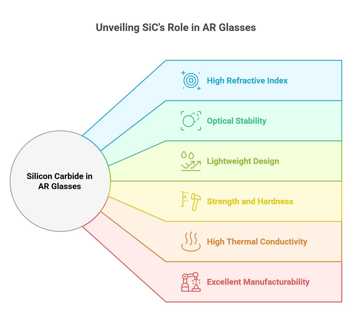
- High Refractive Index (2.6–2.7)

Therelationship between display field-of-view (FOV)and thewaveguide refractive index.
X-axis: Waveguide refractive index
Y-axis: Display field-of-view (degrees)
The trend shows that as the refractive index of the waveguide material increases, the achievable FOV also expands:
High Index Glasses: With a refractive index around 1.7–2.0, the corresponding FOV ranges from about 15° to 30°.
LiNbO₃ (Lithium Niobate): At a refractive index of ~2.3, the FOV reaches around 45°.
SiC (Silicon Carbide): With a refractive index of ~2.6–2.7, the FOV exceeds 60°.
Interpretation
A higher refractive index allows light to undergo total internal reflection at larger angles, enabling a wider FOV in AR waveguides.
This is crucial for AR optical design: choosing higher-index materials such as LiNbO₃ or SiC significantly enhances immersion and visual coverage.
However, challenges remain, as high-index materials often come with greaterfabrication complexity, cost, and long-term reliability issues.

High Index Glassis cost-effective but limits AR to narrow FOV.
LiNbO₃offers wider FOV and potential tunability but with higher cost and fragility.
SiCenables the widest FOV with strong mechanical and thermal advantages, but itsscalability and costremain major hurdles.
- Optical Stability
SiC waveguides resist optical distortions such as ghosting or scattering, resulting in purer and more accurate images. This stability ensures a comfortable viewing experience, reducing eye strain during extended use—a critical factor for consumer adoption.
- Lightweight Design
With relatively low density, SiC lenses are extremely light. A single SiC waveguide lens can weigh as little as2.7 grams, which is essential for long-duration wear without discomfort.
- Strength and Hardness
SiC is second only to diamond in hardness, reaching a Mohs hardness of9.5. This outstanding mechanical strength makes it highly resistant to scratches, wear, and environmental stress. For AR glasses—products meant to be worn daily—durability is just as important as optical performance.
- High Thermal Conductivity (490 W/m·K)
SiC dissipates heat exceptionally well, ensuring that optical properties remain stable even under high-temperature conditions. This also helps mitigate issues such as the “rainbow effect” often seen in waveguide displays, thereby improving image uniformity and clarity.
- Excellent Manufacturability
Beyond performance, SiC can beprecisely processed into complex shapes and dimensionswith high accuracy. This gives manufacturers flexibility in customizing designs for different AR applications, from consumer glasses to industrial headsets.
The rise of AR is not only about advances in display engines, processors, or software—it is equally about breakthroughs inmaterials science. Silicon carbide’s unique combination of high refractive index, optical stability, durability, thermal conductivity, and manufacturability positions it as a front-runner for next-generation AR waveguides.
As AR moves closer to mass adoption, SiC may be the material that bridges the gap between today’s limited devices and tomorrow’s fully immersive AR glasses.
SiC AR Glasses vs. Traditional Glass AR Glasses: A New Era of Optics
As augmented reality (AR) moves toward mainstream adoption, the choice of lens material is becoming a decisive factor. Traditional AR glasses have long relied on multi-layered glass waveguides. However,silicon carbide (SiC)is emerging as a superior alternative, offering dramatic improvements in weight, thickness, optical performance, and manufacturability.
Lightweight and Ultra-Thin Design
One of the most striking differences is weight. A singleSiC AR lens weighs only 2.685 grams, compared with10–15 grams for traditional glass lenses—an80% reduction. This makes AR glasses far more comfortable for long-term wear.
Superior Optical Performance
Traditional glass waveguides often suffer from rainbow artifacts due to theirlower refractive index (1.8–2.0)andlarger grating period (370–400 nm). By contrast, SiC offers ahigher refractive index of 2.6and ashorter grating period of 262 nm, eliminating rainbow distortions and delivering purer, sharper full-color displays.
Additionally, SiC lenses integrate optical corrections directly, thanks to ultra-thin Fresnel structures bonded to the waveguide surface. This eliminates the need for external corrective lenses, further reducing bulk and weight.
Thermal and Structural Advantages
SiC’shigh thermal conductivityoutperforms glass, reducing the risk of thermal hotspots and ensuring stable performance under extended use. This feature is vital for AR devices, where localized heating from display engines and processors can degrade optical quality.
Structurally, SiC’s hardness approaches that of diamond, making it far more scratch-resistant and durable than conventional glass. This enhances long-term reliability for consumer and industrial applications alike.
Manufacturing Compatibility
Traditional glass waveguides face challenges in mass production due to resin deformation during thermal processes. SiC, however, is highly compatible withsemiconductor-grade manufacturing, leveraging 4-inch SiC wafers and established fabrication methods. This opens the door to scaling AR production with higher consistency and precision.
A Clear Winner for Next-Generation AR
In summary,SiC AR lenses deliver unmatched performanceacross multiple dimensions:
Weight:2.7 g vs. 10–15 g (traditional glass)
Thickness:0.55 mm vs. 2–3 mm
Optical Quality:No rainbow artifacts, sharper images
Integration:Built-in Fresnel corrections, no external lens required
Durability:Near-diamond hardness, superior heat dissipation
These advantages position SiC not just as an incremental improvement, but as a transformative material that could redefine the future of AR optics. For AR glasses to move from niche to mainstream, breakthroughs in comfort, clarity, and manufacturability are essential—and SiC may provide the pathway.

The picture above illustrates a comparison betweensilicon carbide (SiC) waveguides(left) andconventional multi-layer glass waveguides(right). SiC waveguides are significantly thinner and lighter, achieved by combining an ultra-thin SiC optical layer with prescription glass. This design reduces overall device weight while improving integration with corrective optics.
A key advantage of SiC is itshigher refractive index and superior thermal conductivity, which allow efficient light guiding, stable optical performance under heat, and reduced risk of thermal hotspots. Importantly, SiC waveguides eliminate therainbow artifactscommonly observed in glass-based systems, enabling a clearer and more natural full-color display.
By contrast, traditional glass waveguides require multiple stacked layers, resulting in greater thickness and weight. They also suffer from scattering effects and chromatic distortions, reducing display clarity.
In short, the SiC platform not only enhances user comfort with a lightweight, slim form factor, but also delivers superior image quality and thermal stability—key requirements for the next generation of immersive AR glasses.

The photographs illustrate thepractical performance of SiC-based AR glasses. On the left, the test setup shows the glasses in hand, projecting a vivid image directly onto the user’s field of view. Unlike traditional glass waveguides that often suffer from low brightness and color washout, the SiC platform maintains clarity and vibrancy.
On the right, two sets of comparisons are shown. At thetop, full-color images of flowers, butterflies, and landscapes are displayed in adarkroom environment, highlighting the precision and sharpness of the projection. The displays show excellent color fidelity with deep contrast, free from rainbow artifacts.
At thebottom, the same content is tested in adaytime environmentunder bright ambient lighting. Even in such conditions, the SiC waveguide delivers strong brightness and saturated colors, ensuring that AR content remains visible and immersive. This is a major advancement since brightness and visibility in daylight have been long-standing challenges for AR devices.
Together, these results demonstrate that SiC AR glasses not only excel in laboratory conditions but also perform reliably in real-world scenarios—bridging the gap between research prototypes and practical, consumer-ready AR experiences.
Optical Waveguide Solutions in AR Glasses
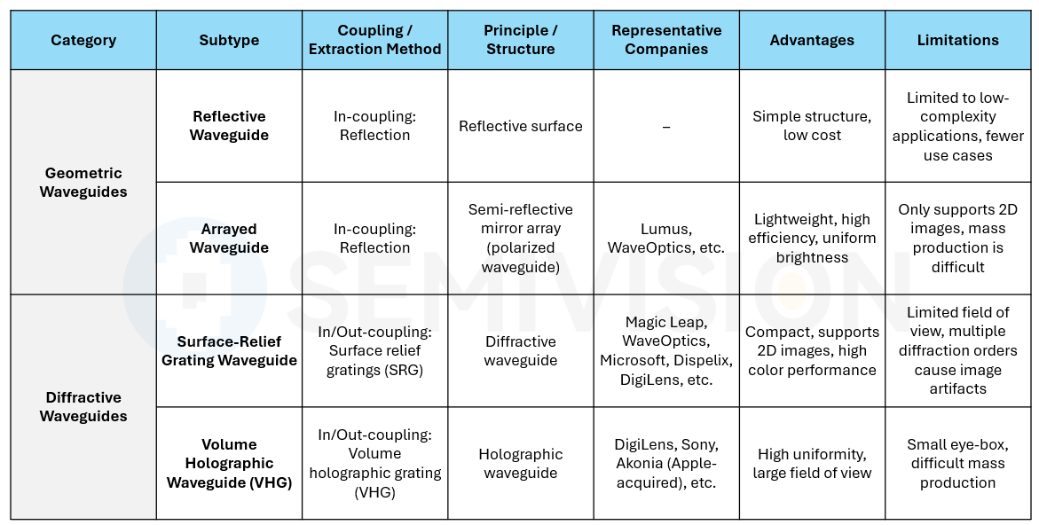
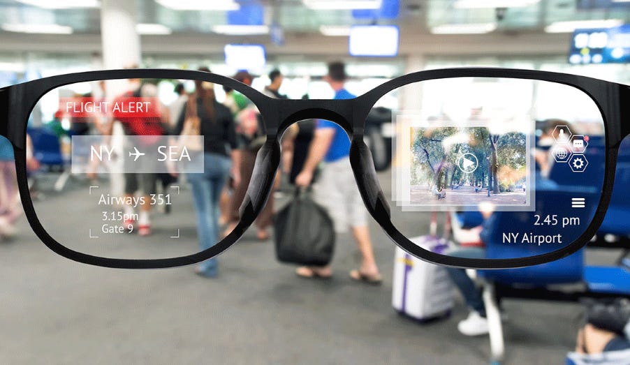
In AR glasses, optical waveguide solutions stand out as the most promising approach due to their advantages in compactness, light transmittance, clarity, and field of view (FOV). Waveguide-based AR systems typically consist of three key components: a display module, a waveguide plate, and coupling elements. Light emitted from the display module is coupled into the waveguide, propagates forward through total internal reflection, and is eventually out-coupled toward the human eye to form an image.
Array waveguidesoffer excellent imaging performance. Their two-dimensional pupil-expansion schemes address the trade-off between optical engine size, FOV, and eye-box. However, the challenges of large-scale manufacturing remain significant.
Surface-relief grating (SRG) waveguidesare produced using nanoimprint technology. Compared with array waveguides, they are relatively easier to mass-produce, but challenges remain—such as rainbow artifacts, low optical efficiency, and limited FOV. Notably, this is the waveguide approach with the largest number of domestic suppliers in China.
Volume holographic waveguides (VHGs)hold strong theoretical advantages, with higher diffraction efficiency, better imaging quality, and potentially lower production costs. The main bottleneck lies in the choice and preparation of holographic materials, as large-scale production requires strict material and process control. Domestic suppliers active in this domain.
Geometric Arrayed Waveguides in AR Glasses
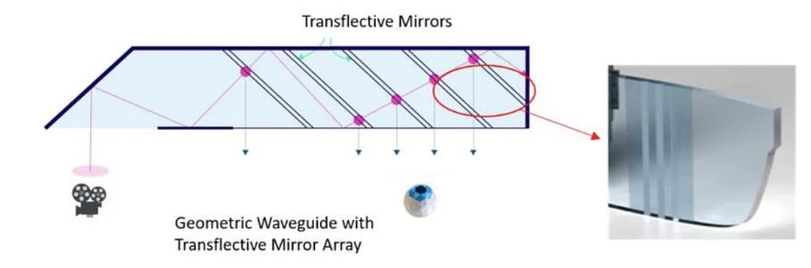
Geometric arrayed waveguides achieve image output and pupil expansion through an array of stacked reflective mirrors. A leading optical company working on this approach isLumusfrom Israel.

The optical path design works as follows: light from the display module is coupled into the waveguide through reflective surfaces or prisms. Inside the waveguide, a series ofsemi-reflective, semi-transparent mirrorssequentially extract the light, guiding it outward toward the user’s eye. Unlike diffractive or holographic solutions, geometric waveguides do not rely on micro- or nano-scale structures. As a result, they can deliver high-quality images with excellent color fidelity and contrast.
However, manufacturing challenges remain. Each semi-reflective mirror requires deposition of dozens of thin-film coating layers. This complex process reduces yield rates, making large-scale mass production difficult.
Advantages
High image quality with excellent color and contrast
No dependence on micro- or nano-scale structures
Mature optical principles, straightforward light path design
Disadvantages
Requires complex multilayer coatings for each mirror
Low manufacturing yield
Limited scalability for high-volume mass production
Representative company
SCHOTT and Lumus: innovation fueled by collaboration
Between the two companies is an ongoing exchange - new ideas, designs, and capabilities are conceptualized, converted into products, and pressure tested to see what is manufacturable on an industrial scale. Where Lumus’s job is developing groundbreaking designs for potential AR see-through-displays, SCHOTT’s job is to make them a reality – and that goes far beyond supplying glass wafers to produce finished waveguides ready for AR devices.
Diffractive Waveguides with Surface Relief Gratings
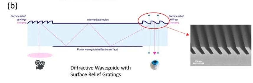
Unlike geometric waveguides, which rely on arrays of reflective mirrors,diffractive waveguidesuse grating structures to expand and out-couple light beams. Depending on how the gratings are fabricated, diffractive waveguides can be categorized intosurface relief grating (SRG) waveguidesandvolume holographic grating (VHG) waveguides.

Devices such as Microsoft HoloLens 2 and Magic Leap One employ surface relief grating waveguides. These rely on binary optics theory and are manufactured using nanoimprint lithography to create highly precise structures directly on the wafer surface. Depending on the design, surface relief gratings can take different forms, including rectangular, slanted, or blazed gratings.
The key advantage of this approach is that it does not require embedding complex multi-layer coatings inside the lens, as with geometric waveguides. Instead, the grating structure is directly fabricated on the lens surface, simplifying the process. This makes SRG waveguides relatively easier to mass-produce, with lower production costs and strong scalability for future applications.
Advantages
Simpler fabrication compared to geometric waveguides
Supports nanoimprint lithography for high precision
Lower mass production cost
Strong scalability and commercial adoption (e.g., HoloLens 2, Magic Leap One)
Disadvantages
Optical efficiency remains limited
Image artifacts such as rainbow patterns may occur
Field of view (FOV) is typically narrower than desired

Fundamental Structure of AR Surface Relief Grating (SRG) Waveguides
The basic architecture of AR surface relief grating (SRG) waveguides consists of three key components: thesubstrate, thesurface relief grating structure, and thecover layer.
Substrate: Serves as the supporting medium and provides the foundation for optical transmission.
Surface Relief Grating: The core element of the waveguide. Periodic nanoscale grating patterns are formed on the substrate surface through lithography and etching, enabling precise control of light propagation.
Cover Layer: Protects the grating structure while optimizing optical performance.

Key Thin-Film Materials in SRG Fabrication
- TiO₂ – Core Optical Material of SRGs
Titanium dioxide (TiO₂) is widely used due to its high refractive index (2.4–2.6 at 550 nm) and low absorption in the visible spectrum. This high refractive index contrast with surrounding low-index materials allows light to be confined within the waveguide through total internal reflection. The result is reduced leakage and scattering, leading to improved transmission efficiency and image quality.
- Cr – Reliable Hard Mask Material
Chromium (Cr) is highly valued for its chemical stability and etching selectivity. In SRG fabrication, a thin Cr layer is deposited on the substrate, patterned via photolithography, and then used as a hard mask during etching. This process enables precise pattern transfer onto TiO₂, ensuring accurate nanoscale structuring of the gratings.
- Al – High-Performance Metallic Filler
Aluminum (Al) is often introduced as a filler material to enhance both optical and mechanical properties of SRGs:
Optical performance:Al has excellent reflective characteristics. When integrated into TiO₂ gratings, it increases reflectivity for specific wavelengths, improves diffraction efficiency, and reduces transmission/absorption losses. By tuning the Al thickness, grating dimensions, and TiO₂–Al configuration, selective wavelength reflection and spectral modulation can be achieved.
Mechanical stability:TiO₂ is hard but brittle, whereas Al provides ductility and toughness. Filling Al into TiO₂ gratings enhances structural robustness, reduces surface damage from friction or scratches, and improves product yield and durability.
AR surface relief grating waveguides represent a balance of advanced nanofabrication, material science, and optical engineering. TiO₂ ensures strong light confinement, Cr guarantees precise pattern transfer, and Al enhances both optical efficiency and mechanical reliability. Together, these elements form the foundation for scalable, high-performance AR display solutions.
Diffractive Waveguides with Volumetric Holographic Gratings
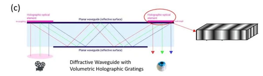
Compared with geometric waveguides, diffractive waveguides have the advantage of enabling two-dimensional pupil expansion (2D exit pupil expansion). Traditional imaging systems usually provide only one image exit point, meaning the user’s eye must remain aligned to see the image. By using semi-reflective mirrors or grating structures, diffractive waveguides can create multiple exit points. This allows the image to remain visible even as the eye moves horizontally, effectively achieving one-dimensional pupil expansion.
Going further, by carefully designing the grating structure—often in a hexagonal arrangement of cylindrical gratings—diffractive waveguides can achieve two-dimensional expansion. This significantly enlarges the effective field of view, making the display more user-friendly and immersive. The semiconductor fabrication process for such gratings is relatively straightforward, making large-scale production more cost-efficient.
A more advanced form of this technology is the volumetric holographic grating (VHG) waveguide, which uses holographic optical elements (HOEs) instead of surface relief gratings. Companies like Akonia (acquired by Apple) have pioneered this approach. HOEs are created by dual-beam laser holographic exposure, forming nanoscale grating structures directly within a photosensitive polymer film at the micrometer scale. This method produces gratings with high transparency and high diffraction efficiency, resulting in superior color performance and image quality compared to SRG waveguides.
However, VHG waveguides face significant challenges. The preparation of holographic materials is complex, mass production is difficult, and long-term stability and reliability of the materials are still uncertain.
Advantages
Enables two-dimensional pupil expansion, greatly enhancing the field of view
Lower production costs compared to geometric waveguides
HOEs provide high transparency and high diffraction efficiency
Better color reproduction and image quality than SRG-based waveguides
Disadvantages
Complex material preparation and processing requirements
Difficult to scale for high-volume mass production
Long-term material stability and reliability remain concerns
The rise of AI technologies is driving terminal innovation, with AI smart glasses emerging as a new vehicle for AI adoption. Compared with traditional XR devices, AI smart glasses integrate AI capabilities while focusing primarily on vision and hearing functions. Without the bulky optical systems of XR products, they are lighter, more comfortable to wear, and better suited for daily-life scenarios. This also reduces the sense of “device boundaries,” making usage more natural. Today, users primarily rely on AI smart glasses for photo capture, first-person livestreaming, music playback, phone calls, and AI voice interaction.
As AI development shifts increasingly toward consumer endpoints, AI smart glasses—combining vision, hearing, and language, the most important sensory channels for human interaction—are expected to become a key platform for real-world AI applications.
With more players entering the market, 2025 is likely to see an intensive wave of AI smart glasses product launches. The category is gradually shifting from “tech showcase” to practical tools, with functions such as translation, photo capture, and AI voice assistants becoming high-frequency daily-use scenarios. In activities such as sports, commuting, and translation, AI glasses hold the potential to partially replace smartphones. In addition to traditional XR hardware makers, internet companies and consumer electronics brands are also entering this space. According to SemiVision’s forecast, global AI smart glasses shipments are expected to reach 5.5 million units in 2025, growing to 22 million units by 2027, representing a CAGR of 144% from 2024 to 2027.
Looking ahead, the combination of AI + AR unlocks even greater application potential, with SoCs and optical display systems becoming the core value drivers. Based on Wellsenn’s teardown data, the Ray-Ban Meta smart glasses carry a BOM cost of about USD 164, with the largest share concentrated in chip components (52%), where the SoC is the main cost source. In the future, smart glasses with integrated display functions will enable broader, more imaginative application scenarios, maximizing the innovation potential of AI technologies. Compared with AI-only smart glasses, AI+AR glasses add optical display modules as a key incremental component. As optical display technology advances and the supply chain matures, Micro LED + waveguide solutions are expected to become a critical trend.

PIC Summit Europe:Applied Materials’ Strategic Leap: From Semiconductor Tools to the AI–Optics Interface

Applied Materials’ PIC Summit Europe presentation marks not just a product discussion — it signals a strategic redefinition of its role in the AI hardware ecosystem. Long recognized as the world’s largest semiconductor equipment supplier, Applied is now positioning itself beyond its traditional domain of “tools that manipulate electrons” to enter a new frontier: nanostructures that manipulate photons.
This shift reflects a deeper thesis — that smart glasses will become the next essential interface for Artificial Intelligence (AI). While today’s AI interaction still relies on flat screens and command-line–like text prompts, Applied believes that the future interface must be head-mounted, visual, and ambient — allowing humans to see, show, and speak to AI naturally.
From Vision Pro to Vision Light
The company’s platforms business argues that despite their technical brilliance, devices such as Apple Vision Pro and Magic Leap remain too bulky for continuous use. What the market truly needs are lightweight, everyday glasses that serve as both optical displays and AI terminals.
This perspective reframes smart glasses from being a “wearable gadget” to becoming a foundational interface layer of the AI era — one that merges perception, display, and context awareness into a seamless human–machine loop.
Engineering the Invisible

From a manufacturing standpoint, Applied’s move is profound. Instead of merely selling capital equipment, the company is now developing and commercializing optical waveguides and photonic display components — the invisible layers that make near-eye projection possible.
These components require atomic-level control over high-refractive-index materials, deposited, etched, and patterned using advanced semiconductor tools. The engineering paradox is elegant: massive process complexity invested in creating a surface that, if successful, is literally invisible to the user.

Unlike chip wafers that aim for perfect uniformity, optical substrates for eyewear must be both scalable and personalized, tuned to individual facial geometry, interpupillary distance, and prescription correction. Applied’s new Singapore fabrication facility, developed jointly with GlobalFoundries, will address precisely this challenge — mass-producing millions of unique yet optically precise parts.
Applied Materials and GlobalFoundries Partner to Accelerate AI-Powered Photonics
Photonics Meets Semiconductor Discipline

Applied Material’s presentation delved into the structure of surface-relief gratings used in waveguides — microscopic patterns that diffract, replicate, and steer light through total internal reflection to generate an image in the user’s eye.
Here, Applied’s semiconductor DNA is a clear advantage:
Material controlat the atomic level determines color uniformity and brightness.
Metrology precisionensures optical contrast and defect invisibility.
Process integrationenables yield at scale, something photonics startups have long struggled to achieve.
In essence, Applied is attempting toindustrialize nanophotonic manufacturingwith the same discipline that once scaled transistors.
System-Level Co-Optimization
Beyond materials and optics, the company is building reference designs integrating waveguides, lenses, sensors, and light engines into a sub-50-gram prototype. The optical engine projects an image at infinity, corrected by stacked prescription and compensating lenses to maintain realistic depth perception and visual comfort — a critical ergonomic factor for mass adoption.
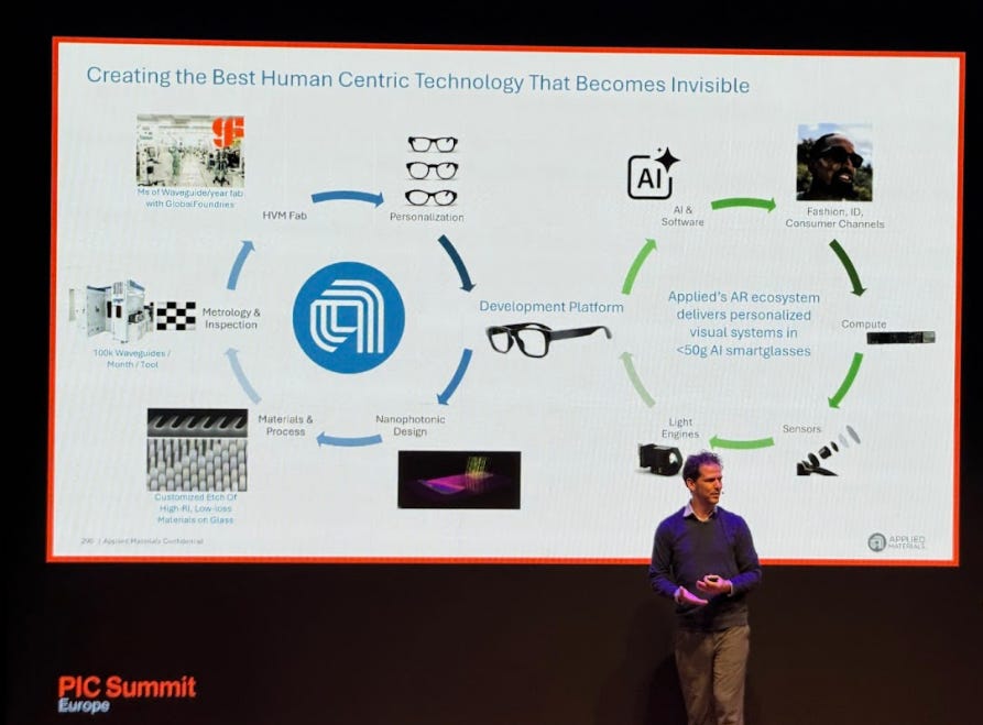
Engineering the Invisible Loop
An elegant vision of what it calls the “Invisible Loop” — a closed ecosystem in which each stage of development strengthens the next, ultimately merging advanced materials science with human-centered design. The loop begins at the materials and process level, where high-refractive-index, low-loss materials are precisely etched on glass to create nanostructures that manipulate photons with the same precision used to control electrons in semiconductors. These structures are then shaped through nanophotonic design, forming transparent surface-relief gratings that guide light and project digital images directly into the human eye. To ensure optical perfection, metrology and inspection systems measure waveguide contrast, color uniformity, and field accuracy—making sure that defects invisible to a chip remain invisible to the wearer as well.
The loop then scales into high-volume manufacturing, where Applied, in partnership with GlobalFoundries in Singapore, aims to produce millions of waveguides annually—approximately 100,000 units per tool per month. Yet unlike chips, every optical element must be personalized to fit an individual’s facial geometry, requiring a manufacturing architecture capable of mass-customizing millions of unique SKUs. These optical components converge within a development platform that integrates compute, light engines, and sensors into a sub-50-gram smart-glasses system. On top of this hardware, AI and software layers deliver contextual intelligence, learning from each user’s behavior and surroundings. Finally, success depends on fashion, industrial design, and consumer channels—ensuring that these AI-driven glasses are not only powerful but also something people genuinely want to wear.
Together, these interlocking stages define Applied’s vision of engineering technology that ultimately disappears—a seamless interface where computation, optics, and human experience become one continuous, invisible loop.
Strategic Implications
From a SemiVision perspective, Applied’s initiative represents a horizontal expansion of the semiconductor value chain — from electron devices (logic and memory) to photon devices that directly mediate human–AI interaction.
This strategy aligns with three broader industry trends:
Photonics convergence– integrating optical computation and communication into the AI ecosystem.
Vertical integration of system IP– equipment firms moving closer to end-application components.
Localized, scalable production– Singapore’s fab serving as a blueprint for future “AI optics foundries.”
In the long term, Applied’s move suggests that the next competitive frontier in AI hardware will not only be in GPU or NPU performance, but also in the optical interfaces through which intelligence manifests. Whoever controls the “AI viewport” — the way humans see and experience artificial cognition — will shape the next decade of computing.

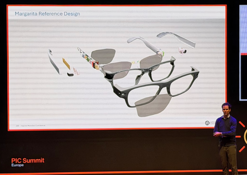
At the PIC Summit Europe, Applied Materials unveiled its first smart-glasses reference design, codenamed“Margarita.”The prototype represents the company’s most concrete step toward realizing its vision of human-centric, AI-integrated eyewear. Developed in collaboration with Avegant and powered by Qualcomm’s Snapdragon AR1 platform, Margarita weighs just 45 grams and integrates a full-color, 20° field-of-view display delivering 3,000 nits of brightness at 38 pixels per degree — specifications approaching the threshold for real-world, outdoor-visible augmented displays.
Applied’s contribution lies in its high-performance etched waveguide (WG) technology, fabricated with the same semiconductor-grade precision that defines its process tools. The waveguide incorporates integrated lenses, co-optimized with Avegant’s AG 2.0 light engine, ensuring a compact optical stack with high brightness and minimal distortion. On the functional side, the glasses feature a 13 MP camera with display overlap, a low-power always-on MCU, Wi-Fi 6 / Bluetooth 5.3 LE connectivity, directional stereo speakers, a beam-forming microphone array, and a 200 mAh battery with USB-C charging — all within a sub-50 g frame.
Unlike earlier AR headsets designed for immersion, Margarita prioritizes wearability and contextual intelligence — enabling AI assistance through natural, lightweight interaction. As Applied Materials transitions from supplying semiconductor tools to developing optical systems and AI hardware platforms, this reference design marks a pivotal milestone. Development kits are now available for pre-order, signaling the company’s intention to foster a broader ecosystem of partners across optics, compute, and consumer design — bringing the vision of truly invisible AI technology one step closer to reality.
Applied Materials’ transition from process equipment to photonic component manufacturing is not a side project — it’s a strategic prototype of how semiconductor infrastructure will extend into the human–AI interface layer.
By bringing semiconductor precision to optics, Applied is effectively bridging the gap between the fab and the face — turning photons into the next substrate for AI.


PreviousNext
TopLatestDiscussions








See all