The Netherlands — The Next Innovation Hub for Integrated Photonics
The Netherlands — The Next Innovation Hub for Integrated Photonics
- Source: SemiVision
- Author: SEMIVISION
- Published: 2025-10-24T11:41:41+08:00
- URL: https://tspasemiconductor.substack.com/p/the-netherlands-the-next-innovation The Netherlands — The Next Innovation Hub for Integrated Photonics


The Netherlands — The Next Innovation Hub for Integrated Photonics
Original Article by SemiVision Research (PIC Summit Europe)

Oct 24, 2025
∙ Paid
The Netherlands — The Next Innovation Hub for Integrated Photonics
Just as ASML elevated the Netherlands to the global forefront of lithography, integrated photonics is now driving a new technological revolution. This time, the focus is on photonic chips, sparking a restructuring of the entire ecosystem spanning design, manufacturing, packaging, and applications. Backed by world-class research, dense industry collaboration, and strong government support, the Netherlands is firmly establishing itself as the global hub for integrated photonics innovation.

The Dutch Integrated Photonics Value Chain: Building the Next ASML-Level Innovation Powerhouse
Against the backdrop of rapid advances in high-performance computing, AI data centers, and communications technologies, integrated photonics has emerged as a key enabler of the next semiconductor revolution. And the Netherlands stands out as one of the epicenters of this transformation. Leveraging ASML’s global dominance in lithography, the country has nurtured a vibrant integrated photonics innovation ecosystem—uniting academia, startups, large industry players, and government institutions. At the heart of this ecosystem is PhotonDelta, the central platform accelerating the industrialization and commercialization of integrated photonic chips (PICs).

Integrated Photonics Ecosystem in the Netherlands. Source : PhotonDelta
A Fully Integrated Photonics Value Chain in Netherlands
From research and development to manufacturing, from design and simulation to testing and validation, the Netherlands has established a comprehensive Integrated photonics value chain:
Materials and Component Manufacturing: Companies such as SMART Photonics (InP platform), Lionix, Chilas, Superlight, and EFFECT Photonics deliver critical devices ranging from lasers and amplifiers to modulators and photodetectors.
Design and Simulation Tools: Luceda Photonics, Synopsys, and Spectrik provide specialized PIC design software and simulation platforms.
Packaging and Assembly: Firms like Phix, BRIGHT Photonics, MicroAlign, and Xiver focus on optoelectronic heterogeneous packaging and passive/active coupling solutions.
Testing and Reliability Verification: ManiSpectra, Brilliance, Epiphany, SURFIX Diagnostics, and the TNO Holst Centre support the ecosystem with advanced testing, validation, and optical performance assessment.
System Integration and Applications: Leading players including NXP, IMEC, ASML, TU/e (Eindhoven University of Technology), and the OnePlanet Research Center drive adoption across applications in AI, 5G, healthcare, and precision measurement.
Most of these companies and research institutions are clustered within a two-hour drive across cities such as Amsterdam, Eindhoven, Enschede, Nijmegen, and Delft, forming a high-density and agile innovation corridor. This concentration creates a uniquely cohesive technology cluster, positioning the Netherlands as a potential birthplace of the “next ASML” in the Integrated photonics era.
Global Alignment: Advancing Taiwan–Netherlands Collaboration
A new wave of international cooperation is taking shape as the Netherlands, through its government and the PhotonDelta program, actively builds bridges with Asia’s semiconductor ecosystem — with Taiwan at the center. Several milestones highlight this deepening partnership:
SEMICON Taiwan 2025 (September 8–12):
The Netherlands delegation, representing sectors from equipment and design to testing and next generation semiconductor technology - including advanced packaging and PICs were hosted at the NL Pavilion. Semicon Taiwan is serving as a hub for bilateral engagement. The event continues to serve as a platform for bilateral engagement between Taiwan and the Netherlands. This year, several key participants from the Dutch PIC ecosystem including PhotonDelta, Eindhoven University of Technology (TU/e), SMART Photonics, and Phix visited Taiwan. These exchanges aim to accelerate and facilitate joint R&D, packaging solutions, and supply chain alignment within the integrated photonics domain.
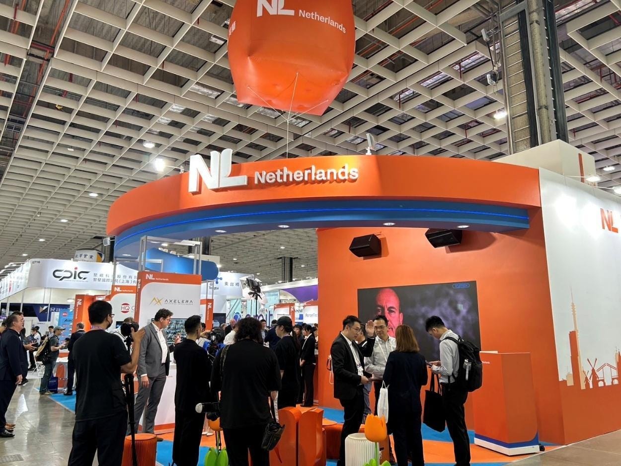
The Netherlands Pavilion participated in SEMICON Taiwan. Source: SemiVision
PIC Summit Europe 2025 (November 4-5):
Recognized as Europe’s largest integrated photonic chip summit, the event’s theme,“Scaling Together in a Dynamic World,”will focus on industry scaling strategies, platform integration, investment landscapes, and global supply chain collaboration. Taiwan’s participation is expected to bring complementary expertise in advanced packaging, testing, and manufacturing capacity, aligning with Europe’s strengths in design, photonics materials, and system applications.
PIC Summite Europe 2025 Website

Source: Picsummiteurope.com
Through these efforts, the Netherlands is signaling its intent to position itself as a global hub for integrated photonics, while ensuring Taiwan becomes a key partner in building resilient, cross-continental innovation ecosystems. This joint momentum not only strengthens industrial collaboration but also creates strategic value chains that can compete on a worldwide scale.
From Lithography to Photonics: Recreating the ASML Model
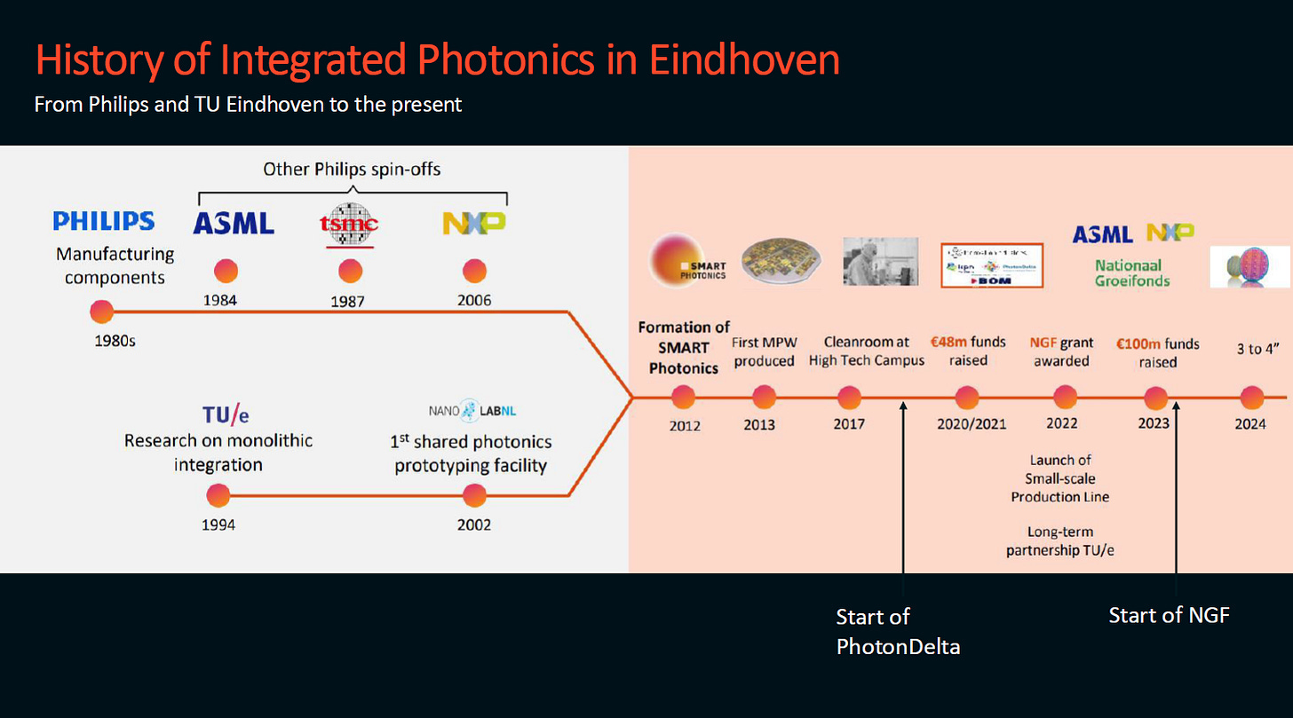
Source: PhotonDelta
The Netherlands’ push into integrated photonics carries with it the ambition of“replicating the ASML model.”Just as ASML revolutionized the semiconductor industry by combining government resources, cutting-edge research, and partnerships with international customers to deliver breakthrough lithography systems, PhotonDelta and its ecosystem partners are now pursuing a similar trajectory. By committing to long-term R&D, standards development, and volume production support, the Netherlands aims to once again secure a pivotal position in the global chip industry.
The Dutch Integrated Photonics Ecosystem: A Full-Chain Joint Launch
Academic and Research Excellence
The Netherlands has built a strong foundation in integrated photonics research through world-leading universities and institutes. Close collaboration among Eindhoven University of Technology (TU/e), University of Twente, Delft University of Technology (TU Delft), TNO Holst Centre, and IMEC ensures that innovations transition seamlessly from academic research to industrial deployment.
These institutions collectively drive advances in indium phosphide (InP), aluminum oxide (AlOx), silicon photonics and more, enabling breakthroughs in chip design, heterogeneous integration, and packaging. Their combined expertise forms the scientific backbone of the Dutch and European photonics ecosystem—linking fundamental research, pilot manufacturing, and commercial innovation.
Beyond Research — Toward Industrial Impact
The Netherlands is not only building a photonics R&D hub but also laying the foundation for industrial-scale production and commercialization. This includes:
Establishing packaging and testing capabilities that mirror the foundry–OSAT model in semiconductors.
Building supply chain standards to ensure interoperability and scalability across Europe and Asia.
Encouraging startups to co-develop with global customers, echoing the “early customer engagement” strategy that propelled ASML’s success.
Strategic Vision
If successful, the Dutch Integrated photonics ecosystem could replicate the transformative role ASML played for lithography — this time in the field of integrated photonics (PICs). By combining academic strength, government investment, and industrial collaboration, the Netherlands is positioning itself as the next indispensable node in the semiconductor revolution, enabling applications across AI, data centers, quantum computing, 5G/6G, and healthcare.
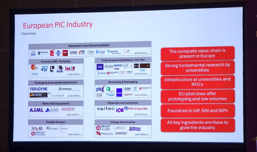
Overview of European PIC Industry. Source: PhotonDelta
Industry Leaders and Innovators in NL
SMART Photonics (Eindhoven): An InP PIC foundry that completed a €100 million capital raise in 2023, backed by ASML, NXP, and the Dutch government, positioning itself as the cornerstone of Europe’s integrated photonics manufacturing capability.
Companies such as EFFECT Photonics and PHIX, specializing in advanced packaging and coupling technologies, have also benefited from PhotonDelta’s ecosystem funding and strategic connections, enabling them to scale toward global markets.
Infrastructure and Startup Acceleration
High Tech Campus Eindhoven: A dense innovation hub hosting over 300 high-tech companies and 13,000 R&D professionals. Located adjacent to ASML’s headquarters, the campus serves not only as the beating heart of the Dutch semiconductor industry but also as a fertile ground for new integrated photonics startups.
PhotonDelta has also extended its reach across the Atlantic, partnering with Silicon Catalyst (USA) and Luminate NY, building a transatlantic acceleration chain to nurture early-stage photonics ventures.
Government and EU Financial Backing
The Netherlands’ National Growth Fund has committed €470 million to support the development of its integrated-photonics ecosystem via PhotonDelta. Separately, the EU (via the Chips JU/EU Chips Act framework) will contribute approximately €133 million toward photonic semiconductor pilot-production facilities in the Netherlands. A key element of this push is a new6-inch Indium-Phosphide (InP) pilot lineat TNO’s High Tech Campus in Eindhoven, which is regarded as a major milestone for both the Dutch and European photonics industries.
The PhotonDelta Startup Fund provides early-stage loans ranging from €250,000 to €2 million, reducing the barriers for startups to move from concept to commercialization.
Dutch municipalities are also playing an active role, driving “smart city” innovation programs that reinforce international collaboration and anchor the Netherlands as a global hub for photonics.
This synergy of industry leaders, research institutions, startups, and government investment mirrors the collaborative model that propelled ASML to global dominance. With its clear roadmap, financial muscle, and international alliances, the Netherlands is positioning itself as the epicenter of integrated photonics innovation, securing a decisive role in the future of global semiconductor technology.
From the Kingdom of Lithography to the Age of Photonics
The Netherlands is now working to replicate the ASML model in the next frontier of information technology: Photonic Integrated Circuits (PICs). With leadership from PhotonDelta, SMART Photonics, Phix, and Eindhoven University of Technology (TU/e), the country is accelerating the construction of a complete photonics ecosystem spanning materials, design, manufacturing, packaging, testing, and applications.
Much like its leadership in EUV, the Netherlands is once again igniting a new technological revolution. In emerging domains such as AI servers, quantum communications, edge computing, and LiDAR sensing, Integrated photonics could become just as critical as EUV in defining the industry’s future. The Netherlands is well positioned to once again take the lead and become the world’s next “Capital of Photonics.”
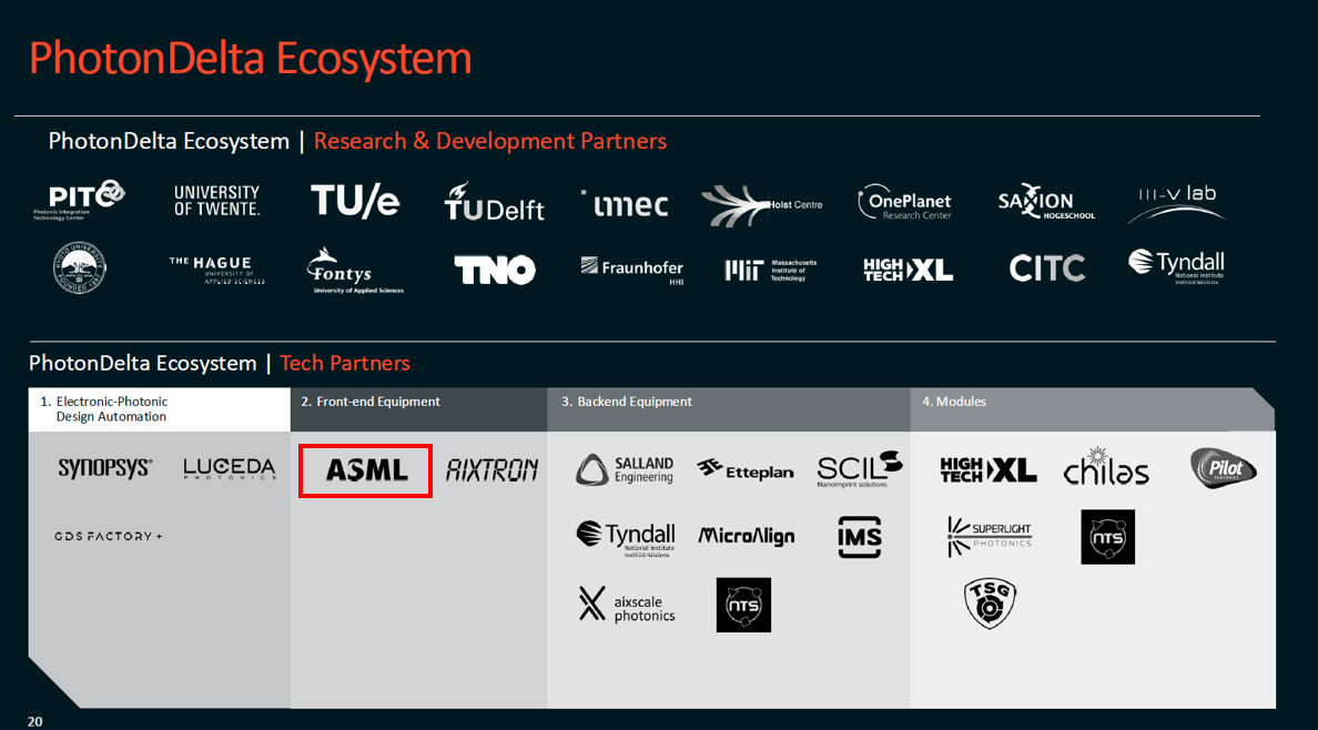
Overview of PhotonDelta Ecosystem. Source: PhotonDelta
The Dutch Integrated Photonics Ecosystem Strengthened Its Presence at SEMICON Taiwan 2025, Partnering with Taiwan and Global Leaders for Deeper Collaboration
SEMICON Taiwan 2025 brought together global leaders from the semiconductor, packaging, and optoelectronics industries. The Dutch photonics community has previously participated in SEMICON Taiwan as aninnovation mission, in 2025 many of the relevant stakeholders visited SEMICON Taiwan again.
The pavilion featured leading companies and research institutes from the Netherlands’ semiconductor and integrated photonics sectors, showcasing the country’s strengths in frontier technologies, ecosystem building, and international collaboration.
The Netherlands’ Strength in Integrated Photonics
The Netherlands has rapidly risen as a global hub for integrated photonics, developing a complete value chain that spans from design to application. Among its industrial champions, SMART Photonics—an InP PIC foundry—has received strategic investments from ASML, NXP, and the Dutch government. With this backing, the company has expanded from 3-inch to 4-inch wafers and scaled capacity from 5,000 wafers per year to 50,000 wafers.
From an international perspective, the Netherlands has built an integrated photonics ecosystem that combines deep technological expertise with commercial scalability. This positions the country not only as Europe’s key photonics hub but also as a strategic global growth center in one of the fastest-expanding segments of the semiconductor industry.
The Netherlands: Latest Technological Advances and Industry Trends in Integrated Photonics
Ecosystem Expansion
Since its inception, PhotonDelta has grown into a network of over 70 partners, covering the entire value chain—from design tools and wafer foundries to packaging equipment, testing platforms, and application-driven companies. This breadth ensures that the Netherlands is not only developing core technologies but also creating an ecosystem capable of scaling commercially.
Diversified Application Fields
Dutch photonics companies are accelerating deployment across multiple application domains, including data centers, high-speed interconnects, LiDAR, medical sensing, and quantum communications. Through hackathons, technology roadmaps, and cross-industry collaborations, innovation is moving at an unprecedented pace, shortening the timeline from concept to commercialization.
Strengthened International Collaboration
PhotonDelta is expanding beyond Europe, forging alliances with the U.S.-based Silicon Catalyst and MIT, and actively engaging with markets in Taiwan and the United States through joint workshops, application testbeds, and pilot deployments. These international connections not only extend the Netherlands’ influence but also ensure global interoperability and adoption of photonic integrated circuits.
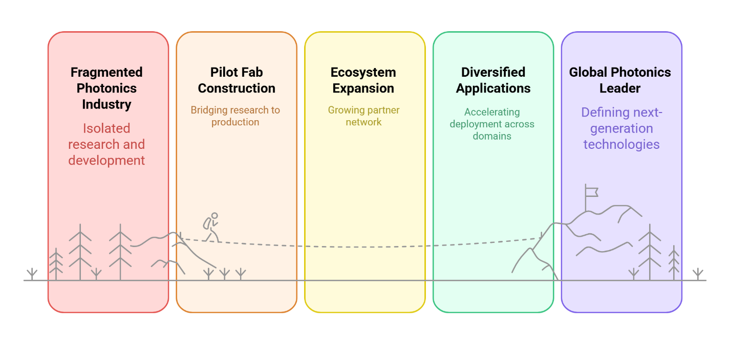
Diagram of Integrated Photons in NL. Source: SemiVision
With its pilot fab capacity, expanding ecosystem, diversified applications, and international partnerships, the Netherlands is positioning itself as a critical global hub for integrated photonics. Much like ASML’s leadership in lithography, this new wave of collaboration and investment could allow the Netherlands to define the trajectory of next-generation AI infrastructure, quantum systems, and optical interconnects.
NL : PIC Summit Europe 2025: Scale and International Visibility
PIC Summit Europe 2025 (November 4–5, Eindhoven) will be the largestIntegrated Photonicsgathering in Europe and an essential platform for driving market adoption. Organized by PhotonDelta, the summit will bring together designers, foundries, packaging integrators, OEMs, investors, and academic experts to discuss how to scale manufacturing, broaden application domains, and strengthen capital and market engagement.
From Lithography Champion to Photonics Pioneer: Building the Next ASML
Strategic Model Replication: Through the EU Chips Act and the Dutch National Growth Fund, the government has allocated over €110 million to support PhotonDelta and establish a national pilot fab for photonic chips. The long-term vision is to build a photonic company on the same scale as ASML, leveraging public-private collaboration and sustained R&D.
Industry Participation: Industrial leaders such as ASML, NXP, and VDL Groep jointly invested €100 million in SMART Photonics, demonstrating horizontal support from equipment to chips and laying the groundwork for a photonics industry model comparable to semiconductors.
Integrated Photonics × Lithography: Combining Dutch Strengths for the Future
Lithography + PICs: The Netherlands’ existing DUV immersion and EUV lithography technologies (led by ASML) are critical for fabricating sub-nanometer photonic devices. Future PIC production may adopt EUV-like high-precision exposure to increase density and integration.
Heterogeneous Integration Challenges: Co-packaging photonic and electronic components on a single chip raises high demands for materials, thermal management, and optical routing, requiring breakthroughs through integrated EDA design and advanced process equipment.
NL Ecosystem Steering Toward 2030: Roadmap and Vision
2030 Ambition: PhotonDelta targets production of 100,000+ photonic wafers per year, creating over €1 billion in annual value.
Global Roadmap Collaboration: The Netherlands contributes to theIPSR-I roadmap, working withMIT and 400+ international organizationsto align global strategies and drive photonic innovation.
Light-Driven Futures: Enabling Key Application Markets
Application Focus: Emphasis is on high-performance computing, data center interconnects, LiDAR, autonomous systems, and medical sensing. Companies like Astrape, Mantispectra, and Delta Diagnostics are already innovating in these fields. Early Achievements: Astrape Networks raised €7.9M in seed funding, signaling a dual momentum of capital and technology in the ecosystem.
Government and Capital: The Twin Engines of the Photonics Revolution
Regional Development: Companies like ASML and NXP support the “Operation Beethoven” initiative, injecting €230 million into Eindhoven’s infrastructure to reinforce its position as an innovation hub.
Connecting the World: The Netherlands as a Global Photonics Hub
International Expansion: PhotonDelta has established an office in Silicon Valley to accelerate US collaboration and signed MoU’s with various partners in Taiwan and Singapore, extending its reach in Asia.
Global Forums: The Netherlands hosts major international conferences such as PIC Summit Europe and ECOC, positioning itself as a focal point for the global photonics community and strengthening international alliances.
This narrative shows how the Netherlands is leveraging its ASML experience to become a world leader in photonic chips, combining government investment, ecosystem collaboration, and long-term technological focus.
NL Industrial Supply Chain and Leading Companies
Public investment and private innovation converge in a national supply chain that covers every stage of photonic-chip development—from materials to systems.

Source: PhotonDelta
Foundries and Platform Developers
SMART Photonics(Eindhoven): Europe’s leading InP foundry offering epitaxy, wafer processing, and backend testing. Its InP platform integrates lasers, modulators, and photodetectors for datacom, quantum communication, and sensing. SMART Photonics is advancing active/passive integration and scaling from 4-inch to 6-inch wafers under the EU pilot-line programme.
Lionix International(Enschede): Lionix develops ultra-low-loss SiN waveguides for telecom and LiDAR. It’s pioneering SiN-on-silicon hybrid process compatibility.
Aluvia Photonics(Twente): specialises in AlOx PICs with erbium-doped waveguide amplifiers (EDWA). Its hybrid AlOx/SiN platform provides compact, low-loss gain elements for AI and HPC interconnects and participates in EU projects on broadband optical amplification.
Together these foundries form Europe’s most diversified photonic-chip manufacturing base—complementary to Taiwan’s strength in silicon photonics and high-volume fabrication.
Packaging and Integration Experts
PHIX Photonics Assembly(Enschede): Europe’s leader in high-precision assembly with sub-micron alignment accuracy. Its 200 mm pilot line covers fiber coupling, die bonding, and automated testing. PHIX works with connector vendors (Senko, US Conec) and Asian OSAT partners to develop standardized “CoWoS-for-Photonics” modules.
Neways(Eindhoven): system integrator linking photonic modules to electronics for telecom, industrial, and medical systems; supports design-for-manufacture and hardware qualification for CPO modules.
Design Tools and Software Providers
Bright Photonics(Eindhoven): develops custom PDKs for SMART Photonics and PhotonDelta members, supports multi-project wafer runs, and provides training through PhotonHub Europe. Its design services standardize layout flows for multiple foundries.
Epiphany(Eindhoven): builds simulation and design-automation tools using digital-twin models that reduce iteration cycles and enable joint design with foundries and packaging partners.
System and Application Leaders
EFFECT Photonics(Eindhoven): develops DWDM transceivers and co-packaged optical engines for AI/HPC data centres; active in EU IPCEI and ORPHEUS projects.
Astrape Networks(Eindhoven): focuses on optical I/O modules for AI accelerators and GPU interconnects targeting terabit bandwidths; secured €7.9 million seed funding in 2024.
PhotonFirst(Almere): specialist in fibre-optic sensing for aerospace and civil engineering and developing embedded sensors for semiconductor equipment monitoring.
Mantispectra(Eindhoven): builds broadband spectrometers for agri-food and biomedical applications and is expanding toward portable AI-based spectral analytics.
From component to system, these companies demonstrate how Dutch innovation translates research into scalable products—an area where Taiwan’s manufacturing capacity and silicon expertise can amplify global impact.
Key Research and Academic Institutions
The Netherlands’ success in integrated photonics rests on its deep academic base and the ability to link research directly to industrial deployment.
TU/e (Eindhoven University of Technology):
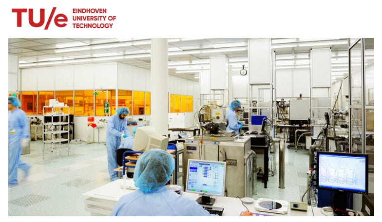
Through theCasimir Institute for Semiconductors and High-Tech Systems, TU/e connects photonics and semiconductor research with industry partners on the High Tech Campus. Its programmes cover InP device physics, SiN process integration, and packaging co-design. TU/e is a founding member of PhotonDelta and partner in Operation Beethoven, expanding cleanroom capacity and talent in Eindhoven’s Brainport region.
Source: TU/e
University of Twente (MESA+ Institute for Nanotechnology):
The MESA+ Institute for Nanotechnology at the University of Twente is one of Europe’s largest research institutes in the field of nanotechnology. It provides state-of-the-art cleanroom facilities, research infrastructure, and expertise that enable the development of micro- and nanoscale devices, photonic components, and advanced materials. MESA+ plays a critical role in supporting both fundamental and applied research, helping translate academic breakthroughs into innovative prototypes and industrial applications. Its research covers areas such as photonic integrated circuits (PICs), quantum devices, sensing technologies, and nanomaterials, thereby strengthening the Netherlands’ scientific foundation in next-generation photonics.
Source: utwente.nl
Technical University of Delft:
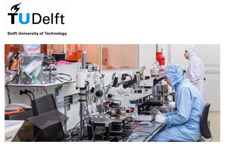
Renowned for micro- and nano-fabrication and optical simulation, TU Delft works with CITC and TNO on thermal design and integration between PICs and electronic substrates and leads EU projects on heterogeneous integration and packaging design.
Source: TUDelft
TNO Holst Centre(Eindhoven):
Applied R&D organisation bridging academia and industry. Its programmes include biophotonic sensing, opto-electronic integration, and high-reliability packaging for PIC modules. TNO co-leads the EU Chips JU-funded 6-inch InP Pilot Foundry, connecting research to pilot-line manufacturing.
PITC (Photonics Integration Technology Centre):
Joint initiative of TNO, TU/e, Twente, and Delft, focused on scaling InP, SiN, and AlOx platforms to industrial production. PITC offers SMEs design-to-fabrication support and standardises process integration across foundries.
CITC (Chip Integration Technology Centre):
Based in Nijmegen, CITC is Europe’s competence centre for heterogeneous integration and advanced packaging. It runs joint training programmes with Eindhoven University and develops 3D integration methods for photonics–electronics co-packaging and thermal management.
NanoLabNLis the Netherlands’ national nanotechnology infrastructure, providing open-access cleanrooms and advanced fabrication facilities that are essential to the country’s leadership in integrated photonics research. With locations in Amsterdam, Delft, Eindhoven, Enschede, and Groningen, NanoLabNL enables universities, research institutes, startups, and industry partners to move seamlessly from fundamental photonics research and prototyping to device fabrication, testing, and small-scale production.
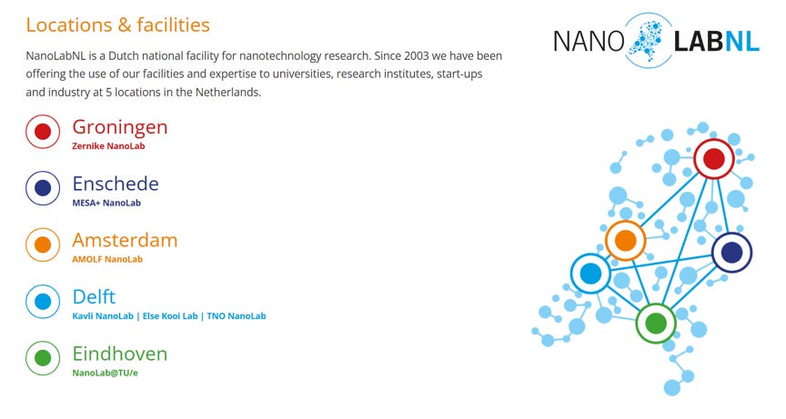
Source: NANOLABNL
New National Facilities and Pilot Lines
TNO 6-inch InP Pilot Foundry:
Funded under the EU Chips Joint Undertaking and PhotonDelta, this facility enables pilot-scale production and standardisation of InP PICs across Europe and offers multi-project wafer access for start-ups and research groups.
Photonic Chip Pilot Line: InP chip fabrication at 6-inch wafer scale
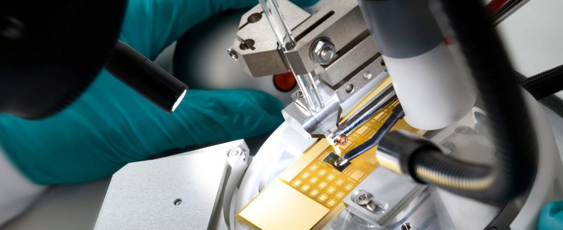
Source: tno.nl
New Origin SiN Foundry:
Dedicated SiN production line supporting low-loss waveguide fabrication and multi-platform integration with InP and AlOx; provides open-access services for R&D and SME prototyping.
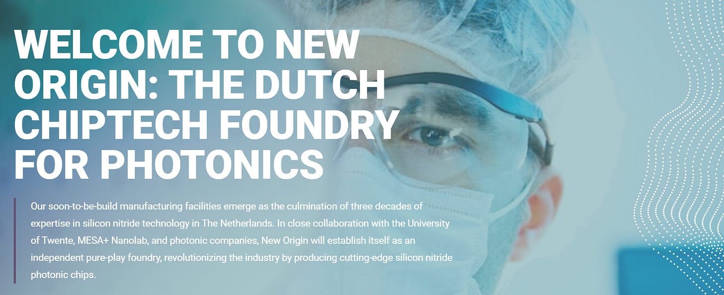
New Origin legt fundament voor wereldwijde revolutie in fotonische chips vanuit Twente
Together these facilities position the Netherlands as one of the few countries with end-to-end capability—from research and design to pilot manufacturing and packaging. Their process compatibility also creates interfaces with Taiwan’s silicon-photonics ecosystem led by ITRI and TSRI, enabling future co-development of heterogeneous integration process flows.
Industry Platforms and Promotion Organizations
PhotonDelta:is the national photonic integrated circuit (PIC) platform of the Netherlands, designed to connect and strengthen the entire European photonics value chain. It brings together research institutions, manufacturers, packaging and testing facilities, and educational organizations into a single, collaborative ecosystem that accelerates the development and commercialization of photonic technologies.
PhotonDelta’s mission is to bridge cutting-edge research with industrial application, ensuring that innovations in photonic integration can rapidly scale into viable products and services. By fostering close cooperation between academia, startups, established companies, and government bodies, it creates a dynamic environment where knowledge, talent, and capital converge.
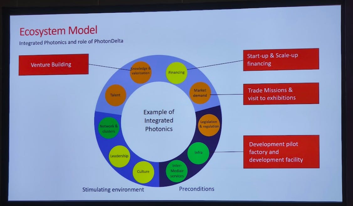
Ecosyetem Model Source: PhotonDelta
At the heart of its activities, PhotonDelta supports:
Research and Development: Driving advancements in integrated photonics, indium phosphide, and heterogeneous integration.
Manufacturing and Packaging: Building capabilities for scalable and cost-effective PIC production and advanced packaging solutions.
Testing and Standardization: Establishing facilities and protocols to ensure high reliability and interoperability of photonic components.
Education and Workforce Development: Training the next generation of specialists to meet growing industry demand.
Backed by substantial government investment and European partnerships, PhotonDelta plays a strategic role in strengthening Europe’s technological sovereignty in semiconductors and photonics. Its efforts extend beyond national borders, actively engaging in international collaboration and ecosystem building to position Europe as a global leader in PIC-based solutions for applications ranging from data communications and quantum technology to healthcare, sensing, and autonomous systems.
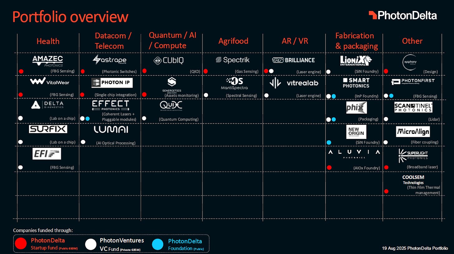
Ecosystem Development in the Netherlands. Source: PhotonDelta
In essence, PhotonDelta is more than just a platform—it is a catalyst for innovation and commercialization, shaping the future of the photonics industry in Europe and beyond.
The Application Frontlines of the Netherlands’ Integrated Photonics Industry: Five Strategic Scenarios in Action
Driven by ASML’s global leadership in lithography, the Netherlands is not only firmly positioned at the core of the world’s semiconductor ecosystem but is also gradually building a world-class integrated photonics industry chain. Under the leadership of PhotonDelta, this transformation goes beyond process and platform development—it extends into application domains, shaping five strategic scenarios with significant market impact. This article highlights these five directions and identifies key Dutch companies actively advancing them, painting a concrete picture of how integrated photonics is taking shape in real-world applications.
AI Training and Inference: Reshaping Infrastructure with Optical I/O and CPO
As AI models scale rapidly, data centers face severe bottlenecks in bandwidth and power consumption with traditional electrical interconnects. This has accelerated the adoption of Optical I/O and Co-Packaged Optics (CPO) as essential technologies for next-generation computing infrastructure. Several Dutch companies are playing a leading role:
SMART Photonics: Europe’s leading InP-based foundry, supplying high-speed modulators and amplifiers—key enablers of optical interconnects such as 200G/400G interfaces.
EFFECT Photonics: Specializes in compact, integrable DWDM optical engines, already collaborating with U.S. module suppliers for intra–data center applications, positioning itself as a potential competitor to Broadcom and Marvell.
PHIX Photonics Assembly: Provides advanced packaging and active alignment services for SiPh and InP modules, serving as a critical player in the realization of co-packaged optical modules.
These companies’ combined strengths in photonic device mass production, optical module integration, and advanced packaging will enable Europe to establish a new optoelectronic infrastructure for AI computing.
Automotive Radar: Highly Integrated FMCW LiDAR Solutions
Frequency-Modulated Continuous-Wave (FMCW) LiDARis regarded as a key sensing technology for fully autonomous driving, requiring photonic platforms withhigh speed, precision, and robustness. Dutch players are already investing significantly:
LioniX International: Developing tunable lasers and optical paths on its SiN platform, with expertise in highly stable FMCW LiDAR transmitter modules in collaboration with automotive supply chains.
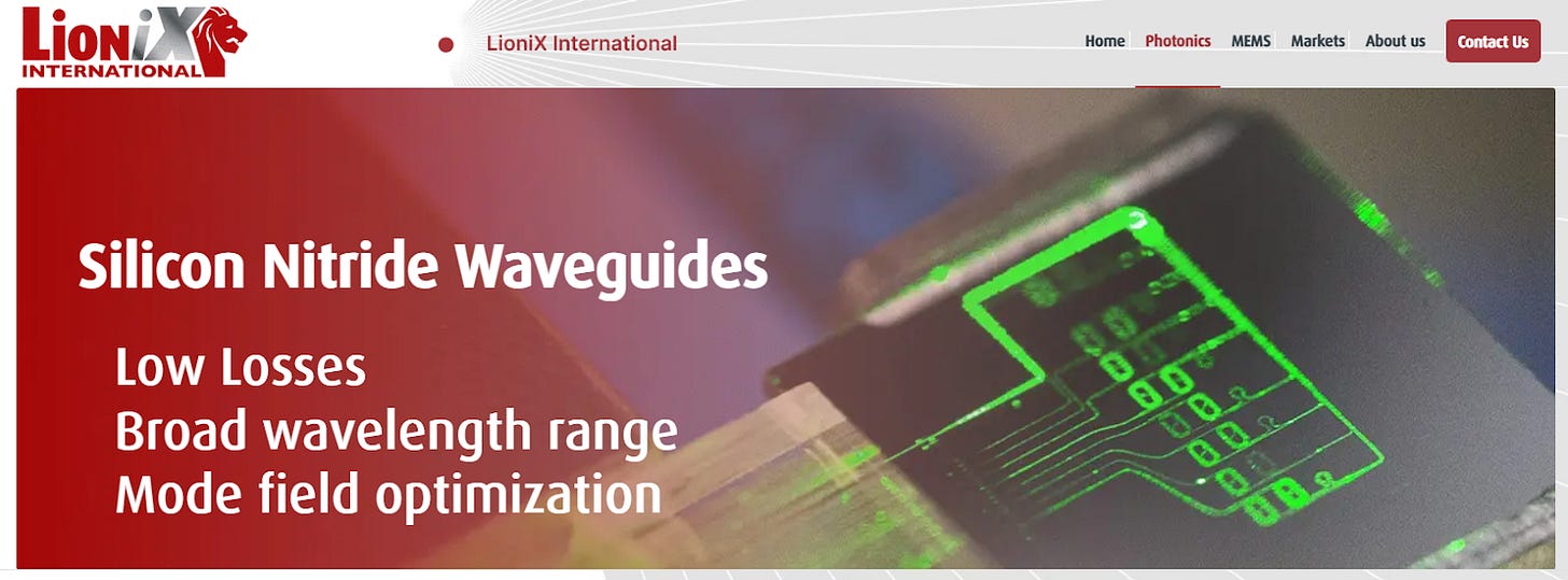
Source: Lionix website
PhotonFirst: Transitioning from optical sensing and pressure measurement into high-density automotive sensing, focusing on module reliability and integration under harsh conditions.
BRIGHT Photonics: A PIC design services provider, helping LiDAR startups optimize optical circuits and modulation architectures, reducing design cycles.
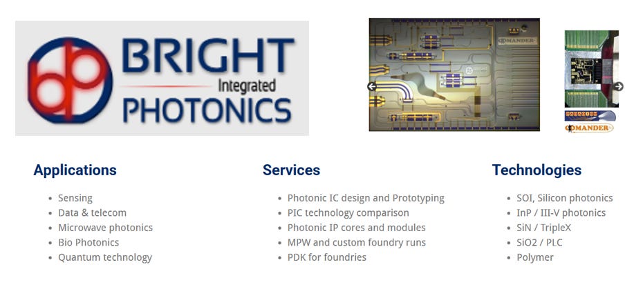
Source: Bright Photonics website
These capabilities allow European automakers to accessintegrated and stable photonic radar solutions, paving the way for integrated photonics in intelligent transportation.
Quantum Communication: Building the Photonic Interconnect Infrastructure
Quantum networks demandultra-low-loss, stable optical pathways and control devices. Integrated photonics, with its CMOS compatibility and scalability, is considered an ideal platform for quantum interconnects. The Netherlands is emerging as a leader in this field:
QuiX Quantum: A globally recognized startup developing photonic quantum processors, headquartered in Enschede, with demonstrated 20×20 interferometer matrices for quantum computing and communication protocol validation.
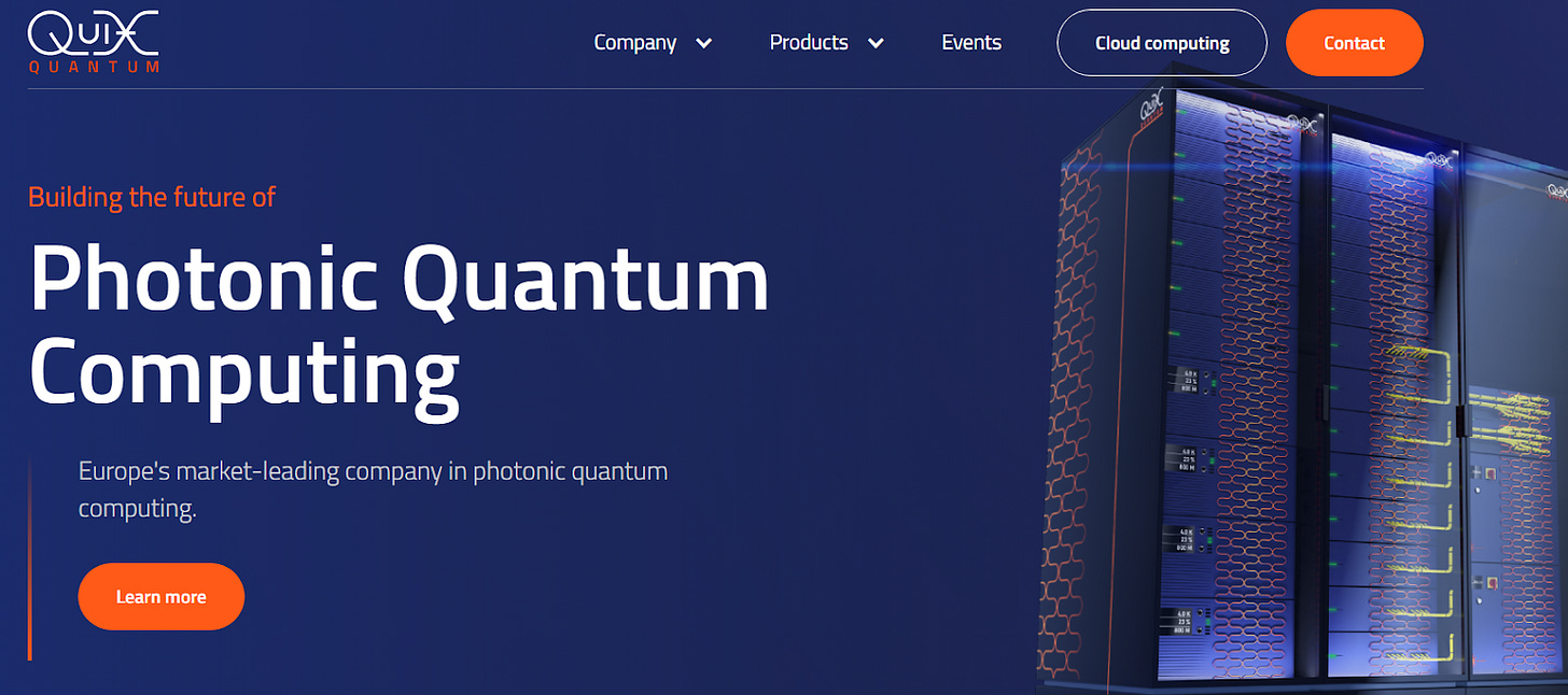
Source: QuiX Quantum website
University of Twente / MESA+ Institute: Known for pioneering quantum photonics research, actively collaborating with global institutes like NIST and CQT on QKD and quantum repeater technologies.
Chilas: Developer of ultra-stable, narrow-linewidth laser sources, providing commercial-grade modules for quantum communication light sources.

Source: Chilas website
These combined efforts reflect how the Netherlands is accelerating the creation of a scalable, practical quantum photonics platform through academic–industrial collaboration.
Biomedical Sensing: Next-Generation Lab-on-Chip Diagnostics
Integrated photonics’ potential for miniaturization, multifunctional integration, and low-cost manufacturing makes it ideal for portable biomedical diagnostic platforms. The Dutch ecosystem has already achieved maturity in this field:
Surfix Diagnostics: Focuses on surface functionalization and photonic biosensor platforms, developing lab-on-chip prototypes for cancer marker and virus detection.
Source: surfixdx.com
Nostics: A startup combining optical detection instruments with AI algorithms, using PIC-based disposable biocards to improve detection sensitivity.

Source: nostics.com
TNO – Holst Centre: Integrates sensor technologies, data analytics, and system design for wearable health monitoring and lab-grade diagnostic applications.

Source: holstcentre.com
High-Speed Switching: Optical Circuit Switches and Integrated Photonics Platforms
As data centers and supercomputers struggle with massive traffic management,all-optical switching (OCS)has reemerged as a promising solution. Dutch research and industry are beginning to take active steps:
LioniX International: Offers reconfigurable photonic circuits capable of building non-blocking switch fabrics.
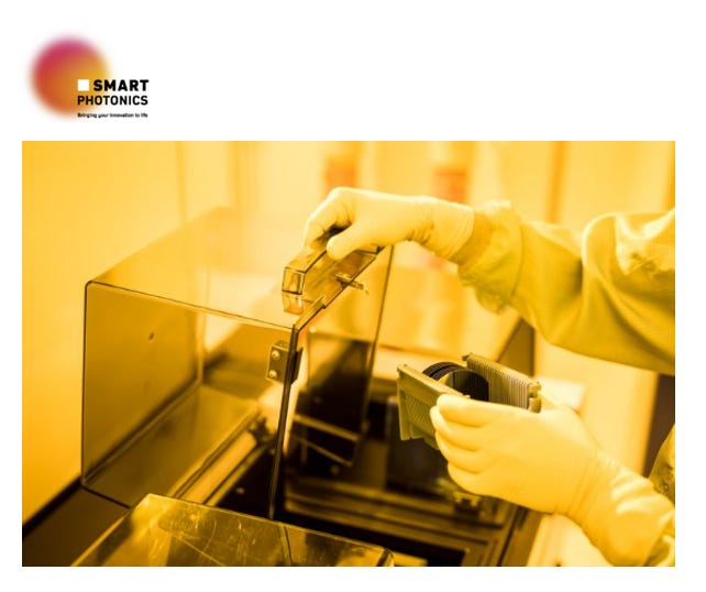
SMART Photonics: Develops tunable lasers and photodetectors for multiplexing and routing modules in high-speed switching architectures.
Source: SMART Photonics
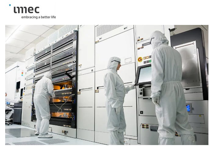
IMEC (Eindhoven branch): Collaborates with TU/e and Holst Centre on prototypes for all-optical switching and reconfigurable optical interconnects.
Source: imec
These technologies promise to reduce data center power consumption while synergizing with AI inference platforms through integrated optical interconnects.
In summary, through these five strategic application frontlines—AI computing, automotive LiDAR, quantum communication, biomedical sensing, and high-speed switching—the Netherlands is translating its integrated photonics R&D into real-world market impact. Supported by PhotonDelta and building on ASML’s legacy, the country is laying the foundation for a globally competitive photonic ecosystem.
Application-Driven Growth: The Expanding Dutch Integrated Photonics Landscape
From data centers to autonomous vehicles, from quantum networks to medical diagnostics, the Dutch integrated photonics ecosystem is steadily evolving from a technology platform orientation toward an application-driven model. This transformation not only reinforces the Netherlands’ role as a strategic hub for European integrated photonics but also creates compelling landing scenarios for international collaboration and capital investment. Looking ahead, the Netherlands is poised to play an increasingly critical role as a “Photonics Capital”, serving as a system integration powerhouse that bridges global semiconductor, AI, and sensing applications into the next technological era.
Source: SemiVision
The Positioning and Strategic Value of PIC Summit Europe
PIC Summit Europe is not just another academic or industry conference; it serves as Europe’s central platform for photonics policy, supply chain collaboration, and market adoption. The event focuses on bridging the notorious “valley of death” — accelerating the transition of photonic integrated circuit (PIC) technologies from laboratory research into commercialization and large-scale deployment. Its strategic value can be understood across four key dimensions:
- Ecosystem Integration
PIC Summit brings together design houses, wafer foundries (e.g., SMART Photonics, AMF), packaging and module manufacturers (e.g., PHIX), materials and equipment providers, as well as system vendors and hyperscalers. By fostering dialogue in a common language, the summit enables the creation of a sustainable pan-European PIC ecosystem. This top-down and bottom-up interaction ensures that Europe can build a resilient and complementary photonics supply chain.
- Policy and Capital Catalyst
The summit often acts as the launchpad for policy announcements and funding allocations, such as the EU Chips Act and the National Growth Fund. This provides participants with direct insights into funding flows and policy priorities, enabling them to align technology roadmaps and market strategies accordingly.
- Technology-to-Application Bridge
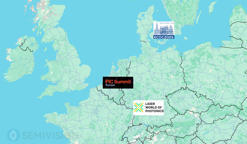
Unlike Laser World of Photonics, which emphasizes technology showcases, or ECOC, which focuses on systems and communications, PIC Summit places special emphasis on application readiness. Covering data center interconnects, quantum networks, automotive LiDAR, biomedical imaging, and sensing, the summit creates dedicated tracks that connect technology providers with end-users, accelerating the formation of viable business models.
- International Collaboration and Visibility
PIC Summit Europe is not limited to European players. For startups and research institutes from Taiwan, Japan, the U.S., Singapore, and beyond, it serves as an entry point into the European market. More than a technical event, it is a hub for global collaboration, investment matchmaking, and ecosystem-building.


2025年8月17日

2025年4月3日

2025年9月16日
Looking Ahead — Launching a New Chapter of Taiwan–Europe Photonics Collaboration at PIC Summit

The year 2025 will mark the beginning of a new phase of structural integration between Taiwan and Europe in the field of Integrated Photonics (PIC / Silicon Photonics). As the global technology landscape rapidly shifts toward AI, high-performance computing, and optical interconnects for data centers, PIC has evolved from a standalone technology into a complete value chain — spanning chip design, packaging, module integration, and system-level applications.
Against this backdrop,PIC Summit Europe 2025 (Eindhoven)will not merely be a technical conference, but a stage for Taiwan to showcase its capabilities and strategic positioning. As both aspeaker and strategic partner, Taiwan will highlight its collaborative potential through four key pillars:
Ecosystem Integration: Linking Taiwan and Europe from Design to System
A complete PIC ecosystem spansdesign/IP, foundry, packaging/integration, testing/validation, and downstream applications. Taiwan holds global leadership in CMOS manufacturing, OSAT, and system integration, while the Netherlands has strong foundations in photonic materials, InP/AlOx platforms, packaging integration, and national platforms such as PhotonDelta and PITC.
At PIC Summit, Taiwan can leverage its strategic partner role to actively participate in“Design & Platform Collaboration Sessions”or startup forums, driving cross-domain connections between policymakers, design houses, and foundry/packaging companies, while engaging key Dutch players likeSMART Photonics, Aluvia, PHIX, and PhotonDelta.
Policy & Capital Catalyst: Driving Industry through National Strategy
High-level forums at thePIC Summitoften intersect with theEU Chips Act, national growth funds, and supply chain resilience initiatives. If Taiwan engages as a strategic partner, it can simultaneously coordinatepolicy alignment, R&D collaboration, and resource mobilizationacross Europe and Asia.
In2024, Taiwan launched theSEMI Silicon Photonics Industry Alliance (SiPhIA), which has now grown to includeover 100 member companies, among them major players such asTSMC,ASE, and other leading foundries, OSATs, and equipment suppliers.
The alliance aims to accelerate Taiwan’s nationalsilicon photonics roadmap, with an eye toward aUS$7.8 billion market opportunity by 2030.
Three Special Interest Groups (SIGs) —System,Packaging & Testing, andEquipment Automation— have already been established to coordinate industrial collaboration and technology development.
Meanwhile,The Netherlands’ PhotonDeltacontinues to serve as one of Europe’s most influential integrated photonics ecosystems, bridging research, industry, and policy to advance next-generation photonic technologies.
Looking ahead,cross-regional collaboration modelsbetween Taiwan and Europe — withHiSPA, TOSIA,andSiPhIAin collaboration withPhotonDelta— are expected to deepen throughjoint pilot-line projects, materials and packaging research, and standardization initiatives, creating a mutually reinforcing innovation corridor across the integrated photonics value chain.
In Taiwan, several key alliances and institutions are actively building a complementary ecosystem:
TOSIA (Taiwan Optoelectronic Semiconductor Industry Association)– An industry association promoting collaboration across the optoelectronic semiconductor value chain.
HiSPA (Heterogeneously Integrated Silicon Photonics Alliance)– Focused on advancing heterogeneous integration between electronics and photonics.
PIDA (Photonics Industry & Technology Development Association)– A major industry organization supporting optoelectronics and photonics development.
SiPhIA (Silicon Photonics Industry Alliance)– A national alliance uniting over 100 companies, driving Taiwan’s silicon photonics roadmap through coordinated industrial development and policy alignment.
ITRI (Industrial Technology Research Institute)– Taiwan’s leading applied research institute, active in PIC technologies and advanced packaging.
TSRI (Taiwan Semiconductor Research Institute)– A national research center supporting advanced semiconductor and photonic integration.
These alliances demonstrate Taiwan’s coordinated national effort to build a silicon-photonics supply chain—from design and wafer processing to packaging and testing—supported by its semiconductor leaders such as TSMC and ASE. Together they provide the manufacturing scale and supply-chain discipline that complement Europe’s R&D-driven photonics ecosystem.
Exchange between PhotonDelta, HiSPA, and TOSIA is focusing on Si with hybrid integration, packaging standardization, and joint development of testing and reliability protocols.
These initiatives link Taiwan’s silicon-photonics and packaging strengths with the Netherlands’ InP ,SiN, and other material technology base, creating a trans-regional supply chain for future photonic ICs as well as to accelerate the development of next-generation PIC technologies for AI, data centers, quantum communication, and sensing applications.
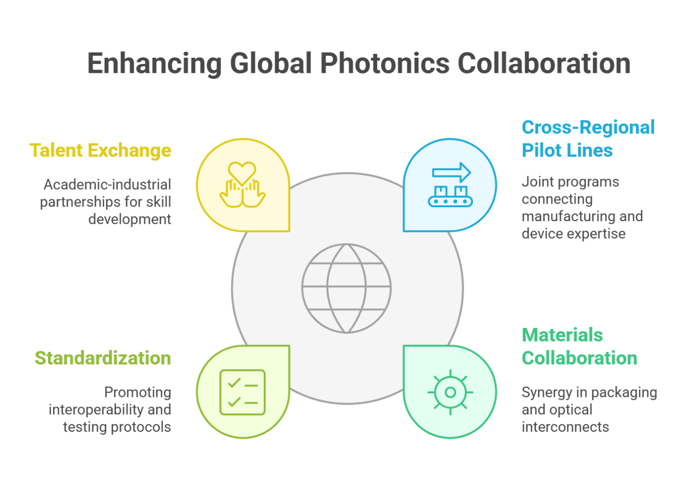
Made by SemiVision
Potential Collaboration Models: Building a Cross-Regional Photonics Partnership
As both Taiwan and the Netherlands accelerate their national photonics initiatives — the two regions are increasingly aligned in vision and capability. Their cooperation could materialize through several complementary models:
Cross-Regional Pilot Lines
Joint pilot-line programs could connect Taiwan’s advanced semiconductor manufacturing and packaging strengths with Europe’s photonic device expertise. Acoordinated InP–Si photonics pilot networkwould enable end-to-end prototyping, from epitaxy and wafer processing to assembly and system validation.
Materials and Packaging Collaboration
Taiwan’s leadership inheterogeneous integration and advanced packaging(Co-Packaged Optics, FO-PLP, and glass substrates) can complement Europe’s specialization inoptical interconnects, micro-transfer printing, and photonic assembly. This synergy may give rise tojoint R&D centersfocusing on reliability testing, thermal management, and hybrid bonding technologies.
Standardization and Ecosystem Alignment
To scale the global photonics market, both ecosystems can jointly promotestandard interfaces, testing protocols, and interoperability frameworksunder international platforms such asIEEE, EPIC, and SEMI. This would enhance supply-chain transparency and reduce barriers for global adoption of photonic integration technologies.
Talent and Knowledge Exchange
Academic–industrial partnerships betweenTU/e, TU Delft, ITRI, and TSRIcould establishjoint fellowship and internship programsto cultivate cross-disciplinary engineers bridging photonics, semiconductors, and packaging.
In essence, aTaiwan–Europe photonics collaboration corridorcould emerge, combining Taiwan’s manufacturing depth with Europe’s innovation leadership. This would not only accelerate the commercialization of next-generation photonic chips but also reinforce global resilience across the semiconductor–photonics value chain.
Technology–Application Bridge: Aligning Research with Market Needs
PIC technology must connect to real applications — AI data centers, optical interconnects, LiDAR, biomedical sensing, and quantum communication — to move beyond the lab.
In dedicated tracks at the Summit, Taiwan can recommend representative application teams to co-present with European technology suppliers, addressingmodule-to-system challengesand solutions:
Data center / AI companiescan share system requirements for high-density optical I/O (power, latency, reliability).
Automotive / LiDAR startupscan present sensing needs and photonic design challenges.
Biomedical photonics teamscan share clinical use cases and measurement specs, accelerating partnerships with European material and detector vendors.
Taiwan and the Netherlands could alsojointly publish a technology white paper or roadmap, outlining their shared vision for PIC in AI, HPC, and sensing applications.
International Collaboration & Visibility: Positioning Taiwan as a Key European Partner
PIC Summit brings together global media, investors, policymakers, and industry leaders. As a strategic partner and featured speaker, Taiwan would gain major visibility through media coverage, international matchmaking, investment opportunities, and network expansion.
For Taiwan — a global leader in semiconductor manufacturing and advanced packaging — engaging with PIC Summit Europe carriesthree layers of strategic significance:
Closing technology gaps in photonic packaging and heterogeneous integration
The Netherlands already hosts leading players like PHIX (packaging & assembly), SMART Photonics (InP foundry), and Aluvia (AlOx amplifiers). Their expertise can directly complement Taiwan’s strengths in silicon wafer manufacturing and system integration.
Understanding Europe’s market and policy direction
Under theEU Chips Act, Europe is channeling billions of euros into photonics pilot lines, manufacturing capacity, and ecosystem building. For Taiwanese companies, insight into these policies and subsidy programs provides a roadmap for future engagement and investment opportunities.
Building transnational collaboration networks
By working with platforms such asPhotonDelta, Taiwan can combine its large-scale wafer fabrication and packaging capabilities with Europe’s leadership inmaterials innovation, optical integration, and ecosystem coordination. Such cooperation not only strengthens Taiwan’s global role but also enables joint leadership in shaping the next-generation AI, HPC, quantum communication, and LiDAR infrastructure.
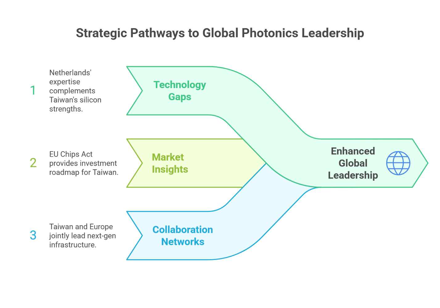
Made by SemiVision
In essence, PIC Summit Europe is more than an industry conference — it is Europe’s strategic engine for scaling photonic technologies from lab to fab, and from niche innovation to global markets. Its positioning at the intersection of technology, policy, and capital makes it an essential touchpoint for countries and companies aiming to remain competitive in the photonics-driven future.
For Taiwan, active participation in PIC Summit Europe could be as pivotal as its early involvement in SEMICON Taiwan or its strategic alignment with TSMC in the rise of EUV lithography. This engagement not only opens the door to European partnerships but also ensures Taiwan’s semiconductor ecosystem remains fully integrated into the global shift toward optical interconnects and heterogeneous photonics integration.


PreviousNext
TopLatestDiscussions








See all