The Infinite AI Compute Loop: HBM Big Three + TSMC × NVIDIA × OpenAI Shaping the Next-Generation Industry Chain
The Infinite AI Compute Loop: HBM Big Three + TSMC × NVIDIA × OpenAI Shaping the Next-Generation Industry Chain
- Source: SemiVision
- Author: SEMIVISION
- Published: 2025-10-13T21:27:39+08:00
- URL: https://tspasemiconductor.substack.com/p/the-infinite-ai-compute-loop-hbm The Infinite AI Compute Loop: HBM Big Three + TSMC × NVIDIA × OpenAI Shaping the Next-Generation Industry Chain


The Infinite AI Compute Loop: HBM Big Three + TSMC × NVIDIA × OpenAI Shaping the Next-Generation Industry Chain
Original Article By SemiVision Research (TSMC, Nvidia, SKHynix, Samsung , Micron , CXMT , Marvell , Broadcom , AWS , GUC , OpenAI )

Oct 13, 2025
∙ Paid

The development of AI has entered an unprecedented acceleration phase. From compute architectures and interconnect technologies to memory bottlenecks, the entire industry is rapidly revolving around a few key companies and technologies. NVIDIA’s recent wave of massive investments has popularized what many in the industry now call the“AI perpetual motion cycle.”In this cycle, AI chips drive compute demand; compute demand stimulates infrastructure investment; and infrastructure, in turn, fuels further expansion of AI chip applications.
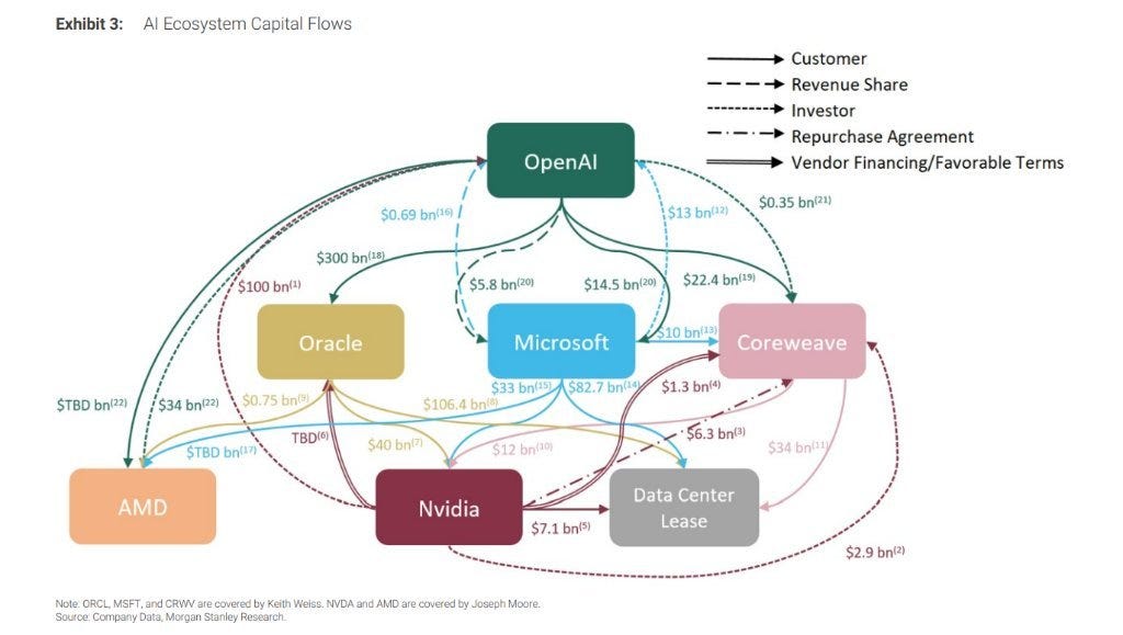
However, at the foundation of this entire cycle liesTSMC’s advanced process and packaging capabilities.
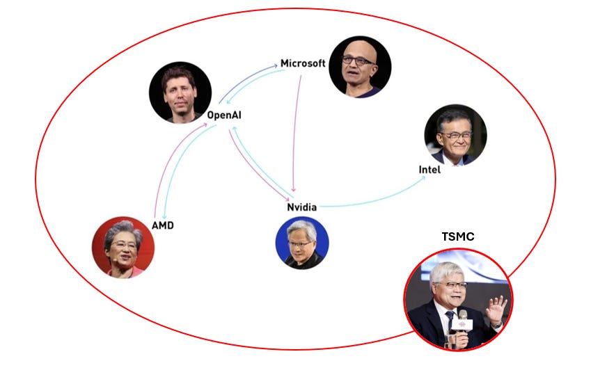
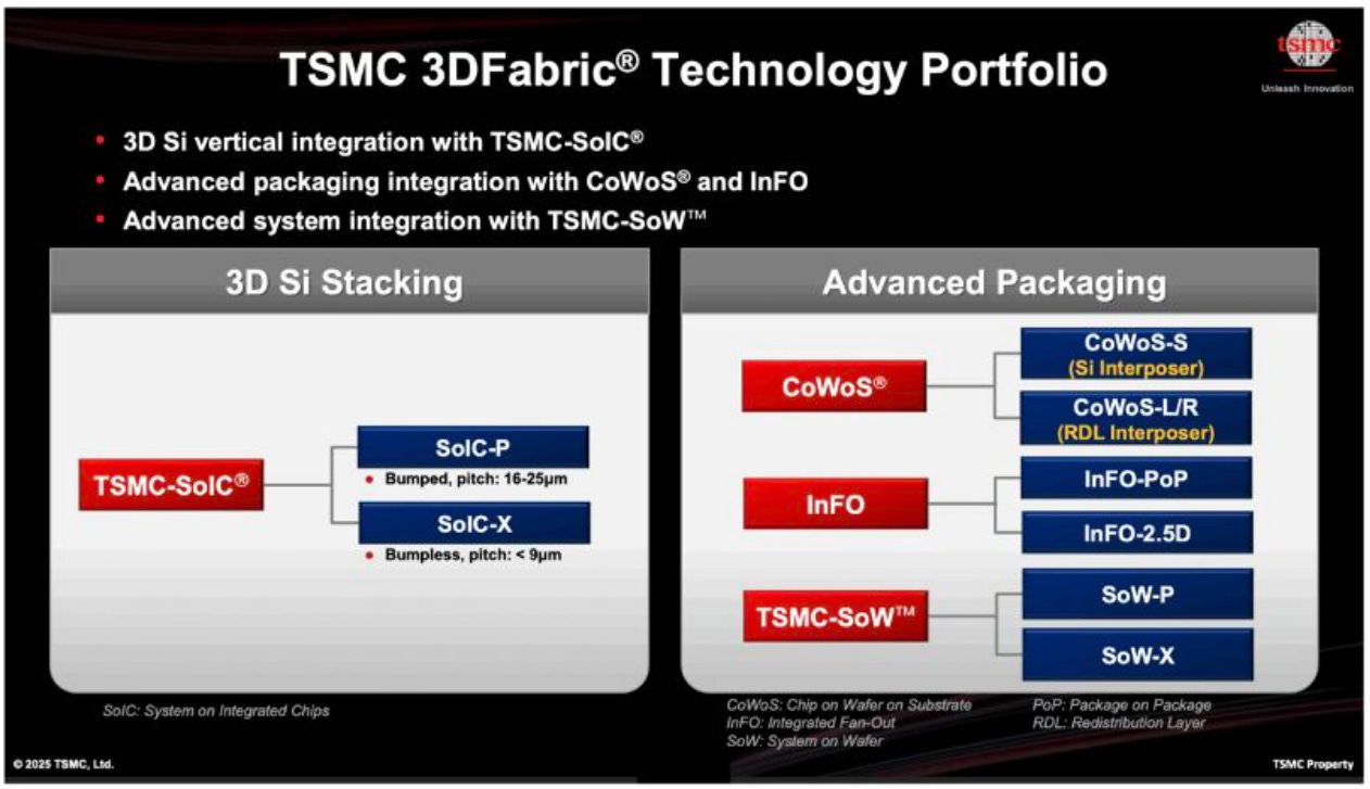
Today, AI chips and high-bandwidth interconnects have fully entered the“advanced process + advanced packaging”era. Whether it’s optical engines, sub-3 nm AI logic nodes, or various advanced packaging technologies such asInFO, CoWoS, SoW, and CoPoS, and even future SiC interposers (CoSoS),TSMC remains the sole strategic hubcapable of supporting the entire stack — from design and manufacturing to packaging and system integration. At the same time, the industry has started using the termCoWoP, where the “P” refers to bothPCBand the broaderplatformconcept, emphasizing the depth and breadth of future system-level integration.
For an AI chip to truly achieve high performance, it’s not just about the process node. It involvesASIC design services, power and signal integrity (PI/SI), and high-speed transmission planning fromRDL copper interconnects to optical engines, all of which drive fundamental changes in data center architecture. NVIDIA’s cluster strategy is evolving fromScale UpandScale OuttowardScale Across, accelerating the adoption ofOptical Circuit Switching (OCS). FromPIC (Photonic Integrated Circuits)toMZI (Mach-Zehnder Interferometer)designs and next-generation transmission materials (e.g.,TFLN, BTO, SOH) supporting speeds beyond 400 G, the entire high-speed optical interconnect ecosystem is being rapidly restructured.
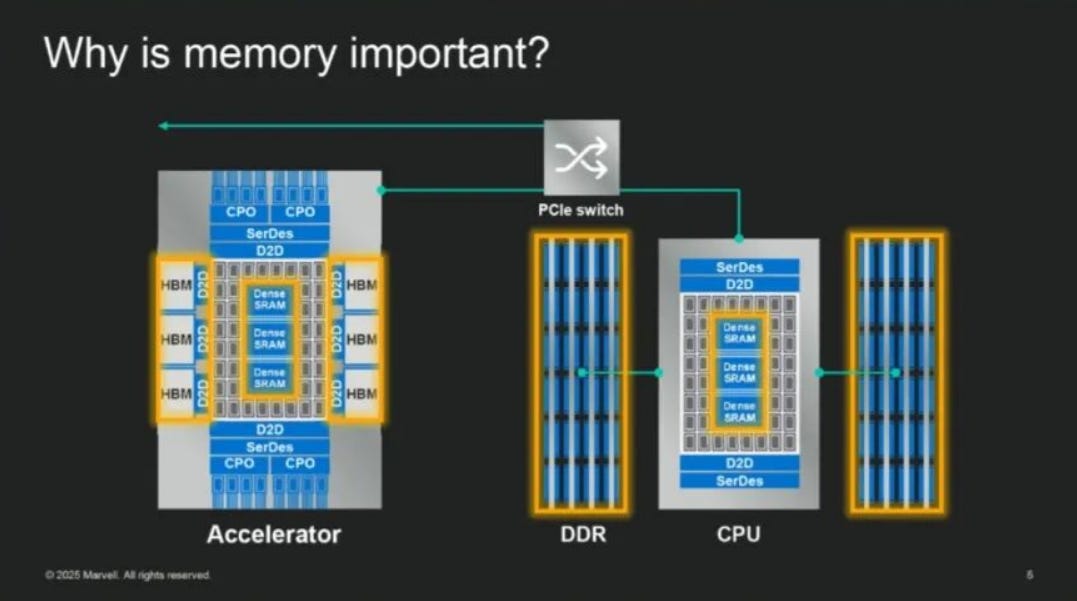
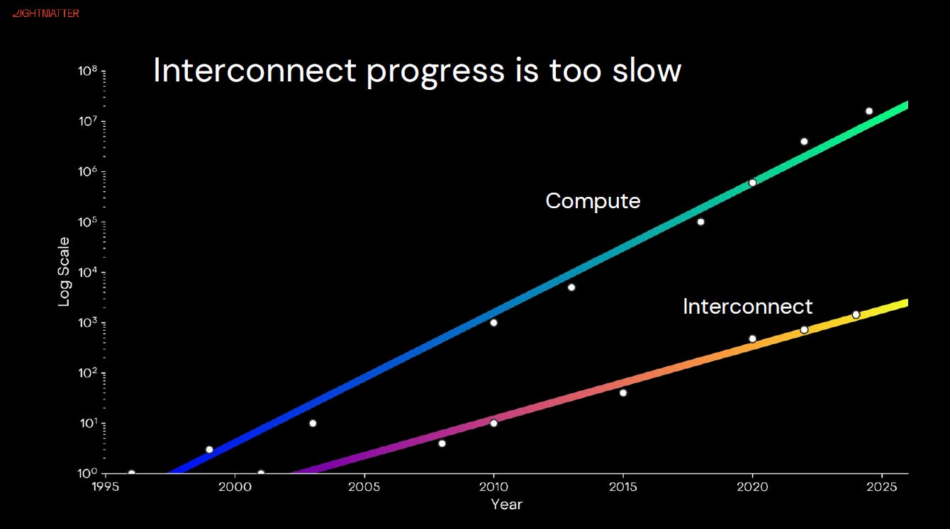
However, the ultimate performance boundary of AI systems is determined not only by compute and interconnect but also bymemory. GPU performance has been advancing far faster thanHBM (High Bandwidth Memory), creating a wideningmemory wallthat has become a central industry focus in 2025.Marvell Technologyhas proposed concrete solutions for memory architectures and optical interconnects atHOT CHIPS 2025andOCP Global Summit 2025, signaling a new wave of innovation to address this critical bottleneck.
The development of HBM goes far beyond memory process technology alone — it represents adeeply coupled engineering systemwith advanced packaging. FromTSV (Through-Silicon Vias)andTCB/HCB/HB bondingto the gradual incorporation of theBase Dieinto TSMC’s process roadmap, HBM has become inseparable from leading-edge integration. This means that in the future AI race, theability to master logic process + memory integration + optoelectronic packaging + interconnect architecturewill be the decisive factor across the value chain. And at the center of all these critical nodes standsTSMC.
This article begins by examining thetechnological pillars behind the “AI perpetual motion machine”, focusing on the evolution of HBM processing technologies, theindustry-wide challenge of the Memory Wall, and the strategic implications ofoptical interconnects and packaging platformsfor future AI architectures.
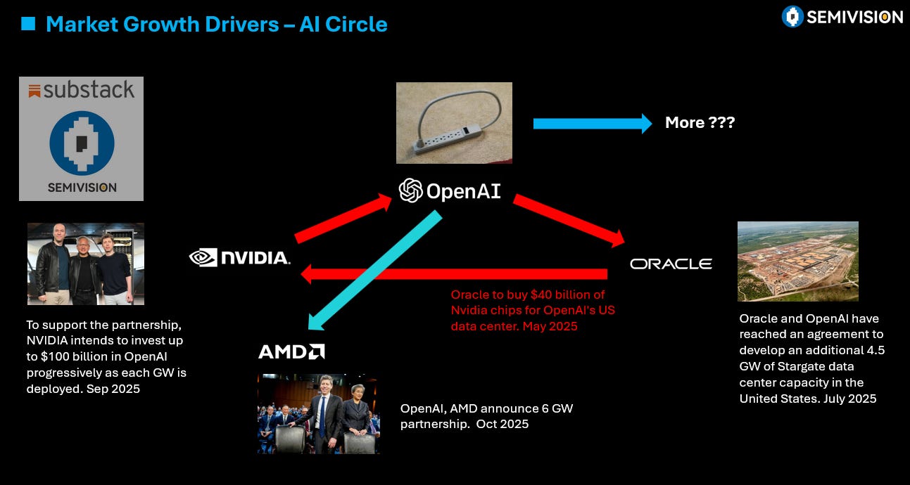
The vast interweaving ofcapital and technological ecosystemsbetweenNVIDIA and OpenAI— spanning hardware supply chains, cloud services, investment strategies, and startup networks — forms a powerfulfinancial enginethat drives the AI boom. Yet behind this flow of capital and compute lies ahidden strategic hub:TSMC.
From NVIDIA’s GPUs to AMD’s compute chips and large-scale cloud server processors, nearly all rely on TSMC’sadvanced process nodes and 3DFabric packaging capabilitiesfor production. In other words, behind every arrow in the capital–technology diagram, thetrue anchor of compute poweris TSMC’s fabs and packaging platforms. Without TSMC, the ongoing AI capital explosion simply wouldn’t exist.
2026 Inflection Point: Systemic Reconstruction of AI Infrastructure
The year2026 will mark a critical inflection pointin the structural transformation of the AI industry. Over the past few years, performance gains in large models have been driven by parameter scaling and GPU cluster expansion. But as compute power transitions fromExatoZetta scale, exponential growth is hittingphysical and engineering limits. The true bottlenecks are no longer GPUs themselves, butmemory bandwidth, packaging interconnects, thermal management, and power supply. Compute is the engine, but bandwidth and thermal management are the drivetrain; when the drivetrain can no longer scale linearly, the entire value chain is redefined.
Energy and Thermal Become Strategic
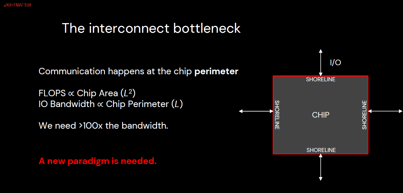
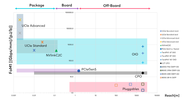
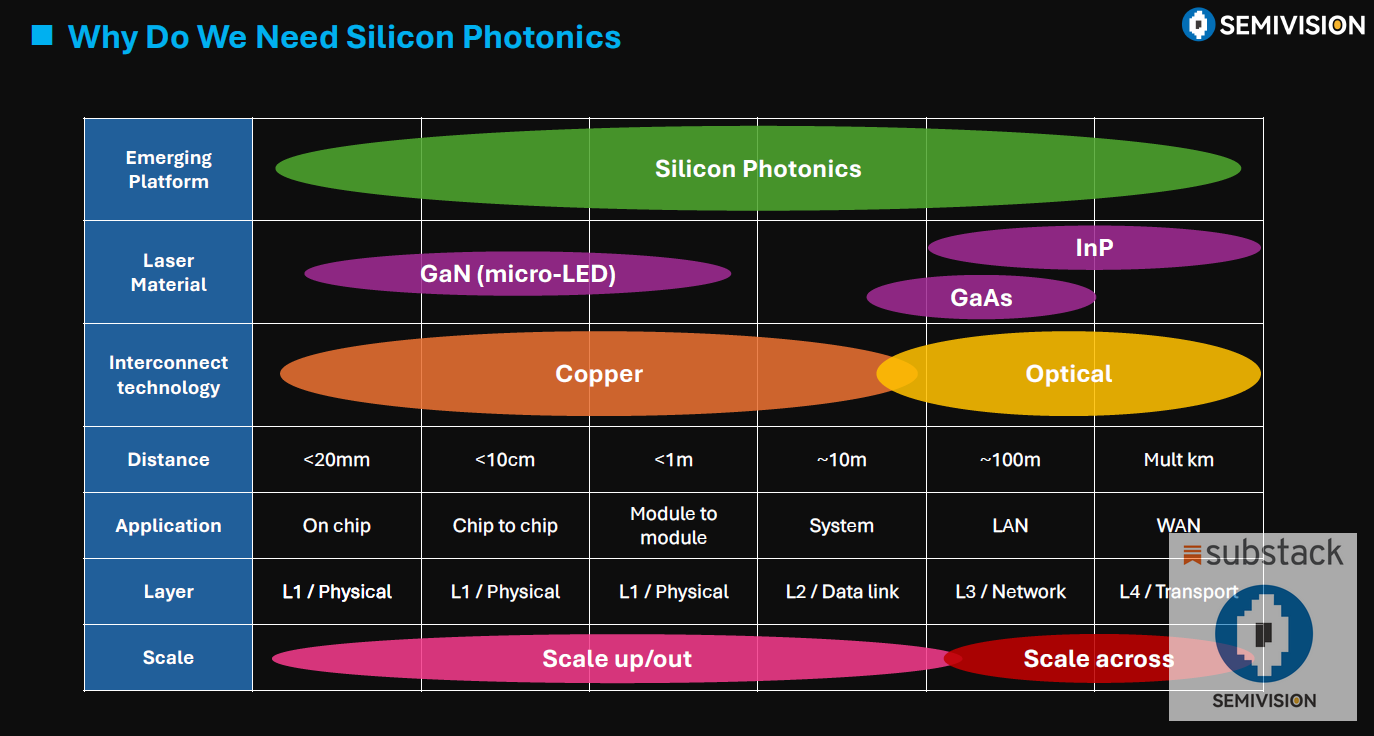
1 GW-class data centersare driving the adoption ofliquid cooling and microfluidic (MCLP)technologies.High-thermal-conductivity diamond materialsare emerging as mainstream heat spreaders. Site selection now depends on bothgrid capacityandwater resources. Meanwhile,electrical interconnects are approaching physical limitsin bandwidth and power efficiency, makingCPO (Co-Packaged Optics)andOIO (Optical I/O)the core of the next architectural shift.
Industry Realignment: From NVIDIA-Centric to Distributed Control
Cloud service providers (CSPs) such asOpenAI, Google, Meta, AWS, and Huaweiare pursuing“de-NVIDIA-ization”strategies—developing their ownASICsand purchasingHBMdirectly. This disperses pricing power and turnsadvanced packaging capacity into a strategic resource. HBM is no longer “just DRAM,” but adeeply integrated system of logic, memory, and interposers.
Thetechnical focus is shifting from stack height to bandwidth engineering. Capabilities inRDL (Redistribution Layer)andPDN (Power Delivery Network)design are becoming key performance bottlenecks. In the short term,CoWoS-Rsupports scaling, whileCoWoS-LandSoICare expected to dominate mass production in the longer term.
Beyond Packaging: CXL and Photonics Reshape Memory Systems
TheCXL (Compute Express Link)architecture is enablingresource poolingandnear-memory compute.CXL 2.0/3.xcombinesSwitching,Pooling, andP2P topologies, usingOS-level hot page migration and remote memory schedulingto increase bandwidth utilization. However, maintaining high performance ultimatelyrequires optical interconnect.
Companies likeAyar Labs, Celestial AI, Lightmatter, and Ranovusare breaking through packaging and reticle limits withsilicon photonics, achievingnanosecond-level latencyandTb/s bandwidth, enablingdistributed memory architectures.HBF/HFMtechnologies serve as thecapacity layer, supplementing memory pools for large-scale inference at lower cost.
The Final Battleground: Packaging Space and System Design
The strategic competition ultimately returns toadvanced packaging and system co-design.Asymmetric HBM placement,multi-layer RDL,PDN partitioning, andoptical module integrationare drivingSTCO (System-Technology Co-Optimization)to become the mainstream design methodology. Companies with strongpackaging integration capabilitieswill command the new value chain.
Marvell and Broadcomare pushingcustom HBM solutionsandin-package optical interconnectsto enter emerging markets.
TSMCis reinforcing its leadership throughHBM base-die technologyandCoWoS/SoICplatforms.
Korean–U.S. alliancesdominate high-end HBM capacity, whileChina faces structural pressure.
2026: The Year of Repricing Bandwidth, Power, and Packaging
By 2026,electricity, water resources, advanced packaging capacity, and optical interconnect capability will all be repriced. The winners will be those who canconvert bandwidth engineering into productivity and pricing leverage. This is not merely a technological race—it is areorganization of power across the supply chain and infrastructure layers.
Risks on the Horizon and Challenges remain:
AI scaling laws may face diminishing returns.
CPO’s thermal management and maintainabilityissues are not yet fully solved.
CXL’s NUMA software overheadcould slow commercialization.
HBF latency limitsits usefulness in training scenarios.
Aswires become antennasandphotons replace copper, the future power structure of AI infrastructure will belong to those who canorchestrate bandwidth, thermal, and energy systems into a coherent whole.
For Paid Members , SemiVision will discuss topics on
The Breakpoint in AI Capability Curves: A Critical Nonlinear Leap by 2026
The Evolution of HBM, HBM IP, and the Memory Wall Challenge
The Concept of HBM IP
TSMC’s Strategic Position in the HBM Base Die Ecosystem
Bandwidth Limits and Packaging Bottlenecks: From DRAM Scaling to RDL Electrical Control
From CoWoS-R Validation to System-Level Packaging Integration
The Memory Wall Problem
Memory Allocation and Expansion under the CXL Architecture
Memory Expansion and Allocation
Solutions Combining Optical Chips and Memory
Celestial AI Photonic Fabric
Lightmatter Passage M1000
Ayar Labs TeraPHY Optical I/O
Ranovus (Odin) Multi-Wavelength Optical Platform
Academic Research: Optical Multi-Stacked HBM
Will HBM Be Replaced by Flash? — The Potential of HBF/HF
SemiVision’s Quick FAQ on HBM & Memory Technologies
Q1: How has HBM evolved across generations, and what are the key features?
Q2: What is HBM IP and why is it needed?
Q3: What is the “Memory Wall” and why does it exist?
Q4: How does CXL address memory allocation challenges?
Q5: How can optical chiplets and photonics help overcome the Memory Wall?
Q6: Will Flash replace HBM in the future?
Technology Advancement for Performance Boost in TSMC’s viewpoints
HBM Allocation and Packaging Space Optimization Strategies
Marvell : SRAM — Boosting Bandwidth and Efficiency in AI/XPU Devices
Marvell: Custom HBM — Tailoring Memory to Match XPU Requirements
Marvell’s Custom HBM Architecture
Marvell : CXL — Expanding and Sharing Memory Through Compute Express Link
Structera A: Near-Memory Accelerator
Integrated Perspective: Marvell’s Memory Strategy
Advantages and Limitations of ASICs in AI Inference
Why are major tech giants investing in custom ASICs?
ASIC WAR : The Race Toward Specialization and Systemization
The Impact of the AI Chip Era on Memory and HBM
Memory Requirements for AI Training and Inference
Large-Scale Clusters and CSP In-House ASIC Development
HBM: The Key Memory Technology Behind Generative AI
- Basic Structure and Advantages of HBM
2.HBM Manufacturing and Competitive Landscape
- HBM Supply-Demand Outlook and Market Size
Why Cloud Service Providers Develop Their Own AI ASICs
ASIC Growth Drives HBM Demand
HBM Competitive Landscape and Supply Chain Evolution
Cerebras :Near-memory computing and HBM alternatives
Summary of Explosive Growth of the HBM Market
Structural vs. Cyclical Cycles — Will AI Reshape the Traditional Memory Boom–Bust Pattern?
HBM4e and Advanced Logic Process Competitiveness — Process Dependence and Strategic Collaboration in Next-Gen Memory
Strategic Collaboration Models Between Foundries and Memory Vendors
Edge AI and Mobile HBM Technology – The Outlook for High-Bandwidth Memory in Smartphones, XR, and Automotive Devices
Breakthrough Conditions: Power, Packaging, and Cost
Strategic Implications for the Edge AI Era
Supply Chain Bottlenecks and Capacity Expansion — Key Factors in HBM / Advanced Memory Manufacturing
Materials and Process Equipment Bottlenecks in Memory Device
Strategies to overcome these bottlenecks
Materials and Process Innovations – Impact of New Technologies on Yield, Cost, and Capacity
5 nm Base Die and Logic Packaging Innovations:
Risk Management and Road-Mapping for New Process Technologies
AI Supercycle and the Restructuring of the HBM Supply Chain
From Nonlinear Capability Leaps to Power Shifts in the Memory Industry
The Breakpoint in AI Capability Curves: A Critical Nonlinear Leap by 2026
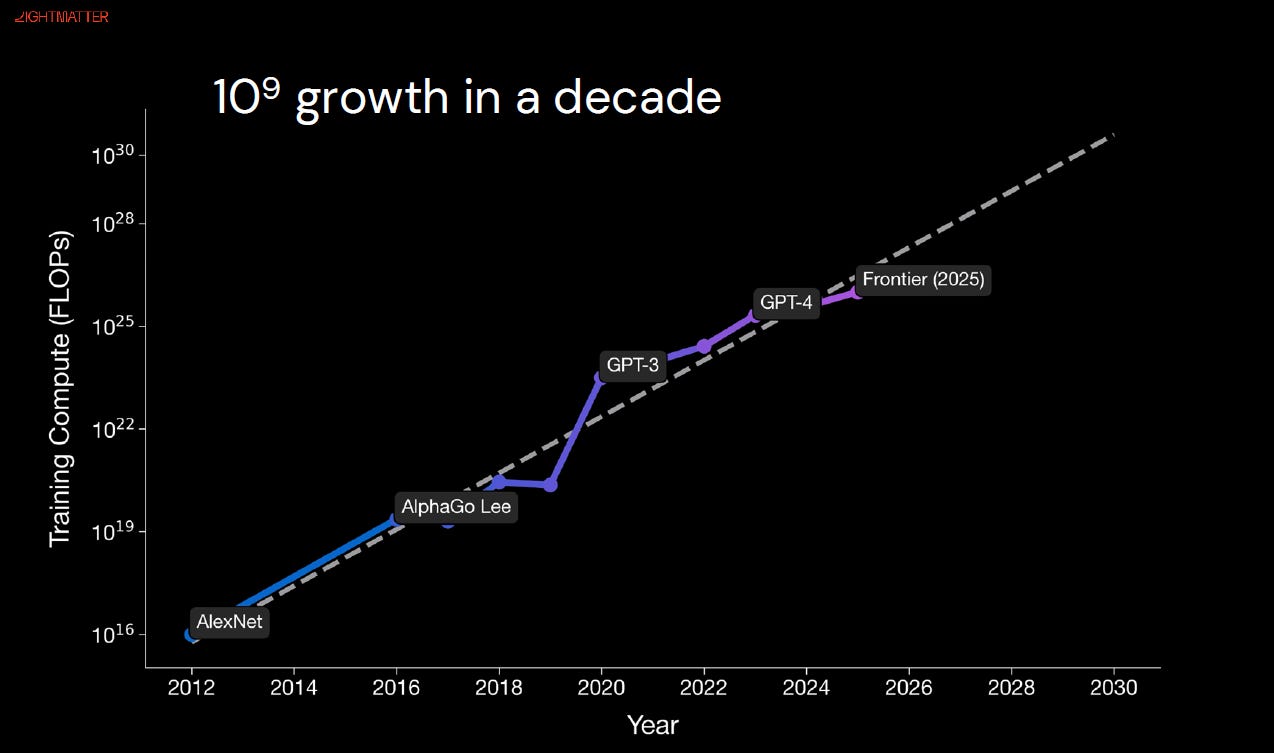
The year 2026 is poised to become a major inflection point in the global AI development trajectory. A compute-driven “capability curve break” is emerging — not merely from scaling models, but from a systemic transformation spanning technology stacks, infrastructure, and capital markets. Looking back, deep learning’s rise in 2012 and the explosion of large language models (LLMs) in 2022 reshaped the entire tech and industrial landscape. Now, with leading model developers expected to increase training compute by roughly 10× by the end of 2025, a concentrated wave of breakthroughs is anticipated in early 2026, acting as a powerful catalyst across the ecosystem.
AI capability growth is not linear. Over the past decade, simultaneous increases in compute, data, and model parameters have followed scaling laws—as model size grows, error rates drop sublinearly. However, once total compute reaches the exaFLOPs–zettaFLOPs range, improvements may shift from a slow curve to step-function leaps. A 1 GW-scale data center can deliver compute equivalent to thousands of supercomputers combined, dramatically boosting language models’ abilities in reasoning chain length, memory, tool use, multimodal integration, and logical coherence. This represents a system-level qualitative leap, not just a quantitative scale-up.
Yet such nonlinear leaps are not guaranteed. The field has long debated the “scaling wall” hypothesis: beyond a certain threshold, performance gains may flatten or stall, entering diminishing returns. Pessimists argue algorithmic and architectural limits will cap model performance, with skyrocketing training costs and energy usage. Optimists counter that synthetic data and transfer learning can sustain training efficiency, while innovations like Mixture-of-Experts (MoE), retrieval-augmented generation, and multi-agent systems can push beyond saturation. In large-scale synthetic data environments, models show no signs of collapse, suggesting the scaling wall may be much farther away than expected.
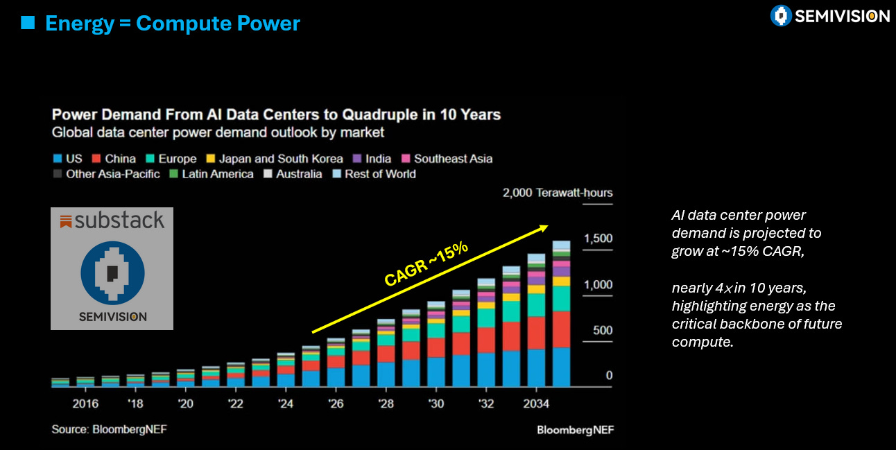
Even if capability curves continue rising, the physical world bottlenecks must be confronted. As 1 GW data centers become standard, energy consumption, cooling, optical interconnect bandwidth, and land infrastructure will pose unprecedented challenges. A single mega training hub could consume as much electricity as a small country. To maintain stable operation, data centers must adopt microchannel liquid cooling, diamond heat spreaders, and direct liquid cold plates. Copper wiring can no longer meet bandwidth demands, making CPO (Co-Packaged Optics) and OIO (Optical I/O) inevitable. Moreover, site selection must shift closer to hydropower or nuclear energy sources to sustain such massive power levels. Infrastructure is no longer just an IT expense — it has become a national strategic asset.

2025年8月29日

2025年10月5日
Market Repricing and Supply Chain Realignment Driven by the Compute Surge
When AI capabilities make theirstep-function leap in 2026, a powerfulmulti-industry, multi-asset market repricing wavewill follow.
First, AI infrastructure suppliers will be direct beneficiaries. Companies providingadvanced cooling, optical interconnects, packaging, and power solutionswill no longer be treated as “backend costs,” but asstrategic nodeson the compute curve.

Second, supply chains will undergo further restructuring. Under geopolitical pressures, theUnited States will strengthen its strategic autonomyin memory, chips, packaging, and energy. Meanwhile,Asia—particularly South Korea and Taiwan—will become indispensable hubs for technology and production capacity.
Third, AI adoption will diverge among end users. Not every enterprise will benefit equally from capability jumps; only those that cantranslate AI efficiency gains into real productivity or pricing powerwill emerge as winners. Thiscapability-to-value conversionwill redraw profit pools across industries.
Fourth,scarce assetswill be repriced.Power infrastructure, critical minerals, water resources, ports, and regulated concessions, due to their non-replicable nature, will see a sharp increase in relative value. At the same time,human experiences, brand trust, and proprietary data, which AI cannot easily replicate, will become central to long-term value reassessment.
Thetechnological rhythm of this transformation is already clear.
Compute architectureswill shift from GPU dominance towardmulti-chip parallelism and the rise of ASICs.
Memory technologieswill evolve fromHBM3E to HBM4E and HBM5.
Data center interconnectswill transition fromPCIe to NVLink and CXL combined with Optical I/O.
Packaging technologieswill advance from traditional2.5D/FCBGAtoCoWoS, SoIC, and fan-out optical packaging.
These shifts will fundamentallyreshape supply chain divisions, elevating the strategic importance ofchip design, advanced packaging, photonic modules, and material suppliers, and creating a new technological and industrial landscape.
It is increasingly evident that2026 will not be a year of gradual, linear growth, but asharp inflection point in the capability curve. As compute power surpasses thezettaFLOPs threshold,technological leaps, infrastructure stress, and capital market repricing will happen simultaneously.
For the industry, this is a moment of“accelerated compression”— faster technology cycles, more intense capital competition, and infrastructure as a critical differentiator. In other words,the future of AI will not just be about model evolution, but about thesynchronous restructuring of the technology–energy–industry–capital–geopolitics chain.
The landscape of theAI chip industry is undergoing a profound transformation. For years, the supply chain — from compute cores (GPUs) to HBM procurement — has beenalmost entirely dominated by NVIDIA, creating a highly concentrated structure. Today, however, technology giants includingOpenAI, Google, Meta, Amazon Web Services (AWS), and Huaweiare strategically pursuing a“de-NVIDIA-fication”approach, developing their own AI chips andreshaping the power dynamics of the HBM supply chain.
HBM (High Bandwidth Memory) is one of thecore components of AI chips, offeringultra-high bandwidth (> 1 TB/s),high stacking (12–24 layers TSV),significant power consumption (20–30 W per stack), andcomplex co-packaging requirements. The market is currently dominated bySK hynix, Samsung, and Micron, with NVIDIA accounting for about70% of total HBM procurement.HBM3 and HBM3Eare the mainstream specifications today, whileHBM4Eis expected to enter commercial deployment in2026.
OpenAI has recentlyshifted its technology strategy, moving away from full reliance on GPUs. It is nowcollaborating with Broadcomto developcustom AI ASICs using TSMC’s 3 nm process, paired withHBM4/HBM4EonCoWoS-L or SoIC platforms. This marks OpenAI’s transition from being anNVIDIA customerto becoming adirect HBM buyer, a shift that represents not just a technical change, but afundamental redistribution of power within the supply chain.
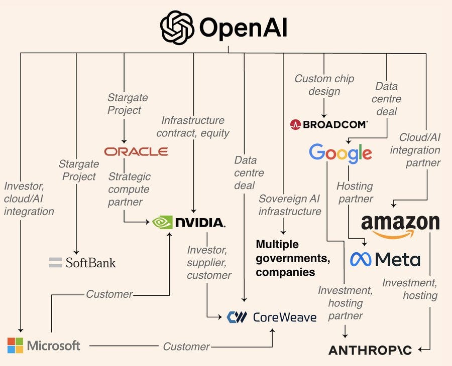
OpenAI CEOSam Altman recently traveled to South Korea, signingHBM supply LOIswith Samsung Chairman Jay Y. Lee and SK Group Chairman Chey Tae-won, with aplanned procurement volume of 900,000 DRAM wafers per month—equivalent toroughly 75% of the combined capacityof Korea’s two major memory suppliers. This move indicates OpenAI’s intention toprocure directly from memory manufacturersrather than through NVIDIA, signaling an erosion of NVIDIA’s dominance over the HBM market.
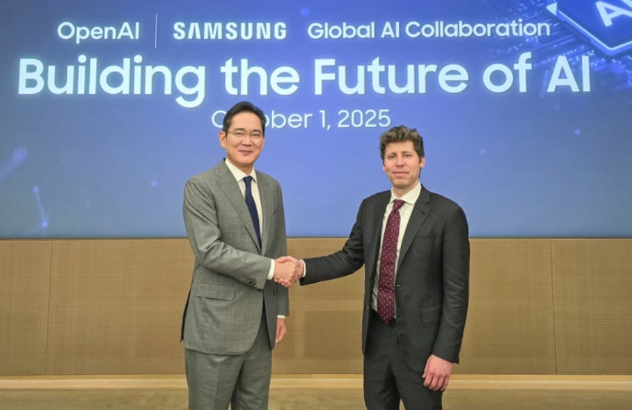
Samsung and SK join OpenAI’s Stargate initiative to advance global AI infrastructure
Historically, NVIDIA hassecured strong pricing leveragethrough long-term pre-purchases, driving down unit HBM prices. In the future, asOpenAI, Google, AWS, Meta, and Huaweienter direct negotiations,three major shiftsin HBM pricing and capacity allocation are expected:
Bargaining power will decentralize, reducing memory vendors’ reliance on a single customer.
ASP (Average Selling Price)is expected to rise significantly, especially forHBM4E and HBM5product lines, which will undergo a pricing revaluation.
Advanced packaging capacitywill quickly be locked up. Major OSATs likeTSMC, Amkor, ASE, and SPILwill become critical strategic nodes in this new competitive landscape. Upstream packaging and testing resources will turn intokey strategic assetsfiercely contested by cloud giants.
HBM’s technical evolution is also drivingparallel advancements in packaging and thermal management.CoWoS, SoIC, and H-Cubetechnologies will see wider adoption, whilethe high power dissipation of HBMwill pushmicrochannel liquid coolinganddiamond heat spreadersinto the mainstream. At the same time,CPO (Co-Packaged Optics)andOIO (Optical I/O)will become essential solutions to bandwidth bottlenecks. In this tightly coupled compute–memory architecture,power and thermal design are no longer secondary engineering details—they are thedeterminants of commercial viability, and a new battleground for OSATs and materials companies.
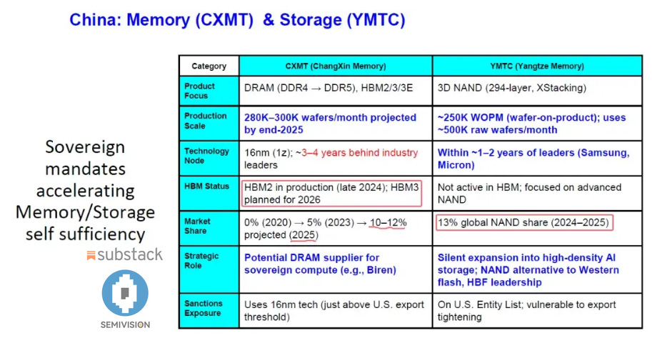
For the past five years, the AI chip market has been built on theGPU-driven NVIDIA economy. The next five years will mark amulti-chip, multi-architecture, multi-supply-chain era, wherecompetition and collaboration coexist. OpenAI’s in-house ASIC strategy is directly reshaping the HBM landscape.Samsung and SK hynix, with their capacity and technical strengths, are emerging asnew pricing power centers;TSMC and OSATswill dominatepackaging and system integration; andNVIDIA’s supply chain leverage will gradually diminish.
2026 will not only be the year of AI capability leaps—it will also mark thebeginning of synchronized restructuring across memory, packaging, energy, and industrial power structures, redefining the entireAI value chain.
The Evolution of HBM, HBM IP, and the Memory Wall Challenge
- The Development History of HBM
Origins and Fundamentals of HBM
High-Bandwidth Memory (HBM)is a stacked DRAM technology designed to deliverextremely high memory bandwidth, far surpassing that of traditional GDDR or DDR memory. Conventional memory improves bandwidth by increasing clock frequency or bus width, but these approaches are constrained by power consumption and signal integrity issues.
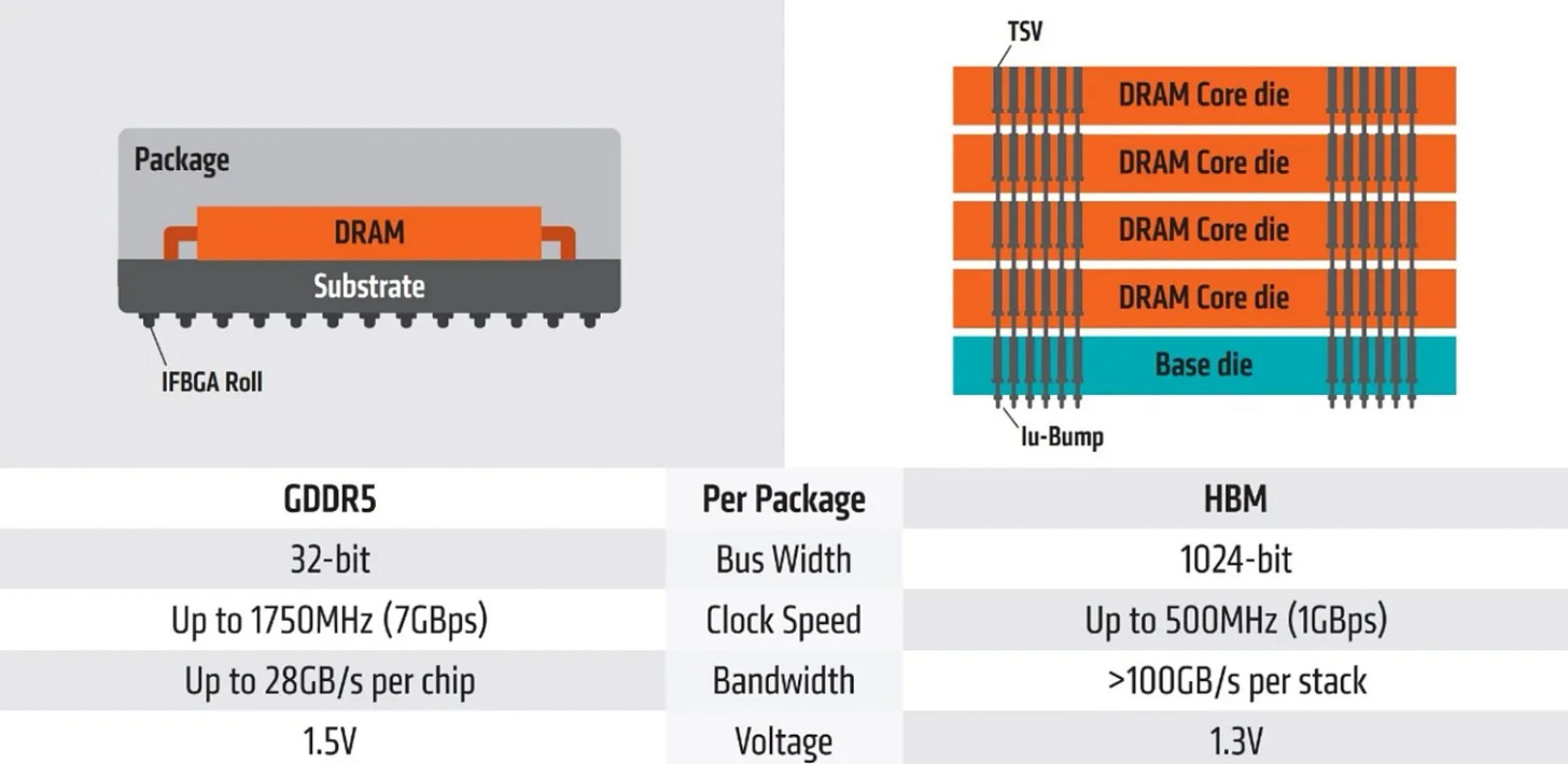
HBM adopts a3D-stacked architecture: multiple DRAM dies are vertically stacked on top of a base logic die and interconnected usingthousands of Through-Silicon Vias (TSVs)andmicro-bumps. This stacked memory module is then connected to the processor via asilicon interposer(2.5D integration).
Thisvertical stacking enables thousands of I/O connections per HBM stack, providing bandwidth in the range ofhundreds of GB/s up to more than 1 TB/s per stack. Because of the extremely dense interconnects, HBM must be placed in close proximity to the compute die, typically within aCoWoS or SoIC advanced packaging platform. Although HBM comes with higher manufacturing complexity and cost, itsignificantly reduces power consumption and footprintcompared to traditional memory architectures.
Evolution of HBM Generations
The table below summarizes thestandards, bandwidth, and key features of each HBM generation.
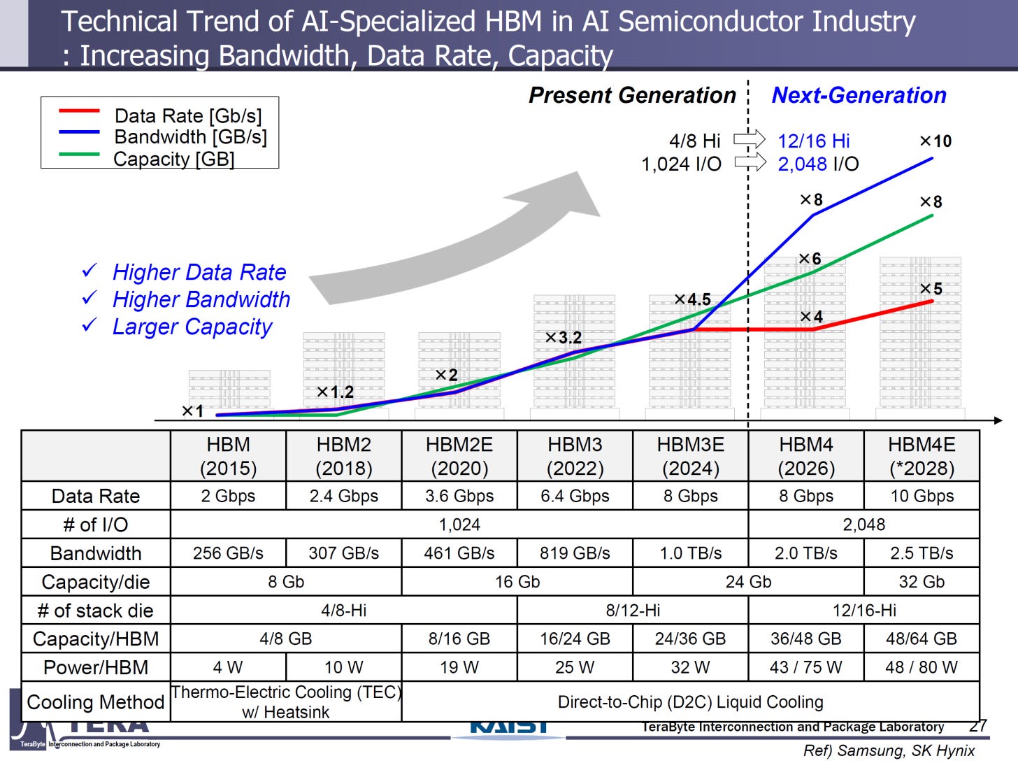
In2013, JEDEC released thefirst-generation HBM (JESD235), marking the beginning of standardized high-bandwidth stacked memory.
Each subsequent generation hasincreased bandwidth,expanded the number of channels, andraised stack heightto support more capacity.
Starting withHBM2, pseudo-channel architecture was introduced to improve efficiency.
HBM4represents a major leap,doubling the number of channels to 32,lowering core voltage to 1.05 V, and addingDirected Refresh Management (DRFM),WSO bus remapping, anddecision feedback equalization— enabling higher data rates and improved signal reliability for next-generation AI and HPC systems.
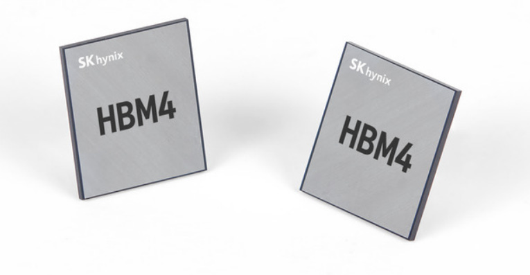
SK hynix completed the world’s first HBM4 development in 2025 and is preparing for mass production. Looking ahead, HBM5/6 may adopt glass substrates and immersion cooling technologies.
SK hynix Completes World’s First HBM4 Development and Readies Mass Production
The future HBM roadmap shows four generations from HBM5 to HBM8 beyond 2029. Research from KAIST indicates that HBM5 could achieve bandwidths of up to 64 TB/s with 16-high stacking. HBM6/7/8 are expected to incorporate copper-to-copper bump-less hybrid bonding and double-sided interposers. HBM8 may even be integrated withHigh-Bandwidth Flash (HBF), leveraging 3D NAND stacking to provide over 1 TB of capacity.
The Concept of HBM IP
HBM IP refers to the silicon intellectual property of HBM controllers and PHY circuits that can be adopted by SoC designers. This type of IP enables chip companies to quickly integrate HBM with AI accelerators or data center SoCs without developing the HBM interface in-house. Two examples illustrate this:
Synopsys HBM IP– Synopsys provides a complete set of HBM controller, PHY, and verification IP. Its 6th-generation HBM4 IP achieves 12 Gb/s per pin and over 3 TB/s total interface bandwidth, with robust design verification and support inherited from previous generations.

Global Unichip (GUC) HBM IP– GUC’s HBM4 IP supports 12 Gbps/pin speeds, using proprietary interposer routing to reduce signal loss and power consumption, while integrating I/O monitoring within the controller to enhance reliability. The company has already taped out multiple 8.4/8.6 Gbps HBM3E products for data center customers.

A key signal emerged at TSMC’s recent Tech Forum: TSMC is officially entering the design and manufacturing of HBM base dies, collaborating deeply with the three major DRAM vendors — Samsung, SK hynix, and Micron. This marks a strategic shift: HBM is no longer merely a DRAM process competition, but has entered a new era ofmemory–logic co-design and integration.
Currently, there are two main approaches to increasing HBM bandwidth. The first iscontinued DRAM process scaling, which boosts the data transfer rate of each individual chip. The second isincreasing the number of stacked layers (Hi stacks)to expand total bandwidth. However, as signal transmission speeds approach their physical limits,Power Integrity (PI)andSignal Integrity (SI)at the packaging level have become critical factors for maintaining system stability. To simultaneously achieve high speed and stable operation, thedesign of the Redistribution Layer (RDL)has become the architectural centerpiece.
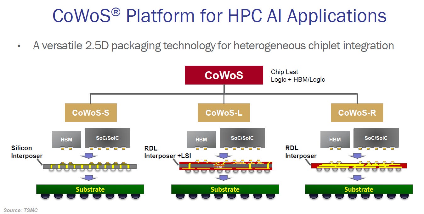
To ensure signal integrity and power stability in high-speed packaging, the number of RDL layers must be continuously increased, creating more sophisticated ground shielding and power distribution networks. This is whyTSMC’s CoWoS-R platformhas become a crucial testbed for HBM packaging verification. CoWoS-R utilizes an organic interposer combined with multilayer RDL structures, enabling full-scale electrical, thermal, and mechanical validation under realistic large-area, high-density conditions.
In other words, TSMC is redefining the technological foundation of HBM through itsco-optimization of advanced packaging and process technologies. The focus has shifted from simply scaling DRAM stack height and bandwidth toward an era of“System Bandwidth Engineering,”whereelectrical design at the packaging levelplays the central role in sustaining future performance scaling.
TSMC’s Strategic Position in the HBM Base Die Ecosystem
As HBM4 and HBM3e enter the ultra-high-bandwidth era, the focus of memory design has shifted from DRAM stacking and process scaling toward“co-integration of memory and logic.”In this transformation,TSMC plays a pivotal role as both a foundry and advanced packaging platformwithin the HBM ecosystem. At its Technology Forum and OIP (Open Innovation Platform) events, TSMC clearly stated that it will collaborate with the three major DRAM vendors —Samsung, SK hynix, and Micron— to co-develop the next generation of HBM base dies.

Thisbase die (logic die), located at the bottom of the HBM stack, is no longer just a simple control or test logic chip. It is evolving into ahigh-performance logic layerthat integrateshigh-density I/O PHY, clock management, error correction (ECC), and power control circuits. Because these functions require advanced logic processes, DRAM vendors are increasingly relying on external foundries for manufacturing. According to TrendForce, starting with HBM4, the base die will move to FinFET nodes, and for HBM4e may even adopt 3nm-class technologies. TSMC has therefore introduced atwo-tier foundry strategy: using12FFC+ (12nm class)for mainstream products, andN5 (5nm class)for top-tier HBM4 customers, providing flexibility between performance and cost.

This tiered process strategy positions TSMC not merely as a manufacturing provider but as aco-architect of the overall HBM packaging structure. By working closely with DRAM vendors onbase die design, signal routing, and packaging validation, TSMC is effectively transforming HBM from a traditional memory component into aheterogeneous stacked device with integrated logic functionality. This integration is essential for HBM to continue advancing towardhigher bandwidth and lower power consumptionin the coming generations.
Bandwidth Limits and Packaging Bottlenecks: From DRAM Scaling to RDL Electrical Control
To increase HBM bandwidth, there are currently two main approaches:
Enhancing DRAM process scaling, such as shrinking cell capacitors and bitline dimensions or increasing I/O operating frequencies.
Increasing the number of stacked layers (Hi count)to boost overall data parallelism through denser TSV vertical channels.
While both methods can improve bandwidth, each faces fundamental physical and engineering limits.
As DRAM processes shrink to the 1b/1c nm nodes, resistance and capacitance effects become more pronounced, making signal delay and noise control increasingly difficult. Meanwhile, as stack heights reach 12-Hi and even 16-Hi, TSV channels lengthen, impedance rises, and coupling interference and thermal density issues worsen. As a result, even if DRAM device performance improves, theoverall bandwidth is constrainedif signal integrity (SI) and power integrity (PI) cannot be maintained within the package.
This is whyTSMC and its memory partners are now focusing on packaging-level challenges — specifically, the electrical and structural design of the Redistribution Layer (RDL). The RDL connects the base die, DRAM dies, and SoC, acting as the “vascular system” for high-speed data channels. To maintain stable transmission at >10 Gbps per pin, the RDL must addressimpedance matching, crosstalk suppression, power noise management, and thermo-mechanical stress controlsimultaneously.

To achieve this, TSMC’sCoWoS-R architectureemploysGSGSG (Ground-Signal-Ground-Signal-Ground) routingand multilayer shielding structures within the RDL. Inner ground shields and dielectric isolation layers suppress high-frequency crosstalk and EMI, whilediscrete decoupling capacitorsare integrated near the C4 bumps to stabilize power delivery, reduce IR drop, and minimize noise coupling. Because HBM’s signal paths are extremely short,even minor impedance discontinuities can shrink eye diagrams or increase BER, making precise control overRDL geometry, dielectric thickness, and copper trace distributionessential.
As signal channel counts increase, more RDL layers are required, which introduces new manufacturing challenges:layer-to-layer alignment must be controlled at the micron scale, and CTE mismatches in dielectric materials can cause warpage or layer slippage. TSMC addresses these issues in CoWoS-R by using anorganic interposer, whose material elasticity helps absorb stress and reduce deformation mismatch between silicon and substrate, ensuring long-term reliability and stable transmission.
In short, among the multiple bottlenecks in scaling HBM bandwidth,the PI/SI performance of the RDL has become the critical support point—the decisive factor determining whether a packaging architecture can pass high-speed verification.
From CoWoS-R Validation to System-Level Packaging Integration
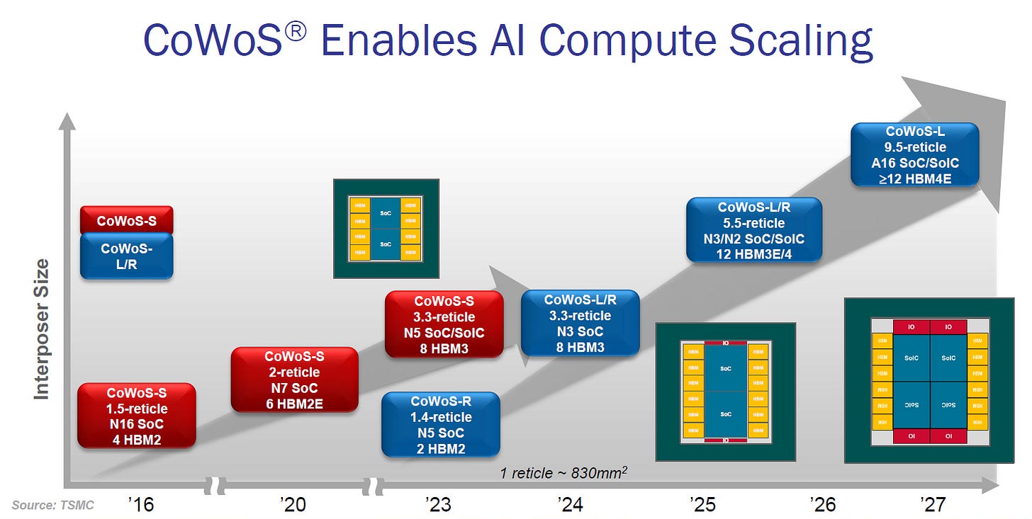
To validate the complex RDL designs and electrical stability described above,TSMC and its customers widely use CoWoS-R (Chip on Wafer on Substrate – RDL Interposer)as theirtechnology verification platform. Unlike traditional TSV silicon interposers, CoWoS-R usesorganic interposers combined with RDL routing, offering higher manufacturing yield and faster design iterations. Engineering teams can use this platform tosimulate full signal routing between multiple HBM dies and large SoCs, performing comprehensive tests such aseye diagrams, insertion loss, crosstalk, IR drop, and power noise, allowing fine-tuning of line width, spacing, layer count, and decoupling capacitor placement.
TSMC’s CoWoS-R currently supportsminimum 4 μm pitch (2 μm line/space)RDL layouts, maintaining strong electrical performance in ultra-dense environments. This makes CoWoS-R the“mid-stage validation platform” for HBM packaging: before entering mass production withCoWoS-LorCoWoS-S, electrical and mechanical fine-tuning is carried out at this stage to reduce production risk.
Theend-to-end design flow— from base die to final packaging — requiresmulti-layered optimization:
Base Die I/O and PHYmust be co-designed with the package routing to shorten signal paths and reduce latency.
RDL routing and shielding strategiesmust balance signal frequency, crosstalk, and power noise.
C4 bump arrays and underfill material selectiondirectly impact die-to-die alignment precision and mechanical strength.
Additional considerations includethermal management(e.g., thermal vias or micro-cold plate structures near high-power regions) andclock tree jitter controlto ensure system synchronization.
After these design steps, engineering teams use the CoWoS-R platform forSI/PI simulation and real measurements, iteratively adjusting RDL routing, shielding layers, and decap placement based on the results. This process not only verifies the stability of high-speed channels but also establishes CoWoS-R as acritical validation stage for next-generation HBM packaging.
Ultimately, through this“design–package–test” closed-loop flow, TSMC is advancing its advanced packaging platform towardSystem Technology Co-Optimization (STCO), laying thehigh-bandwidth, low-power, and scalable foundationfor the HBM and AI accelerator era.
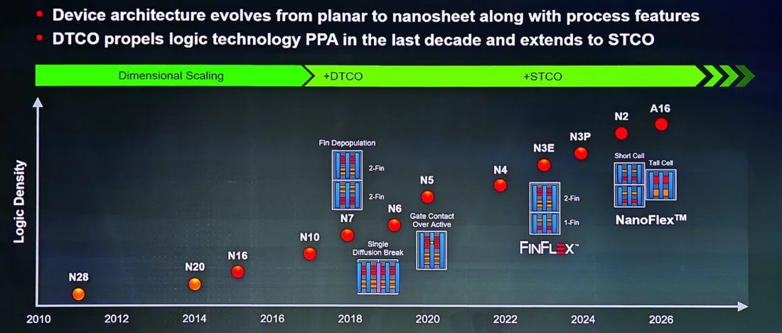
The growing adoption ofHBM IPfurther enables widespread integration of HBM into AI GPUs, data center SoCs, and high-performance computing ASICs, while reducing development risk and time-to-market.
The Memory Wall Problem
Problem Definition
TheMemory Wallrefers to the growing gap between processor speeds and memory access speeds. As Moore’s Law advances, CPU/GPU compute performance has improved by tens of thousands of times, while DRAM bandwidth has only increased by about a hundred times. As a result, processors spend a large amount of time idling while waiting for data — a phenomenon known as the “memory wall.”
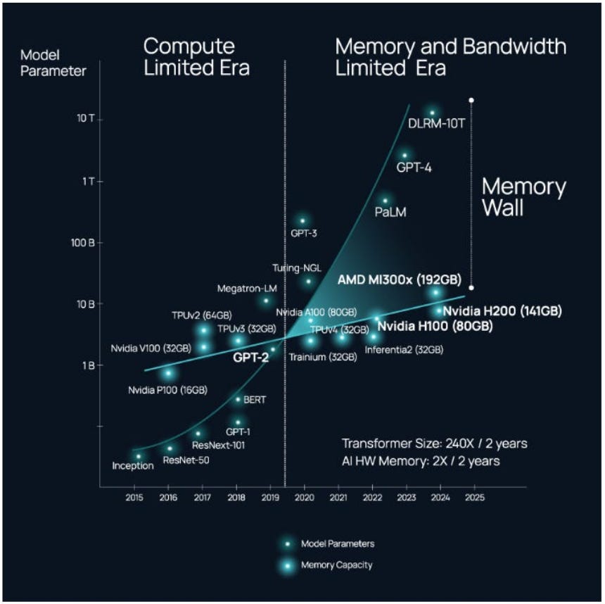
According to Ayar Labs’ glossary, the memory wall arises because processor performance improvements far outpace memory bandwidth growth. Additionally, packaging I/O limitations and signal integrity constraints make memory expansion difficult. While logic transistor density and compute capability have advanced rapidly, DRAM scaling has stagnated. HBM provides higher bandwidth, but it is expensive and limited in supply.

Impact on AI and HPC
AI training and inference demand massive memory bandwidth and capacity. Modern large language models (LLMs) contain tens of billions to trillions of parameters. For example, training GPT-3’s 175 billion parameters in 16-bit precision requires about 3 TB of memory, while trillion-parameter models need around 32 TB.
However, current HBM stacks are limited by chip shoreline I/O and packaging area, which constrain the number of stacks that can be integrated. As model sizes continue to grow, existing architectures struggle to keep up. This creates an urgent need for new memory architectures or higher-density HBM stacking to mitigate the memory wall problem.
Memory Allocation and Expansion under the CXL Architecture
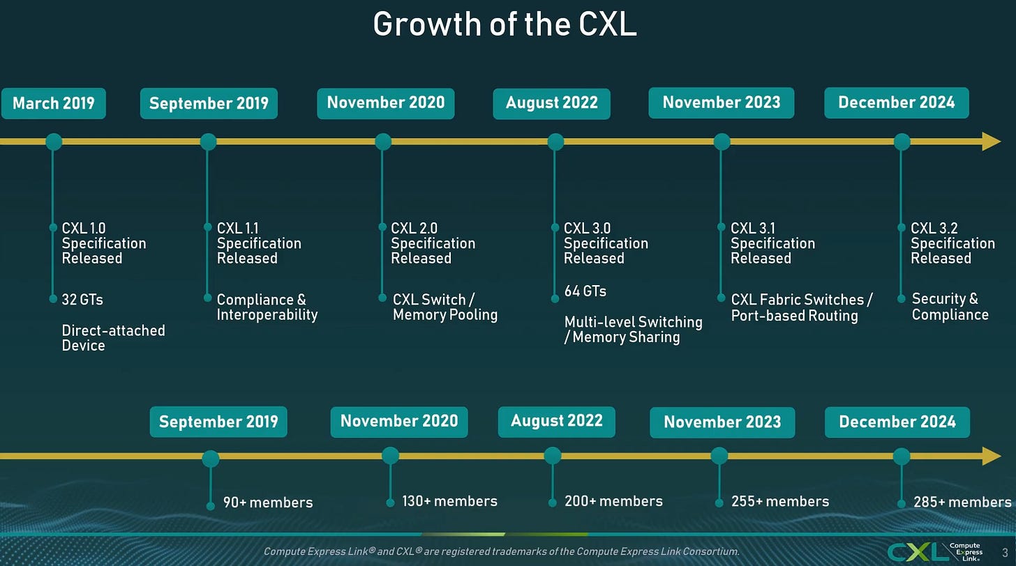
CXL Overview
Compute Express Link (CXL) is an open standard built on the PCIe physical layer that enables high-speed, low-latency, cache-coherent interconnects between processors and devices. CXL consists of three protocols:
CXL.io– Handles basic management and I/O transfers, similar to PCIe.
CXL.cache– Allows external devices to coherently cache host memory.
CXL.mem– Enables the host or device to directly access device memory (e.g., DRAM, Optane, or HBM) using load/store semantics. It supports memory sharing and pooling, allowing dynamic allocation based on workload demands.
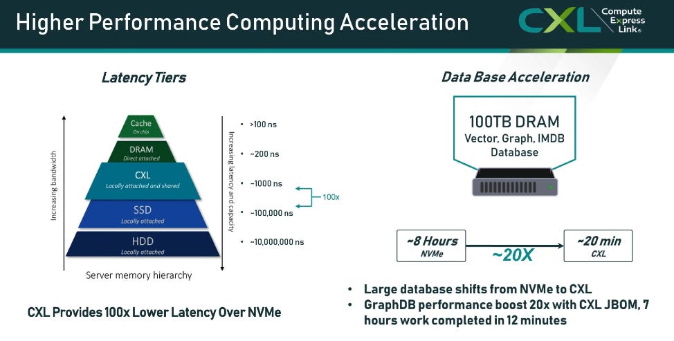
CXL devices are categorized into three types:
Type 1: Accelerators without local memory (e.g., SmartNICs).
Type 2: Accelerators with local memory (e.g., GPUs, FPGAs).
Type 3: Pure memory expansion devices that provide additional memory capacity to the host.
Memory Expansion and Allocation
Starting from version 2.0, the CXL standard supports switching and memory pooling. Memory pooling allows multiple hosts to share a pool of memory devices and allocate memory dynamically as needed. For example, in a data center, a shared CXL memory pool can be created so that different servers can use portions of the pool based on their workloads—without the need to overprovision DRAM for each individual server. This reduces idle memory and lowers costs.
CXL 3.0/3.1 further enhances flexibility by introducing multi-level switching, point-to-point memory access, and support for up to 4,000 nodes in a single fabric, enabling highly scalable and flexible memory sharing.
In practice, CXL memory expansion cards—such as Astera Labs’Leo CXL Smart Memory Controller—connect multiple DDR5 channels to the host through CXL, offering up to 2 TB of capacity and supporting both memory expansion and pooling. This approach can increase memory bandwidth and capacity for AI and database workloads by more than 50%. By enabling dynamic memory allocation, CXL helps eliminate underutilization and overprovisioning, reducing the constraints imposed by the memory wall on overall system performance.
Solutions Combining Optical Chips and Memory
Celestial AI Photonic Fabric
Celestial AI’sPhotonic Fabricuses silicon photonics interfaces to connect compute and memorywithin the package, enabling data transmission at the speed of light. In 2024, the company announced a partnership with hyperscalers to deploy its photonic routing technology, which can deliver data directly to the compute point, supporting the bandwidth demands ofHBM3E and future HBM4.
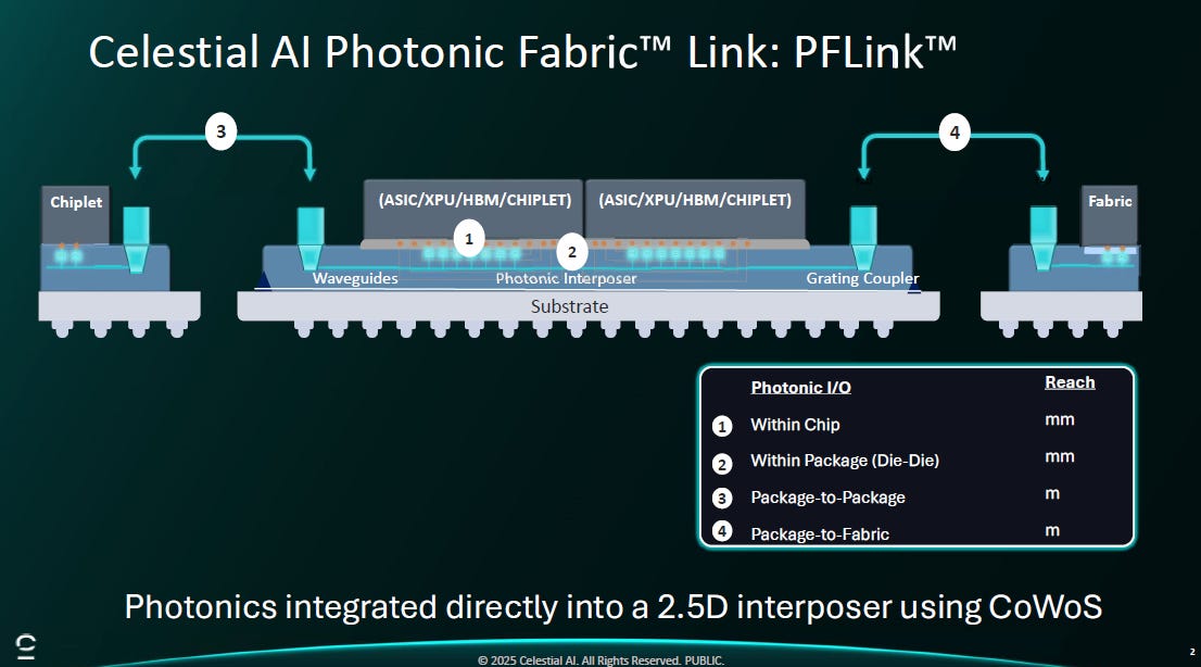
Its memory expansion module integrates72 GB of HBM (two stacks)and four DDR5 DIMMs, expandable to2 TB. The photonic chip provides14.4 Tb/s (1.8 TB/s)endpoint bandwidth with round-trip latency of about120 ns, achieving energy efficiency of6.2 pJ/bit, significantly lower than NVLink and other electrical interconnects.

2025年7月4日
Jim Elliott, VP of Samsung’s Memory Business, noted that this technology can connect large shared memory atHBM speed with nanosecond latency, effectively eliminating the memory wall.
Lightmatter Passage M1000
In 2025,Lightmatterintroduced thePassage M1000, a 3D photonic superchip. The M1000 is amulti-die 3D photonic interposerwith a total area of over4,000 mm², offering114 Tb/sof optical bandwidth. It enables electrical–optical I/O at any point within the package.
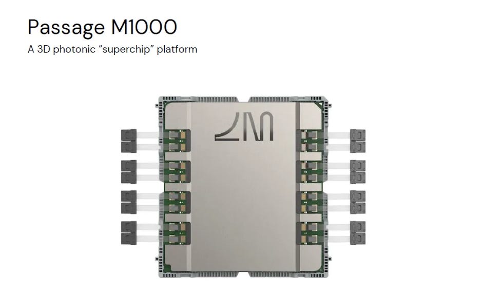
Using areconfigurable waveguide networkand256 optical fibers, it connects thousands of chips into a single domain, overcoming the limitations of chip shoreline I/O. Built on theGF Fotonixplatform, the M1000 features1024 electrical SerDes,56 Gbps NRZ modulation, and8-wavelength WDMtransmission.
This platform allows HBM stacks and compute dies to be integrated into a large composite package, providinghundreds of Tb/sof interconnect bandwidth through optical links — a powerful combination for training large AI models.
2025年8月29日
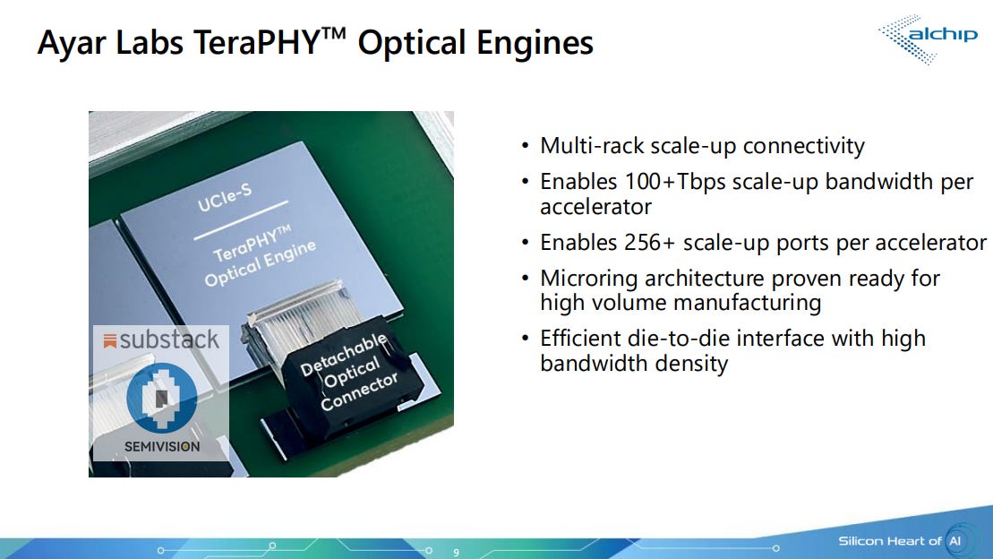
Ayar Labs TeraPHY Optical I/O
Ayar Labs’TeraPHYis a compact, low-power optical I/O chiplet that complies with theUCIe packaging standard. Each chiplet contains8 full-duplex optical ports, with each port consisting of16 WDM transceivers, providing8 Tb/s bidirectional bandwidthand only~10 ns latency.
Compared to traditional copper interconnects, TeraPHY offers5–10× bandwidth,10× lower latency, and4–8× better energy efficiency. When paired with theSuperNova light source, TeraPHY enablesmillimeter-to-kilometer scale connectionsbetween chips and memory, bringing multi-Tb/s interconnect capabilities to AI infrastructure.
Ranovus (Odin) Multi-Wavelength Optical Platform
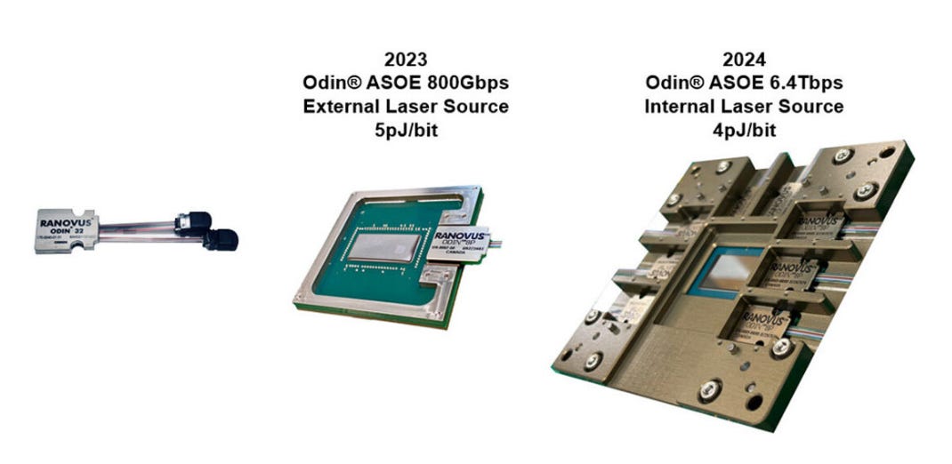
Ranovus’ ODINplatform leverages asingle-chip electronic–photonic integrated circuit (EPIC)that integratesquantum dot multi-wavelength lasersandmicroring resonators, delivering multi-Tb/s optical interconnects.
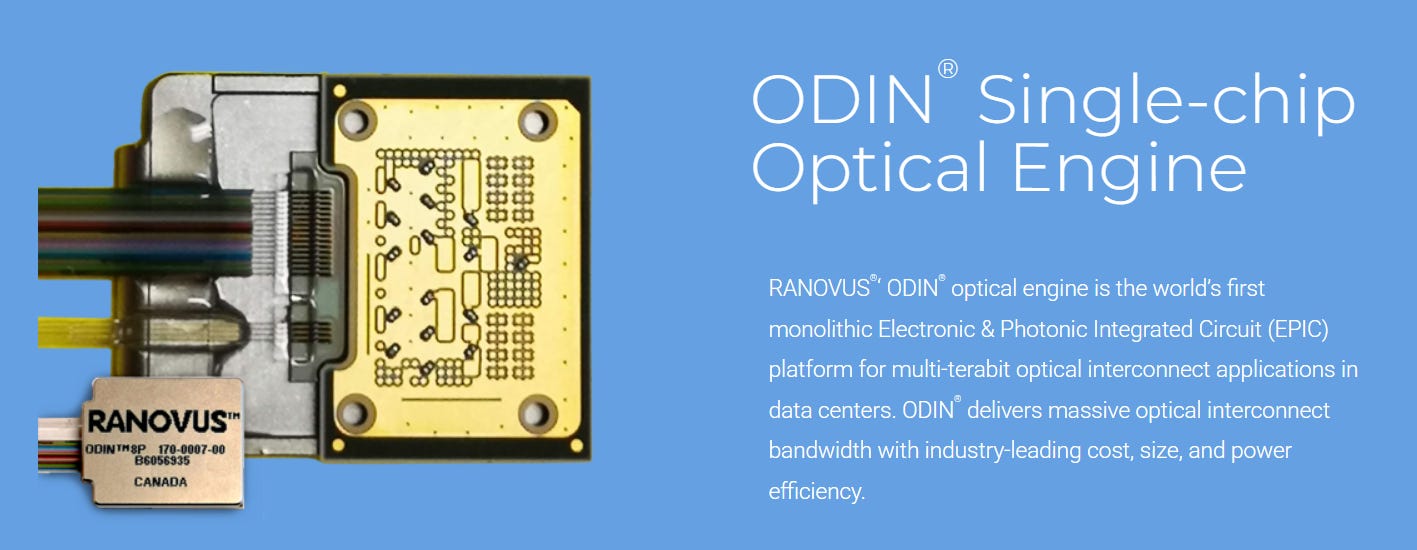
ODIN provideshigh-density, low-power co-packaged opticsfor AI data centers, supporting next-generation packages that combine XPUs and HBM. Through advanced packaging and co-packaged optics, ODIN enableshigh-performance optical links between compute and memory, addressing both thememory wallanddata center power consumptionchallenges.
Academic Research: Optical Multi-Stacked HBM
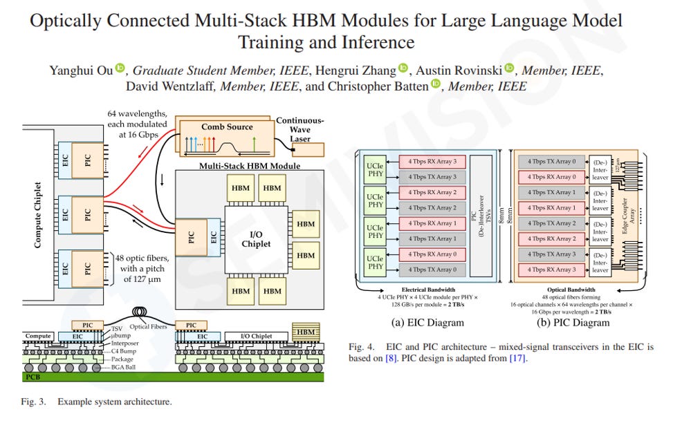
Researchers from Cornell University and other institutions have proposed an optical interconnect architecture for multi-stacked HBM. By co-packaging photonic-electronic interface chips (EIC + PIC) with multiple HBM stacks and connecting them to compute chips via optical fibers, the architecture can scale HBM capacity to 576 GB with 12 TB/s of total bandwidth — all within the existing A100 package footprint.
Simulation results show this approach canimprove training efficiency for trillion-parameter LLMs by 1.4×andboost inference efficiency by 4.2×. This demonstrates thatoptical interconnects can break traditional package area constraints, enabling more HBM stacks beyond the limits set by die perimeters.
Will HBM Be Replaced by Flash? — The Potential of HBF/HFM
While HBM offers extremely high bandwidth, it is limited in capacity and expensive. To address the capacity issue, SanDisk and SK hynix signed an agreement in 2025 to jointly develop theHigh-Bandwidth Flash (HBF)standard. HBF leverages 3D NAND stacking combined with TSV vertical interconnects, enabling parallel access to multiple flash arrays under a logic control layer. Its design goal is to deliver bandwidth comparable to HBM while increasing capacity by 8–16× at a similar cost. SanDisk plans to release samples in the second half of 2026, with the first AI inference devices equipped with HBF expected to appear in 2027.

According to industry information, first-generation HBF stacks can provideup to 4 TB of VRAMon GPUs by parallelizing access across high-capacity 3D NAND arrays to sustain bandwidth. HBF is designed to complement, rather than replace, HBM—targetingAI inference workloadsthat are predominantly read-intensive. However, HBF still faces several challenges:
Higher latency– Flash memory has much higher access latency than DRAM, making HBF unsuitable for training workloads that require nanosecond-level response times.
Limited endurance– NAND flash has write cycle limitations, which may impact workloads with frequent updates.
Protocol differences– Although HBF’s mechanical and electrical interfaces resemble HBM, protocol modifications are still needed, meaning it is not fully compatible.
As a result,HBF/HFM is more likely to serve as a complementary memory layer, providing massive capacity for AI inference or cold data storage, rather than a full replacement for HBM.

SemiVision’s Quick FAQ on HBM & Memory Technologies
Q1: How has HBM evolved across generations, and what are the key features?
A:HBM originated in 2013 with the release of the HBM1 standard by JEDEC. It uses stacked DRAM dies connected through TSVs and a 2.5D silicon interposer, delivering far higher bandwidth than GDDR or DDR. HBM2/2E introduced pseudo-channels and raised speeds to 8 Gb/s per pin. HBM3/3E expanded channels to 16 and supported 64 banks, enabling up to 24 GB per stack. HBM4, launching in 2025, doubles the channel count to 32, with 2,048 I/Os, reduces power by 40%, and adds features like Directed Refresh Management and bus remapping. Future HBM may move toward even taller stacks, higher bandwidth, and hybrid architectures with flash memory.
Q2: What is HBM IP and why is it needed?
A:HBM IP refers to the controller and PHY intellectual property provided by semiconductor IP vendors, allowing SoC designers to integrate HBM interfaces without in-house development. These IP blocks support the latest standards, offering high bandwidth, low latency, and robust data transfer. For example, Synopsys’ HBM4 IP achieves 12 Gb/s per pin and over 3 TB/s total bandwidth. GUC’s HBM4 IP uses proprietary interposer routing and I/O monitoring to ensure signal integrity. With HBM IP, chip designers can rapidly integrate high-bandwidth memory for AI GPUs, datacenter SoCs, and ASICs while reducing development risk and time.
Q3: What is the “Memory Wall” and why does it exist?
A:The Memory Wall refers to the growing gap between processor performance and memory bandwidth. Over the past two decades, GPU compute performance has grown roughly 60,000×, while DRAM bandwidth has only improved by about 100×. As a result, processors spend significant time idle, waiting for data. Causes include stalled DRAM scaling, limited I/O pins, signal integrity degradation, and the high cost of data movement versus computation. HBM alleviates this with high bandwidth, but stacking limits and supply constraints prevent it from fully meeting trillion-parameter AI model demands.
Q4: How does CXL address memory allocation challenges?
A:CXL is a cache-coherent interconnect standard built on PCIe, enabling processors and devices to share memory. CXL.io handles discovery and management, CXL.cache allows devices to cache host memory, and CXL.mem exposes device memory (e.g., DDR5 or HBM) directly to the host. Starting with CXL 2.0, memory pooling and switching are supported—multiple CXL memory devices can form a shared pool for dynamic allocation across servers. For example, Astera Labs’ Leo CXL controller aggregates multiple DDR5 channels into a single card with up to 2 TB capacity, supporting both expansion and pooling. This enables datacenters to scale memory on demand, reduce stranded resources, and ease memory wall constraints.
Q5: How can optical chiplets and photonics help overcome the Memory Wall?
A:Optical chiplets or photonic interposers use silicon photonics waveguides to link compute and memory modules, offering tens of times more bandwidth than electrical wires with lower latency. Celestial AI’s Photonic Fabric treats HBM as a high-speed cache while connecting large DDR5 memory banks optically to compute dies—providing 1.8 TB/s bandwidth, 120 ns round-trip latency, and 6.2 pJ/bit energy. Lightmatter’s Passage M1000 uses a 3D photonic interposer with 114 Tb/s bandwidth and 256 fibers, breaking the chip perimeter bottleneck. Ayar Labs’ TeraPHY optical I/O chiplet provides 8 Tb/s per chip at ~10 ns latency, while Ranovus’ ODIN platform uses quantum-dot lasers and microring resonators for multi-wavelength interconnect. These solutions extend HBM beyond the package or connect multiple memory modules, boosting bandwidth while lowering power and latency—effectively breaking the Memory Wall.
Q6: Will Flash replace HBM in the future?
A:To address HBM’s limited capacity and high cost, SanDisk and SK hynix proposed theHigh-Bandwidth Flash (HBF)concept. HBF stacks multiple 3D NAND dies with TSVs, offering HBM-like bandwidth but 8–16× the capacity. First-generation products are expected to enable up to 4 TB of GPU VRAM. However, flash has higher latency and lower endurance, so HBF targets read-intensive AI inference workloads rather than replacing DRAM-based HBM entirely. Long-term roadmaps (e.g., HBM8) envision hybridHBM + HBF/HFMarchitectures, where HBM acts as a low-latency cache and HBF provides large, cost-efficient capacity for cold data or inference.
Through3D stacking and silicon interposers, HBM has revolutionized memory bandwidth but remains limited by stack height and supply constraints. As AI models grow explosively, the Memory Wall has become a core system bottleneck.CXLtackles this at the system level with pooling and coherency, whilephotonicsaddresses it at the package level with massive bandwidth and low latency. The future likely lies in amulti-tier memory hierarchycombining HBM, high-bandwidth flash, and optical interconnects—enabling AI systems to finally break through the Memory Wall.
Technology Advancement for Performance Boost in TSMC’s viewpoints

The surging demand for AI chips is driving the entire semiconductor supply chain towardlarger areas, higher bandwidth, and greater power density. For example, the die size of individual GPUs and AI ASICs is now approaching800 mm², with final package modules often exceeding100 × 100 mm. This places unprecedented design pressure on bothinterposersandABF substrates.
These high-power AI chips must simultaneously achievehigh-speed signal transmission,low-latency power delivery, andefficient thermal managementwithin the packaging stack.
Signal integrity:To support hundreds of GB/s of chip-to-chip communication (e.g., GPU-to-HBM or GPU-to-GPU), the interposer requires ultra-dense RDL routing and stable electrical characteristics. TSMC’sCoWoS-LandCoWoS-Rhave emerged as key solutions.
For example, to meet224 Gb/s+ SerDes interfacesand4–8 TB/s HBM bandwidthdemands, CCL materials must simultaneously deliverlow Dk/Df,low surface roughness,high thermal stability, and optimizedZ-axis expansionto minimize loss and latency at high frequencies. However, these electrical enhancements also intensifythermal pressure— with AI chips now routinely exceeding500–1000 W/cm² heat flux, traditional TIM and air-cooling modules are no longer sufficient. The industry is rapidly shifting towardliquid cooling,micro-channel cold plates (MCLP),SiC thermal substrates, anddiamond thin-film heat spreaders.
2025年10月5日

2025年9月21日
Aspackaging and thermal modules reach physical limits,memory placement and allocation (HBM Allocation)has become the new bottleneck. Modern AI GPU modules typically integrate6–8 HBM stacks, but within the limited interposer area, simultaneously achieving optimalsignal path length,power distribution uniformity, andthermal balanceis increasingly difficult. SemiVision’s earlier analysis shows that HBM performance bottlenecks often stem not from the DRAM itself, but fromRDL routing congestionandpower noise distribution.

To address this, TSMC and major GPU vendors are adoptingasymmetric HBM placement,localized power delivery networks (PDN), andmulti-layer RDL stack-up optimizationsto maximize bandwidthwithout increasing interposer size.
NVIDIAuses asplit interposerarchitecture in CoWoS-L packaging to keep HBM signal paths localized, reducing insertion loss from long traces.
AMDandBroadcomare experimenting with integratingPower Redistribution Networks (PRN)into the substrate layer to further reduce high-frequency noise and IR drop.
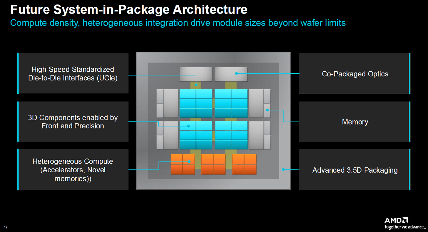
These design trends all point toward a critical shift:AI chip performance gains no longer depend solely on logic scaling, but increasingly on theco-optimization of packaging, substrate, memory, and power delivery.
In short, asinterposer area is constrained by reticle size and cost, the key challenge for next-generation AI chip architecture is how tomaximize HBM bandwidth utilization and dataflow efficiency within a fixed package footprint. This will not only determine the performance of individual GPUs but will also directly impact theperformance-per-wattandcost structureof entire AI systems.
HBM Allocation and Packaging Space Optimization Strategies
Asinterposer areaandABF substratedesigns approach their physical and cost limits, the ability tomaximize HBM bandwidth and power delivery efficiency within limited spacehas become the next key battleground for advanced AI packaging.

In today’s high-end GPUs, the logic die already occupies the majority of the interposer area. As a result, theplacement of HBM stacks (allocation)must be precisely engineered to avoid routing congestion, increased latency, and reduced power efficiency.
- Asymmetric HBM Placement
Traditionally, GPU modules adoptsymmetric HBM configurations(e.g., 4+4 or 6+6 around the logic die) to enable uniform signal routing. However, as interposer area becomes constrained andRDL routing pressureincreases, the industry is moving towardasymmetric layouts.
In these designs,high-bandwidth and latency-sensitive HBM stacksare placed closer to critical I/O hotspots (such as chiplet-to-chiplet SerDes regions), while less critical memory modules are allocated to secondary zones. This shortens critical signal paths and reduces insertion loss.
The main challenge lies in maintaininguniform PDN (Power Delivery Network)andSI/PI (Signal/Power Integrity). TSMC has addressed this on its CoWoS-R/L platforms by introducingsegmented PDN architectures, allowing each HBM region to have relatively independent power and decoupling networks. This minimizes local IR drop or power noise from impacting global performance.
- Multi-layer RDL Stack-up and Routing Zoning
With HBM speeds reaching9.2–12.8 Gbps per pin(and potentially exceeding 16 Gbps/pin with HBM4),single-layer RDLcan no longer accommodate the thousands of high-speed signal traces required.
TSMC has adoptedmulti-layer RDL stack-upsthat:
Placehigh-speed differential pairsin the inner layers.
Use outer layers for power distribution and low-speed control signals.
This structure helps to:
Reduce coupling and crosstalk for high-speed signals.
Stabilize impedance and routing uniformity.
Precisely control delay and jitter.
Increase routing density without expanding interposer size.
Additionally, TSMC has introducedRouting Zoningin CoWoS-R, partitioning RDL layers into functional zones (HBM zone, SerDes zone, Clock/Power zone). This reduces trace length and crosstalk while enabling localized optimization.
- SI / PI Simulation and Verification Flow
Such dense designs demand rigorouselectrical simulation and validationfrom the early design stage, using full-wave 3D simulation tools (e.g., Ansys SIwave, HFSS, Cadence Sigrity) to analyze:
HBM–SoCS-parameters(reflection/insertion loss).
PDN noise suppression with decoupling capacitor configurations.
Routing length impact onlatency and jitter.
Effectiveness of cross-layer grounding for EMI/crosstalk mitigation.
Following simulation, TSMC and customers useCoWoS-R as the physical validation platform, performingeye diagram measurements,BER testing, andpower noise spectral analysisto ensure the design can sustainhigh yield and reliabilityin volume production.
- System Technology Co-Optimization (STCO)
Ultimately, this is no longer the sole responsibility of packaging teams. It has evolved intoSTCO (System Technology Co-Optimization), whereHBM placement,RDL routing,PDN distribution, andthermal structuresmust beco-optimized with the logic I/O architecture, bandwidth demands, and system-level cooling.
This is why companies such asTSMC, NVIDIA, and AMDhave established dedicatedPackage Architecture Teamsto bridge front-end design, packaging, and system validation.
In the AI-driven era ofhigh-speed packaging,HBM allocationhas evolved from a simple stacking decision into amulti-dimensional design challengeinvolving electrical integrity, routing architecture, and system thermal management.
This will be a decisive front in the competition amongCPO/OIO, high-speed interconnect, and advanced packaging platforms.
Notably, atHot Chips 2025, Marvell VP of TechnologyMark Kuemerlepresented“A Revolution in Memory Architecture for the Data Center”, highlighting the company’s innovations inSRAM and HBM architectures. Marvell’s technical blogs further detailed theircustom HBMandCXLstrategies. Below is a summary comparing their perspectives on future memory architectures.
Marvell :SRAM — Boosting Bandwidth and Efficiency in AI/XPU Devices
2 nm High-Density SRAM
Marvell’s key SRAM IP is among the first to tape out at every major process node, providing developers with early hardware validation platforms. The company’s high-density SRAM is manufactured on its 2 nm platform and deployed in XPUs, network switches, and NICs for data center applications.

Lowering Vmin and Enhancing Reliability
To reduce power consumption, Marvell optimized Vmin (minimum operating voltage) on its N2P hardware, achieving the lowest Vmin ever recorded for ultra-dense bitcell memory. This was accomplished through a combination of circuit design techniques including write-assist, stability-assist, high-sigma modeling, and row/column redundancy. These innovations not only reduce power but also improve manufacturing yield.
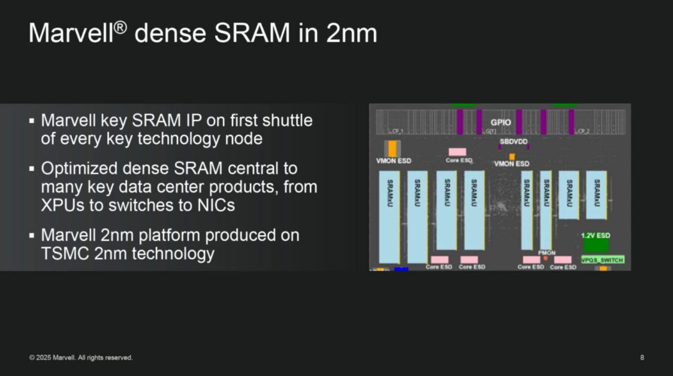
Benefits of Custom SRAM
Marvell compared its in-house 1 Mb high-density SRAM to third-party memory and found that, at equivalent bandwidth, its solution achieves50% smaller area,66% lower standby power, and17× higher bandwidth per unit area. These advantages make SRAM an ideal embedded memory for AI accelerators and network switches.
To deliver such high bandwidth, Marvell uses three strategies:increasing operating frequency,widening data access width, andadding more ports. Experimental results show that, using the same memory array and bitcell, Marvell’s SRAM achieves a significantly higher bandwidth-per-area ratio than industry standards across different capacities.
Silicon validation demonstrates that Marvell’s custom N3P high-density SRAM maintains strong PVT (process, voltage, temperature) margins, proving its manufacturability.
Marvell views high-density SRAM as afoundational building blockfor AI accelerators. By leveraging advanced 2 nm processes, low-Vmin circuit techniques, and superior bandwidth-to-area efficiency, Marvell’s embedded SRAM can complement external memory like HBM, playing a critical role in high-performance computing architectures.
Marvell:Custom HBM — Tailoring Memory to Match XPU Requirements
Limitations of Standard HBM
Traditional High-Bandwidth Memory (HBM) consists of stacked DRAM dies and a base die that houses the I/O interface and memory controller. Standard HBM4 designs feature 32 × 64-bit channels, resulting in a large I/O footprint and high power consumption.
In XPU designs, HBM can consume up to25% of die areaand account for40% of total cost. As memory capacity scales from80 GB to 288 GB and beyond, the power and area overhead of standard HBM becomes a major constraint.
Marvell’s Custom HBM Architecture

Concept: Marvell proposes a“Custom HBM”architecture that redistributes traditional HBM functionality:
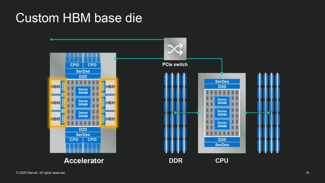
Replaces the standard HBM PHY with adie-to-die (D2D) PHY, moving the HBM memory controller onto thelogic base die.
AddsAI-specific D2D channels, RAS/telemetry monitoring, and Quality-of-Service (QoS) modules on the logic base.
This allows memory interfaces to be tailored to the XPU’s specific compute characteristics, placing critical logic and transport closer to where it’s most effective.
Benefits:
More usable compute area:Standard HBM XPUs allocate a large portion of silicon to I/O. With Custom HBM, Marvell reports a1.7× increase in usable compute area, with the option to place compute chiplets directly on the HBM base for higher compute density.
Reduced I/O power:By shifting interfaces to D2D links, I/O power between HBM and the main die can be cut by~75%.
Scalable memory–compute integration:Mapping standard HBM channels to D2D links allows future expansion with additional memory, logic, or accelerator chiplets.
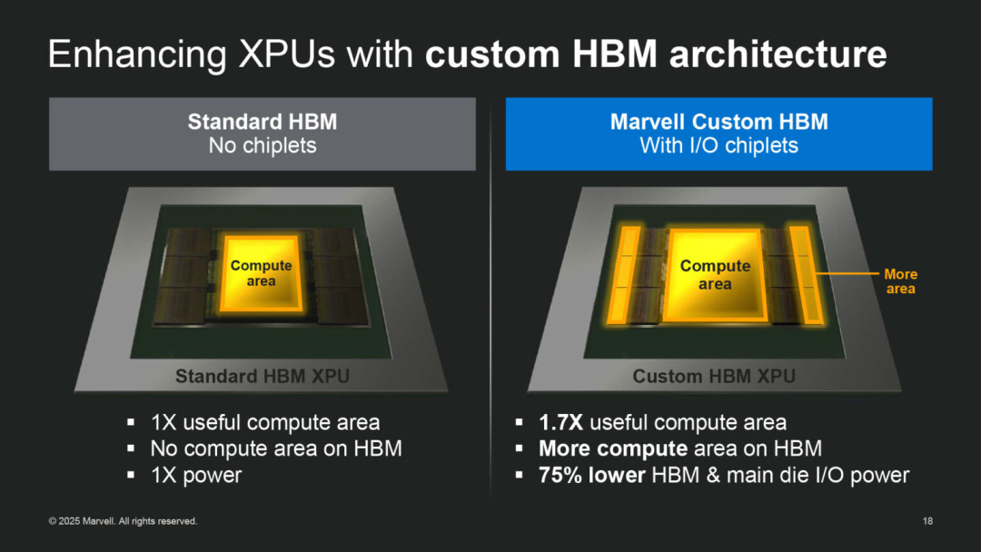
Example:Marvell notes in its blog that Custom HBM canincrease on-package memory by 33%,cut interface power by 70%, andfree up 25% of chip areafor compute logic. Depending on the use case (e.g., edge inference vs. large-scale training), designers can adjust HBM controller and PHY sizing to reduce I/O footprint or boost channel count.
D2D Technology Support

Marvell emphasizes its D2D interface IP as the enabler of Custom HBM.
In Q2 2023, Marvell demonstrated32 GbpsD2D transfer speeds—well ahead of industry standards scheduled for volume production in 2025.
In August 2025, Marvell announced theindustry’s first 64 Gbps/pin bidirectional D2D interface IP, offering>3× the bandwidth densityof UCIe, with intelligent power management to reduce power spikes under burst traffic.
These D2D advances underpin Custom HBM, enabling higher bandwidth within a smaller I/O footprint while lowering error rates and power consumption.
Comparison with Standard HBM
Marvell compared standard HBM with Custom HBM in its December 2024 blog, highlighting dramatic reductions ininterface areaandpower, along with fewerµ-bumpsand power/ground bumps required.
Thecore enableris the high-speed D2D interface and the ability tocustomize the memory controllerto fit specific XPU requirements. Marvell predicts that by2028, around25% of accelerated compute chipswill adopt custom architectures, includingCustom HBM,custom XPUs, andCXL controllers.
Marvell : CXL — Expanding and Sharing Memory Through Compute Express Link
CXL Overview and Principles
Marvell notes in its blog that since the invention of magnetic memory in the 1950s and DRAM in the 1970s, there have been few major breakthroughs in the memory field.CXL (Compute Express Link)represents the next major leap.
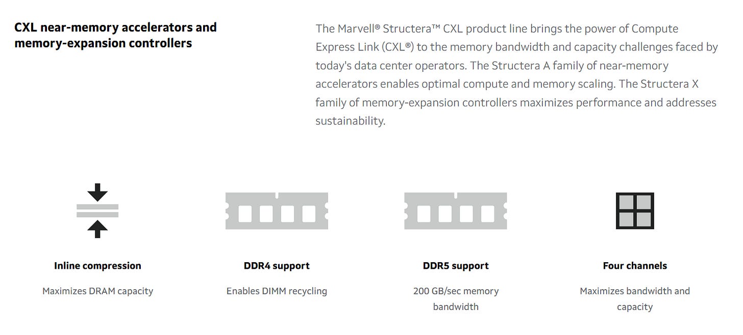
Marvell: CXL Near-Memory Compute and Expansion
CXL devices use the existing PCIe physical interface to open aparallel channel to the processor’s memory bus, providing additional lanes and higher data throughput to relieve the burden on the congested memory fabric.
Structera A: Near-Memory Accelerator
Near-memory accelerator (Structera A)— Marvell’s Structera A is a new type of CXL near-memory accelerator that integrates16 Arm Neoverse V2 cores, delivering200 GB/s of memory bandwidththroughfour DDR5-6400 channels, each supporting two DIMMs.
Benefits:
Plugging one Structera A into an x86 server increasescore count by 25%(from 64 to 80), boostsbandwidth by 50%(400 Gbps → 600 Gbps), and expandsmemory capacity from 2 TB to 6 TB, with only a100 Wpower increase.
Energy per GB/s of transfer drops by17%.
Installing two accelerators increases core count by50%, doubles bandwidth, and boosts capacitysixfold.
Rack-level scaling:
Installing40 Structera A units per rackcan add3,840 processing coresand24 Tbps of memory bandwidthto existing servers —without expanding the data center footprint, thereby reducing infrastructure and cooling costs.
Structera X: Memory Expansion and DDR4 Reuse
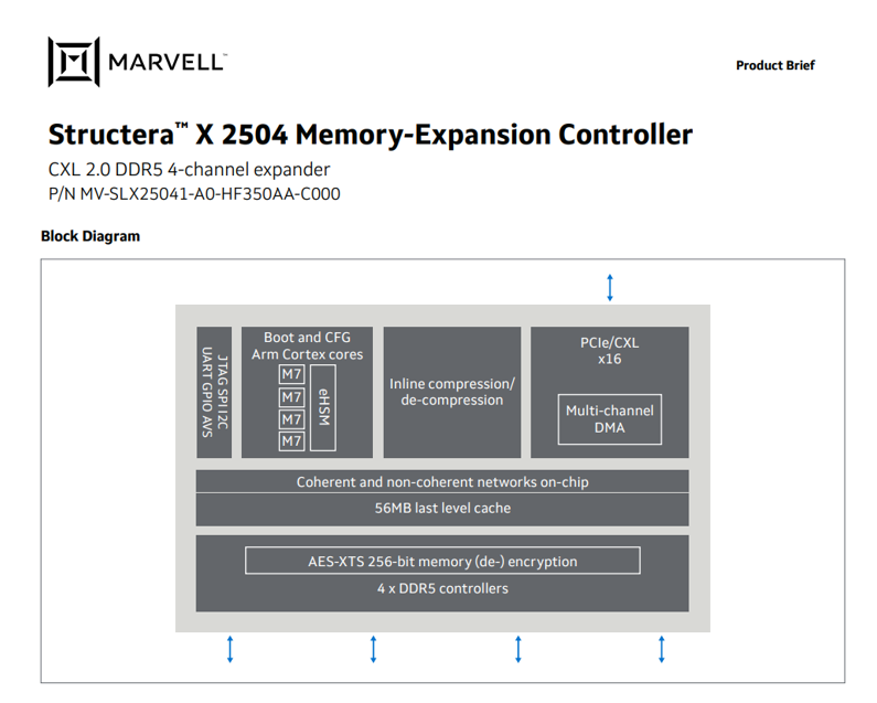
Memory Expansion Controller (Structera X)— CXL enables servers to attach external memory expansion devices. Structera X supportsDDR5 or DDR4, with up to200 GB/s bandwidth. The DDR5 version supportsup to 3 DIMMs per channel, for over6 TB capacity; the DDR4 version supports3 DIMMs/channel, enabling up to4 TB capacity.
DDR4 reuse example:
Next-generation servers may only support DDR5, but there remains a large pool ofdecommissioned DDR4 DIMMs. Structera X can connect12 DDR4 DIMMsthrough CXL, offering6 TB capacity, orup to 12 TBwith LZ4 compression. This reduces costs, extends the life of existing memory, and cuts electronic waste.
Five Key Impacts of CXL

Accelerating DLRM and Inference Workloads
CXL alleviates memory bandwidth bottlenecks. Structera A provides extra cores and high bandwidth near memory, improving the efficiency ofDeep Learning Recommendation Models (DLRM)and other inference tasks.
Reducing Data Center Footprint and Infrastructure Costs
By expanding compute and memory through CXL,one rackcan achieve the capacity of many servers, cutting space and cooling demands.
Reusing Idle Memory
CXL enables the reuse of DDR4 memory through Structera X, allowing 12 DIMMs to be configured per server. Compression further boosts capacity, reducing the need for expensive DDR5 procurement.
Improving Asset Utilization via Memory Pooling
CXL allowstwo processors to share a single Structera X memory expansion, forming amemory pool. Microsoft estimates~25% of server memory sits idlebecause it is tied to a single CPU; CXL pooling cansave 5–9 TWhof data center power annually by reducing this stranded capacity.
Telemetry-Driven Operations
Future CXL devices will include telemetry to monitor memory pools and distributed systems, improvingresource allocationandpredictive maintenance.
Marvell’s Perspective
Marvell seesCXL as a key technologyto overcome both memory bandwidth and capacity bottlenecks.
Structera Aoffers near-memory compute and bandwidth for AI inference workloads.
Structera Xprovides flexible memory expansion, supporting DDR5 while enabling cost-effective DDR4 reuse.
CXL’smemory pooling and telemetry capabilitiesreduce idle resources and improve sustainability.
Together, these features enablemore scalable, efficient, and flexible AI infrastructure, marking a major architectural shift in data center memory systems.
Integrated Perspective: Marvell’s Memory Strategy
From Marvell’s presentations and blog posts, the company’smemory architecture strategycan be summarized into the following key pillars:
- Optimizing Every Tier of the Memory Hierarchy
On-chip:
Marvell leverages2 nm high-density SRAMcombined with advanced circuit techniques to lower power and area while delivering ultra-high bandwidth. These SRAM blocks act ascaches or scratchpads for XPUs, improving core utilization and efficiency.
Stacked-chip level:
Marvell proposesCustom HBM, which re-architects the HBM base die and I/O interface and pairs it with Marvell’s proprietarydie-to-die (D2D)technology. This approach frees up compute area, reduces power consumption, and supports future HBM standards, enablingmore flexible and application-tailored AI accelerators.
System level:
ThroughCXL, Marvell enablesnear-memory acceleration and memory expansion, using itsStructera A/Xproducts to support various workloads such as inference, training, and databases. At the same time,memory pooling and flexible resource allocationare achieved across servers.
- Lowering Total Cost of Ownership (TCO)
By reducingSRAM Vmin, cuttingI/O power in custom HBM, and enablingmemory reuse through CXL, Marvell significantly reduces overall power consumption, contributing to lowerdata center TCO.
CXL expandscore counts and memory capacitywithout requiring new physical infrastructure. Reusing DDR4 DIMMs through Structera X further saves onprocurement and disposal costs.
- Customization and Modularity
Marvell anticipates a future withgreater customization across XPUs, HBM, CXL controllers, and NICs. Custom HBM is part of this trend, allowing chip designs to befine-tuned to specific application needs.
- Memory-Centric Data Center Evolution
Marvell’s combination ofhigh-density SRAM,custom HBM, andCXL architecturesoutlines amemory-first roadmapfor data center evolution:
frombitcell innovations at the silicon level,
tointerface customization in stacked memory,
tocross-server memory sharing at the system level.
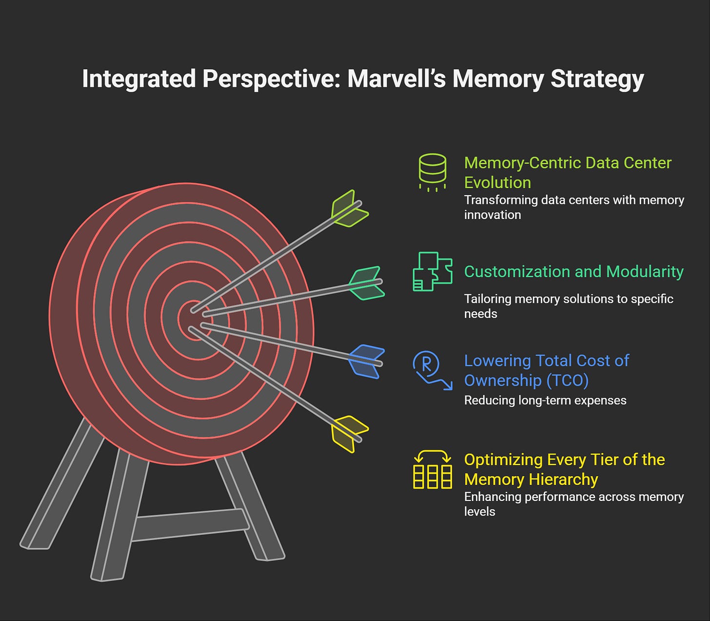
Marvell’s message is clear:“Memory is the only thing that matters.”
This comprehensive optimization strategy not only addresses AI accelerators’ demand forhigh-bandwidth, low-power memory, but also reduces data center energy use and cost, underscoring thecentral role of memory architecture innovationin the future of computing infrastructure.

2025年7月9日
We observe thatBroadcom,Marvell Technology, and multiple AI chip suppliers are actively helping majorcloud service providers (CSPs)adopt and integrateadvanced packaging technologies. This effort has evolved far beyond traditional packaging manufacturing—it is now transforming intofull system-level platform collaboration.

2025年6月4日
These semiconductor vendors are not only supporting customers inchiplet integrationat the packaging level, but are alsoco-developing customized memory subsystems, such ascustom HBM base dies,custom SRAM, andhigh-speed cache architectures. These tailored designs optimizepower consumption, bandwidth, and latency, aligning precisely with thediverse architectural requirementsof different cloud computing platforms.

More strategically,Broadcom and Marvell have incorporated Optical I/O technologiesinto theirAdvanced Package Platform roadmaps, enablinghigher-bandwidth and lower-latencydata transmission betweenAI chips, memory, switches, and accelerators. This marks a fundamental shift: advanced packaging is no longer just a physical integration vehicle for a single chip—it is becoming theinterconnect backbone of high-performance computing systems, directly determining theperformance and energy efficiencyof AI data centers.
Overall, thisjoint development model of “customized memory + packaging + optical interconnect”signals that the industry is rapidly moving fromsingle-chip competitiontowardplatform-level strategic integration. It also reflects thedeepening partnerships between CSPs and the semiconductor supply chain, which will shape the next generation of AI infrastructure.
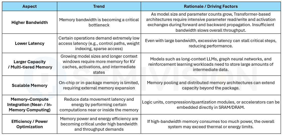
In addition, some studies have specifically addressed thebandwidth bottlenecks of CXL-based memory in LLM inference, proposing aCXL-NDP (Near-Data Processing)architecture. This approach performs operations such ascompression, quantization, and bit-plane layout processingdirectly inside the CXL memory module, thereby improving the utilization of “effective bandwidth.”
Experiments showed that this method canincrease throughput by 43%andextend context length by 87%. This clearly reflects that future AI memory requirements will not only depend onraw bandwidth and capacity, but also onintelligent processing at the memory-module levelto enhance efficiency.
In summary:Future AI chips will demand memory systems that combineultra-high bandwidth,ultra-low latency,large capacity,scalability, andin-memory intelligence.

Amid the rise of generative AI, the choice of compute architecture is undergoing a profound transformation.
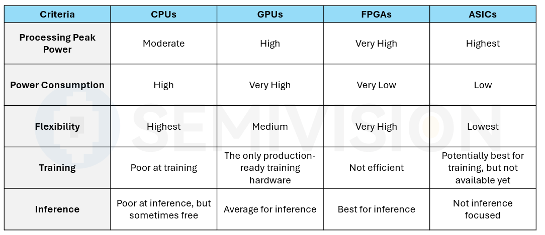
Traditionally,CPUshave handled general-purpose control and logic processing, making them suitable for multitasking and unstructured workloads.GPUs, originally designed for graphics rendering, excel at parallel computing. With the advent of the CUDA platform and the popularization of deep learning, GPUs have become thede facto core for AI training.FPGAsoffer reconfigurable logic flexibility and can be reprogrammed after manufacturing, but they come with higher development complexity and cost.
ASICs (Application-Specific Integrated Circuits)represent a different direction—sacrificing flexibility for extreme efficiency. ASICs are designed for specific algorithms and applications, implementing only the necessary circuitry to achieve their functions. As a result, they offer significant advantages inpower consumption and cost.
As AI models grow larger andinference power consumption and latency become bottlenecks, more companies are turning to ASIC architectures to achievehigher energy efficiency and predictable deployment costs. The GPU-dominated compute revolution is gradually evolving into a“GPU + ASIC coexistence” era.
Advantages and Limitations of ASICs in AI Inference
AI workloads can be broadly divided intotrainingandinferencephases.
Trainingemphasizes flexibility and generality. GPUs dominate this phase because they support a wide range of deep learning frameworks and dynamic model development.
Inference, in contrast, involves fixed model architectures, and the main challenge is toachieve higher throughput with lower power and cost—precisely where ASICs excel.
The greatest strength of ASICs isefficiency. Because their architecture is tailored to specific algorithms or models, ASICs caneliminate unnecessary general-purpose modules, shorten data paths, and minimize power usage. Once mass production begins, theirunit cost can be lower than GPUs or FPGAs. Moreover, ASICs’ tightly controlled and closed circuitry gives themadvantages in hardware security and operational stability.
However, ASICs also havenotable drawbacks.
Theirdevelopment cost is extremely high—including design, EDA licensing, IP procurement, and tape-out—often reaching tens or even hundreds of millions of NT dollars.
They lack flexibility; if the underlying AI model changes, the ASIC may not support new algorithms.
Therapid iteration cycle of AImeans ASIC development timelines can lag behind market needs, requiring careful evaluation ofapplication lifetime and return on investmentbefore committing.
As a result, ASICs arenot intended to replace GPUs, but tocomplement themby providing optimized solutions forspecific, stable, and large-scale applications. For workloads such asrecommendation systems, speech recognition, or large language model inference clusters, ASICs can deliver significant benefits.
Comparison and Complementarity of Compute Architectures
As compute architectures evolve, acomplementary landscapehas emerged amongGPUs,ASICs, andnext-generation high-bandwidth accelerators(such as LPUs or specialized memory-processing chips).
GPUsremain the dominant platform due to theirflexibility and general-purpose programmability, making them well-suited for a wide range of deep learning frameworks and precision modes.
ASICs, on the other hand, excel inlow-precision inference,power-constrained edge deployments, orlarge-scale rollouts, offering superior energy efficiency in these targeted use cases.
Modern GPU systems are also rapidly advancing. For example,NVIDIA’s NVLink technologyprovides up to1.8 TB/s of chip-to-chip interconnect bandwidth, dramatically reducing communication latency in multi-GPU systems. This keeps GPUs at the forefront for large-scale training and distributed inference workloads.
In practice, many companies are adopting a“GPU for training, ASIC for inference”dual-track strategy, balancing flexibility and efficiency. Thishybrid deployment modelis increasingly becoming the mainstream approach for bothcloud and edge AI.

Why are major tech giants investing in custom ASICs?
As thecost structure of AIshifts, major cloud and device companies—includingGoogle, Amazon, Meta, Tesla, Alibaba, and Huawei—are all developing their own ASIC chips. This is driven not only by technical optimization but also bycost control and strategic business considerations.

The traditional chip supply chain involveshigh licensing, manufacturing, and marketing costs. When AI deployments scale tohundreds of thousands of GPUs, even minor efficiency gains can translate into massive operational savings.
Google’s TPU,Amazon’s Inferentia,Tesla’s Dojo,Alibaba’s Hanguang, andHuawei’s Ascendchips are all designed for specific AI workloads, reducing power consumption and data movement latency while improving performance-per-watt.
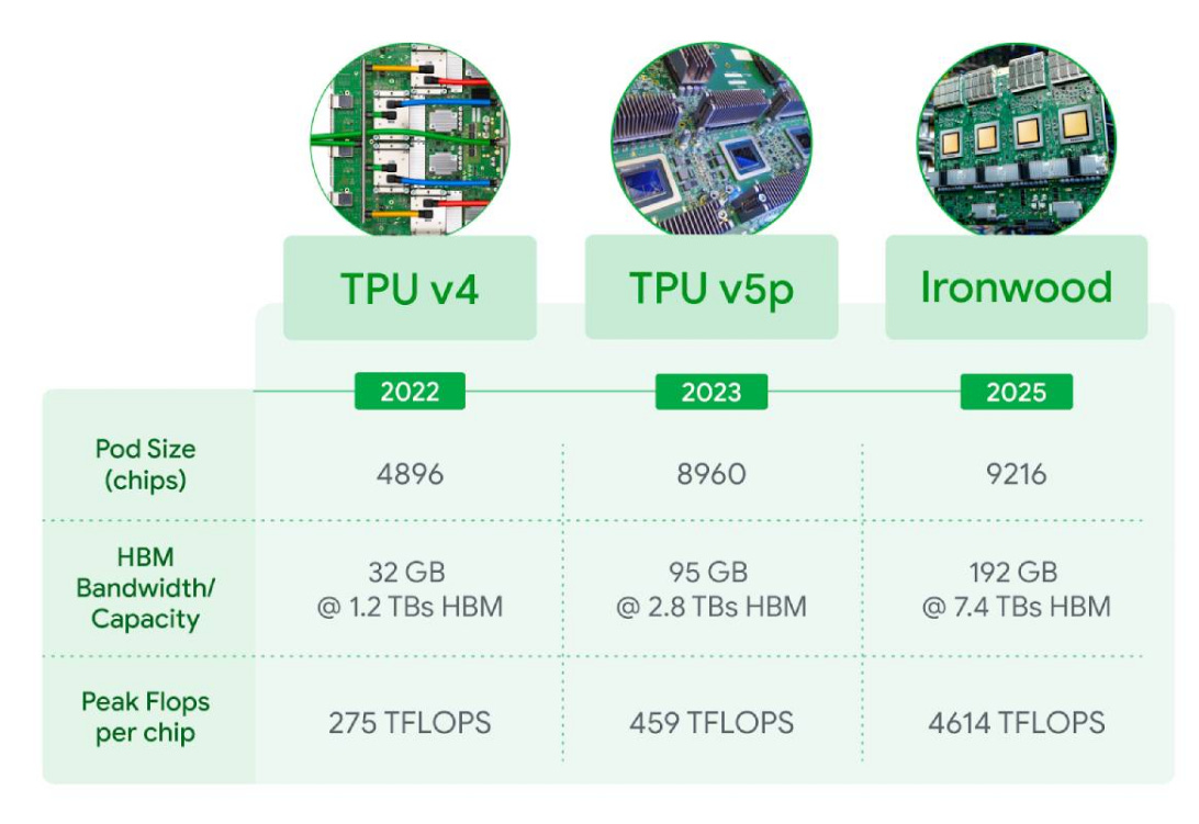

Furthermore,inference is increasingly becoming the primary source of AI revenue. Industry data shows thatinference-related revenue now accounts for over 40% of NVIDIA’s data center revenue. This gives companies a strong incentive todevelop in-house ASICs, reducing long-term dependency on GPUs and mitigating supply chain and cost risks.
Taiwan and China’s Deployment in the AI ASIC Sector
Key Players in the Asian Supply Chain.
In Taiwan,Alchiphas built a strong position in the high-performance ASIC segment through its expertise in custom AI SoCs, 3DIC, andhybrid bondingdesign flows.GUC (Global Unichip)leverages its close partnership with TSMC to gain a competitive edge in advanced-node SoC integration, becoming a key partner for global chip design and manufacturing.

Broadcom, with its strength in networking and interface IP, has solidified its leadership in AI data center interconnect chips.Marvellfocuses on high-bandwidth, low-latency ASIC products by combining HBM andco-packaged optics (CPO)in its designs.
On the China side, companies such asAlibaba,Cambricon, andHuaweicontinue to invest in in-house AI chip development, gradually expanding their reach into inference and edge applications.

These developments indicate that competition in AI ASICs has transcended individual companies — it is now a contest ofentire supply chain integration and process ecosystems.
ASIC WAR : The Race Toward Specialization and Systemization
The rise of ASICs signals that AI computing has entered an era of specialization and system-level optimization. The competition is no longer just about transistor density or process nodes — it’s about who can achieve system-level optimization across memory bandwidth, interconnect efficiency, and packaging integration.
GPUs will continue to dominate the general training market, but ASICs will play a critical complementary role in large-scale inference and specialized workloads. Future AI infrastructure is likely to be aheterogeneous ecosystemcomprising GPUs, ASICs, optical interconnect modules, andCXL-based memory architectures.
For chip design companies, entering the ASIC domain requires not only co-design capabilities between circuits and algorithms, but also the ability to navigate challenges acrosspackaging, process technologies, EDA, IP, and interconnect protocols. Only companies withsystem thinkingcan stand out in this next-generation compute race.
The Impact of the AI Chip Era on Memory and HBM
Architectural Differentiation of AI Chips: The Prelude to the Memory–Compute Bottleneck
CPU, GPU, FPGA, and ASIC Architectural Roles
CPUs and GPUs are mostly based on thevon Neumann architecture, where computation and memory share a single bus for data transfer. This provides high generality but relatively low efficiency.
FPGAs and ASICs, on the other hand, typically adoptHarvard architectures or custom designs, bringing compute units closer to memory to optimize power consumption and performance for specific tasks.
GPUs leverage massive parallel processing units combined withHBM memoryand high-bandwidth interconnects such asNVLinkto deliver exceptional training performance. NVLink 5.0 provides up to1.8 TB/s per card, while PCIe 5.0 ×16 is limited to about128 GB/s.
ASICs are optimized for specific workloads (e.g., matrix multiplication) through dedicated hardware pipelines. They deliverhigher energy efficiency and lower latencythan GPUs, with lower power and cost — but they lack generality and involve high development overhead.
Memory Requirements for AI Training and Inference
Large model training is often constrained bymemory bandwidth, not compute power. Transformer attention mechanisms require storing the relationships between all tokens, with memory requirements growing linearly with sequence length. During inference, largeKey-Value (KV) cachesmust be maintained.
To reduce training and inference latency, bothmemory capacity and bandwidth per acceleratormust be expanded. Upgrading to newer HBM generations (e.g., HBM3 → HBM3E) or increasing the number of HBM stacks canboost inference performance for models like Llama 2 and GPT-3 by 40 %–90 %, without changing core counts or clock speeds.
Large-Scale Clusters and CSP In-House ASIC Development
AI training and inference clusters continue to scale aggressively. For example, Meta builttwo 24,000-H100 GPU clusters in 2024, and xAI plans to deploy a100,000-H100 cluster. Stacking massive numbers of GPUs or accelerators drives unprecedented VRAM demand.
Toreduce hardware cost and power consumption, cloud service providers (CSPs) are developing their own AI ASICs, such asGoogle TPU,Microsoft Maia 100, andAmazon Inferentia. Although individual ASIC cards may have lower peak compute than an H100,they offer superior energy efficiency and TFLOPS-per-dollarfor inference workloads. Furthermore, ASIC clusters can be paired withcustom software stacks and interconnect architectures, potentially achieving higher overall efficiency than GPU clusters.

Marvell and other chip design service firms forecast that custom AI accelerators will grow from 16 % of the accelerator market in 2023 to 25 % by 2028, reaching a market size of $42.9 billion, with a 45 % CAGR over five years.
The overall data center silicon market is expected to expand from$21 billion in 2023 to $75 billion by 2028, representing a29 % CAGR. Within this,
Accelerated custom computegrows from$6.6 billion → $42.9 billion(45 % CAGR),
Switchingexpands from$6.1 billion → $12.0 billion(15 % CAGR),
Interconnectgrows from$4.3 billion → $13.9 billion(27 % CAGR), and
Storagegrows from$4.2 billion → $5.9 billion(7 % CAGR).
McKinsey further estimates that by 2025,ASICs will account for 40 % of data center inference and 50 % of training workloads, and up to 70 % at the edge. Last year, accelerated custom compute accounted for roughly10 % market share, with expectations togain share over the long term toward a 20 % target.
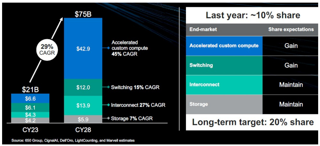
HBM: The Key Memory Technology Behind Generative AI
- Basic Structure and Advantages of HBM
HBM (High Bandwidth Memory) is built by stacking multiple DRAM dies on top of a logic die and connecting them through Through-Silicon Vias (TSVs). Its advantages include:
Ultra-high bandwidth: HBM provides TB/s-level memory bandwidth via a wide data bus—over 20× faster than conventional DDR. Because the memory stack is located close to the logic die rather than on a distant DIMM module, the data transmission distance is much shorter, significantly reducing latency and energy consumption.
Power and area efficiency: By stacking DRAM vertically beside the processor, HBM shortens data paths and achieves much higher memory capacity per unit area.
For each new generation of GPUs or ASICs, the critical performance improvement often comes from increased HBM capacity. For example, moving from Nvidia H100 to H200 or B200 to B300, the core count and frequency remain unchanged, but the HBM stack increases by 50 %, and the memory generation advances from HBM3 to HBM3E.
2.HBM Manufacturing and Competitive Landscape
Process differences:
SK hynix uses advancedMR-MUF(Molded Reflow Underfill) technology, filling the gaps between stacked dies with liquid epoxy molding compound at room temperature, which improves yield and thermal performance. SK hynix currently holds over 60 % of the HBM market.
In contrast, Samsung and Micron useTC-NCF(Thermo-Compression Non-Conductive Film), which requires 300 °C processing and higher pressure, increasing the risk of die warpage.
Process nodes and base dies:
HBM4 will use1b nm or 1c nm DRAMdies and4 nm logic base dies, which handle stack control, I/O interface management, and custom logic integration. If 1c nm development lags, SK hynix—with its 1b nm yield advantage—could further widen its lead.
Hybrid bonding:
Cu-Cu hybrid bondingenables sub-10 µm pitch, lower resistance, and improved thermal performance. However, the required equipment and cleanroom investments are extremely costly. Large-scale adoption is expected withHBM5 20-Hi stacks around 2028–2029.
China’s catch-up:
CXMT (ChangXin Memory Technologies) began HBM2 mass production in 2024 and is developing HBM3, with plans to launch HBM3E by 2027—shortening the technology gap to about four years.
- HBM Supply-Demand Outlook and Market Size
Supply and demand:
Global HBM demand is estimated at1,128.6 million GB in 2024and2,293.0 million GB in 2025, versus supply of1,068.1 million GBand2,210.9 million GB, leaving gaps of about5.4 %and3.6 %, respectively.
Shift to new generations:
HBM3/3E’s production share will jump from 33 % in 2023 to 81 % in 2024 and reach 89 % by 2025, signaling the rapid phase-out of older generations.
Nvidia and SK hynix signed apriority supply agreementfor HBM3E. Mass production of 12-high HBM3E started in Q3 2024, with first-generation 12-high HBM4 entering production in 2025.
Market scale:
TSMC’s CoWoS output in 2024 is around252,000 wafers, while global HBM demand is approximately40 million units, representing a market worthUS $9.14 billion. Nvidia accounts for 58 % of demand, Google TPU for 15 %, AMD for 14 %, and Chinese companies for about 7 %.
Why Cloud Service Providers Develop Their Own AI ASICs
Cloud service providers (CSPs) face two major cost pressures:
The high price of premium GPUs like the H100.
The massive power consumption required for large-scale model training and inference.
ASICsoffer a way out: by tailoring the hardware to specific workloads (e.g., matrix multiplication, tensor operations), they achieve higher performance-per-watt than GPUs.
Although North American cloud players’ AI ASICs typically offerlower peak compute than Nvidia’s H100, their cost and power advantages result in better overallperformance-per-dollar. For example,Google’s TPU v6andMicrosoft’s Maia 100reach90 % and 80 % of H100’s non-sparse performance, respectively.
Forinference, power, latency, and cost are decisive factors. CSET’s analysis shows that ASICs outperform CPUs by100–1000× in efficiencyfor inference tasks.
McKinsey forecasts that by 2025, ASICs will account for40 % of inferenceand50 % of training workloadsin data centers, indicating large-scale adoption of custom accelerators by major CSPs.
ASIC Growth Drives HBM Demand
Even though ASICs improve energy efficiency, theirhigh compute throughput still requires high-bandwidth memory. Chips like TPU and Maia typically integrate HBM stacks to achievemulti-TB/s bandwidth, paired with high-efficiency interconnects to minimize data stall time.
Companies likeMarvellare re-architectingHBM I/O and co-packaged optics (CPO)to reduce energy and support more stacked HBM per die. Their innovative design moves the HBM interface circuitry from the XPU die edge to thebase die under the stack, cuttingI/O power by 70 %and freeing25 % of die areafor additional compute units. This optimization boosts the number of HBM stacks per XPU by33 %, helping CSPs lower total cost of ownership.
Meanwhile, ASIC design houses such asAlchipandGUCare usingTSVs and hybrid bondingto build 3DIC solutions that further enhance thebandwidth and energy efficiencybetween compute dies and HBM. These technologies provide the infrastructure for CSPs tomassively deploy custom AI chips.
HBM Competitive Landscape and Supply Chain Evolution

In addition, theHBM supply chain spans five critical segments:
HBM IP,
Raw materials,
Die design,
Chip manufacturing
Packaging and testing.
Because HBM adopts a3D stacked structure, demand forupstream equipment—such asTSV (Through-Silicon Via) processing tools,wafer-level packaging equipment, andbonding machines—is rising rapidly.
On thematerials side, key elements includeEMC underfill compounds,composite molding materials, andTSV buffer layers. Major suppliers are buildingcompetitive barriersthroughpatent portfoliosandtight control over their supply chains, shaping the evolving competitive landscape of the HBM industry.
Key Takeaways
Memory wall and new interconnect technologies:
Current HBM relies on stacking and silicon interposers to deliver bandwidth, but this approach comes withhigh costs and thermal challenges. Future architectures may abstract memory usingphotonic interconnectsorCXL-based memory pooling, enabling efficient data sharing and distribution across multiple accelerators. It will be critical to examine the role ofCXL 2.0/3.0in AI data centers and the potential ofphotonic wiringto overcome“shoreline limitations.”
Hybrid bonding and back-end integration:
Hybrid bondingcan increase inter-layer interconnect density and is expected to be introduced in theHBM5 generation. However, its impact on cleanroom class requirements, wafer grinding equipment, and overall manufacturing cost still requires in-depth analysis.
Cerebras :Near-memory computing and HBM alternatives

Companies like Cerebras (wafer-scale processors) and Groq (near-memory architectures) use massive on-chip SRAM to minimize data movement. It’s worth exploring whether Processing-in-Memory (PIM) or Large Processing Units (LPU) could partially replace HBM in certain AI workloads.China’s HBM development and geopolitics: CXMT’s HBM program and China’s semiconductor self-sufficiency push could reshape global supply chains and pricing. Meanwhile, U.S. export controls and licensing restrictions add further uncertainty. How these geopolitical factors will affect the global HBM market remains a key question.

HBM and photonic packaging integration:
To improve energy efficiency, vendors are investigatingco-packaging HBM with photonic dies or CPO (Co-Packaged Optics). For example,Marvellhas proposed rearchitecting HBM I/O to integrate optical transceivers—potentially a major direction for thepost-HBM era.
Memory expansion protocols and software ecosystems:
Beyond hardware,compiler and framework support for HBM managementis crucial for GenAI workloads. It’s important to study howPyTorch 2.0,TensorFlow XLA, and other frameworks optimizeHBM paging and data pipelinesto fully exploit available bandwidth and capacity.
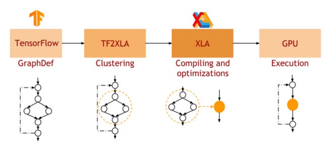
AI wave amplifies memory demand:Training and inference for large models are fundamentally constrained bymemory bandwidth and capacity, making HBM an indispensable component of AI accelerators.Upgrading to newer HBM generations or increasing stack heightscan significantly boost model throughput without changing compute power.
CSP custom silicon drives HBM demand:Cloud hyperscalers likeGoogleandMicrosoftare designing custom ASICs to optimize energy efficiency and cost, butstill rely on HBMto provide high-speed cache and bandwidth. The industry is exploringHBM I/O redesign and 3D IC integrationto reduce power and area overheads.
Evolving competitive dynamics: SK hynixcurrently leads the HBM market thanks to itspackaging technology and yield advantages.SamsungandMicronare working aggressively to catch up, whileChinese vendorsare accelerating their entry. Future competition will center onprocess nodes,packaging innovation,hybrid bonding, andphotonic interconnect technologies.

Emerging topics to watch:Breaking thememory wallwill requirenew interconnectandnear-memory computingtechnologies.Hybrid bonding,electro-optical packaging, andChina’s semiconductor policieswill also play critical roles in shaping the industry.
This synthesis aims to provide readers with a clear understanding of theinterplay between AI chips and HBM, as well asemerging trends that will define the next wave of memory innovation.
Summary of Explosive Growth of the HBM Market
- Surge in Production and Consumption
GPU shipments:1.638 million units in 2023 → 7.133 million units in 2027
ASIC shipments:2.556 million units → 6.949 million units
Average GPU memory usage:80 GB → 422 GB
Average ASIC memory usage:40 GB → 364 GB
- Market Size Expansion
The total HBM market is projected to skyrocket from$3 billion to $53 billion, with a97% CAGR.
Although unit prices will decline, the sharp increase in per-device capacity and adoption rates will massively expand the overall market size.
- Technology Node Transition: HBM4 / HBM4e
HBM4 will become mainstream starting in2026.
HBM4e will furtherboost bandwidth,increase stack height, andraise packaging integration complexity.
- DDR4 / DDR5: A Supply–Demand Inflection Point
DDR4 investments are gradually shrinking, and by 2026 a10–15% supply gapis expected.
The transition towardDDR5 and HBMis firmly underway, pushing DDR4 into alow-supply, structurally high-pricephase.
- HBM4 / HBM4e Process and Base Die Trends
By2028, demand forHBM4e base diesis projected to surpass80 million units.
HBM4 will use12 nm processes, while HBM4e will leverage5 nm nodes, underscoring thedeep integration between memory manufacturing and leading-edge logic foundries.
The memory industry is evolving from“component manufacturing” to “co-designed systems”, integrating SoC + memory + interposers + packaging.
This also signals asupply-chain power shift: HBM is no longer just a DRAM product but acore system componentthat determines performance and integration strategy.
DRAM equipment spending:expected to reach$32.7 billion in 2026, up 10% YoY.
NAND equipment spending:will surge in 2025 and remain strong in 2026 (9%–30% growth).
- Key technology drivers include:
Increased EUV layers (advanced nodes)
HBM4/4e packaging and testing
Wafer dicing and warpage control
High-k materials and thermal compression bonding
Introduction of mobile HBM (LLW DRAM)
These trends indicate thatequipment investment is shifting toward more advanced nodes and complex packaging, raising the technical barrier for market participants.
- NOR Flash: The “Hidden Demand Driver” for Edge AI
The NOR Flash market is tightening due topackaging capacity constraintsandthe explosion of IoT and Edge AI devices.
ByH1 2026, NOR supply shortages could reachmid-single-digit percentages.
Wearables, sensor modules, and automotive electronicswill push NOR prices higher, making it a strategically important but often overlooked segment of the memory market.
- Structural Characteristics of the New Memory Cycle
Unlike previous rebounds driven bysupply cuts, the current memory upcycle is fueled bystructural AI-driven demand growth.
Even if consumer markets remain weak in early 2026,AI demand will support pricing. A supply shortage is expected to last4–6 quarters, withserver DRAM and enterprise NAND spot marketsbecoming particularly tight.
Structural vs. Cyclical Cycles — Will AI Reshape the Traditional Memory Boom–Bust Pattern?
Traditional Cycles vs. the AI Shift
Historically, theDRAM/NAND memory industry has been highly cyclical, driven by end-market demand (e.g., PCs, smartphones) and inventory adjustments. These2–3 year “cyclical waves”typically follow a familiar pattern: when demand surges, suppliers expand capacity and prices rise; eventually, oversupply leads to sharp price declines.
However, with the rise ofArtificial Intelligence (AI), this classic cycle is beingreshaped by structural growth forces. Industry observers note that the current“supercycle” in memoryis fundamentally different from past inventory-led booms: demand is now beingdirectly pulled by AI compute workloads, lifting baseline consumption and creating a more durable, higher-value growth trajectory. In other words, AI isshifting memory demand from single-market cycles (e.g., PCs, mobile) toward multi-sector synchronized structural expansion.
Market Data and Forecast Models
Multiple market studies support the view thatfuture cycles will be longer and less volatile:
A U.S. investment bank report revealed thatOpenAI plans to consume up to 900,000 DRAM wafers per month by 2029, roughlyhalf of total global DRAM capacity in 2025. A single AI customer could support what used to be half of the entire industry — structurally lifting the demand baseline.
According toTrendForce, AI-driven demand has pushedglobal DRAM inventory turnover down to 3.3 weeks, aseven-year low, far below the historical norm of ~10 weeks — highlighting acute supply tightness.
UBS analystsproject that OpenAI’s in-house AI chips will useHBM memory, with a single project consuming500,000–600,000 DRAM wafers per month between 2026–2029.
OpenAI’s“Stargate” supercomputeralone is expected to consume900,000 DRAM wafers per month, equivalent to~40% of global supply— an unprecedented level of demand concentration.
At the same time, major DRAM vendors (Samsung, SK hynix, Micron) arepivoting part of their production to HBMandupgrading process nodes (e.g., 1c nm)to address AI-driven growth, as near-term capacity expansion is difficult.
Some executives even predict prolonged tightness:Phison CEO K.S. Puaforecastsa decade-long NAND undersupply starting 2026, whileMorgan Stanleybelieves DRAM price increases — fueled by AI demand — willcontinue through H1 2026, offsetting macro weakness.
Toward a Longer, Smoother Supercycle
Two forces are making thememory cycle longer and less volatile:
Strategic AI Data Center Demand:
DRAM/HBM and enterprise NAND consumption is increasingly tied tolong-term AI infrastructure investments, not short-term consumer electronics cycles. Thissmooths demand curves, reducing sudden drops.
Disciplined Supply Expansion:
After severe losses in the last downturn, memory makers are nowmore cautious with CapEx, expanding capacity more slowly. This keeps supply–demand healthier for longer.
Combined, these factors point to a“tight, high plateau” cycle, characterized bymoderate, sustained growthrather than the sharp boom–bust swings of the past.
For example, multiple forecasts point tomulti-year DRAM upcycles, withstructurally higher pricesdriven by AI adoption. Of course, risks remain: if AI growth slows or CapEx surges too quickly,cyclical corrections could still occur, but theiramplitude and frequency will likely be lowerthan in previous decades.
Strategic Implications for Memory Players
Memory companies shouldtreat this as a structural growth wave, not just another short-term upcycle. Strategic shifts include:
Move from short-term to long-term planning: Maintain disciplined capacity expansion during booms to avoid future oversupply.
Prioritize high-value products: Focus capacity onHBM and enterprise SSDs, which have higher margins and strategic importance for AI.
Use market modeling to plan ahead: Align capacity and raw material procurement with thefuture wafer demand of major AI customerslike OpenAI, locking in long-term contracts.
Collaborate with governments and industry: Build real-timeeconomic indicator systems(e.g., AI server shipments, cloud CapEx) to guide supply planning and inventory policies.
By adopting these strategies, the memory industry cancapitalize on the AI-driven supercyclewhileavoiding the boom–bust trapof previous decades — achievingsteady, high-value growth in the AI era.
HBM4e and Advanced Logic Process Competitiveness — Process Dependence and Strategic Collaboration in Next-Gen Memory
Dependence of HBM4/4e on Advanced Logic Nodes
The fourth generation of High Bandwidth Memory (HBM4/4e) is widely regarded as acritical enabler for the AI era, requiring significantly higher I/O interface width and speed. To achieve this, thebase diearchitecture of HBM has undergone a major technological shift.
In previous generations (HBM1–3), base dies were typically manufactured using DRAM fabs’in-house planar DRAM processes, serving mainly as passive signal pass-through layers. However, withHBM4, the data interface width hasdoubled from 1024 bits to 2048 bits, and per-pin data rates are approaching10 Gbps, exposing thespeed, signal integrity, and power limitationsof traditional DRAM processes.
To overcome these challenges,leading vendors (Samsung, SK hynix)have decided to moveHBM4 base die productiontoadvanced foundry logic nodes(e.g., 12 nm or even 5 nm FinFET). For instance,TSMChas announced support forN12FFC+ (12 nm)andN5 (5 nm)processes for HBM4 base die manufacturing. A 5 nm base die provideshigher logic densityandlower power consumption, ensuring stable control circuitry operation in ultra-high-speed environments.
As a result,HBM4/4e is deeply dependent on leading-edge logic processes, pulling the memory industry into an unprecedented“process race.”
Cost and Yield Challenges of 5 nm Base Dies
While moving to5 nmprocesses boosts performance, it also bringssignificant cost and yield challenges:
Cost Structure:
5 nm foundry wafers are extremely expensive, partly due to EUV lithography tools that cost$200–300 million per unit. Outsourcing the base die to advanced foundries significantly increases manufacturing costs. Industry reports indicate that thebase die accounts for ~20% of total HBM4 manufacturing costat TSMC, pushing up overall HBM pricing.
Recent market reports suggest thatSK hynix’s HBM4 pricing has risen ~70% over HBM3E, with12-Hi HBM4 stacks priced around $500 each, compared to ~$300 for HBM3E — largely reflecting the cost of advanced logic processes.
Yield Ramp:
Advanced nodes like 5 nm typically experience ayield learning curve. If base die yields are low, unit costs increase sharply and candrag down the overall stack yield, asany defective base or DRAM die causes the entire HBM stack to fail.
South Korean industry sources note that Samsung initially planned to use 8 EUV layers for its 1c DRAM node but reduced this to 6–7 layers to balance cost and yield. Similarly, achieving reasonable yields for 5 nm base dies is amajor challenge.
Samsung may absorb some costs through its own fabs, whileSK hynix and Micron must rely on TSMC, facing higher foundry prices. Micron evendelayed its adoption of advanced nodes to HBM4e, waiting for cost structures to stabilize.
Strategic Collaboration Models Between Foundries and Memory Vendors
To address these challenges, memory makers and foundries are enteringdeeper strategic collaborationsthan ever before. Key models include:
Foundry Alliances & Capacity Lock-Ins:
Micronhas formally partnered withTSMCto manufacture HBM4e base dies, targetingmass production in 2027. Micron essentially purchases advanced logic capacity and then packages the finished HBM at the wafer level. This guarantees Micron access to 5 nm/3 nm technology, while TSMC secures long-term capacity utilization — amutually beneficial lock-in.
Joint Development & Custom Design:
SK hynixsigned anMOU with TSMC in April 2023to co-develop HBM4, focusing on tighter integration between the base die and CoWoS packaging. Ajoint “One Team”R&D group works on optimizing base die performance, lowering power, and co-tuning the interface with TSMC’s advanced packaging.
Thisgoes beyond a pure foundry relationship, resemblingco-development, where the memory vendor provides HBM specs and TSMC contributes process and packaging expertise — enabling SK hynix to stay ahead in HBM4 performance while reinforcing TSMC’s role in the AI packaging ecosystem.
Vertical Integration:
Samsung Electronics, which operates both DRAM and foundry divisions, pursuesfull vertical integration. Its HBM4 base dies are produced in-house using 5 nm/4 nm lines, combined withI-Cube packagingtechnologies. This allows Samsung tocontrol costs and supply, avoiding reliance on rival foundries. However, it also bears thefull R&D and yield riskinternally, demanding strong technical capabilities.
Customer-Driven Customization:
Looking forward,customized HBM base dieswill become common. Major AI players likeNVIDIA and OpenAImay design their own base dies for HBM4e, then rely on memory vendors to stack DRAM and foundries for fabrication. Samsung plans to useVCS (Vertical Cu-Post Stack), while SK hynix is developingVFO (Vertical Fan-Out)packaging to support such customized workflows.
Thistri-party collaboration model— AI company + memory vendor + foundry — enables tailored HBM optimized for specific accelerators.
Strategic Implications
As HBM moves into theadvanced process era, memory vendors mustadopt flexible, multi-pronged strategiesto stay competitive:
Collaborative R&D:Early engagement with foundries (e.g., SK hynix + TSMC) can shorten the yield ramp and tailor processes to HBM requirements.
Cost-Sharing Agreements:Long-term capacity contracts with foundries can secure better pricing and transfer part of the cost to AI customers via pre-orders.
Vertical Integration & Customization:Vendors can either follow Samsung’s self-sufficiency model or build co-development capabilities with key customers.
Talent & Technology Roadmaps:Investing in 5 nm and below expertise, including3 nm and High-NA EUV, ensures leadership as logic-memory integration deepens.
Through such strategies, memory vendors canleverage advanced nodes while mitigating risks, positioning themselves strongly in theHBM4 era of AI memory competition.
Edge AI and Mobile HBM Technology – The Outlook for High-Bandwidth Memory in Smartphones, XR, and Automotive Devices
The Concept and Demand for Mobile HBM (LLW DRAM)
As AI applicationsexpand from the cloud to the edge, devices such assmartphones, AR/VR headsets (XR), andautomotive AI systemsare facing rapidly increasing demands forhigh-bandwidth, low-latency memory. Traditional mobile DRAM solutions likeLPDDR5Xoffer limited bandwidth and are no longer sufficient to handle the massive data throughput required foron-device AI inference.
To address this, the industry has proposed a “mobile version of HBM,” also referred to asLow Latency Wide I/O DRAM (LLW DRAM)orLPW DRAM. The core idea is towiden the memory I/O interface(i.e., implement a wide bus) whilelowering the per-channel speed, achieving bothhigh data transfer ratesandlow power consumption. In other words, this approach brings theHBM wide bus conceptto mobile devices but optimizes it forbattery-powered environments.
AtISSCC 2025, Samsung revealed its plan to launchnext-generation low-power wide I/O DRAM (LPW/LLW DRAM), with the first mobile products expected to debut in2028. Meanwhile, rumors suggestAppleis considering integrating mobile HBM technology into its20th-anniversary iPhone, slated for2027, to dramatically boost on-device AI capabilities.
This indicates that incorporatingHBM-class memoryinto smartphones, wearables, and automotive systems isno longer a distant vision, but rather a key industry focus for thenext 2–3 years.
Adoption Timeline and Thresholds
Thecommercialization window for mobile HBMis expected to fall between2026 and 2028. Major memory manufacturers such asSamsungandSK hynixare actively developing their respective LLW DRAM solutions. Samsung has publicly stated that it will release thefirst mobile device equipped with LPW DRAM in 2028.
Market rumors also suggest thatHuaweimay attempt tobeat Apple to market, potentially unveiling a flagship smartphone using HBM-like memory as early as2025–2026, although this has yet to be confirmed.
Based on current trajectories,around 2027is likely when leading vendors willpilot mobile HBMinultra-premium smartphonesorMR headsets, targeting use cases such ason-device LLM inferenceandreal-time computer vision.
In theautomotive domain, high-end autonomous driving platforms require extremely high memory bandwidth. Some are currently adoptingGDDR6, butnext-generation automotive AI chips (2027+)may turn tomobile HBMto achieve bothhigher bandwidthandlower power consumption. For example, future iterations ofTesla’s FSD chipsor other custom automotive accelerators may integrate mobile HBM as part of their architecture.
Overall, thekey barriersto mobile HBM adoption aretechnical maturityandcost absorption within flagship products. Both are expected to be gradually overcome toward theend of this product cycle, paving the way forwider deployment of mobile HBM between 2026 and 2028.
Breakthrough Conditions: Power, Packaging, and Cost
To bringHBM-class high-performance memoryintomobile and XR (Edge) devices, several technical bottlenecks must be overcome:
Power Consumption & Thermal Management
Mobile devices are strictly limited by battery capacity and compact form factors, making thepower overhead of high-bandwidth memorya key challenge.
LLW DRAM (Low-Latency Wide I/O DRAM)addresses this byincreasing the number of I/Os while lowering per-pin frequency, resulting in a large aggregate bandwidth withlower per-pin power. Samsung estimates that the new LPW DRAM candeliver over 200 GB/s bandwidth while reducing power consumption by ~54% compared to LPDDR5X.
As memory and SoC are tightly packaged, thermal density increases significantly. Advanced heat dissipation measures—such asvertical thermal channels,high-performance heat spreaders, orusing through-silicon copper posts in 3D packaging for heat conduction—are required. If power can be kept within acceptable limits and heat is effectively managed,mobile HBM becomes viable.
Packaging Technologies
Mobile devices cannot use thelarge silicon interposersfound in data-center GPUs due to size and cost constraints. To solve this, vendors are developingnew chip stacking and interconnection techniques:

Samsung VCS (Vertical Cu-Post Stack)andSK hynix VFO (Vertical Fan-Out)replace the large interposer withvertical copper pillars or fan-out packaging, tightly bonding wide-bus memory to the SoC.
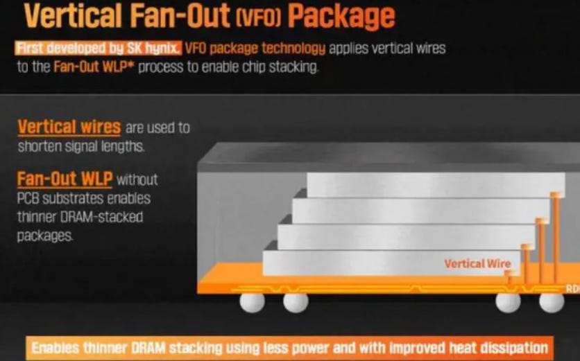
Samsung also proposedVertical Wire Bonding (VWB)at ISSCC, replacing traditional looping wires with straight vertical interconnects to reduce latency.

These are essentiallysimplified 2.5D/3D packaging methodsthat directly connect memory dies to processors through ultra-short interconnects. They enablewide I/O integration within a small footprintwhile maintaining manageable package height and reliability.
However,packaging yield is a critical challenge. Hundreds or even thousands of micro-interconnects must be bonded simultaneously and remain reliable over the device’s lifetime. This demandsprecise alignment,advanced materials, andprocess innovation. In short,mature packaging technology is a prerequisite for mobile HBM deployment.
Cost and Capacity
At current technology maturity,mobile HBM is significantly more expensive than LPDDR, both due toadvanced packagingand potentialsilicon stackingsteps. Itscost per bit may be several times that of LPDDR.
Analysts point out that mobile HBM facesthermal constraints and 3D stacking yield issuesin slim devices, further increasing costs. Commercial viability typically depends onmaturity, yield ramp-up, and scale effectsto bring costs down. Initially, mobile HBM will likely appear inultra-premium flagships or specialized devices, with prices expected to decline after2028as production scales.
Strategic Implications for the Edge AI Era
To prepare for theEdge AI boom, industry players shouldstart building mobile HBM capabilities early:
For memory vendors:
Invest inlow-power wide-I/O DRAM R&Dand collaborate closely with mobile SoC makers to define interface standards.
Considersmall-scale LLW DRAM pilot productionfor AI smartphones and AR glasses developer kits to accumulate real-world data and refine processes.
For device OEMs:
Evaluate theperformance gains vs. cost trade-offsof mobile HBM early.
Reserve board space and power budgetsin 2026–2027 flagship roadmaps to enable quick adoption once the technology matures.
For foundries & OSATs:
Expand advanced packaging capacityand build relevant engineering expertise in advance to support future mobile HBM orders at scale.
For industry alliances:
Collaborate onJEDEC or open interface standardsfor mobile HBM to foster a multi-vendor ecosystem, accelerate cost reduction through volume, and avoid vendor lock-in.
With these strategies in place, the industry will be well-positioned tocapitalize on the Edge AI wave, usingmobile HBMto meet the rapidly growing demand forhigh-bandwidth memory in intelligent edge devices.

Supply Chain Bottlenecks and Capacity Expansion — Key Factors in HBM / Advanced Memory Manufacturing
Advanced Packaging Capacity Bottlenecks:
For HBM and other advanced memory products, not only front-end wafer processing but also back-endtesting and packagingare critical to determining whether production can scale smoothly. At present, the most severe constraint isthe shortage of advanced packaging capacity for HBM.
HBM requires 2.5D silicon interposers—such as TSMC’s CoWoS technology—to integrate multiple DRAM stacks with processors. However, TSMC’s CoWoS capacity is limited. Since 2023, surging demand for AI chips has made CoWoS packaging thecentral bottleneckin the AI supply chain.
TSMC plans to expand CoWoS capacity to75,000 wafers per month in 2025, and to90,000–110,000 wafers per month by 2026—roughly double its 2023 level. But demand is rising even faster. Reports indicate that despite these expansions,cloud giants like Amazon and Microsoft are still facing multi-year delaysin securing AI chip packaging slots.
This “sweet bottleneck” is pushing the industry to acceleratenext-generation packaging technologies, such aspanel-level packaging (CoPoS), which TSMC aims to pilot in 2026 and mass-produce by 2028. By replacing silicon wafers with large panels, CoPoS can dramatically increase the number of chips packaged per batch.
Between 2026 and 2028, however, conventional CoWoS capacity is expected to remain tight, becoming theprimary limiting factorfor HBM volume ramp. For DRAM makers, even if wafer capacity is sufficient, lack of timely packaging services can stall shipments. As a result, many companies are exploringalternative solutions:
Samsungis ramping its in-houseI-Cubepackaging,
Inteland OSATs are collaborating onEMIBandFOLOBtechnologies,
all aimed at reducing dependency on TSMC.

2025年5月1日
Testing and Yield Challenges:
Thetesting stageis another often-overlooked bottleneck. HBM testing is far more complex than conventional DRAM, involving:
Known Good Die (KGD) screening for each die before stacking,
TSV electrical testing,
High-speed interface stress testing, and
Extensive burn-in at the package level.
Before dicing, each DRAM wafer undergoesprobe testingto identify good dies, which requires higher tester precision and throughput. Once stacked into HBM,packaged devices must undergo stress and burn-in teststo weed out latent defects.
Due to HBM’swide I/O and large capacity, testing each device is time-consuming, creating significant demand for ATE (Automated Test Equipment). Leading ATE vendors have flagged this surge:
Advantest noted during its 2024 financial briefing thatHBM testing capacity must be expanded,
It expects HBM-related tester shipments to rise significantly in the second half of the year as capacity improves.

2025年8月10日
If test equipment supply cannot keep pace, even completed HBM dies will face delays in validation and shipment, forming another bottleneck.
To support the expectedHBM ramp in 2026–2028, IDM and foundry players must:
Expand high-end tester fleets,
Adopt more efficient test flows, such as wafer-level burn-in to reduce post-packaging fallout, and
Strengthen yield management.

HBM stacks involvedozens of small dies, meaning that any error in the chain can sharply reduce yields. The supply chain must therefore invest inadvanced inspection tools—such as 3D X-ray and AOI (automated optical inspection)—and ensure sufficient capacity at these inspection nodes during peak production periods. Otherwise,inspection itself could become a new choke point.
In short,packaging and testingare emerging as critical determinants of HBM supply growth. Without parallel expansion of these back-end capabilities, even breakthroughs in DRAM fabrication won’t translate into real shipment capacity.

2025年9月25日
Materials and Process Equipment Bottlenecks in Memory Device
The manufacturing of advanced memory also depends on whether the supply of critical materials and specialized process equipment can keep up with capacity expansion. For example:
High-k dielectric materials:
To shrink DRAM capacitor size and improve charge retention, major DRAM makers began introducing high-k materials (e.g., HfO₂ hafnium oxide) as capacitor dielectrics starting at the 1α/1β nodes. High-k requires precise ALD (atomic layer deposition) processing, mostly provided by a limited set of suppliers (e.g., JSR in Japan, Applied Materials in the U.S.). If high-k materials are widely adopted in HBM and other high-end DRAM, the demand for these chemicals and ALD tools will surge. Because production of such materials is complex and supplier concentration is high, any tightening of material supply during the 2026–2028 ramp-up phase could disrupt wafer manufacturing. In addition, yield ramping for high-k processes takes time; early production runs may have lower yields, indirectly constraining output.
Materials challenges are not limited to DRAM. ABF substrates, silicon interposers, and high-density glass cores used in advanced packaging are also potential chokepoints. For example, ABF substrate capacity expansion typically takes over a year to build new facilities, and there are few short-term substitutes. If substrate supply is insufficient, HBM packaging schedules may be delayed, creating shipment bottlenecks.
Thermal Compression Bonding (TCB) and equipment:
As noted earlier, TCB is a critical process for accurately aligning and bonding memory dies onto interposers or substrates. TCB requires specialized tools to heat and press each die individually, making it relatively slow. SK hynix’s MR-MUF batch reflow process is more efficient, but it too requires dedicated molding materials and equipment. During the HBM capacity ramp, the availability of high-pin-count, high-precision bonding and reflow tools will be a key determinant of whether expansion can keep pace. If manufacturers and OSATs fail to procure enough TCB tools or vacuum reflow ovens by 2026, bottlenecks could form at the packaging stage.
Moreover, tuning these tools to mass-production standards takes time, and training skilled operators is another hurdle. These constraints are often underestimated but very real—for example, during the 2024 NVIDIA H100 boom, packaging lines experienced workforce and equipment shortages, forcing urgent recruitment and extra shifts. To avoid similar problems in 2026–2028, the supply chain must plan ahead for equipment and manpower needs.
Advanced lithography and other bottlenecks:
Although packaging and testing dominate the discussion, front-end challenges may also constrain output. Starting at the DRAM 1γ/1δ nodes, EUV lithography is being introduced; if ASML cannot deliver sufficient EUV tools on time, wafer output will be capped. Additionally, TSV (through-silicon via) etching and plating—key steps in HBM die fabrication—depend on deep etch and electroplating tools. Delays in the delivery or ramp-up of these specialized tools can limit capacity expansion, particularly for Chinese manufacturers who may face restrictions on acquiring the most advanced etch equipment, impacting their HBM yield and output.
Thus, the entire value chain must systematically examine capacity bottlenecks across all stages—including but not limited to packaging, testing, materials, and equipment—and address weak links to ensure smooth ramp-up.
Impact on 2026–2028 capacity ramp:
Packaging capacity is likely to be the first and most critical bottleneck; before new technologies are widely adopted, HBM volume growth may be limited by packaging line expansion speed. Testing equipment and processes are a secondary bottleneck: less severe than packaging, but still capable of slowing shipments if capacity isn’t expanded early. On the materials and process side, as long as suppliers coordinate effectively, increased stockpiling and capacity expansion can typically meet demand—but specific materials like ABF substrates or specialty gases pose notable risks.
Overall, while annual growth in HBM and advanced memory is expected to be high between 2026 and 2028, the degree of supply chain coordination will determine the actual output curve. Poor handling of bottlenecks could lead to “demand waiting on supply,” capping sales below expectations; conversely, coordinated expansion could enable the industry to meet explosive market demand more smoothly.
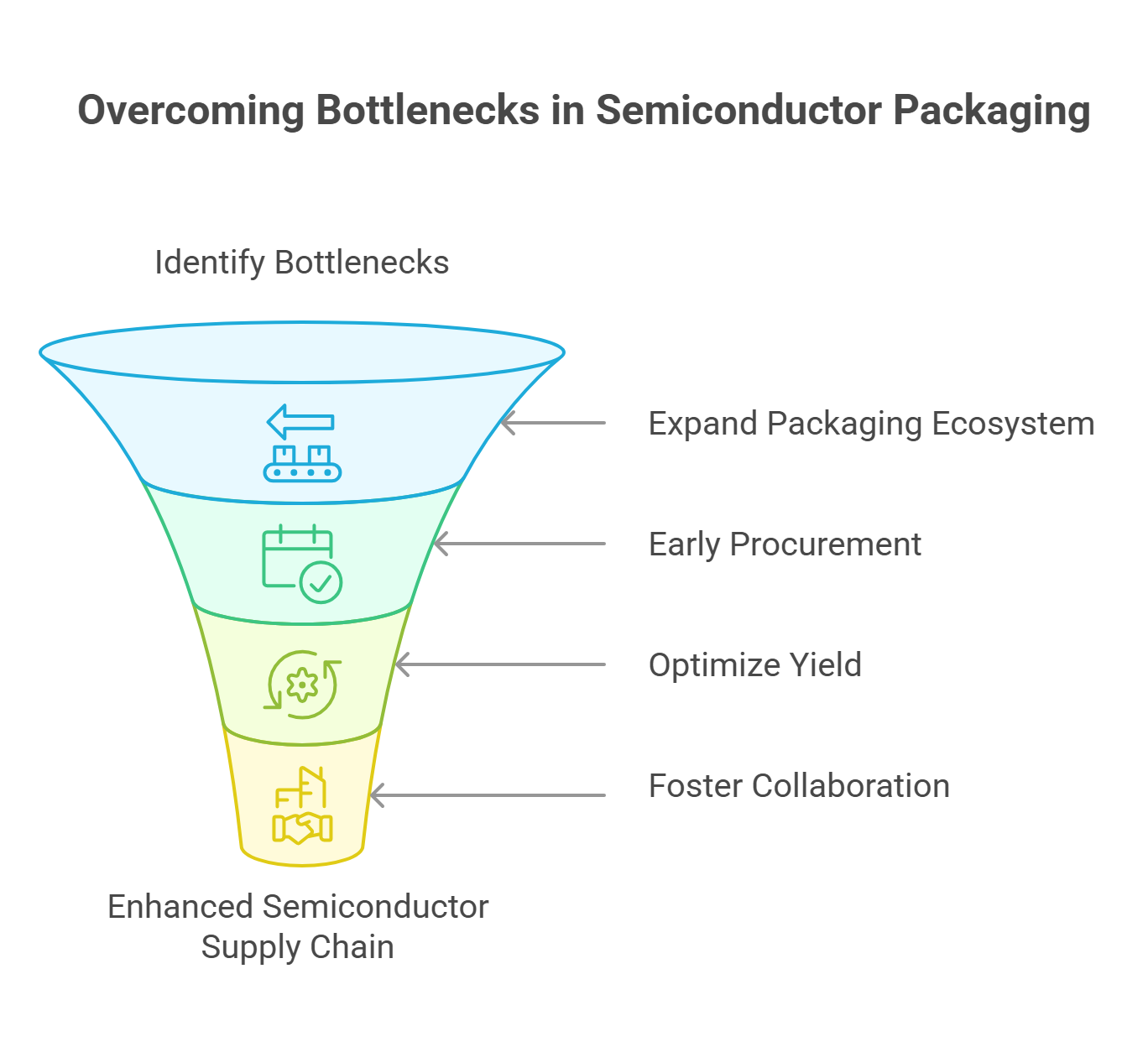
Strategies to overcome these bottlenecks:
Expand the packaging ecosystem:
Early procurement of equipment and materials:
For potential bottlenecks like test equipment, high-k materials, or ABF substrates, companies should place long-term orders 2–3 years in advance and build strategic inventories. For long lead-time equipment such as EUV scanners or ALD tools, CapEx planning must be meticulous to avoid last-minute shortages.
Yield and process optimization:
Companies can invest in more efficient testing methodologies (e.g., wafer-level burn-in, AI-assisted data analysis) to increase test throughput, and continue improving packaging processes such as adopting MR-MUF batch bonding to speed up assembly and improve yields. A 1% yield increase can translate into hundreds of millions of dollars in added output—well worth prioritizing.
Industry collaboration and government support:
Overcoming bottlenecks requires coordinated action across the ecosystem. Industry associations can organize supply chain summits to align capacity plans, while governments can offer tax incentives and fast-track permits for advanced packaging and testing expansions.
Through these measures, the memory industry can avoid local bottlenecks during the critical 2026–2028 window and fully convert technological breakthroughs into real market supply capacity, capitalizing on the AI boom rather than being constrained by it.
Materials and Process Innovations – Impact of New Technologies on Yield, Cost, and Capacity
EUV Adoption and Multi-Patterning:
Extreme ultraviolet lithography (EUV) represents a major innovation in advanced semiconductor manufacturing and is gradually being applied toDRAM production. The concept of “EUV layering” refers to using EUV lithography to pattern fine features that previously required multiple exposure steps with 193 nm ArF immersion, effectively increasing patterning density with fewer steps. For memory devices, this enablessmaller cell sizes(e.g., reduced 4F²) andhigher circuit density.

Attendees gathered at the event to commemorate the industry-first introduction of the High NA EUV system at the M16 fab
SK Hynix has been actively acquiring extreme ultraviolet (EUV) lithography machines from ASML to produce advanced chips. A 2021 contract involved a $4.3 billion investment over five years, and more recently, the company installed the industry’s first commercial High-NA EUV system at its M16 fab for memory production. SK Hynix is also reportedly planning to acquire about 20 additional EUV systems by 2027 to double its EUV capacity.
SK hynix Introduces Industry’s First Commercial High NA EUV
However, EUV introduces significantcost and yield challenges. On one hand, EUV scanners are extremely expensive — each tool costs roughly$200–300 million— and have relatively limited wafer throughput per hour. Adopting EUV thus requires a surge in upfront capital expenditure and fundamentally reshapes the manufacturing cost structure.
To control costs, companies likeSamsunghave reportedly sought toreduce the number of EUV layersin DRAM: for example, Samsung’s 1c DRAM node was initially planned to use 8–9 EUV layers but was later scaled back to 6–7 layers to save on equipment investment.
On the other hand,initial EUV yield tends to be low, due to factors such as mask defects and stochastic lithography errors. Overcoming these issues requires improvements inmask protection,pattern correction, and extensivepilot production data. As a result, during early adoption phases, DRAM yields may temporarily decline, raising per-chip costs.
In the long run, however, EUV simplifies the process flow byreducing multi-patterning stepsand their associated overlay errors, while improvingcritical dimension (CD) control, ultimately leading tohigher final yieldsandbetter performance consistency. Once yields ramp up and capital depreciation is amortized, theunit cost of EUV-patterned DRAM may actually fall, extending the scalability of Moore’s Law in the memory domain.
Overall, EUV represents a“high upfront cost, high long-term benefit”investment. Manufacturers must endure a period oflower yield and higher per-unit costduring the yield ramp phase, but once this transition is complete, they can reap significant benefits fromprocess simplification, improved pattern fidelity, and reduced overall costin advanced DRAM production.
Thermal Compression Bonding (TCB) and Advanced Stacking:
Innovations in thermal compression bonding (TCB) are having a significant impact on theyield and cost structureof HBM and other 3D-stacked memory technologies. Traditionally, to ensure precise alignment of each die, manufacturers have useddie-by-die thermal compression bonding, ensuring reliable fine-pitch micro-bump connections. However, this approach involves long process times and low equipment utilization, which drives up assembly costs and limits throughput.

A new generation of techniques, such aslarge-area simultaneous bonding(e.g., SK hynix’sMR-MUF process), enables multiple dies to be bonded in a single reflow step.
From acost perspective, MR-MUF eliminates the time-consuming die-by-die bonding steps, drastically increasing packaging throughput and lowering the per-unit assembly cost. While conventional TCB offers precision, it is expensive and scales poorly — costs rise sharply with each additional stack layer, making it unsustainable for future high-volume production.
Looking forward, if thermal compression bonding continues to evolve towardbatch and automated processing— for example, bonding multiple HBM stacks across an entire wafer in a single thermal compression step — it could massively boost packaging capacity and reduce packaging’s share of the overall cost structure.
This hasdirect implications for capacity planning: manufacturers that adopt high-throughput bonding technologies will require fewer packaging lines and less manpower, enabling them to deploy more capacity within limited fab space to meet peak demand. In contrast, companies that remain dependent on traditional TCB methods may facepackaging becoming a production bottleneck.
In short,innovations in thermal compression bondingoffer the dual benefits ofhigher yield per unitandlower assembly costs, making them an inevitable trend for next-generation advanced memory.
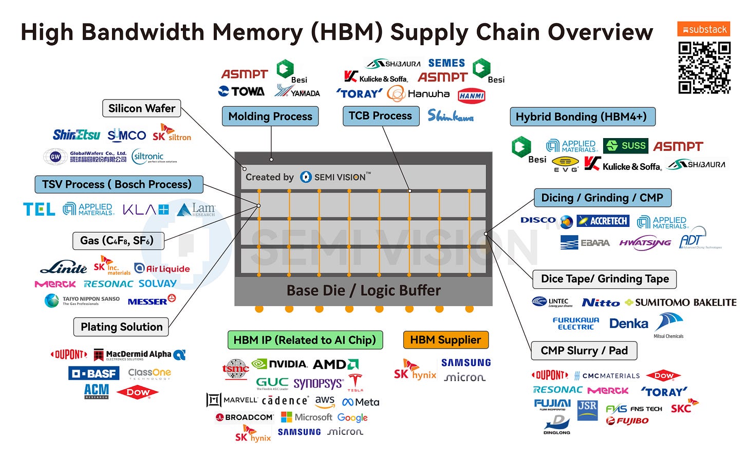
5 nm Base Die and Logic Packaging Innovations:
As discussed earlier in the HBM section, the introduction of 5 nm base dies (logic dies) has enabled a major leap in HBM performance, but it also brings significant implications for yield and cost structures. Each HBM stack now includes a base die containing several billion transistors—essentially a small SoC—whose yield directly determines the overall product yield.
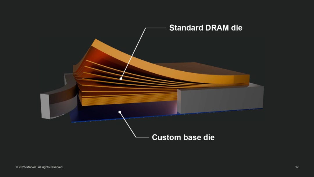
If initial 5 nm yields are only around 50%, half of the base dies would be scrapped. Combined with potential DRAM stack losses, the final product yield could be even lower. This presents a substantial supply challenge for HBM in 2025–2026. As a result, memory vendors and foundries must work closely to improve base die yields through strategies such as optimizing EDA fault-tolerant design, applying more relaxed design rules than those used for logic SoCs to trade performance for yield, or even performing localized wafer-level repair where technology allows.
Every 1% yield improvement translates into thousands of additional HBM stacks—an enormous economic gain that the industry is increasingly aware of. From a cost perspective, the base die accounts for roughly 20% of total HBM cost. Higher yields are essential to lower the per-unit cost.
Different collaboration models will also impact cost structures. For example, if companies like OpenAI or NVIDIA design their own base dies and outsource manufacturing, economies of scale could lower costs, but heavy customization may make capacity sharing difficult, potentially requiring higher prices to offset inefficiencies.
On the capacity side, 5 nm production is already in high demand among multiple customers. Memory makers must secure capacity agreements with foundries to ensure stable base die supply and avoid being squeezed out by CPU or GPU orders during peak periods.
There are also technical roadmaps exploringHBM without a base die, such as distributing logic functions within the DRAM layers or integrating them into the underlying interposer. If successful, this could simplify manufacturing and eliminate one 5 nm die, improving both yield and cost. However, in the near term, 5 nm base dies will remain mainstream.
Therefore, rapidly climbing the yield learning curve and driving down costs will be critical priorities for HBM suppliers around 2025.

High-k Dielectrics and Other Process Innovations
The use ofhigh-k materials in DRAM capacitorsrepresents a major technological breakthrough. Micron was the first to commercialize high-k capacitors at the 1α node, enabling cell capacitance to be maintained even as feature sizes shrank. This had direct implications foryield and reliability: high-k dielectric layers are thinner and exhibit more complex dielectric behavior, which can initially lead to higher leakage currents and increased variability, requiring extensive process tuning. In fact, Micron’s initial yield issues during early 1α ramp-up were closely tied to the challenges of integrating new materials.
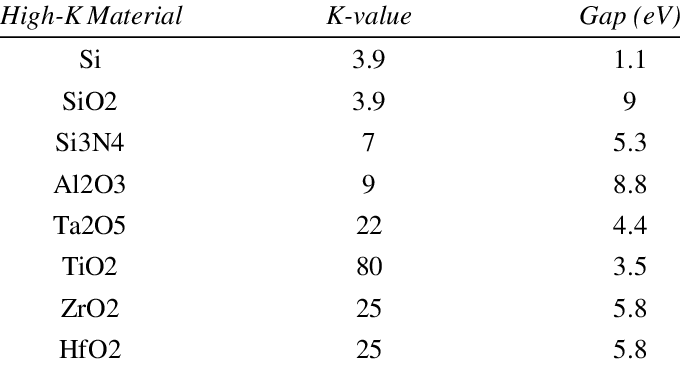
However, after iterative refinements, high-k capacitors ultimatelyimproved product reliability, since maintaining sufficient capacitance ensured longer data retention times.
From acost structureperspective, adopting high-k involves adding several ALD deposition and annealing steps. While these increase process complexity, they represent a small fraction of total DRAM manufacturing cost. In the long run, high-k enables greater scaling and cell density without needing larger cells or complex 3D structures, therebylowering the cost per bit. In the short term, however, R&D expenses rise due to new equipment purchases and materials development.
On thecapacity side, ALD processes are slower than conventional CVD, which could become a throughput bottleneck if equipment is not scaled up. In practice, manufacturers typically deploy multiple tools in parallel and optimize deposition cycle times to maintain line cadence. Thus, while high-k is a new technology,capacity challenges can be managed through equipment scaling.
Other Process Innovations
EUV in 3D NAND: As 3D NAND surpasses 200 layers, traditional 193 nm lithography requires multiple patterning to form high-aspect-ratio staircase holes. Early signs suggest EUV may be adopted to improve pattern fidelity and alignment, potentially reducing overlay errors and rework rates—benefiting both yield and cost.
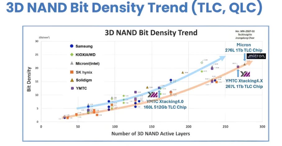
Direct and hybrid bonding: These advanced packaging methods eliminate micro-bumps and allow direct chip-to-chip connection, lowering interconnect impedance and increasing bandwidth. However, they requireextremely tight surface planarity and alignment control, making yield critical. If successful, hybrid bonding can simplify HBM interconnects and improve both yield and performance—but if poorly controlled, it can introduce new defects.
Overall, every new material or process innovation introducesshort-term variability and yield risk, but offers significant long-term performance and cost advantages once stabilized.
Overall Impact and Conclusions
Materials and process innovations act as adouble-edged sword: in the short term, they often cause yield drops and cost increases; in the long run, they enable better performance-to-cost ratios and expand production capacity limits. Companies must balanceyield, cost, and capacitycarefully.
In the AI era,standing still means falling behind—adopting new technologies is risky but inevitable. A smart strategy involvessmall-scale pilot runs and rapid iteration: introduce new processes on select lines, surface problems quickly, fix them rapidly, and gradually expand deployment. Close collaboration with the supply chain—especially materials and equipment vendors—is crucial for stable ramp-up and fast feedback cycles. Once stabilized, these innovations yieldhigher yields, lower cost per bit, and more flexible capacity, enabling the industry to meet AI’s massive memory demands in the coming decade.
Risk Management and Road-Mapping for New Process Technologies
Parallel R&D and manufacturing: Engage manufacturing teams early during R&D to ensure new processes consider yield and cost. Use pilot lines to validate EUV and hybrid bonding feasibility, and establishyield KPI triggersto drive structured improvements if early yields fall below targets.
Cross-domain collaboration: New materials and equipment often involve external partners. Formjoint teams with lithography and materials suppliersto address EUV yield issues, or work with packaging houses to co-optimize hybrid bonding. Data sharing accelerates problem-solving and shortens ramp time.
Phased cost modeling: Build cost projections for each innovation—short-term investment vs. expected cost crossover point—to plan deployment pace. For example, apply high-k first to high-capacity products to amortize costs; ramp EUV tools gradually based on learning curves.
Talent and IP accumulation: New technologies require new expertise. Companies should build in-house teams for EUV lithography, 3D packaging, and materials science while strengthening IP portfolios. Mastering these technologies early ensuresfuture market powerand protects against easy replication by competitors.
Strategic Implications for the AI Era
Under the wave of EUV, multi-stacking, advanced packaging, and high-k innovation, early adopters must be ready forinitial turbulencebut can gain long-term strategic advantage. Through careful planning and rapid optimization, companies canturn new technologies into competitive weapons, achieving yield improvement, cost optimization, and large-scale capacity expansion—fueling the AI economy of the next decade.
TheAI chip industry is undergoing an irreversible power realignment. The GPU-centric, single-vendor supply chain is fragmenting, giving way to a new landscape driven byOpenAI, custom ASICs, diverse HBM sourcing, and advanced packaging. HBM is no longer a mere auxiliary memory but astrategic assetinfluencing chip design, packaging capacity, supply chain configuration, and geopolitics.
Samsung and SK hynix, by controlling memory capacity and technology cadence, are becomingcritical nodesin the future AI ecosystem. TSMC and OSATs secure their positions through advanced packaging integration. While NVIDIA remains ahead, itsoverwhelming grip on the industry is loosening.
2026 will mark a structural turning point, shifting the AI supply chain from a “GPU economy” to an “ASIC × HBM economy.” Memory, packaging, power, interconnect, and capacity allocation will become the key battlefields over the next five years. Whoever controlspricing power in this supply chain realignmentwill dominate the next AI supercycle.
This is not merely a technological race—it is astrategic, financial, and geopolitical contest.


PreviousNext
TopLatestDiscussions







See all