TSMC x Nvidia : Breaking the Thermal Wall: How Advanced Cooling Is Powering the Future of Computing
TSMC x Nvidia : Breaking the Thermal Wall: How Advanced Cooling Is Powering the Future of Computing
- Source: SemiVision
- Author: SEMIVISION
- Published: 2025-10-05T21:08:34+08:00
- URL: https://tspasemiconductor.substack.com/p/tsmc-x-nvidia-breaking-the-thermal TSMC x Nvidia : Breaking the Thermal Wall: How Advanced Cooling Is Powering the Future of Computing


TSMC x Nvidia : Breaking the Thermal Wall: How Advanced Cooling Is Powering the Future of Computing
Original Article by SemiVision Research (TSMC, NVIDIA, Coherent, Jentech, AVC, Auras, Cooler Master, Mikros Technologies, Inspur, Invek, Ningbo Jingda, Fabric8Labs, Intel , xMEMS)

Oct 05, 2025
∙ Paid

The development of AI chips is fundamentally driven by the pursuit of higher performance, but this also brings a critical challenge: thermal management. Effectively dissipating the enormous heat generated by rising power consumption has become a key design consideration for next-generation AI chip architectures.
On the system level, the integration of optical engines is widely viewed as the future solution to overcome high-bandwidth interconnect bottlenecks. However, optical signals are highly sensitive to temperature fluctuations—even slight deviations can lead to transmission loss and degraded performance. This is why TSMC has adopted the Microring Modulator (MRM) approach, but MRM itself has strict thermal operating requirements. As a result, companies like TSMC and NVIDIA are actively exploring next-generation cooling technologies to meet these thermal demands.
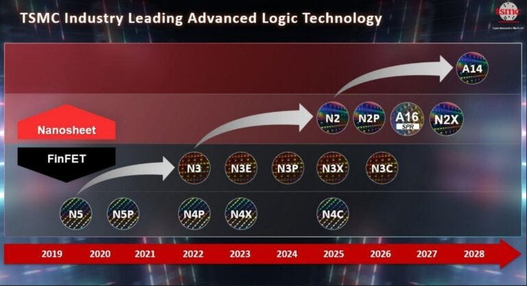
On the logic process side, TSMC’s evolution from N3 → N2 → A16 involves more than geometric scaling—it represents a transistor architecture transition: from FinFET, to GAA (Gate-All-Around), and finally to the Super Power Rail architecture in the A16 generation. This series of changes is aimed at achieving the optimal balance of PPA (Power, Performance, and Area), laying the foundation for high-efficiency AI computing.
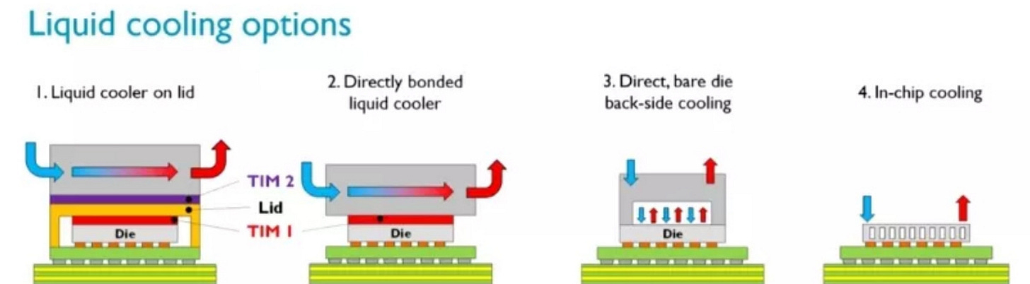
However, from a packaging and materials perspective, new challenges emerge. Traditional cooling depends on TIM (Thermal Interface Materials), whose material selection is limited, and thermal reliability is constrained within specific temperature ranges. To address this, TSMC has proposed an innovative Direct Liquid Cooling (DLC) solution. By applying a backside copper pillar process, TSMC integrates microfluidic structures directly into the backside of the chip, allowing heat to be removed through direct liquid convection, dramatically increasing cooling efficiency.
Nevertheless, since no-TIM architectures are not yet fully mature, the industry currently relies on heat conduction through the top lid of the package for thermal management. This has led to the emergence of the Microchannel Lid (MCL) concept—micro-channels are etched directly into the internal surface of the package lid, combined with liquid cooling. MCL is expected to serve as a critical transitional solution before full backside liquid cooling becomes mainstream.
SemiVisionbelieves that current AI chip logic process designs are almost exclusively carried out under high-density (HD) conditions. While this design approach significantly boosts computational performance per unit area, it also results in extremely high power density and heat flux, creating new thermal management bottlenecks.
A key question arises: Can the heat generated inside the AI chip be fully and evenly transferred to the package lid?
The internal thermal path of a chip involves multiple layers — silicon substrate, metal interconnects, micro-bumps, underfill, thermal interface materials (TIM), and more. Because of theselayered thermal interfaces, heat cannot be transferred 100% efficiently to the lid, leading tolocalized “hotspots.”This cumulative thermal resistance is one of the primary factorslimiting the chip’s maximum power output.
Improving Thermal Conduction Efficiency
The first key lies inshortening the thermal pathandreducing interfacial thermal resistanceat each layer, combined with introducinghigh thermal conductivity materials, such as:
Diamond thin films / CVD diamond
SiC substrates
Diamond Thin Film / CVD Diamond
Cu–diamond composites
These materials can dramatically increase the overall heat transfer coefficient.
Expanding Effective Heat Dissipation Area
The second key isincreasing the effective surface area for heat exchange— enhancingconvective heat transferthrough larger fluid–solid contact areas. This has led the industry to explore several promising solutions:
(1) Microchannel Cold Plate (MCLP)
Approach:Etching micron-scale channels into copper or silicon substrates, with coolant flowing directly near the chip.
Advantages:Maximizes surface-to-volume ratio; significantly lowers thermal resistance.
Challenges:High pressure drop, clogging risk, and increased pump power consumption.
(2) SiC Substrate as Heat Sink
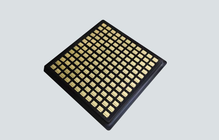
Material:Silicon carbide (SiC) has a high thermal conductivity of ~370–490 W/m·K, excellent mechanical strength, and high voltage tolerance.
Application:As a heat-spreading base substrate, it improves boththermal diffusionandmechanical/electrical performance, making it suitable for future>1 kW/cm²AI chips.
(3) Diamond Thin Film / CVD Diamond
Thermal Conductivity:1000–2200 W/m·K — far surpassing silicon (~150 W/m·K) and SiC.
Application:Used as aheat-spreading interlayerorcoating, directly deposited on chip or package surfaces.
Advantages:Ultra-low thermal resistance, nearly instantaneous hotspot dispersion; ideal for>500 W/cm²heat flux scenarios.
Challenges:High cost, complex CVD processes, and thermal expansion (CTE) mismatch with copper or SiC.
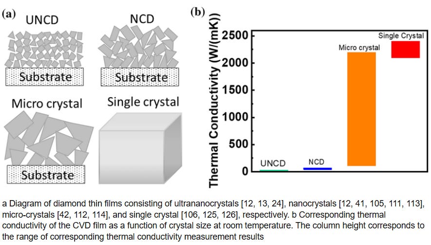
UNCD (Ultrananocrystalline Diamond)– composed of extremely fine grains on the nanometer scale.
NCD (Nanocrystalline Diamond)– slightly larger grain size than UNCD but still nanometer-scale.
Microcrystalline Diamond– composed of much larger grains, typically in the micron range.
Single-Crystal Diamond– a monolithic, defect-free structure without grain boundaries.
UNCD and NCD exhibitvery low thermal conductivity, close to that of conventional semiconductors, due to extensive grain boundary scattering of phonons.
Microcrystalline diamond shows adramatic increase, reaching values in the2000–2200 W/m·K range, as larger crystal sizes reduce boundary scattering and improve phonon transport.
Single-crystal diamond exhibits thehighest thermal conductivity, approaching2500 W/m·K, making it one of the most thermally conductive materials known.
This clear correlation between crystal size and thermal performance is critical for selecting diamond materials for high-power electronic cooling. Microcrystalline and single-crystal diamonds are particularly promising for next-generation AI/HPC chip heat spreaders.
(4)Cu–diamond composites

Diamond/Cu composite thermal management approach demonstrates outstanding potential for next-generation high-power electronic cooling. By incorporating Ti-coated diamond particles into a copper matrix using liquid–solid separation technology, the composite achieves exceptionally high thermal conductivity while maintaining strong interfacial bonding. The formation of a thin TiC interfacial layer plays a crucial role, significantly reducing interfacial thermal resistance and enabling efficient heat transfer between the diamond particles and the Cu matrix. With a measured TC of 457 W/m·K, and a theoretical potential exceeding 600 W/m·K at optimized coating thickness, this method offers a lightweight, mechanically robust, and thermally superior alternative to conventional heat spreaders. Its tunable structure through precise control of coating thickness and volume fraction makes it highly adaptable for AI/HPC chips, power devices, and advanced packaging platforms, where efficient heat dissipation is critical for stable, high-density operation.
TSMC and NVIDIA: Divergent but Complementary Strategies
TSMCfocuses onevolving TIM,silicon-integrated microfluidics, and introducingSiC/diamond substrates, pushing the boundaries ofmaterials and advanced packaging.
NVIDIAemphasizesMLCP,system-level liquid cooling(Direct-to-Chip and Direct-to-Silicon), andco-designing thermal and packaging architectures.
The Ultimate Goal
Both companies are converging on the same objectives:
Reduce thermal resistance
Increase effective heat dissipation area
Enable stable operation of future AI chips at higher power levels and higher densities
This thermal management evolution is becoming as critical as logic scaling itself in the AI computing era.

With the explosive growth ofgenerative AIandhigh-performance computing (HPC), both chip power consumption and heat flux density are rising sharply. The thermal design power (TDP) of a single GPU or AI accelerator has already surpassed thekilowatt level, and is advancing toward the3,000–5,000 W range.
While traditionalair coolingandcold plate liquid coolingcan delay thermal runaway, they struggle to cope with heat flux densities reaching as high as800–1,000 W/cm². Against this backdrop,microchannel liquid coolinghas become a new industry focus. By usingmicron-scale channel structures, it dramatically increases heat transfer surface area and fluid disturbance, achieving anunprecedented level of cooling efficiency.
For NVIDIA, sustaining energy-efficiency leadership in the next generation of AI GPU clusters means that thermal management has become just as critical a bottleneck as architecture design. As NVIDIA’s primary partner in advanced process technology and advanced packaging, TSMC is actively introducing microchannel liquid cooling into its 3DFabric platform (CoWoS, SoIC, etc.), exploring the possibilities of “in-package direct liquid cooling” and “chip-level direct cooling.”
This not only reflects TSMC’s view of cooling as a core component of Design-Technology Co-Optimization (DTCO/STCO), but also signals a paradigm shift in which thermal solutions will move from the system level down into the chip and packaging level, tightly integrated with process, packaging, and interconnect technologies.
As a result, the collaboration between TSMC and NVIDIA goes beyond process and compute—it is also evolving into a strategic alliance on thermal technology. With their joint push, microchannel cooling could become a defining inflection point in the AI chip era—reshaping the foundations of data center cooling infrastructure and potentially determining who can maintain leadership in the AI compute race.
As AI chip power consumption surges beyond2,000 Wand approaches5,000 W, traditional air cooling and cold-plate solutions are no longer sufficient. How to efficiently dissipate multi-kilowatt heat flux within limited space is rapidly becoming the defining factor that separates leaders from followers in next-generationHPC and AI infrastructure.
In thispremium feature report, SemiVision provides a comprehensive deep dive into:
Material Evolution
From traditional silicon substrates toSiC (Silicon Carbide),CVD diamond films, andCu–Diamond composite materials—we analyze thermal conductivity advantages, integration challenges, and package-level compatibility.
The Four Stages of TIM (Thermal Interface Material) Evolution
Fromthermal grease → phase-change materials → metal solder → nanoscale direct bonding, we explore how the industry is progressively approaching the goal of“zero-interface” thermal resistance.
Breakthroughs in Microfluidic Cooling Technologies
MCL (Micro-Channel Lid)andMLCP (Micro-Channel Liquid Cooling Plate): technical paths, yield bottlenecks, and package-level reliability verification.
Two-phase flowandCritical Heat Flux (CHF)management, with optimized pressure-drop designs for large-scale integration.
Comparative analysis oflaser machining, nano-etching, and 3D printingprocesses applied to copper, silicon, and SiC substrates.
Supply Chain Landscape
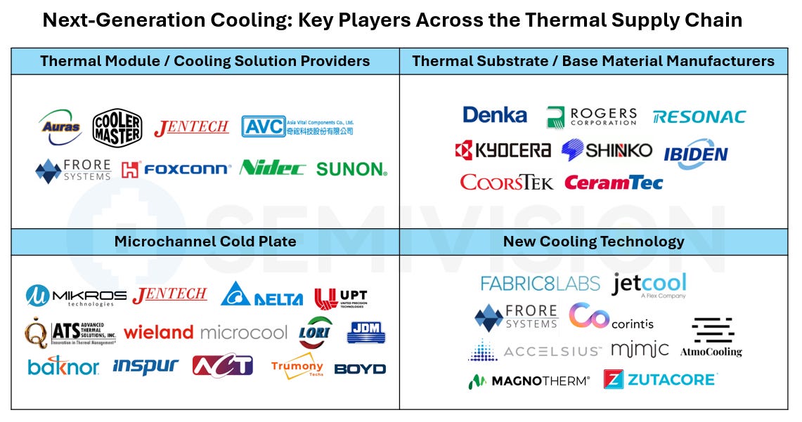
FromTaiwan’s four major thermal solution providers(Jentech, AVC, Auras, and Cooler Master) toChina’s Inspur/Invek and Ningbo Jingda, and emerging innovators such asFabric8Labs (ECAM technology)andxMEMS (µCooling active micro-cooling)—we assess who might take the lead in capturing this$5 billion next-generation cooling market.
Industry Trends
Why the NVIDIA Rubin generation is driving MLCP to become the new standard, and how TSMC’s 3DFabric platform is integrating direct liquid cooling, opening a new era of DTCO/STCO convergence across thermal management, packaging, power delivery, and optical interconnects.
These in-depth analyses reveal that AI thermal management is not merely an engineering challenge—but the new battlefield defining competitiveness across the semiconductor industry.
For Paid Members ,SemiVision will discuss topics on
Evolution of TIM Materials
SiC Substrates as a Future Concept for Microchannel Cooling
Thermal Management Technologies: Development and Future Trends
Vapor Chamber Lid (VC Lid)
Micro-Channel Lid (MCL)
More Advanced: Silicon-Integrated Micro-Coolers
System-Level Thermal Technologies in thermal management
Manufacturing Technology and Barriers
Core Concept of MLCP (Micro-Channel Liquid Cooling Plate)
Current MLCP Technology Progress and Challenges ( AVC & Auras & Cooler Master & JENTECH )
Why Microchannels Enable Much Higher Heat Flux Density per Unit Area
The Impact of Pressure Drop and Flow Distribution Inside Microchannels on Overall Cooling Performance
Heat Flux Density Supported by Microchannel Cooling in AI/HPC Chip Applications
Common Microchannel Fabrication Techniques: Advantages and Disadvantages
Machining Challenges for Different Materials (Silicon, Copper, SiC, Ceramics)
Methods to Ensure Geometric Accuracy and Surface Roughness of Microchannels During Fabrication
Addressing Interface Material and Reliability Issues in Direct-to-Chip Bonding of Microchannels
Will Microchannel Cooling Replace Traditional Cold Plates and Vapor Chambers as the Mainstream AI Chip Thermal Solution?
Microfluidic Cooling vs. Refrigerant-Based Direct Liquid Cooling — Which Is More Likely to Scale Commercially?
Will Microchannels Be Combined with Silicon Photonics (SiPh) or Co-Packaged Optics (CPO/OIO) to Provide an Integrated Thermal–Optical Platform?
Innovations Required for Microchannels to Handle 5000 W+ AI Chips (e.g., PCM Integration, Two-Phase Flow Control, Smart Monitoring)
Technological Breakthroughs and Industrialization Challenges of Microchannel Liquid Cold Plates (MLCP) in the AI Era
Demand Driven by NVIDIA: From Rubin to Rubin Ultra
Performance Leap: From Classical Models to Breakthrough Structures
Market Scale and Penetration: Liquid Cooling Becoming Mainstream
Supply Chain Landscape: From Thermal Vendors to System Integrators
Manufacturing Breakthroughs: Metal 3D Printing and Precision Sealing
Investment Opportunities and Key Components: From UQD to 3D Printing
From Technical Savior to Industry Standard
Fabric8Labs Shines at HOT CHIPS 2025
Why ECAM is Particularly Suitable for AI Thermal Management
Fabric8Labs:“ECAM Enabled Thermal Solutions for the AI Data Center”
Microchannel Cooling Innovation: From Machining to ECAM
Another cooling solution… xMEMS?
xMEMS µCooling / Fan-on-a-Chip Thermal Solutions
Evolution of TIM Materials
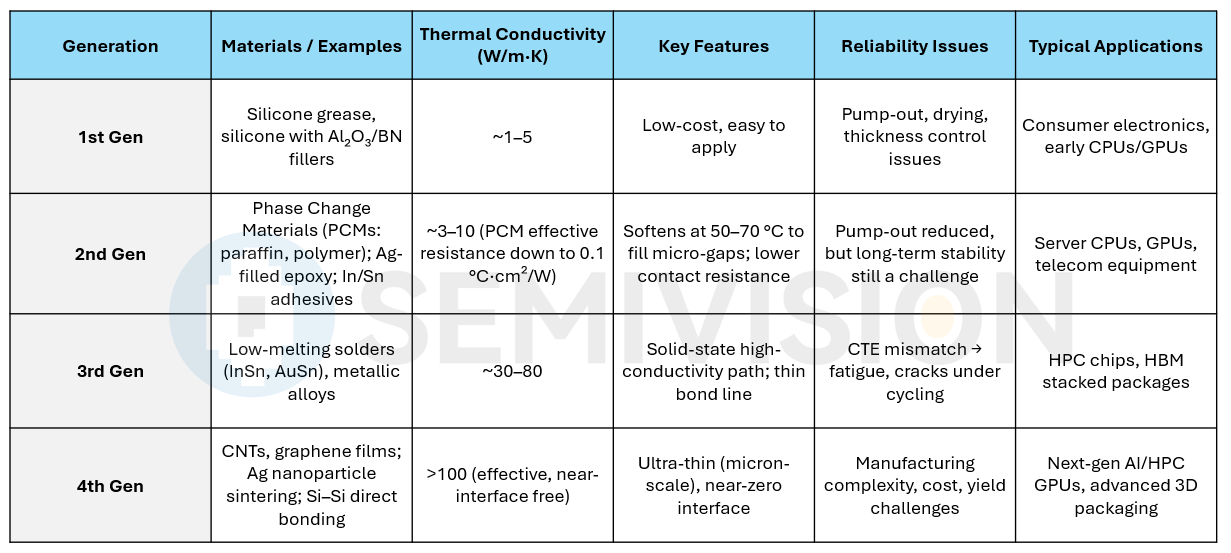
In high-power chip thermal design,Thermal Interface Materials (TIMs)serve as the critical “heat conduction bridge.” Over the past two decades, TIM development has primarily focused on two directions:improving thermal conductivityandenhancing interfacial reliability.
First Generation TIMs: Conventional Thermal Grease / Silicone Grease
Early solutions commonly usedsilicone-based thermal greasesor silicone filled withaluminum oxide (Al₂O₃) or boron nitride (BN).
Thermal conductivity was typically around1–5 W/m·K.
While inexpensive, they suffered fromthickness control issuesand long-term reliability problems such aspump-outand cracking.
Second Generation TIMs: Phase Change Materials (PCMs) and Metal-Filled Adhesives
To reduce thickness and thermal resistance, the industry adoptedhigh-conductivity PCMs(e.g., paraffin or polymer-based), which soften at50–70 °Cto fill micro-gaps, lowering contact resistance to the0.1 °C·cm²/W range.
In parallel,silver-filled epoxiesandindium/tin (In/Sn) metal adhesivesbegan to be used in high-end server CPUs and GPUs.
Third Generation TIMs: Metallic Solders and Alloy Interfaces
The next step involvedlow-melting-point metallic solders(e.g., InSn, AuSn), enablingsolid-state, high-conductivity connectionswith thermal conductivity in the30–80 W/m·K range.
These TIMs are now widely used inHPC chips and HBM stacked packaging, though they face challenges fromCTE mismatchleading to fatigue and cracking.
Fourth Generation TIMs: Nanostructures and Direct Bonding
Current research focuses onnano-carbon materials(CNTs, graphene),metal nanoparticle sintering(e.g., Ag-sintering), andSi–Si direct bonding.
These approaches can reduce TIM thickness to themicron scale, approaching the ideal of a “near-interface-free” connection, withsignificantly lower thermal resistance.

2025年7月22日

2025年7月28日
SiC Substrates as a Future Concept for Microchannel Cooling
AsAI chip power consumption surpasses 3,000–5,000 W, traditionalTIM + Cu/Si microchannelsolutions may no longer be sufficient. In this context, the introduction ofsilicon carbide (SiC) substratesis emerging as a promising next-generation direction:
Superior Thermal Conductivity
Single-crystalSiC has a thermal conductivity of up to 490 W/m·K—three times higher than silicon and about half that of diamond. This means that using SiC as a microchannel substrate could deliversignificantly better heat dissipation performancethan conventional silicon or copper channels.
Structural and Reliability Advantages
Thecoefficient of thermal expansion (CTE)of SiC is close to that of silicon, reducing interfacial stress and making it suitable fordirect bonding with chips or interposers. Compared with copper substrates, SiC is less prone to packaging fatigue caused by CTE mismatch.
Potential for Direct Liquid Cooling
By usinglaser drilling or deep etchingto form microchannels within the SiC substrate anddirectly bonding it to the backside of AI chips, it is possible to achievepackage-level direct liquid cooling. Such a structure couldcut thermal resistance to less than half of traditional solutions, even without TIM or with only an ultra-thin solder layer.


2025年9月21日
Future application
SiC + PCM Hybrid: Embedding phase change materials (PCM) near the channels for short-term thermal buffering.
SiC Photonic Integration: In the future, SiC may serve as a combined thermal and optical interposer, enabling integration with CPO/OIO technologies.
Manufacturing Challenges: SiC is difficult to process and costly. Achieving 12-inch wafer-scale production will be the key to determining its commercial viability.
In short, the evolution of TIM is shifting from “soft gap-filling materials” to “direct structural thermal solutions.” The combination of Direct Liquid Cooling and SiC substrate microchannels has the potential to become the most disruptive thermal solution for the AI/HPC chip era.

Thermal Management Technologies: Development and Future Trends
Background and Trends
Over the past decade, transistor density per unit area has increased dramatically with chip process scaling, driving a steady rise in processorThermal Design Power (TDP). For AI/HPC server chips, power consumption has jumped fromless than 1,000 W to around 2,000 W, and is expected to reach6,000–7,000 W by 2028.
This surge in power density is forcing the industry toextend thermal solutions beyond conventional heat sinks and fans, toward bothpackaging-levelandsystem-levelcooling. This shift is also spurring the development ofadvanced microchannel and two-phase cooling technologies. Within this context, thermal technology evolution can be categorized as follows:
1.Packaging-Level Thermal Technologies
Stiffener
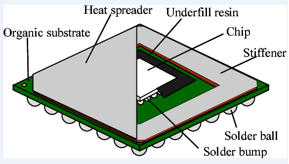
Function and Design: Stiffeners are mounted around the chip edges to prevent substrate warpage and secure the die. They represent the earliest form of packaging-level thermal components, suitable for smaller chips (e.g., Hopper GPUs).
Technology Evolution: As chip sizes grow, new-generation stiffeners are becoming longer and thicker, with materials shifting from stainless steel tocopperfor better thermal conductivity. Advanced stiffeners can even match certain heat spreaders in performance, with ASPs approaching those of thermal lids.
Heat Spreader / Lid

Basic Function: A pure copper lid covers the entire die, supporting and protecting it while conducting heat uniformly to system-level thermal modules (e.g., heat sinks or cold plates). Standard lids typically reduce temperatures by less than 10 °C, so high-power chips often requireheat pipes or vapor chambersfor effective cooling.

Vapor Chamber Lid (VC Lid)


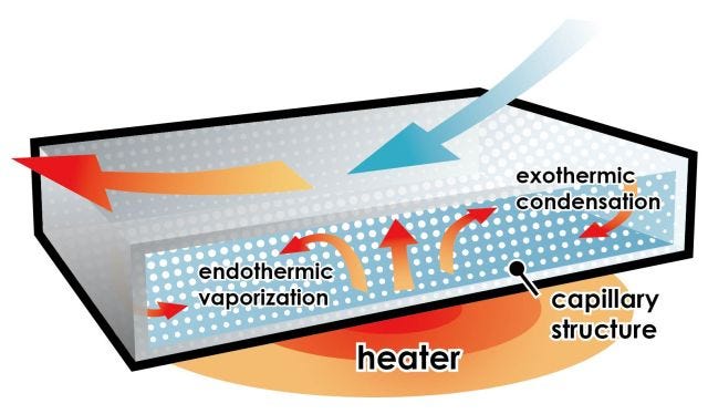
Structure and Principle: VC lids consist of a cavity formed by top and bottom copper plates and copper posts, filled withwater as the working fluid. Heat from the chip causes the liquid toevaporate near the heat source, spreading vapor rapidly throughout the chamber. The vaporcondenses at the cold side(in contact with a heat sink or cold plate) and returns via capillary action, creating atwo-phase, direct-contact cooling loop.
Features and Challenges: The thermal conductivity of vapor is far higher than solid copper, enabling VC lids to outperform pure copper lids. However, they must beco-integrated with the package, arelimited by package footprint, and requirehigh manufacturing precision and long validation cycles(e.g., Jentech spent ~5 years), resulting in few competitors.
In theiPhone 17 ProandiPhone 17 Pro Max, Apple has introduced aVapor Chamber (VC) thermal systemfor the first time, marking a major breakthrough in the company’s approach to thermal management. Unlike previous models that relied primarily on graphite sheets and aluminum frames for heat dissipation, the new VC utilizesa sealed liquid (deionized water)as the working medium. Through continuousevaporation and condensation cycles, it effectively transfers the high thermal load generated by theA19 Pro chip and GPUto the chassis surface, significantly improving performance stability during extended gaming or AI-intensive workloads.
Teardown analyses reveal that Applelaser-welded the vapor chamberdirectly into the aluminum frame, forming anintegrated thermal pathway. This design not only enhances heat spreading efficiency but also maintains structural rigidity and device thinness. Test data indicate that the VC notably reducesthermal throttling, allowing the iPhone 17 Pro to sustain higher performance levels under heavy workloads such as 3D gaming and AI image processing.
However, implementing a vapor chamber in such a compact device also introduces engineering challenges—such as potential chassis deformation from welding stress, long-term sealing reliability of the internal coolant, and maintaining uniform heat distribution. Some users even performed extreme modifications by attaching SSD-style cooling modules to the phone’s back, improving sustained performance stability to over 90%, indirectly demonstrating the VC’s untapped thermal potential.
Overall, the vapor chamber in the iPhone 17 series representsa new milestone in Apple’s mobile thermal design evolution. It not only enables more consistent chip performance but also lays the foundation for future applications inAI computation, augmented reality (AR), and high-resolution imaging—signaling the arrival of anew era of high-power-density, actively managed mobile devices.
Micro-Channel Lid (MCL)

Concept: MCL integrates the functions of a heat spreader and a cold platewithin the package. Micron-scale channels are etched into a copper base and sealed with a lid, withinlet and outlet manifoldsfor coolant flow. The coolant flows directly above the chip, removing heat efficiently and enablinghigher compute density in the same footprint.
Advantages:
Lower thermal resistance & cost benefits— MCL requires onlyone TIM layerbetween the chip and the lid, unlike traditional cold plate solutions which add another TIM layer between the lid and cold plate. This reduces thermal resistance and cost compared to the“lid + cold plate”stack.
Higher content value— According to J.P. Morgan, upgrading an AI server from a traditional lid to an MCL can increase theper-chip thermal solution value by 9–10×.
Timeline and Challenges: MCL adoption is expected tobegin in 2H 2026 and become mainstream by 2027, though supply chain mass production and testing remain bottlenecks. Some forecasts push volume adoption to2027–2028.
More Advanced: Silicon-Integrated Micro-Coolers

Concept: Microchannels areetched directly into the chip or interposer, allowing coolant to flowinside the silicon. Because the coolant contacts the chip directly without any intervening lid or TIM, this approach offersthe lowest thermal resistancepossible.
Current Status and Challenges: This technology is still in thelaboratory stageand may take a decade to reach mass production. Key issues includedie warpage, microchannel design, coolant control, and system integration. Industry expectations are thatMCL will become widespread first, followed by silicon-integrated microfluidic cooling in the longer term.

2025年7月9日
The evolution of thermal management is moving rapidly fromtraditional system-level cooling toward package-level and chip-level integration, driven by the escalating power of AI/HPC processors. Stiffeners, lids, vapor chambers, and MCLs are being commercialized in sequence, withsilicon-integrated micro-cooling representing the next frontier.
System-Level Thermal Technologies in thermal management
Cold Plate
Principle:
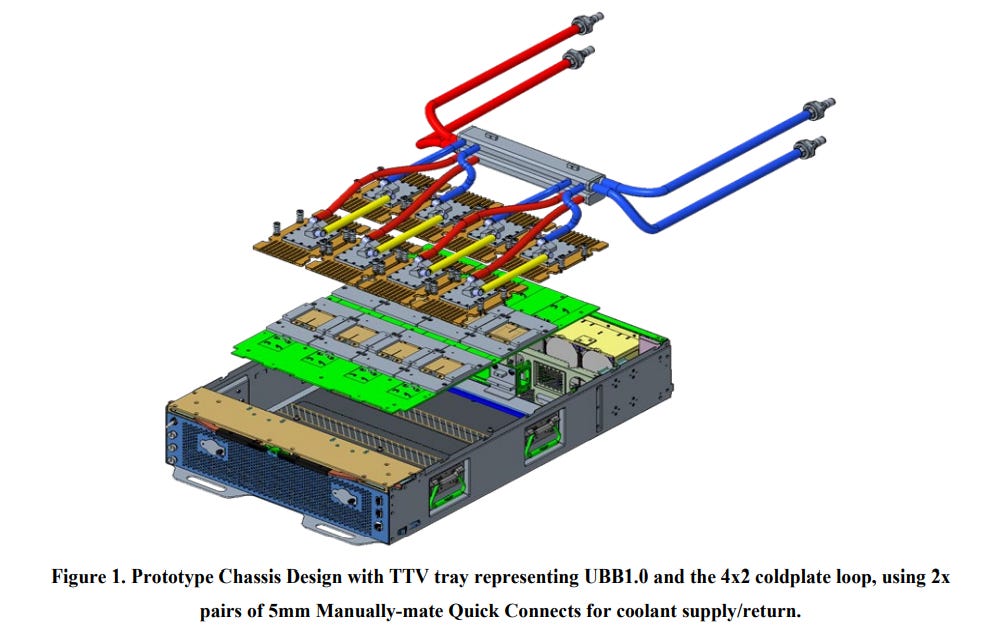
A cold plate is asystem-level liquid cooling modulethat integrates microchannels into a metal plate, with coolant flowing through these channels to absorb heat from the source.Pumped Two-Phase (P2P)cold plates use low-pressure refrigerants to transfer heat throughevaporative latent heat.
The basic process involves pumping liquid refrigerant from a reservoir into the cold plate, where itabsorbs chip heat and partially vaporizes, achieving highly efficient boiling heat transfer. The resulting vapor–liquid mixture returns to a heat exchanger,condenses back into liquid, and is recirculated.
Performance and Advantages:
Due to the extremely high heat transfer coefficient on the cold plate wall during boiling,P2P cold plates can support over 2 kW per chip and 10 kW per system. Chemically inert refrigerants preventcorrosion and biological growthissues common in water cooling systems. In the event of leakage, the refrigerant rapidly vaporizes, minimizing damage to electronics and simplifying maintenance.
Jentech’s Cold Plate Development:

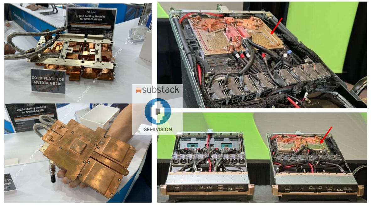
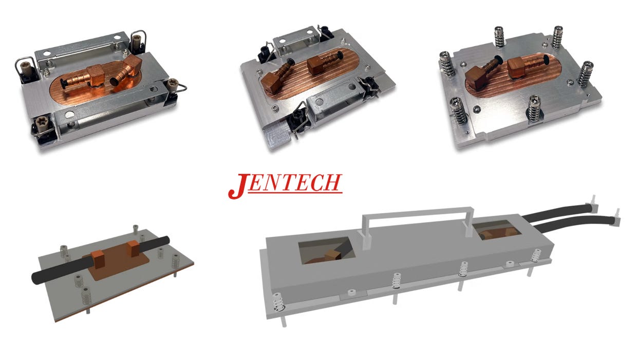
Jentech has extensive liquid cooling experience accumulated from EV power module applications, giving it a unique single-shot forming process that enables high precision and rapid mass production. The company began shipping cold plates for B200 HGX servers in Q1 2025, with more projects scheduled for 2H 2025 and 2026. A single cold plate is priced at roughly 15× that of a heat spreader, contributing significantly to revenue growth.Heat Pipes and Vapor Chambers
Conventional copper lids alone can reduce chip temperatures byless than 10 °C, makingheat pipes and vapor chambersessential for transferring heat to system-level modules. These arevacuum-sealed, two-phase heat transfer devicesthat useliquid–vapor phase changefor efficient thermal transport.
Typically, water is used as the working fluid. When heated, itevaporates, spreads as vapor to the cold end,condenses, and returns via capillary structures—achievingmuch higher effective thermal conductivity.
Heat pipesare linear structures for localized heat transfer.
Vapor chambersare flat, 2D structures that rapidly spread heat across a plane, making them ideal for high heat flux with uniform distribution
Manufacturing Technology and Barriers
Thermal components must be indirect contact with the chip, somanufacturing precision and yieldare critical. Jentech’s competitive edge lies in itsvertically integrated manufacturing capabilities:
Electroplating:Uniform plating on copper and gold is required. Even microscopic voids can cause lid delamination. Jentech developed its own plating equipment and know-how to achieve high yields quickly, creating a significant entry barrier.
Stamping:High-precision stamping must control dimensions, thickness, flatness, and cleanliness. Variability in copper roll quality requires Jentech to fine-tune molds and prevent contamination from iron or copper particles.
Single-shot Forming:In cold plate production, Jentech applies itssingle-shot forming processfrom heat spreader manufacturing, enabling precise, complex structures in a single step with shorter production cycles.
Market Trends and Outlook in Cold Plate
With the rapid increase in AI/GPU and ASIC power, thermal components are evolving from stiffeners → copper lids → vapor chamber lids → micro-channel lids (MCL). The per-chip thermal solution value is expected to grow 9–10× by 2H 2026. Future server designs will integrate multiple chips, further increasing cooling demand.
MCL to Become Mainstream
According to investment reports, chipmakers and packaging/thermal suppliers are accelerating qualification, aiming to adopt MCL in 2H 2026 and reach mainstream adoption by 2027. MCL offers low cost and excellent thermal performance, giving chipmakers strong motivation to adopt. However, actual ramp-up could be delayed by supply chain complexity.
Cold Plate Business Growth
System-level cold plates are used not only in servers but also widely in EV power modules. As data centers shift toward liquid cooling, P2P cold plates will become standard for high-power AI clusters, offering superior heat transfer and lower operational costs. Leveraging EV cooling experience and single-shot forming technology, Jentech holds a leading position in server cold plates.
Long-Term Vision: Silicon-Integrated Cooling
Etching microchannels directly into chips or interposers to let coolant flow within silicon is the ultimate vision. This approach eliminates all interface thermal resistances, pushing cooling performance to physical limits. However, it remains in the lab stage, with commercialization expected to take a decade or more.
The sharp rise in power and heat flux densities in electronic systems has driven thermal technologies from simple copper lids to integrated microchannel and two-phase cooling architectures.
Stiffeners and copper lidsprovide baseline protection and heat spreading.
Vapor chamber lidsenable more efficient packaging-level heat transfer for AI chips.
Micro-channel lidscombine lid and cold plate functions, offering low thermal resistance and cost advantages, and are expected todominate within three years.
At the system level,cold plates and P2P liquid coolingoffer reliable high-power dissipation and play a key role in data center efficiency.
Looking ahead,silicon-integrated microfluidic coolingcould fundamentally reshape chip thermal architectures, though mass production still faces multiple technological hurdles.
2025年7月22日
Core Concept of MLCP (Micro-Channel Liquid Cooling Plate)
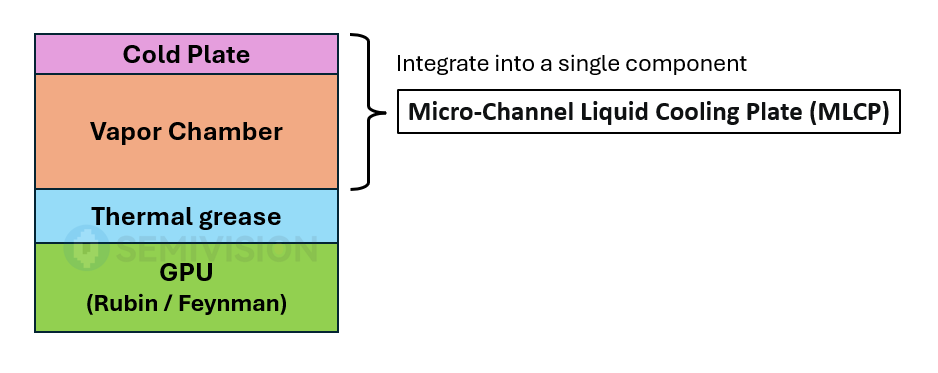
TheMLCPis essentially ahighly integrated direct liquid cooling solution. It consolidates the traditionalIHS (Integrated Heat Spreader),TIM (Thermal Interface Material), andliquid cold plateinto asingle structure, usingmicron-scale microchannelsto allow coolant to directly interact with the chip’s surface heat source.
Key Technical Highlights
Micron-Scale Channels
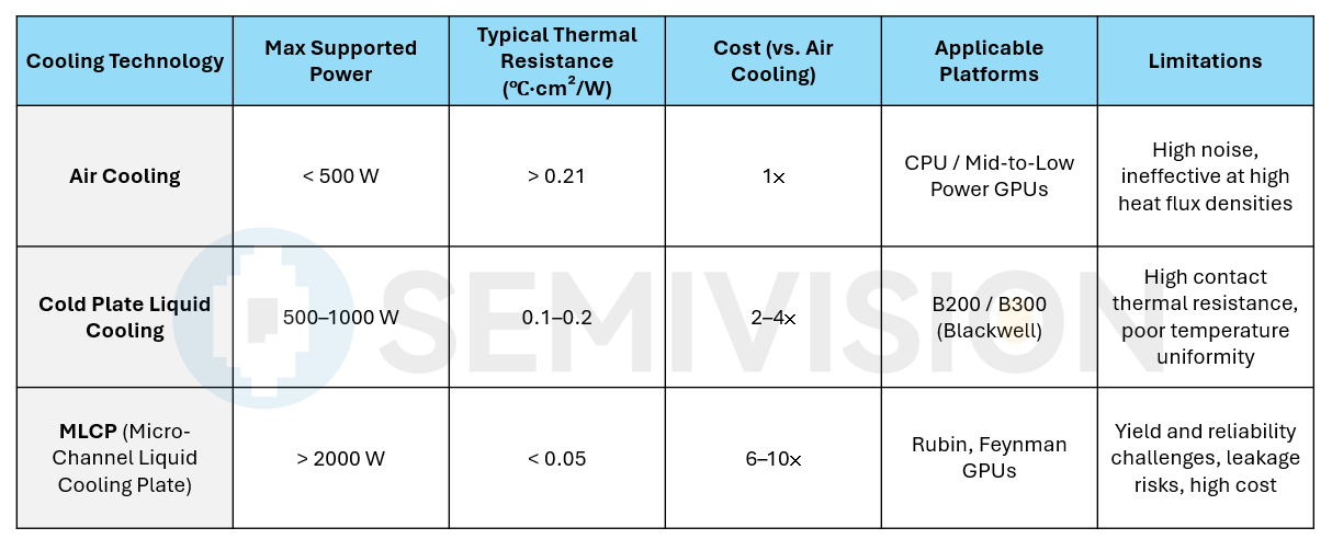
Unlike conventional cold plates that typically usemillimeter-scale channels, MLCP channels areminiaturized to 30–150 μm, dramatically increasing theheat transfer surface area per unit area. This enablesheat flux handling of 600–800 W/cm².
Shortened Thermal Path
Traditional structures include multiple interface layers—TIM, IHS, solder—which stack up thermal resistance. MLCPremoves most intermediate layers, bringing coolant much closer to the chip surface and reducingthermal resistance to below 0.05 °C·cm²/W.
Packaging Integration
The cooling structure shifts from being anexternal attachmentto becomingembedded within the package, co-designed with the GPU/CPU itself. This implies that future thermal solutions will beco-developed alongside IC and package design, rather than added post-design.
Why NVIDIA Needs MLCP
Withgenerative AI driving an explosion in compute demand, theRubinandFeynmangeneration GPUs are expected tofar exceed the cooling limits of current cold plates.

Rubin GPU Power: Dual-die packages are projected to consume2,200–2,300 W per package.
Rack Power: Rubin server racks are designed to support~600 kW total power, nearlydouble the current B200/GB200 rack levels.
Air Cooling Limit: ~500 W per chip is the upper bound for air cooling; beyond40 kW per rack, air cooling becomes completely ineffective.
Traditional Cold Plate Limit: Effective up to500–1,000 W, but struggles toevenly cool multi-chip modules (MCMs)above 2,000 W, often resulting inhot spots.

To ensure stable operation of the Rubin generation, NVIDIA is directly driving suppliers to develop MLCP, reportedly paying 3–5× the price of existing cold plates—underscoring both the necessity and strategic importance of this technology.
Current MLCP Technology Progress and Challenges (AVC & Auras & Cooler Master & JENTECH )
Progress
MLCP is still in the testing and validation stages (EVT/DVT), and it will likely take another 3–4 quarters before it reaches true mass production.
Taiwan’s “big four ” cooling companies —JENTECH,AVC, Auras, and Cooler Master— have already begun sampling to NVIDIA, but production remains limited to prototypes and small batches.
The earliest possible timeline for MLCP mass production is the second half of 2026, starting with the Rubin platform.

Challenges
Leakage risk:If coolant leaks into the package, it can cause server failure worth hundreds of thousands to millions of dollars. Long-term sealing reliability and material aging are the biggest concerns.
Manufacturing yield:MLCP requires microchannel etching on copper or composite materials. These micron-scale structures impose extremely high precision and yield requirements for both fabrication and packaging.
Reliability testing:MLCP must pass JEDEC/IPC reliability standards, including highly accelerated life tests (temperature cycling, pressure cycling, vibration, salt spray), to ensure long-term stability.
Coolant purity:Any metal particles or impurities can clog or corrode the microchannels. This places extremely high demands on datacenter water purity and filtration standards.
Market Potential of MLCP
Using aGB300/Rubin rackas an example:
Each rack requires108 GPUs + 18 CPUs, equivalent to126 MLCP units.
With a unit price of$800–900, thecooling plate cost per rackalready exceeds$100,000.
If NVIDIA ships50,000 racks per year, theMLCP market alonecould exceed$5 billion.

More importantly:
Value uplift of 5–7×:Thermal components will shift from being “low-margin, auxiliary parts” to becoming a core BOM item.
Supply chain reshuffle:Taiwan’s top cooling companies and high-end US/EU suppliers will work closely with OSATs and packaging houses, gaining significantly more influence.
Thermal–packaging co-design:In the future, thermal solutions will be designed alongside BSPDN (Backside Power Delivery) and CPO (Co-Packaged Optics), becoming a foundational element of GPU architecture.
Future Outlook
MLCP is an inevitable choice for the ultra-high-power AI GPU era.
Although still in early validation and facing yield and reliability challenges, the launch ofNVIDIA’s Rubin and Feynman platformsis expected to driveMLCP to become standard between 2026 and 2027.
This marks the start of a new“thermal value revaluation” cycle:
Air cooling and cold plateswill remain, but focus more onmid- and low-power products.
MLCPwill target2,000 W+ GPUsand600 kW racks, becomingindispensable for high-end systems.
For the supply chain,whoever can solve yield and reliability issues first will secure a $5B+ incremental market opportunity.
In-Depth Analysis of Microchannel Cooling Technology
Fundamental Thermal and Fluid Mechanics Principles of Microchannel Cold Plates vs. Conventional Cold Plates
The core concept ofmicrochannel cold platesis to engineermicrometer-scale flow channels, allowing coolant to pass through extremely narrow passages. Compared to conventional cold plates, where channel widths are typically in themillimeter range or larger, microchannel structures usually range fromtens to a few hundred micrometers.
This design leads to two critical effects:
Significantly increased heat transfer area per unit volume or surface area, which dramatically boosts the convective heat transfer coefficient.
Higher local fluid velocityinside the microchannels, which further enhances convective heat transfer.
More specifically, theboundary layer thickness is compressed, and the onset of turbulence occurs under different flow conditions, resulting inheat transfer coefficients an order of magnitude higherthan those of conventional cold plates. Research has shown that microchannel liquid cooling can handleheat fluxes exceeding 1000 W/cm², far outperforming traditional cold plates, which typically manageless than 100 W/cm².
Additionally, microchannel cold plates are mounted inclose proximity to the chip substrate, shortening the thermal conduction path. This leads to amore uniform temperature distribution across the chip surface, effectively minimizing local hot spots. In contrast, conventional cold plates, with their wider channels and longer fluid paths, exhibithigher thermal resistance and less uniform cooling.
In short,microchannel cold plates leverage microscale effects and large surface-area ratios to achieve stronger convective heat transfer and superior thermal performance, whereastraditional cold plates, while simple and cost-effective, struggle to handle the thermal demands of high-heat-flux applications in advanced chips.
Why Microchannels Enable Much Higher Heat Flux Density per Unit Area
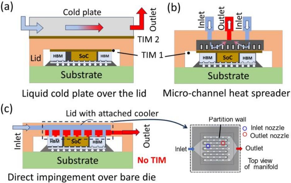
Microchannels can sustain higher heat flux densities primarily due toenhanced heat transfer performance and reduced thermal resistance.
High surface area density:The fine channel geometry provides a much larger heat transfer area compared to macrochannels, dispersing the heat load more effectively.
Increased local flow velocity:As the channel size decreases, local fluid velocity and Reynolds numbers increase (even if the overall flow remains in the laminar regime). Combined withstrong shear effects and turbulence stimulation, this significantly raises theconvective heat transfer coefficient.
As a result, microchannel cooling systems can handleheat fluxes in the kilowatt-per-square-centimeter range. Experimental and industrial implementations have demonstratedlocalized heat flux management of 800–1000 W/cm², while maintaining acceptable junction temperatures.
Overall, the combination ofhigh surface-area density and intensified convectiongives microchannel coolingfar superior heat removal capability per unit areacompared to conventional cooling solutions.
Impact of Microchannel Structures on Two-Phase Flow Distribution and Critical Heat Flux (CHF) in Boiling/Condensation Cooling
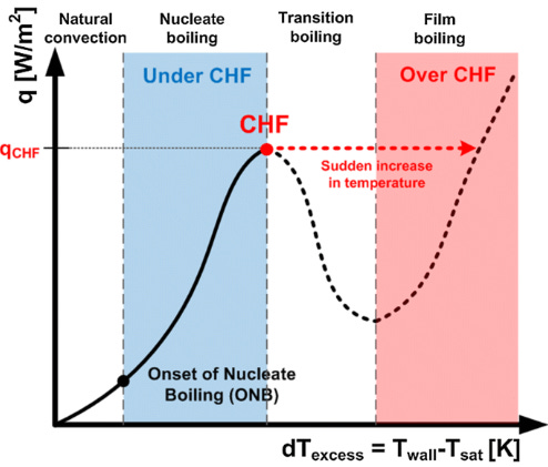
Intwo-phase cooling systems(e.g., flow boiling or flow condensation), thegeometry of microchannel structuresplays adecisive rolein determiningtwo-phase flow distributionand thecritical heat flux (CHF).
Because thecross-sectional dimensions of microchannels are extremely small, vapor bubbles generated during boiling arespatially constrained. Instead of forming spherical bubbles, theyelongate axially into slug-like bubbleswithin the channels, which leads tothinning of the liquid filmand, in some cases,rapid local dryout. According to literature, when channel dimensions are very small,bubble growth is restrictedand theliquid film contact area increases. However, the film can becomevery thin and unstable, and at high heat fluxes,local dryout occurs prematurely, causing asharp deterioration in heat transferand leading toearly CHF onset.
In contrast,increasing the channel cross-section(either in width or height) can improve flow stability by allowinglarger bubbles to form and detach from the wall, enablingliquid replenishmentat the heated surface. Thisdelays dryoutandsignificantly raises the CHF threshold.
Moreover, theshape and connectivityof microchannel structures strongly influencegas–liquid distribution. Researchers have investigated various channel designs, including:
Constant cross-section channels
Gradually expanding cross-section channels
Interconnected adjacent channels(auxiliary flow passages linking neighboring channels)
Experimental results show thatinterconnected channelsprovide themost uniform two-phase distribution, as the auxiliary passages helpbalance flow and pressureamong channels,minimize vapor accumulation, and achievesuperior overall heat transfer performance.
Gradually expanding cross-section channelsallow elongated bubbles in slug flow toexpand and coalesce smoothlyalong the flow direction, promotingbubble transport toward the outlet,reducing downstream blockage, and ensuringtimely liquid replenishment. This structure helpsdelay CHF onsetcompared to uniform channels.
The figure below schematically illustrates these three types of channel geometries:
a) Constant cross-section channels
b) Gradually expanding cross-section channels
c) Interconnected adjacent channels
The Impact of Pressure Drop and Flow Distribution Inside Microchannels on Overall Cooling Performance
Because of the extremely small channel dimensions, fluid flow inside microchannels typically experiences significant pressure drops. This means that the cooling system must rely on more powerful pumps to maintain the required flow rate, thereby increasing system power consumption. However, an appropriate pressure drop can also ensure high coolant velocity, which enhances convective heat transfer efficiency. Therefore, microchannel design must carefully balance heat transfer gains against pumping power losses.

Advanced solutions—such asMikros Technologies’ Normal Flowapproach—optimize channel flow paths to significantly reduce the inherent high pressure drop of microchannels while maintaining excellent thermal performance. For example, measurements show that a 2 × 2 cm microchannel cold plate experienced a pressure drop of less than 1 psi (~6.9 kPa) at a flow rate of 1 L/min, allowing it to handle kilowatt-level heat loads without requiring excessive pumping power. Another example involves the implementation of cross-flow manifold designs, which reportedly reduced the pressure drop by 88% at 350 mL/min flow rate, while also achieving more uniform chip temperature distribution.

Flow distribution uniformity is equally critical. In parallel multi-channel microchannel cold plates, central channels typically receive higher flow rates while edge channels experience lower flow rates, leading to uneven cooling and localized hotspots. To address this, auxiliary interconnecting channels can be introduced between parallel channels to equalize fluid distribution. Studies show that such interconnect structures balance pressure and flow among channels, effectively mitigating early boiling in the center channels and preventing premature dryout at the edges. This results in more stable overall heat transfer and delays the onset of CHF.
In summary, pressure drop and flow distribution within microchannel heat sinks directly affect pumping power, fluid temperature rise, and chip temperature uniformity. An effective design must ensure sufficient flow velocity for efficient heat transfer while minimizing unnecessary hydraulic losses and optimizing flow distribution, ultimately maximizing the overall cooling performance.
Heat Flux Density Supported by Microchannel Cooling in AI/HPC Chip Applications
As the power density of AI/HPC chips continues to rise sharply, the ability of microchannel cooling to handle extremely high heat flux densities has attracted significant attention. Reported results show that microchannel technology can support heat flux levels far beyond traditional cooling solutions.
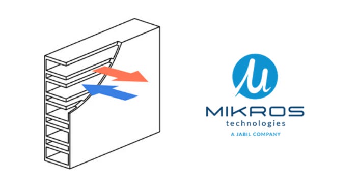
Mikros Technologies claims that its microchannel cold plates can support heat fluxes up to 1000 W/cm², with an exceptionally low surface thermal resistance of approximately 0.02 °C/(W/cm²). Another study indicates that under single-phase water cooling, both simulations and experiments have demonstrated that microchannels can easily dissipate 800 W/cm² or more, while maintaining the chip junction temperature within a controlled range. More broadly, literature reports show that microchannel liquid cooling systems can handle heat flux densities ranging from 100 to 2000 W/cm².
These findings clearly indicate that microchannel cooling far exceeds the few hundred W/cm² levels currently required by GPU and ASIC devices, and can meet the thermal demands of future high-power AI chips. Of course, achieving reliable operation under extreme heat fluxes requires further optimization—such as integrating phase-change cooling and enhanced two-phase flow designs—but both current research and industrial applications have already demonstrated that microchannel cooling can provide robust, high-capacity thermal management in the hundreds to thousands of W/cm² range for next-generation high-performance chips.
Common Microchannel Fabrication Techniques: Advantages and Disadvantages
Microchannel cold plates can be fabricated using various manufacturing methods. The most common techniques includesilicon micromachining,laser processing,micro-milling/electrical discharge machining (EDM),micro-casting or metal injection molding (MIM), and theemerging 3D printing (additive manufacturing)technologies.
Etching (Silicon Micromachining):
This method uses photolithography and deep reactive ion etching (DRIE) to carve micrometer-scale channels on silicon wafers, followed by bonding with another silicon or glass wafer. It is well-suited for MEMS-level precision, enablinghigh aspect ratio channelswithsmooth channel walls. However, the process iscomplex, involving multiple photolithography, doping, and bonding steps, andcosts are high.
Laser Processing:
By focusing a laser beam, microchannels are ablated directly on the surface or within the bulk of materials. Laser processing ishighly versatile, applicable to silicon, glass, metals, and even ceramics. It requiresno photolithographic molds, isflexible, and offersfast processingspeeds. Research shows thatlaser micromachining has become an effective methodfor fabricating microchannels, thanks to itsspeed and cleanliness(avoiding chemical residues from etching). However,surface roughness tends to be higher, requiring post-processing (e.g., cleaning or polishing), and thefocal depth is limited, making it difficult to create very deep channels in a single pass.
Mechanical Machining (Micro-milling / EDM):
Using micro-cutters or electrodes, channels are directly machined intometal substrates(e.g., copper, titanium alloys). This is amature and direct methodfor metals, suitable forchannel sizes above tens of micrometersand forlarge workpiece areas. However, machiningprecision is limited by tool size, surfaces often exhibit machining marks,tool wear is rapid, andprocessing time is longer.
Micro-casting / Injection Molding:
A mold with anegative microchannel pattern(produced via silicon etching or electroforming) is used to replicate microchannel structures throughmetal injection molding,die casting, orplastic injection molding. This technique iswell-suited for mass production, offeringhigh replication efficiency, butmold fabrication is expensive and time-consuming, making it viable only for high-volume production.
3D Printing (Additive Manufacturing):
Techniques likeSelective Laser Melting (SLM)enable the one-step fabrication ofcomplex 3D microchannel geometrieswithout bonding. However,current resolution limitsmean theminimum channel size is typically in the hundreds of micrometers, andsurface roughness is relatively high, requiring careful parameter optimization.
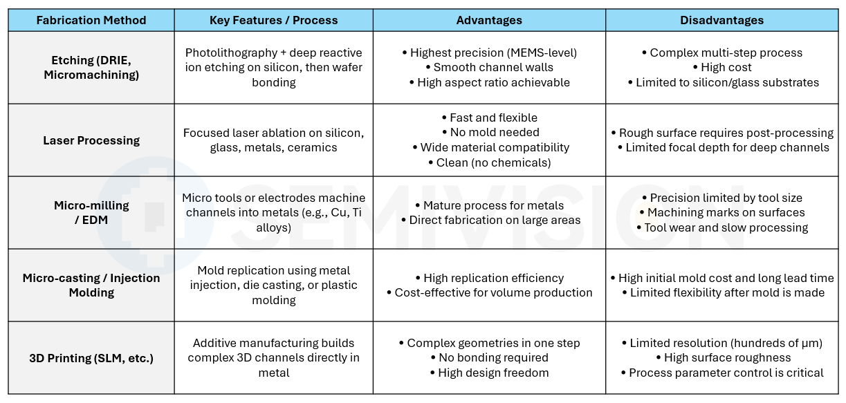
Etchingis best for precision and smoothness but expensive and limited to silicon.
Laseris the most flexible and fastest but needs post-polish for thermal performance.
Mechanical machiningis robust for metals but limited in miniaturization.
Moldingdominates in high-volume, stable designs.
3D printingis promising forcomplex, integrated cooling designs(e.g., AI server MLCP), but resolution and surface finish remain technical bottlenecks.
Machining Challenges for Different Materials (Silicon, Copper, SiC, Ceramics)
Microchannel cold plates are typically made from materials withhigh thermal conductivity and good mechanical strength, but each material presents distinctfabrication challenges:
Silicon:
Silicon wafers can be processed usingmature semiconductor techniques(photolithography + etching) to fabricatehigh-precision microchannelswith smooth walls and dimensional control down to tens of nanometers. However, silicon has amoderate thermal conductivity(~150 W/m·K), which is lower than copper. Fabrication requirescleanroom environments, making costs relatively high. In addition, silicon isbrittle, making it unsuitable for high-pressure applications without reinforcement.
Metals (Copper, Titanium):
Copper offersvery high thermal conductivity(~400 W/m·K), making it ideal for heat dissipation. However,machining copper is challenging: it is prone tomicrocracks,surface oxidation, andrapid tool wear, whilemicro-milling is slow and inefficient. In two-phase flow environments, copper issusceptible to corrosion, requiringsurface passivation or protective coatings. Titanium alloys providebetter strength and corrosion resistance, but theirthermal conductivity is lowerthan copper.
Silicon Carbide (SiC):
SiC combinesexceptional thermal conductivity(up to ~490 W/m·K),excellent thermal shock resistance, and alow coefficient of thermal expansion, making it highly suitable forhigh-temperature and near-chip cooling applications. However,SiC is extremely hard, making traditional mechanical machining unsuitable for fine features. Instead,laser ablation,ultrasonic grinding, or otherhigh-cost techniquesare required. Additionally,SiC is expensive, and its processing steps are complex.
At the 2025 IEEE conference, a paper titled“Integrated Thermal Management for a High-Power-Density Silicon Carbide Power Module With Die-Level Heat Flux Over 1000 W/cm²”was published, focusing on achieving highly efficient thermal management for high-power-density SiC power modules. The research team combinednano-silver sintering (nano-Ag sintering)withmanifold microchannels (MMCs)to propose an integrated package-level cooling architecture capable of maintaining ajunction temperature below 127 °C under a die-level heat flux of 1000 W/cm². ThroughCFD simulations and experimental validation, the authors compared traditionalpin-fin heat sinkswith two innovative MMC designs—tapered Z-type (TZMMC)andconnected Z-type (CZMMC). The results showed that theCZMMCachieved thelowest thermal resistance of 9.85 mm²·K/W (≈ 0.066 K/W), representing an80% reduction in thermal resistanceand an83% decrease in pumping powercompared to conventional liquid-cooled modules. Moreover, the integrated design improvedtemperature uniformity and reliability, resulting in a138% increase in current densityanddoubling the output current capabilityof the power module. This study demonstrates that MMC-integrated cooling can simultaneously achievehigh thermal efficiency, low pressure drop, and packaging compatibility, providing a key technological pathway for next-generationSiC power modulesin automotive, grid, and high-voltage applications requiring ultra-high heat flux dissipation.

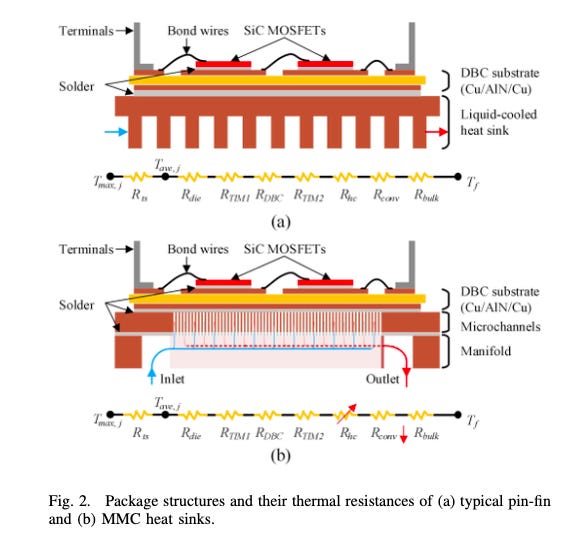

In another study titled“A Highly Efficient Manifold Microchannel Heat Sink for Extreme Heat Flux Dissipation in High-Power SiC Devices,”the researchers addressed the thermal management challenges of high-power-density SiC chips and proposed a high-performanceManifold Microchannel Heat Sink (MMC-HS)design. By combining athree-dimensional fluid distribution structurewithlow thermal resistance packaging materials, the team validated through CFD simulations and experimental testing that the system can maintain thechip junction temperature below 120 °C under a heat flux exceeding 1000 W/cm². The newly designed“distributed inlet with localized recirculation”microfluidic topology significantly reduces pressure drop and enhances cooling uniformity. Compared with conventional pin-fin and single-channel liquid cooling schemes, the MMC-HS achieves a70–80% reduction in total thermal resistanceand anapproximately 85% reduction in pumping power. Furthermore, the design demonstrates excellentpackage-level integration, as it can be combined withnano-silver sintering interfacesto form a module-level thermal solution with high thermal conductivity, low mechanical stress, and superior reliability. This study confirms that MMC-based cooling technology is akey integrative approachfor managing extreme heat flux in futureSiC power modules, AI accelerators, and high-voltage power systems.
In the proposedSiC-on-MMC (Silicon Carbide on Manifold Microchannel)architecture, thefluidic channel designserves as the core of the entire thermal management system. Instead of etching microchannels directly into the SiC die or substrate, thehigh-thermal-conductivity SiC power chipisbonded via nano-silver sinteringonto ametallic or silicon-based manifold microchannel layer (MMC). This configuration efficiently transfers the intense heat generated by the SiC die (exceeding 1000 W/cm²) directly into the coolant within the microchannels, forming anultra-short heat transfer path.
Within the MMC layer, athree-dimensional manifold networkdistributes coolant uniformly from multiple inlets to the microchannels, while localized recirculation regions minimize pressure loss and dead zones. This“manifold–collector” topologyimproves flow uniformity and enhances local convective heat transfer, achieving a chip surface temperature gradient (ΔT) of less than5 °C. Compared to conventional single-pass cold plates, theSiC-on-MMC structurereduces thermal resistance by70–80%and decreases pumping power by more than80%, while maintaining structural integrity and mechanical stability.
More importantly, thislayered integration strategypreserves thehigh thermal conductivity and electrical isolationcharacteristics of SiC, avoiding the fragility and reliability issues that would arise from machining microchannels directly inside the SiC substrate. Overall, theSiC-on-MMC fluidic channel designrepresents a next-generation liquid-cooling architecture that combineshigh heat dissipation capability, mechanical reliability, and packaging compatibility, making it highly suitable forautomotive inverters, high-voltage DC converters, and AI power modulesoperating under extreme heat flux conditions.

Ceramics (e.g., Al₂O₃, AlN):
Ceramics such as aluminum nitride (AlN) offer high thermal conductivity (>200 W/m·K) and excellent electrical insulation, making them popular for power electronics substrates. However, ceramics are difficult to machine and are typically processed using laser machining or reaction sintering to form channels. Their brittleness also means that stress management during packaging is critical to avoid cracking.

Methods to Ensure Geometric Accuracy and Surface Roughness of Microchannels During Fabrication
The geometric precision and wall smoothness of microchannels have a significant impact on pressure drop and heat transfer stability during operation. In practice, a combination of precision micro/nano-fabrication and post-processing techniques is typically employed.
For silicon microchannels, Deep Reactive Ion Etching (DRIE) with cyclic etching–passivation (Bosch process) is commonly used to minimize etching burrs. After the channels are formed, oxidation annealing and chemical mechanical polishing (CMP) are applied to smooth the channel walls.
For laser-processed materials, additional secondary polishing or chemical cleaning steps are often introduced to remove splatter and surface irregularities.
As noted in industry practices,“the machining accuracy requirements for microchannels are extremely high, which also poses challenges for sealing performance.”To maintain millimeter- or even micrometer-level geometric tolerances, high-resolution photolithography masks or precise tool alignment techniques are required. In the design stage, it is also important to consider appropriate channel aspect ratios and avoid excessively thin walls to reduce machining errors.
In actual production, in-line inspection methods such as microscopy and profilometry are used to provide real-time feedback and adjust process parameters. Excessive inner wall roughness can lead to local flow turbulence and increased pressure drop; therefore, post-processing steps such as chemical etching (“etch-polishing”) or electroplating are often applied to further improve surface finish.
By using high-precision molds, optimized etching/engraving parameters, and post-polishing treatments, it is possible to effectively control both the geometric tolerances and surface quality of microchannels, thereby preventing excessive pressure loss or flow instabilities caused by irregular surfaces or dimensional deviations.。
Addressing Interface Material and Reliability Issues in Direct-to-Chip Bonding of Microchannels
When microchannel cooling structures are directly bonded to chips (or multi-chip modules), two critical challenges must be addressed: the selection of thermal interface materials (TIM) and long-term reliability. Because the contact surfaces between the microchannel structure and the chip top surface often have micron-level height variations or warpage, it is essential to use high thermal conductivity and thin interface materials.
In practice, high-conductivity phase-change materials (PCT) or nano-filled thermal greases are commonly used to fill these micro-gaps. For example, in Mikros’ case, a 4.5 W/m·K high-conductivity phase-change paste with a thickness of only 40 μm was used, achieving an internal interfacial thermal resistance as low as 0.10 °C/(W/cm²).
Alternatively, metal solders (e.g., AuSn eutectic, InSn alloys) or silver glass adhesives can be used for rigid bonding, which provides more stable contact pressure and lower thermal resistance. However, rigid soldering introduces additional thermal stress, making it essential to carefully match the coefficient of thermal expansion (CTE) of the materials to avoid microcracks during long-term thermal cycling.
More recently, direct silicon-to-silicon bonding (e.g., silicon–silicon oxide bonding) has been proposed, enabling high-conductivity solid-state joints without any intermediate materials — though the process requires extremely tight control. Regardless of the bonding method, reliability testing is essential, including thermal cycling and pressure leak tests, to ensure the interface remains intact without delamination, leakage, or cracking under high temperature and pressure conditions.
By using ultra-thin, high-conductivity TIMs or high-strength solder joints, combined with CTE-matched materials (such as bonding silicon microchannel cold plates directly to silicon chips), and performing rigorous reliability qualification, the interface challenges in direct-to-chip microchannel integration can be effectively addressed.

Uniform Cooling and Large-Scale Integration for Large AI Chips
For large AI chips, microchannel cold plates must cover wide areas while ensuring uniform heat removal. This is typically achieved by distributing the microchannel array into zones and designing appropriate inlet/outlet manifolds or flow distribution networks to equalize flow velocity across different regions.
For example, primary and secondary flow channels can be arranged for central and edge regions, or cross-compensation channels can be added within the channel grid to balance local flow. As previous studies have noted, interconnecting adjacent parallel channels can effectively eliminate temperature non-uniformities between central and peripheral regions by balancing the flow distribution.
For ultra-large-scale integration, a distributed multi-module microchannel cold plate architecture can be adopted: the chip area is divided into multiple cooling units, each with independent fluid supply, and integrated into a higher-level unified manifold system.
At the package level, microchannel structures can be pre-etched into the substrate and later sealed with a lid to form the cold plate, achieving co-packaged integration directly at the packaging stage.
In short, by optimizing manifold design, zonal cooling strategies, and hierarchical integration, it is possible to achieve uniform cooling and scalable packaging integration for large-area AI chips.
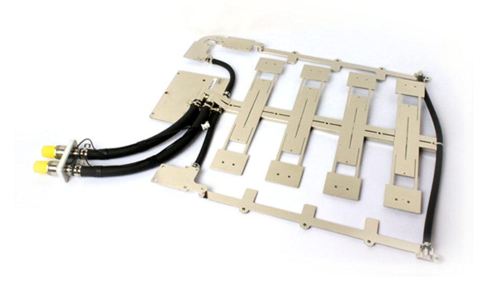
Mikros’ Normal Flow™ microchannels can be fabricated in a wide array of complex topologies. Our cold plates range from 4x4mm to 300x500mm assemblies with many cooling areas. We design custom features to accommodate component height and tilt tolerances, CTE-matching, TIM force requirements and non-planar cooling areas.
Will Microchannel Cooling Replace Traditional Cold Plates and Vapor Chambers as the Mainstream AI Chip Thermal Solution?
As AI chips continue to push the limits of power density, microchannel cooling technology is increasingly emerging as the mainstream solution for high-power-density device cooling, thanks to its exceptionally high heat dissipation capability and compact structure.
Industry studies and technical reports have pointed out that“microchannel cooling is gradually becoming the mainstream thermal management solution for high power density electronic devices.”Compared with traditional air cooling or standard cold plates, microchannel liquid cooling offers dramatically higher heat dissipation capacity and can be custom-designed for hotspot management. These advantages are driving adoption across high-performance computing (HPC) servers, data centers, and other high-power systems.
In fact, multiple leading companies have already introduced microchannel cold plates in their next-generation GPUs and AI accelerators, supporting heat flux densities from several hundred to over a thousand W/cm².
While traditional cold plates remain cost-effective and simple for low-power applications, they are inadequate for future cooling demands at tens to hundreds of W/mm². Under these conditions, microchannel cooling is virtually the only viable solution.
Therefore, it is foreseeable that microchannel cooling will replace conventional cold plates and vapor chambers, becoming the mainstream thermal management strategy for AI chips in the coming years.
Can Microchannels Be Directly Integrated into the Packaging Level in the Context of 3D Stacking and Heterogeneous Integration (HBM + GPU/ASIC)?
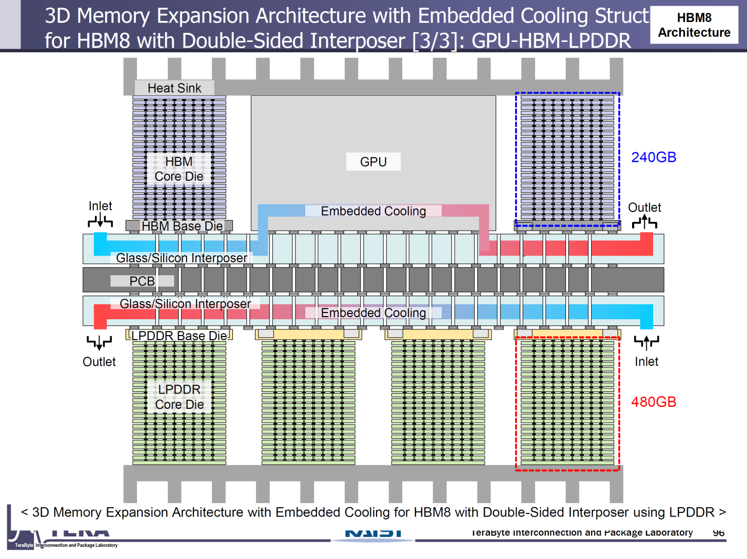
In a recent presentation by KAIST (Korea Advanced Institute of Science & Technology (KAIST), with the rise of 3D stacking and heterogeneous integration, chip packaging has become more complex, placing higher demands on thermal management. Recent research has exploredembedding microchannel structures directly into the packaging levelto enhance cooling performance.
For example, some research teams have fabricatedmicrochannels inside silicon substrates or interconnect layers(e.g., TSV layers) in advanced 2.5D/3D ICs to enableinter-layer flow boiling cooling. Reports have also documentedmicrochannels etched into silicon–GaN substrates, followed byflow boiling experiments, demonstrating the energy efficiency potential of“on-chip microchannel cooling.”
Similarly,fluid channels can be designed within interposer layers(e.g., silicon interposers) between HBM and GPUs to enablecross-chip heat removal.
Overall, while integrating microchannels at the packaging level requires addressing challenges such aspackage reliabilityandinterconnect density, thetechnical feasibility has been demonstrated through early prototypes. Therefore, under 3D stacking architectures, integrating microchannels into the packaging layer (chip-level or interconnect-level channels) is emerging as a promising thermal solution.
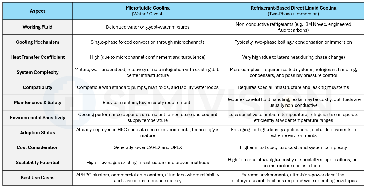
Microfluidic Cooling vs. Refrigerant-Based Direct Liquid Cooling — Which Is More Likely to Scale Commercially?
Microfluidic cooling(e.g., water or glycol-based circulation through microchannels) andrefrigerant-based direct liquid cooling(often two-phase refrigerant loops or immersion cooling) each have unique advantages.
At present,water-based microfluidic coolingis widely deployed inhigh-performance computing (HPC)due to itsmature system architecture,high efficiency, and compatibility with existingdata center cooling infrastructure.
In contrast,refrigerant-based cooling, includingimmersion cooling, offershigh heat transfer coefficientsandlower sensitivity to ambient temperature, making it suitable for specific applications. However, it typically requiresspecial non-conductive fluidsand involves morecomplex system design.
It is too early to definitively say which technology will dominate. Likely scenarios include:
Refrigerant-based two-phase coolingwill be adopted inextreme environments, ultra-high power applications, or scenarios with strict cleanliness requirements (e.g., military or research facilities).
Water-based microchannel coolingwill remain more prevalent incommercial data centers and AI accelerator clustersdue to cost and maintenance advantages.
In short,both approaches have large-scale commercialization potential, with the choice depending onapplication requirements,cost considerations, andsafety factors. (Note: No conclusive literature currently states which will ultimately prevail.)
Will Microchannels Be Combined with Silicon Photonics (SiPh) or Co-Packaged Optics (CPO/OIO) to Provide an Integrated Thermal–Optical Platform?

Silicon photonics and co-packaged optics are becoming increasingly integrated with electronic devices, and they havesignificant thermal management requirementsof their own. Research has begun exploringmulti-functional substratesthat integrate boththermal managementandoptical interconnect components.
For example, it is conceivable toetch microchannels in silicon interposers that host silicon photonic waveguides, placingfluidic cooling channels adjacent to optical waveguidesto achievesimultaneous thermal management and optical signal routing.
In fact, some studies have designedcooling plates for CPO modulesto manage optical module thermal loads, but these are typically implemented at amacro cold plate level, not within the substrate.
To realizetrue on-substrate thermal–optical integration,process compatibilitychallenges must be solved — e.g., co-integratingwaveguide fabricationandmicrochannel etchingwithin the same silicon process flow.
While still at the exploratory stage, the technological trend suggests thatmicrochannel cooling and optical interconnects may co-evolve at the packaging level, leading tohybrid electro-optical substratesthat provide bothhigh-bandwidth photonic interconnectsandefficient heat removal.

2025年6月27日
Innovations Required for Microchannels to Handle 5000 W+ AI Chips (e.g., PCM Integration, Two-Phase Flow Control, Smart Monitoring)
Assingle-chip or module power exceeds several kilowatts, current microchannel technologies will need to incorporateadditional innovationsto maintain stable thermal performance.
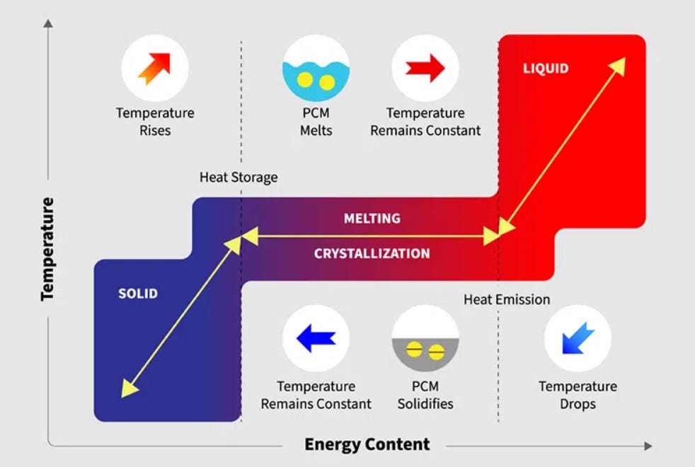
Phase Change Materials (PCMs)can absorb short-term power spikes and release heat gradually. For example,microencapsulated PCMsorphase-change fluidscan be embedded near hotspots tosmooth thermal transientsandlimit junction temperature peaks.
Two-phase flow controlwill also become increasingly critical. This includesprecise management of bubble generation, fluid return, and flow distribution, potentially usingelectromagnetic fieldsormicroelectrodesto actively control boiling dynamics.
Intelligent sensing and monitoringcan be achieved by embeddingmicro flow and temperature sensor arrayswithin cold plates to monitor local conditions in real time. Amicrocontrollercan then dynamically adjustpump speedsorflow distribution, enablingadaptive thermal management.
Forextreme heat flux scenarios, research has begun combiningnovel high-thermal-conductivity materials(e.g.,Cu–diamond composites) withopen microchannel structures, allowing stable operation even at>1000 W/cm²heat flux.
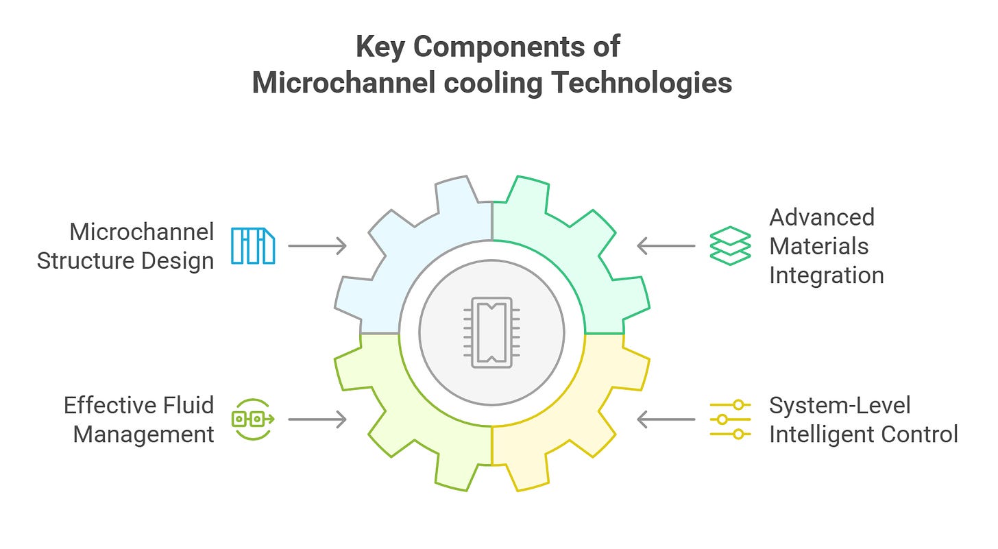
In short, to address the5000 W+ era, innovation is needed across:
Microchannel structure design
Advanced materials integration
Fluid management strategies
System-level intelligent control
Studies have shown that combiningnext-generation thermal materialswithoptimized microchannel geometriescan dramatically enhance cooling stability under extreme conditions.
Microchannel cooling technologydramatically enhances heat transfer efficiency and heat flux handling throughmicron-scale flow channels. Although manufacturing challenges vary by material and integration strategy, microchannels are poised to become deeply intertwined withadvanced packaging technologies, including3D stackingandco-packaged silicon photonics.
By leveragingnew materials,innovative architectures, andintelligent control, microchannel cooling is expected to providehighly efficient, reliable, and scalablethermal management solutions for next-generation AI chips.
This analysis is based on recent literature and industry reports, aiming to provide insights for both research and engineering practices in microchannel cooling.

Technological Breakthroughs and Industrialization Challenges of Microchannel Liquid Cold Plates (MLCP) in the AI Era
Demand Driven by NVIDIA: From Rubin to Rubin Ultra
As AI chip power continues to surge, NVIDIA’sRubin and Rubin Ultra GPU platformshave surpassed the2,000 W thermal barrier, a level that conventional air cooling and standard cold plate solutions can no longer handle. FollowingJensen Huang’s directive to the supply chain,microchannel liquid cold plates (MLCP)have emerged as theonly viable advanced cooling solutioncapable of supporting 2000 W+ GPUs.
Unlike traditionalindirect cooling, MLCP brings the coolantdirectly into micron-scale channelsabove the chip surface, reducing thermal resistance from>0.3 ℃·cm²/Wdown to0.03 ℃·cm²/W—with some experimental data approaching0.01 K/W. This dramatic thermal performance has made MLCP astrategic priority for NVIDIA’s ecosystem, ensuring next-generation GPUs can maintain competitivefrequency and energy efficiencyunder extreme power densities.
Performance Leap: From Classical Models to Breakthrough Structures
MLCP represents a leap frommacroscopic Fourier-based heat transfertomicroscale physical phenomenain thermal design.
Peking University (Song Bai’s group)proposed amanifold–microjet–serrated microchannelstructure that can handleheat fluxes up to 3,000 W/cm², achieving a thermal resistance of0.036 K·cm²/Wat a flow rate of120 mL/min—far surpassing current industry norms.
Xidian University (Duan Baoyan’s team)developed awing-shaped cavity fin disturbance + secondary channel design, reducing peak temperature by21% under 240 Wthermal load and maintainingtemperature uniformity within 4 K.
These results highlight MLCP’s potential to sustainstable, ultra-efficient heat removaleven under extreme conditions, positioning the technology as acore enabler for AI/HPC chips.
Market Scale and Penetration: Liquid Cooling Becoming Mainstream
Liquid cooling is rapidly shifting fromlaboratory technology to commercial realityin server and AI rack deployments.
Morgan Stanleyprojects that China’s liquid cooling penetration rate will rise from12% in 2023to35% by 2025.
Goldman Sachsforecasts theglobal liquid-cooled server marketwill reachUSD 12 billion by 2025, with aCAGR of 45%.
Today,cold plate solutionsaccount for>60%of the market, whileimmersion coolingholds around20%.Microchannel cooling, though still emerging, isgrowing the fastestand is expected tobecome mainstream within three years. This indicates that thecommercialization window for MLCP is opening rapidly, and market acceptance is no longer a key barrier.
Supply Chain Landscape: From Thermal Vendors to System Integrators
Multiple companies areracing to establish their positionsacross the MLCP value chain:
Inspur/Invek(China) has launched itsCoolinsideliquid cooling solution, with200 kW per rack capacityand secured1,200 units of NVIDIA GB300 cabinets, representingnearly 50% of the China market.
Jentech (Taiwan)has become acore MLCP design partnerand is undergoing NVIDIA platform qualification.
Frore, Auras, and Sunonare leveraging theirexisting heat spreader and fan supply chainsto enter MLCP design and manufacturing.
Dunan EnvironmentandNingbo Jingda(China) are extendingmicrochannel technology to EVs and energy storage systems, serving clients such asBYD,NIO, andCATL.
These developments indicate that MLCP is evolving beyond AI GPUs intobroader energy and electronics applications.
Manufacturing Breakthroughs: Metal 3D Printing and Precision Sealing
One of MLCP’s key challenges isfabricating metal microchannelswithmicron-level precisionwhile ensuringreliability and scalability.
Metal 3D printinghas emerged as a key solution. Companies likeCoolestDCandEOShave demonstratedweld-free copper cold platescapable of withstanding6 bar water pressure, effectively reducing leakage risks.
Green laser machininghas overcome the challenge ofhigh copper reflectivity, enabling33 μm-resolution fin structures.
These process innovations not only improve MLCP’s technical feasibility but alsolay the foundation for mass production.
Investment Opportunities and Key Components: From UQD to 3D Printing
MLCP adoption drives demand fornew components and equipment.
NVIDIA’sGB200 platformrequires126 pairs of UQD quick connectors(USD 45 each), whileGB300 increases this to 252 pairs(USD 75–80 each), significantlyexpanding market size.
If MLCP becomes thestandard thermal solution,hundreds to thousands of metal 3D printerswill be required for volume manufacturing.
From Technical Savior to Industry Standard
MLCP has reached apivotal transitionfromlaboratory innovation to industrial deployment. Driven byNVIDIA,microchannel liquid cold plates are rapidly becoming the thermal backboneof the AI/HPC era.
Academic breakthroughs (Peking University, Xidian University) andindustrial execution(Invek, Jentech) show that the technology hasmoved beyond theory.
In the future, MLCP will not only support2,000 W–5,000 W AI chips, but alsoexpand into EVs, power electronics, and aerospace. Withmaturing supply chainsandincreasing investment,microchannel liquid cooling is expected to become the mainstream thermal solution by 2027, defining theinfrastructure of the next compute era.
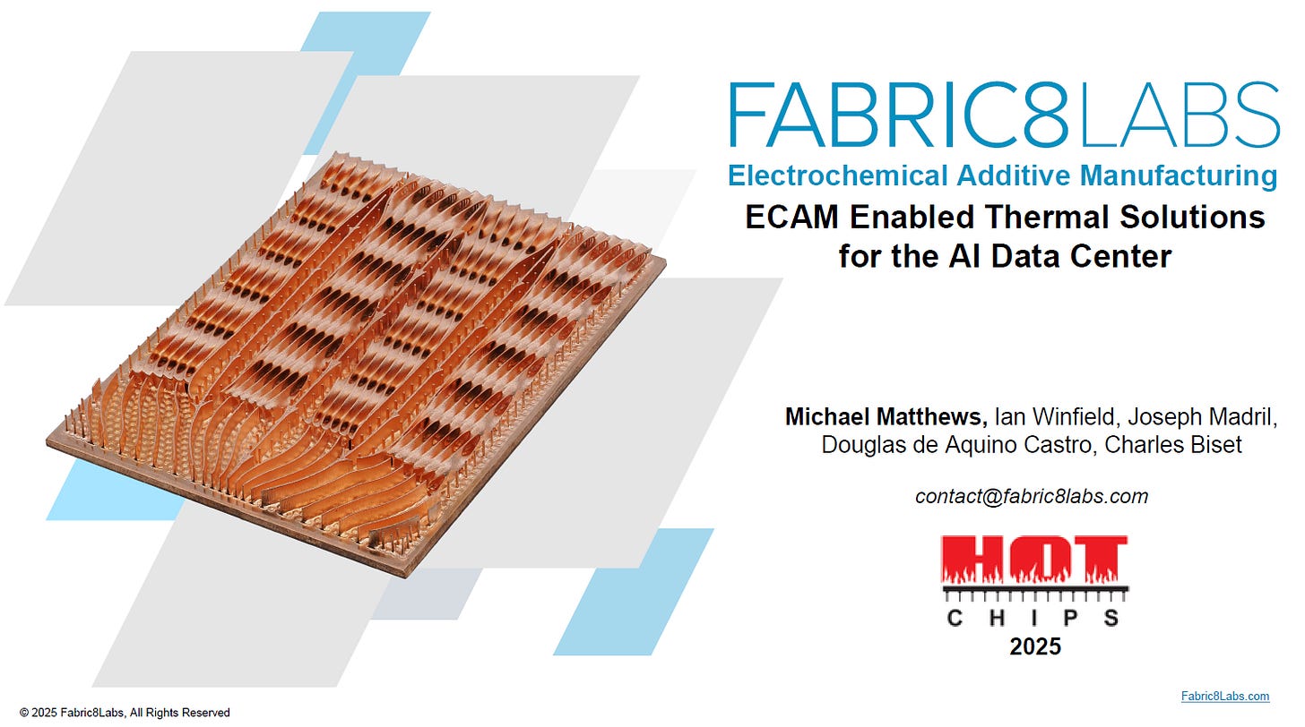
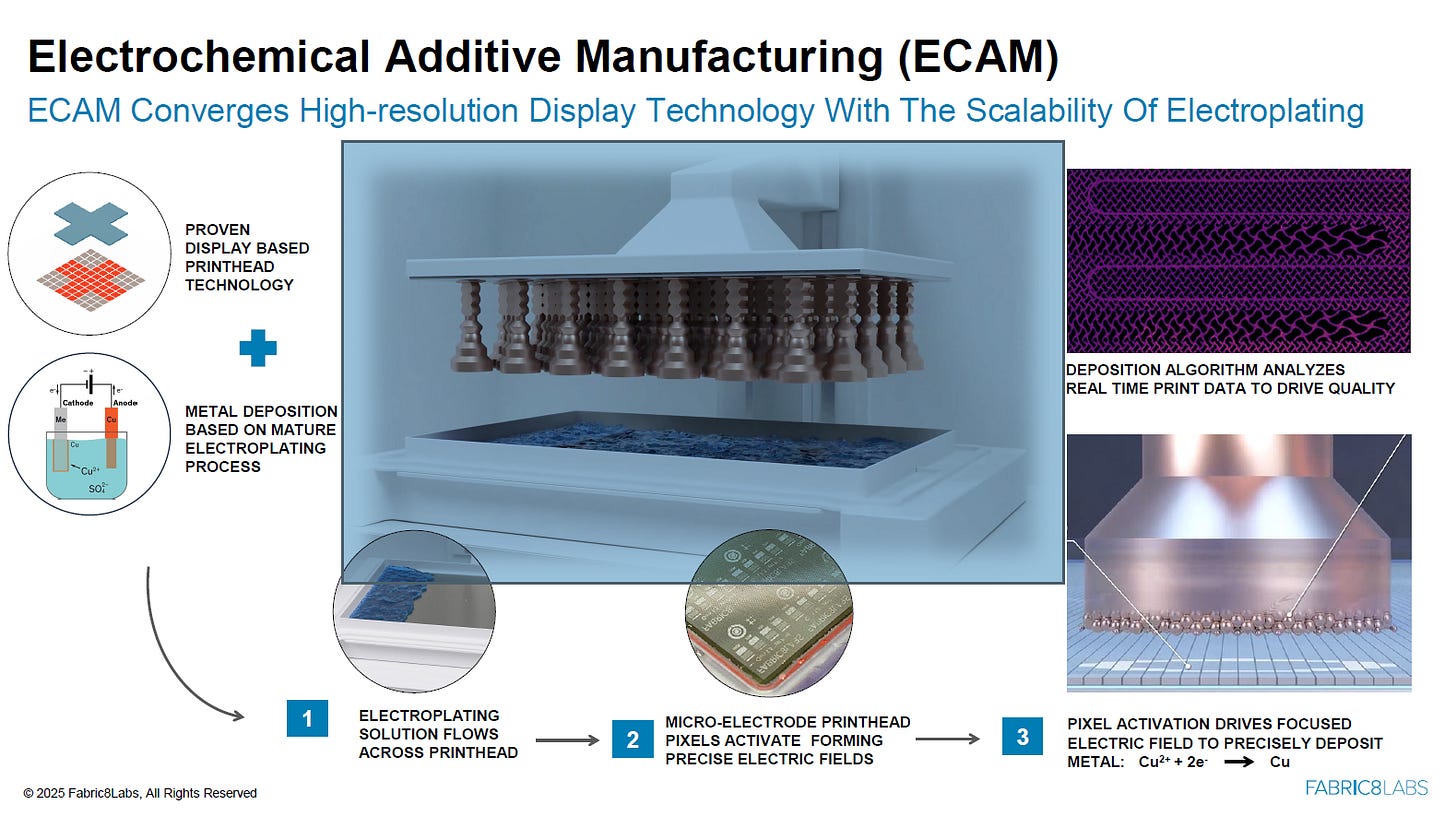
At the2025 Hot Chips conference, an innovative company calledFabric8Labspresented its perspective onmicrochannel technology.
Fabric8Labs Shines at HOT CHIPS 2025
Electrochemical Additive Manufacturing (ECAM) is Reshaping the Future of AI Thermal Solutions
Who is Fabric8Labs?
Fabric8Labs, founded in 2015 and headquartered in San Diego, California, specializes in Electrochemical Additive Manufacturing (ECAM) — an innovative metal 3D printing process that operates at room temperature, uses no powders, and requires no heat sources. This enables direct fabrication of high-purity, micron-resolution, complex metal structures (especially copper), targeting the semiconductor, communications, and thermal management value chains.
In 2023, the company raisedUSD 50 million in Series B fundingfromNEA,Intel Capital,imec.xpand,SE Ventures,TDK Ventures, andLam Capital, among others.
Key Features of ECAM vs. Traditional Metal AM (Powder Bed / Sintering)
Room temperature, aqueous process:Uses metal ion solutions, requires no powder or high-temperature sintering, resulting inlow energy consumptionandbetter sustainability.
Ultra-pure copper (>99.95%): Achievesmicron-scale resolutionand enables fabrication ofcomplex internal geometries.
Geometry-native manufacturing:Complex structures can be printed directly,eliminating most secondary machiningand accelerating production scalability.

Why ECAM is Particularly Suitable for AI Thermal Management
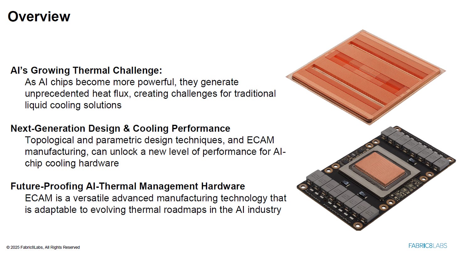
As GPU and accelerator packaging heat flux densities rise rapidly, traditional straight-channel cold plates face performance ceilings due to boundary layer development (which degrades convective heat transfer along the flow path) and erosion limits of copper and fittings (~1.5–2 m/s) when attempting to increase flow velocity.
Fabric8Labs’ ECAM process can directly print offset/slotted microchannels, TPMS (Triply Periodic Minimal Surface) gyroid structures, and capillary/wetting structures, unlocking new levels of performance for single-phase and two-phase cooling.
Moreover, ECAM aligns with theroadmap for pushing liquid cooling deeper into the package:
Fromboard-level cold plates,
Topackage-level liquid-cooled IHS(eliminating TIM2),
Eventually todirect-to-silicon cooling(eliminating TIM1 entirely).
Collaboration with Taiwan: Ecosystem Integration
AtComputex 2025 (Taipei),Fabric8LabsandWiwynn, a leading Taiwanese server manufacturer, jointly showcased ECAM cold plate applications forAI data centersatTaipei Nangang Exhibition Center. The demo combinedFabric8Labs’ advanced thermal structureswithWiwynn’s liquid-cooled rack solutions, marking an importantdeployment signal for ECAM technology within Taiwan’s AI infrastructure ecosystem.
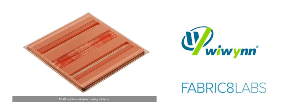
Fabric8Labs:“ECAM Enabled Thermal Solutions for the AI Data Center”
Fabric8Labs’ session focused onpushing the boundaries of microchannel cooling geometry, real-world performance demonstrations, and itsprocess integration roadmap:
1.Microchannel Limits & New Geometries
Problem:Straight microchannels suffer axial heat transfer decay due to boundary layer growth; increasing flow speed is limited by material erosion.
ECAM solution:Enablesoffset/slotted microchannels,finlets, andTPMS (gyroid)geometries toreset boundary layers, enhancing heat transfer and temperature uniformity.

2.Single-Phase Performance
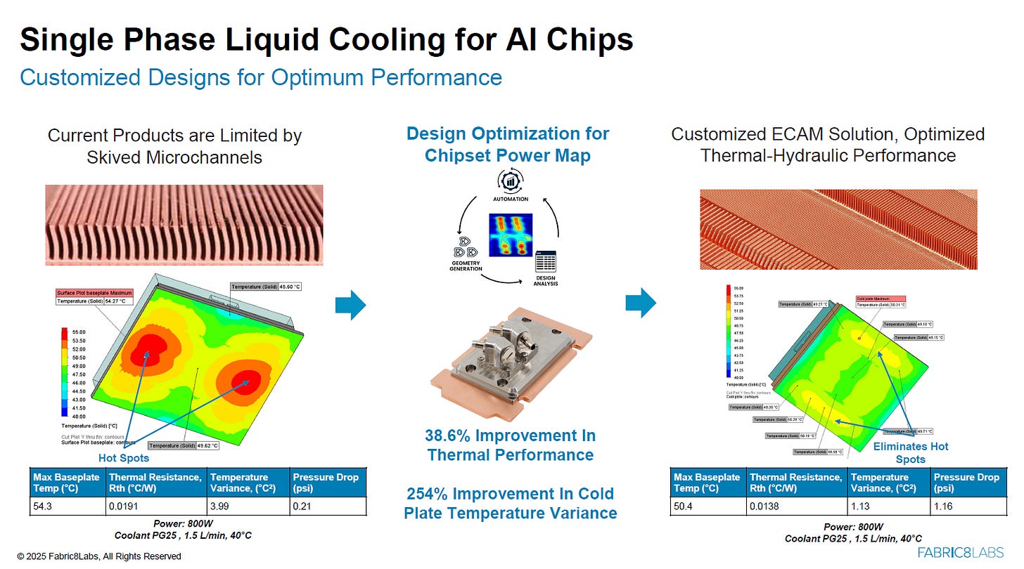
Test condition:800 W, PG25 coolant, 1.5 L/min, 40 °C.
ECAM cold plate vs. traditional skived copper:
Thermal resistance improvement:~38.6%
Temperature uniformity improvement:~254%
Hotspot suppression: Significant
Pressure drop remained similar (~1.16 psi).
3.Two-Phase Enhancement

Capillary/wetting structuresprinted via ECAM improve liquid return and dry-out resistance.
TheRth–power curvefor two-phase cooling shows lower thermal resistance maintained even at high TDP.
Immersion boiling surfaces with3D lattice and protrusionsshowed reduced CPU junction temperatures in400 W TDPtests.

4.Process & Integration Roadmap
Board-level cold plates → liquid-cooled IHS (TIM2 removal) → direct-to-silicon (TIM1 removal).
Demonstratedwafer-scale copper printingandEDA/power-map driven geometric optimization, pointing towardchip-level thermal structure integration.
Public Collaborations
Asetek (Denmark):Announced an exclusive partnership with Fabric8Labs to combineECAMwithAI-optimized algorithmsfor next-generation cold plate geometries, targeting bothcommercialandconsumer desktopliquid cooling markets.
Microchannel Cooling Innovation: From Machining to ECAM
Background: Thermal Challenges in the High Heat Flux Era

Themicrochannel cooling concept, pioneered byTuckerman and Pease at Stanford in 1981, demonstrated the ability to handle~800 W/cm²under single-phase liquid cooling. With rising AI chip power, this technology has become central tohigh-performance cooling research.
Advantages of Microchannel Cold Plates
High thermal performance:Thermal resistance as low as0.07 K/Wunder single-pass flow.
Compact size:Volume ~11.2 cm³ vs. ~500 cm³ for air coolers.
Low pumping power:Due to dense channels and laminar flow.
Limitations of Conventional Microchannels
Boundary layer growthreduces local heat transfer coefficients along the channel.
Pressure drop and erosionlimit flow velocity scaling.
Fouling and dry-outreduce reliability over long-term operation.
Geometry and Flow Innovations
Inclined / segmented fins,convergent-divergent channels with ribs,wavy or serrated paths, andmicrostructures(pillars, cavities) can significantlyreinvigorate boundary layers,enhance secondary flow, andboost heat transfer.
Normal-flow microchannelscan achieve0.02 °C·cm²/Wwith low pressure drop.
Two-phase flow strategiessuch asforce-fed boilinguse microgrooves to sustain high critical heat fluxes.
Manufacturing Techniques and ECAM Breakthrough
Conventional microchannel manufacturing—skiving,CNC milling,chemical etching,EDM, ormicro-deformation—faces limitations ingeometric complexity,throughput, andcost.
ECAM, however, enables:
High-resolution, pure copper microstructuresprinted directly onto substrates.
Integration on silicon, ceramics, or foilswithout thermal stress.
Generative AI–driven designssuch asgyroidsandoffset microchannelsto optimize thermal paths.
20–30% improvement in thermal performance,20–40% lower pressure drop, and60–85% better temperature uniformityover conventional designs.
Future Roadmap
Current:Board-level ECAM cold plates, improving fin/channel geometry, reducing thermal resistance by 20–50%.
2026–2027:Package-level liquid cooling, integrating ECAM structures within the package (no TIM2), expected 30–40% further thermal resistance reduction.
2028 and beyond:Direct-to-siliconECAM fins and channels inside the chip package, fully eliminating TIM1 and TIM2, targetinganother 30–40% reductionin thermal resistance.
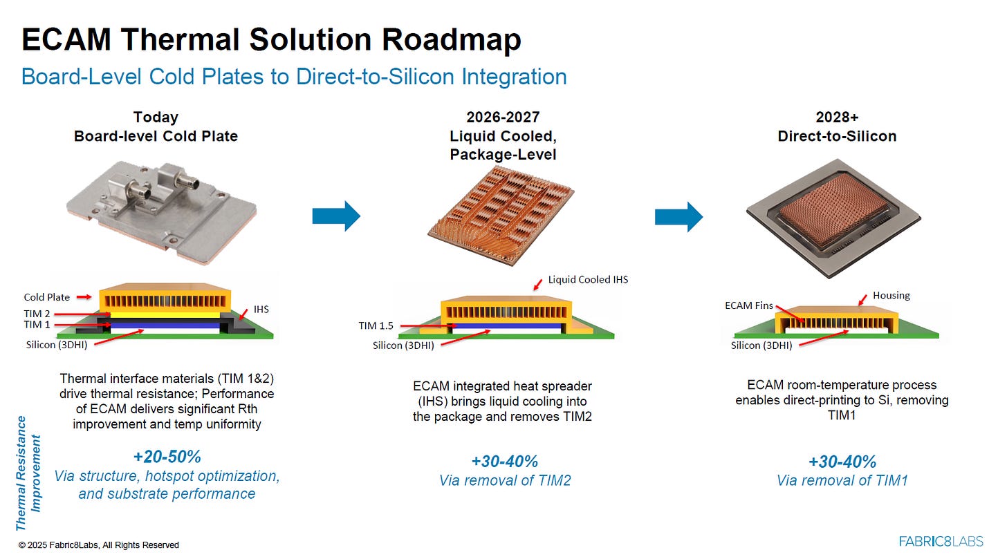
Microchannel cooling remains a key enabler for high-power-density electronics, but conventional manufacturing faces limits. By changing channel geometries, adding turbulence structures, leveraging two-phase cooling, and especially adopting ECAM, the thermal resistance and hotspot problems can be fundamentally improved.
With ECAM and generative design, thermal structures can be directly integrated into the package or even the silicon, marking a paradigm shift. As fabrication methods mature, microchannel-based solutions will play a central role in AI, data centers, and high-power electronics for years to come.
Another cooling solution… xMEMS?
xMEMS Labs, Inc.(xMEMS) is a company specializing inMEMS (Micro-Electro-Mechanical Systems)technology, with a core platform based onpiezoMEMS (piezoelectric MEMS)andsingle-crystal siliconprocessing.

Originally, xMEMS focused onMEMS audio speakersandacoustic vents, but after establishing a footprint in the audio sector, it beganextending its MEMS platform to thermal management, usingpiezoelectric vibration to drive micro-airflowforactive cooling.
This new class of device is referred to as“µCooling fan-on-a-chip”or“active µCooling.”
On its official website, xMEMS describes itself as the“world’s most innovative piezoMEMS silicon platform”, highlighting applications inMEMS speakers,active micro-cooling, andacoustic ventilation.

xMEMS µCooling / Fan-on-a-Chip Thermal Solutions
1.Product Overview & Key Specifications
TheXMC-2400 µCooling chipis xMEMS’s flagship thermal management device and is theworld’s first 1 mm-thick, all-silicon, solid-state fan-on-a-chip.
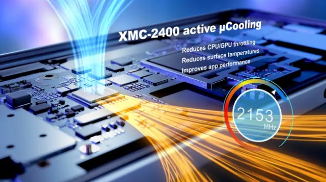

- Operating Principle
TheµCooling chip uses a piezoelectric MEMS structureconsisting of a vibratingmembrane and micro-channelsetched into a silicon die. When actuated atultrasonic frequencies, the membrane generatespressure pulsesthat drive airflow — unlike traditional rotary fans with blades and bearings.
Because the device isextremely thin and can be integrated at the chip or package level, it enablesactive cooling in ultra-space-constrained environmentssuch assmartphones,tablets, andSSDs.
In practice, µCooling modules are often combined withheat spreaders, vapor chambers, or thermal interface materials, allowing the generated airflow to efficiently remove heat from localized hotspots.
3.Applications and Demonstrations
xMEMS has demonstrated or announced µCooling applications in multiple domains:
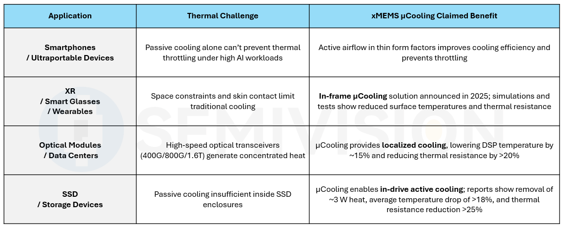
Media such asPCWorldhave noted xMEMS as apotential next-generation SSD cooling competitor to Frore’s AirJet, withsmaller size and greater integration flexibility.
4.Launch Timeline, Mass Production Plans, and Milestones
2025: xMEMS announced µCooling expansion tooptical transceiver applicationsin data centers.
May 2025: µCooling forSSD applicationsunveiled, with thermal models and performance projections.
Sensors Converge 2025:XMC-2400 µCoolingawarded“Best MEMS Solution.”
2026 (planned): Sampling and mass production ramp, focused onXR/smart glasses,SSD modules, andoptical modules.
Advantages, Challenges, and Future Directions
Advantages
Ultra-thin, easily integrated: ~1 mm thickness allows embedding in phones, glasses frames, SSDs — unlike conventional fans or blowers.
Solid-state, long lifetime: No bearings or moving parts; piezoelectric actuation offers high durability.
Low power, silent operation: Tens of milliwatts; ultrasonic actuation is inaudible to humans.
Modular & scalable: Multiple µCooling units can be arranged or stacked to increase flow/pressure; supports bi-directional airflow.
Hyper-localized cooling: Targets hotspots that passive cooling cannot reach (e.g., SSD controllers, DSP chips).
Challenges and Limitations
Airflow / pressure vs. heat flux: µCooling cannot match the absolute thermal capacity of large fans or liquid cooling — better suited as asupplementary, not primary, solution for high-TDP systems like GPUs.
Thermal path design complexity: Requires thoughtful integration with heat spreaders and ducts to effectively remove heat. Poor system design may reduce its impact.
Cost & manufacturing maturity: While silicon-based,volume production, packaging, and reliability qualification(e.g., temperature cycling, humidity, contamination) are still underway. Mass production is expected around2026.
Integration & standardization: OEMs/ODMs must handle air inlet/outlet design, sealing, filtering, and airflow control (e.g., I²C interfaces), which adds system integration work.
Thermal limits: µCooling alone may not handleextreme heat fluxes or thick thermal resistances, requiring hybrid solutions (e.g., vapor chambers, microchannels, liquid cooling).
Future Directions and Opportunities
3D thermal architectures: Combining µCooling with microchannels, fins, or heat pipes for multi-mode cooling.
Smart control: Integrating sensors and dynamic airflow control to optimize energy and noise.
Package-level integration: Embedding µCooling directly above SoCs or within wafer stacks for ultimate localized cooling.
Expanded applications: Autonomous driving ECUs, drones, edge AI, IoT sensors, and cameras are potential markets.
Ecosystem collaboration: Partnerships with SSD vendors, optical module makers, mobile and wearables OEM/ODMs are key to commercialization.
xMEMS’s µCooling fan-on-a-chip represents a new class of solid-state active cooling, leveraging piezoMEMS technology to address thermal challenges in ultra-thin, localized, and integration-sensitive environments. While not a replacement for high-capacity cooling systems, its scalability, silence, and integration flexibility make it a promising complementary technology for next-generation AI devices, data center modules, and wearables — with mass production targeted for 2026.


PreviousNext
TopLatestDiscussions








See all