TSMC: Acceleration of Taiwan’s “Local-to-Local” Semiconductor Strategy
TSMC: Acceleration of Taiwan’s “Local-to-Local” Semiconductor Strategy
- Source: SemiVision
- Author: SEMIVISION
- Published: 2025-09-25T20:22:08+08:00
- URL: https://tspasemiconductor.substack.com/p/tsmc-acceleration-of-taiwans-local TSMC: Acceleration of Taiwan’s “Local-to-Local” Semiconductor Strategy


TSMC: Acceleration of Taiwan’s “Local-to-Local” Semiconductor Strategy
Original Articles By SemiVision Research (SEMICON, TSMC, ASE, PTI, Corning, Besi, K&S, ASMPT, Globalfoundries, Onto, DISCO, Henkel, Globalwafers, KINK)

Sep 25, 2025
∙ Paid

At this year’s SEMICON Taiwan 2025 Technology Forum, AI/HPC was once again reaffirmed as the central driver behind the evolution of semiconductor manufacturing, advanced packaging, and testing technologies. The core discussions focused on CoPoS, 3D hybrid bonding, N2 and GAA processes, paradigm shifts in testing, and CPO.

2025年4月22日
First, CoPoS (Chip-on-Panel-on-Substrate) remains in the pilot production and validation stage. While TSMC has already confirmed the 310×310 mm panel substrate size, the overall ecosystem is still immature. A realistic timeline for volume production is closer to 2029–2030. At the same time, 3D hybrid bonding is shaping a blueprint for so-called “3.5D packaging.” Both AMD and Broadcom have showcased real-world deployments, and TSMC’s SoIC platform is set to expand further, driven by large customers such as Apple and Meta. However, short-term visibility for equipment orders is lower than expected.
On the logic process and materials innovation side, TSMC confirmed that N2 will enter mass production in 2025, with roadmaps advancing toward A16 with backside power delivery and the A14 node, emphasizing the importance of DTCO/STCO co-design and Ångström-level precision control. In parallel, the testing industry is undergoing a value reassessment: as chip size and complexity continue to grow, “Shifting Left” in testing is becoming the new standard. TSMC and ecosystem partners showcased advanced probing solutions and AI-assisted approaches.

Finally, Bizlink used the exhibition to highlight its entry into new domains such as CPO and semiconductor process equipment (SPE). Partnering with SENKO and ficonTEC, Bizlink is gradually becoming part of TSMC’s CPO supply chain, evolving from cable manufacturing to full-system integration — underscoring its strategic transformation and growth potential.

2025年4月15日
Overall, SEMICON Taiwan 2025 sent a clear signal: as AI/HPC drives ever-larger die sizes and compute demands, the value of packaging, testing, and optical interconnects will rise sharply, with Taiwan’s supply chain actively investing in new technologies to navigate this structural transformation.

Acceleration of Taiwan’s “Local-to-Local” Semiconductor Strategy:
Materials Self-Sufficiency, Localization of Advanced Packaging, and the Kickoff of CoPoS

2025年9月16日
In recent years, geopolitical risks in the global semiconductor industry have continued to rise, making supply chain security no longer a back-end consideration but a core element of strategic planning. As a global semiconductor hub, Taiwan made a clear statement at SEMICON Taiwan 2025 through its “Local-to-Local” policy: the future strategy is not only to consolidate its leading position in wafer manufacturing but also to comprehensively expand in three critical areas—materials self-sufficiency, localization of advanced packaging, and acceleration of CPO/CoPoS platforms—in order to build a complete and resilient local ecosystem.

At SEMICON Taiwan 2025, the technical forum once again delivered a clear message: AI and HPC are redefining the core driving forces of the semiconductor industry. As generative AI, inference, and training workloads continue to expand, the scale of model parameters is rapidly leaping from tens of billions to the trillion level. The compute density and power consumption of a single GPU/AI accelerator have already surpassed the kilowatt-class threshold, while memory bandwidth requirements have broken through 10 TB/s. This is forcing a profound restructuring across the entire supply chain—from front-end wafer manufacturing to back-end packaging and testing.
The forum highlighted critical paths that will shape the competitive landscape of the next decade: CoPoS (Chip-on-Panel-on-Substrate), 3D Hybrid Bonding, N2 and GAA nodes, paradigm shifts in testing, and CPO (Co-Packaged Optics) integration.
In advanced process technology, the N2/GAA rivalry between TSMC and Intel is not only about yield and transistor density, but also about whether future system architectures can sustain the massive data throughput required for AI workloads. In packaging, 3D Hybrid Bonding and the expansion of CoWoS/FOPLP have become strategic cornerstones for integrating HBM, SerDes, and GPU/AI ASICs. Meanwhile, panel-level CoPoS packaging represents liberation from reticle limits, enabling ultra-large-area interconnects and cost-efficient, high-volume solutions.
In testing and inspection, traditional electrical testing methods are no longer sufficient to handle the complexities of electro-optical heterogeneous integration, driving adoption of optical metrology, adaptive test platforms, and AI-driven defect analytics as new standards. On the system interconnect front, the rise of CPO and OIO (Optical I/O) directly challenges the physical limits of copper. By co-packaging optical engines with ASICs, they can cut long-distance SerDes losses, deliver ~3.5× energy-efficiency gains, and bring a revolutionary shift to data centers and supercomputing clusters.
Taiwan plays a pivotal role in this structural transformation. Historically, Taiwan’s global semiconductor position was anchored by wafer manufacturing (with TSMC at the core). Today, however, its strategic footprint extends across the entire supply chain. Through a “Local-to-Local” localization strategy, Taiwan is strengthening self-sufficiency in upstream materials such as EUV photoresists, photomasks, chemicals, CMP consumables, and wet process chemicals—reducing reliance on single international suppliers and building diversified supply networks to mitigate geopolitical risks.

At the same time, advanced packaging capacity is expanding rapidly. Industry leaders such as TSMC, ASE, and Powertech are scaling platforms including CoWoS-S, CoWoS-R, InFO, FOPLP, and SoIC-X, building new facilities in Kaohsiung, Taichung, Hsinchu, and Central Taiwan. These are being integrated with liquid cooling, microfluidic thermal solutions, and 3D integrated testing to form a complete AI/HPC packaging cluster.

2025年3月3日
In photonics, Taiwan is co-developing CPO and OIO platforms with NVIDIA, Broadcom, Marvell, while also attracting optical connector and FAU players such as Bizlink, FOCI, Teramount, and Senko to set up locally. Combined with academic institutions like ITRI, NCTU, and NCKU, Taiwan is gradually forming a silicon photonics and optoelectronic packaging cluster.

2025年4月12日
Going further, the Taiwanese supply chain is evolving from pure contract manufacturing to vertical collaboration across design–manufacturing–testing–packaging–materials. Through co-design (DTCO, STCO), EDA platforms, and advanced testing services, Taiwan is constructing a comprehensive strategic fortress spanning materials, equipment, process, packaging, and photonic integration.
This means Taiwan is no longer just the global hub for wafer manufacturing—it is also becoming the core node for next-generation AI infrastructure, optical interconnects, and heterogeneous integration platforms, with an irreplaceable strategic role. In other words, Taiwan will serve as a dual engine for both Moore’s Law extension (advanced nodes) and Beyond-Moore innovation (packaging and photonic integration), ensuring its continued leadership in the global AI/HPC era.

For Paid Members, SemiVision will discuss topics on
Materials Self-Sufficiency: Tackling the Bottlenecks First
Localization of Advanced Packaging: Dual-Track Expansion in Capacity and Equipment
CPO / CoPoS Takeoff: Building the Next-Generation Platform
From Slogan to Execution: Taiwan’s New Semiconductor Strategy
Semicon Taiwan’s Silicon Photonics Forum and the Road Ahead
GlobalFoundries’ Fotonix Platform
New Highlights and Trends Observed at Semicon Taiwan
Future Directions and Key Opportunities
PTI and ASE in FOPLP: Strategies and Key Technologies
PTI’s FOPLP Development Focus
ASE’s Commitment and the VIPack™ Platform
The Relationship Between FOPLP and Optical Engines
AGC: Applications for Glass-core substrate
Senko: Expanded Beam , Detachable connectors for CPO
COMET :3D X-ray solution for 3D Packing
Heterogeneous Integration Tech Forum : Glass Core / Glass Substrate Supply Chain and Technical Perspectives
3D X-Ray Inspection / Comet Yxlon’s CA20 System and Advanced Testing Needs
Why 3D X-Ray Is Critical in FOPLP / Advanced Packaging Environments
Corning’s Strategy in Glass Materials and Applications in Glass Substrate / Glass Core
How Glass Substrate / Glass Core Are Applied (Integration with FOPLP / Advanced Packaging)
Semiconductor Supply Chain Driving Next-Generation Advanced Packaging
Semiconductor Supply Chain Driving Next-Generation Advanced Packaging (KINK &PSI)
Process Equipment: Extending Front-End to Back-End (LAM & TEL & SCREEN )
Bonding and Packaging: The Core Driver of Interconnect (EVG & BESI & ASMPT & HANMI & K&S)
Metrology and Inspection: Guardians of Yield (ONTO & DISCO & Lasertec )
Company Updates / SEMICON Taiwan Highlights (SUSS MicroTec & Advantest & TEL)
Materials / Supply Chain & Overall Exhibition Trends
Local Supply Chains Driving the Infrastructure for Advanced Packaging (G2C+ & KINK )
A New Chapter in Advanced Packaging for the Chiplet Era
EVG and Hybrid Bonding Leadership
Fluxless TCB and D2W Hybrid Bonding Expansion
Market Outlook: Dual-Track Competition
Core Technical Challenges & Future Watch Points
Henkel’s Material Strategy and Advanced Packaging Reliability for AI Chips
Inspection and Testing: The Quality Safeguard of Advanced Packaging
Inspection & Testing Supplier Landscape and Trends
Breakthrough in Silicon Photonics Testing: Double-Sided Testing as a New Benchmark for PIC/EIC Reliability (FiconTEC)
Key Highlights of GlobalWafers’ 12-inch SiC Wafer Technology
The Next Frontier of Chip Technology: Radical Innovation for Unprecedented Performance
Diamond on Chip: A Revolution in Thermal Management
Comparative Analysis of Next-Generation AI Accelerator Specifications
National Strategy and Industry Response
SemiVision believes that the strategic significance of CPO is driving the acceleration of the optical interconnection industry with unprecedented force. In AI/HPC application scenarios, traditional copper interconnects are reaching both physical and energy-efficiency limits: high-speed SerDes, when transmitting across packages or modules, must rely on compensating circuits such as retimers, equalizers, and pre/post-emphasis to maintain signal integrity (SI). However, these solutions come at the cost of high power consumption and latency, making it increasingly difficult to sustain improvements in energy per bit (pJ/bit) and bandwidth density (Gbps/mm). This is precisely why Optical I/O has become an inevitable choice.
Optical interconnects offer inherent physical advantages such as low loss, multi-wavelength parallelism (WDM), and long-distance transmission. More importantly, through the deep integration of Co-Packaged Optics (CPO) and optical engines, optical coupling points (the “beachfront”) can be placed closer to the ASIC die edge, reducing electrical distance and dramatically lowering insertion loss. This elevates bandwidth density to the Tb/s per mm level while significantly reducing power consumption.
Yet, for Optical I/O to truly deliver higher bandwidth and lower power, the optical engine itself must be tightly coupled with advanced packaging technologies—no longer as a standalone pluggable module, but as a system-level integration that unifies circuits, power delivery, and cooling. This is why we see rapid evolution in packaging interconnect technologies: from conventional micro-bump/solder-based packaging, progressing toward fluxless TCB (thermo-compression bonding without flux) and hybrid bonding (Cu-Cu or metal/dielectric hybrid bonding), and extending further to FOPLP (fan-out panel-level packaging) and TGV (through-glass via) platforms.
Fluxless TCB is valuable for eliminating flux residue, improving interfacial purity, and maintaining bonding reliability as pitch shrinks—acting as a transitional solution toward hybrid bonding. Hybrid bonding, with its sub-10 µm pitch interconnect capability, ultra-low contact resistance, and 3D IC integration potential, has become the core technology for future high-density heterogeneous integration. However, it imposes extremely stringent requirements for surface planarity, cleanliness, and alignment precision, raising the technical bar for both OSATs and equipment vendors.
Meanwhile, FOPLP and TGV technologies point toward larger-area packaging modes. Glass substrates, with their low dielectric constant (low-k), low CTE, and high dimensional stability, combined with vertical vias, enable higher I/O integration, paving the way for substrate solutions to support ultra-large AI modules.
The common driving force behind all these evolutions is the skyrocketing power density and heat flux density of AI accelerators. Single GPUs are approaching—or even exceeding—the kilowatt power threshold, while localized heat fluxes surpass the limits of traditional cooling. As a result, microchannel and microfluidic cooling are becoming unavoidable. These microchannels must be built directly into the package, interposer, or even RDL layers, reducing the thermal path to tens of microns, significantly lowering thermal resistance, and maintaining performance stability. However, this also introduces new challenges in pressure drop control, packaging hermeticity, and materials compatibility.
Thermal/electrical co-design issues are tightly linked with power integrity (PI) and signal integrity (SI). AI GPUs require PDNs capable of delivering thousands of amps of current, making IR drop, Ldi/dt noise, and target impedance design stricter than ever—and inseparably intertwined with the SI of high-speed SerDes. This is why future packaging design must move toward holistic PI/SI/Thermal/Optical co-design, rather than optimizing each domain in isolation.

2025年8月10日
Testing and characterization challenges are also escalating. Traditional electrical probing is insufficient for optoelectronic heterogeneous integration. FAU (fiber array unit) and coupling technologies are now central: 2D FAU, 3D FAU, and sub-micron alignment must ensure low insertion loss, low reflection, and long-term stability under thermo-mechanical stress. Test platforms are evolving into double-sided electro-optical probing, combining GHz-level electrical testing with optical dimensions such as BER/eye diagrams, polarization mode dispersion (PMD), coupling loss, dispersion, and nonlinearities—driving up the complexity of test equipment and data analysis.
2025年6月2日
This means design teams must transcend traditional boundaries between chip design, packaging engineering, thermal engineering, photonics, and test engineering, engaging in cross-domain collaboration from the earliest stages. Future AI chips will not merely be semiconductors, but system-level multi-physics integration platforms—with design complexity and supply chain depth far exceeding that of the traditional wafer fabrication era.

2025年9月21日
Materials Self-Sufficiency: Tackling the Bottlenecks First
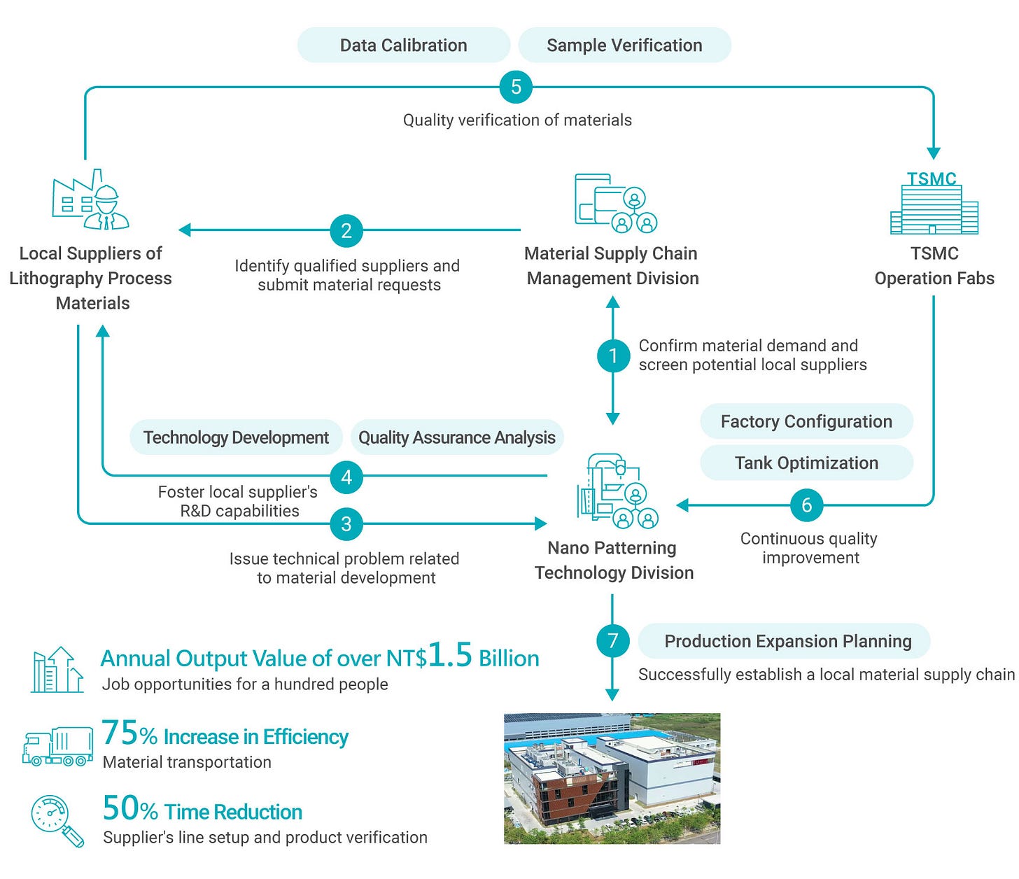
Taiwan has long relied on imports of high-end semiconductor materials, particularly EUV photoresists, specialty gases, and chemicals and adhesives required for advanced packaging. However, once these supply links are constrained by international policies or sudden disruptions, production lines are directly impacted.
To address this vulnerability, leading companies have begun driving materials localization. TSMC, for example, introduced an “innovative business model” in collaboration with suppliers to establish Taiwan’s first EUV photoresist factory, securing one of the most fragile links in advanced manufacturing. This move not only strengthened local production security but also paved the way for further material localization, such as high-purity IPA, etching gases, RDL chemicals, and TIM adhesive materials—gradually reducing dependence on imports.
Localization of Advanced Packaging: Dual-Track Expansion in Capacity and Equipment
Driven by the wave of AI and HPC, advanced packaging has become a critical battleground in global semiconductor competition. At and around SEMICON Taiwan, both industry and government released strong signals of support, explicitly designating CoWoS and Fan-Out packaging as strategic priorities.
Taiwan is already the world’s primary production hub for CoWoS, with industry estimates suggesting that monthly capacity could double to 80,000 wafers by the end of 2025, and potentially reach 100,000 wafers per month in 2026. This expansion is not merely about capacity but also about deepening technology—progressing from 2.5D and 3D IC to panel-level packaging (FOPLP), and further toward integrating HBM and high-bandwidth AI GPU modules.
At the same time, the domestic supply chain for equipment and materials has begun achieving self-sufficiency. Localized production now covers SiC substrates, CMP consumables, X-Ray/TSV inspection tools, and more. Step by step, Taiwan is building a comprehensive local ecosystem for advanced packaging, reducing its reliance on foreign equipment and reinforcing supply chain resilience.
CPO / CoPoS Takeoff: Building the Next-Generation Platform
As AI data centers face escalating challenges of power consumption and bandwidth, traditional copper interconnects are reaching their physical limits, making optoelectronic integration the inevitable solution. At SEMICON Taiwan’s forums and keynote sessions, CPO (Co-Packaged Optics) and CoPoS (Chip on Panel on Substrate) were identified as critical directions for the future.
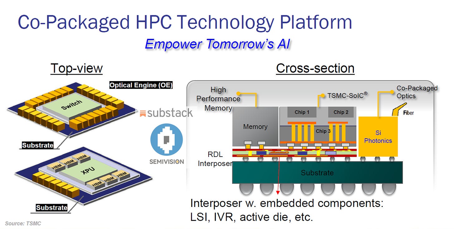
Taiwan’s ecosystem is uniquely positioned to accelerate this transition. With mature SerDes design capabilities, advanced packaging capacity, and strong system integration know-how, Taiwan can vertically integrate the entire chain—from optical engines to optical packaging to switching modules. This marks a shift: CPO and CoPoS are no longer confined to laboratory demonstrations but are entering the crucial stage of pilot programs and scaling toward mass production. Closer collaboration between academia and industry, alongside international supply chain partnerships, will strengthen Taiwan’s indispensability in the next generation of AI/HPC infrastructure.
From Slogan to Execution: Taiwan’s New Semiconductor Strategy
Taiwan’s “Local-to-Local” approach is not a mere slogan but a top-down, end-to-end execution roadmap:
Production Line Validation:SEMICON Taiwan serves as a platform to bring new requirements directly into testing and adoption stages.
Localized Materials:Step-by-step establishment of domestic capacity for EUV photoresists, specialty chemicals, and gases.
Equipment Deployment:Attracting international equipment vendors to set up local operations, creating a Taiwan-centered procurement chain.
Packaging Scale-Up:Expanding CoWoS, FOPLP, and other advanced packaging capacities to solidify Taiwan’s global leadership.
Optoelectronic Integration:Driving CPO and CoPoS initiatives to build the next generation of high-speed, low-power computing platforms.

Semicon Taiwan’s Silicon Photonics Forum and the Road Ahead
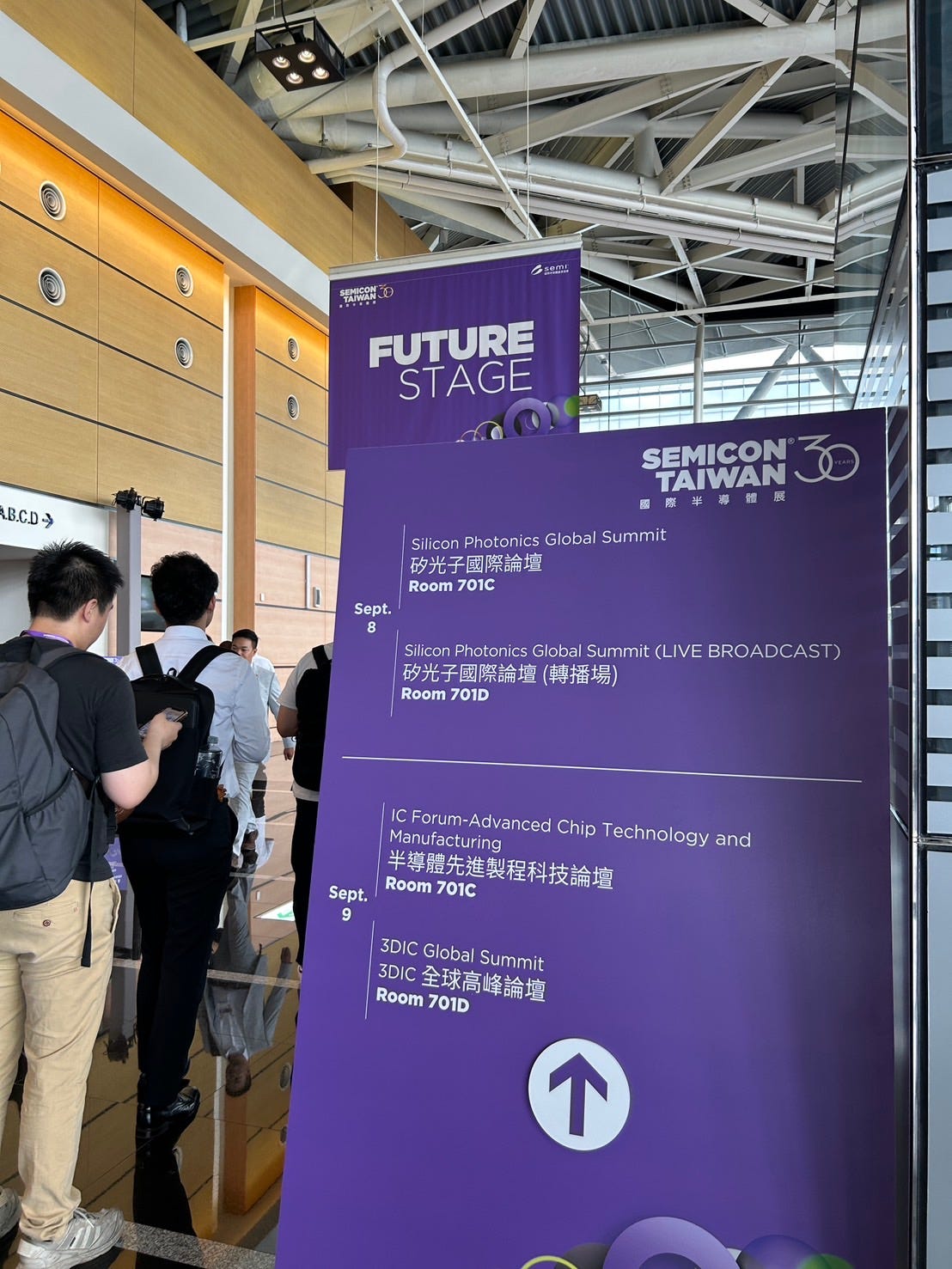
Semicon Taiwan concluded successfully today, wrapping up a week filled with cutting-edge discussions and technology showcases. Across sessions on FOPLP, advanced logic, 3D IC, advanced testing, compound semiconductors, and the dedicated silicon photonics forum, experts and industry leaders gathered to share insights. Among these, silicon photonics stood out as one of the most anticipated topics. Its rapid progress not only signals a breakthrough in overcoming bandwidth and power bottlenecks but also marks a new stage in semiconductor manufacturing and optoelectronic integration.

Technology and Platform Landscape
TSMC’s COUPE Platform
At the Silicon Photonics Global Summit, TSMC highlighted its COUPE (Compact Universal Photonic Engine) platform, positioned as a next-generation optical interconnect solution tailored for servers and AI/HPC systems.
The core advantage of COUPE lies in its ability to integrate optical and electrical transmission, enabling dense data transfer through Wavelength Division Multiplexing (WDM) on a single fiber. Compared with traditional electrical connections, this approach can drastically reduce the number of cables and connectors, while lowering power consumption and mitigating heat dissipation challenges.
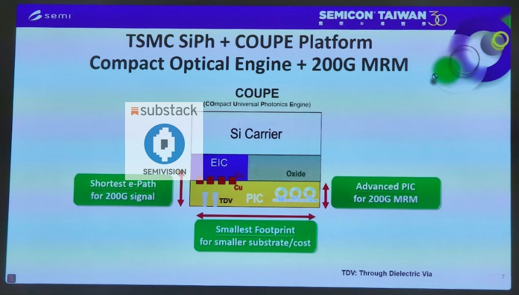
From a design perspective, TSMC emphasized that cross-domain integration between PICs (Photonic Integrated Circuits) and EICs (Electrical Integrated Circuits)—whether through co-integration/co-packaging or monolithic integration—remains one of the key technical hurdles. Ensuring alignment, reliability, and yield between optical components (waveguides, modulators, detectors) and electronic circuits (high-speed drivers/receivers, power management) will be central to the COUPE platform’s long-term success.
GlobalFoundries’ Fotonix Platform
GlobalFoundries’GF Fotonix™is one of the company’s flagship technology platforms for silicon photonics, combining high-performance active photonic devices with low-loss passive components to meet the growing demands of data centers, high-frequency communications, and optical interconnects.
The platform is designed to deliverhigh bit rates and bandwidth density over a single optical fiber, while minimizing both power consumption and signal loss. Passive components—such as waveguides, multiplexers, and splitters—are engineered to achieve extremely low insertion loss and strong stability. Meanwhile, active components—including modulators and photodetectors—are optimized for high speed, low drive voltage, and excellent electro-optical modulation efficiency.

To strengthen its ecosystem, GF has partnered with tool providers such asAnsys Lumerical, certifying its design toolkit so that engineers can leverage advanced photonic solvers to simulate and validate both individual devices and complete systems on the Fotonix platform. This integration is critical forshortening design cyclesandreducing failure risks, ensuring faster time-to-market for photonic-enabled applications.
Global Players and Emerging Trends
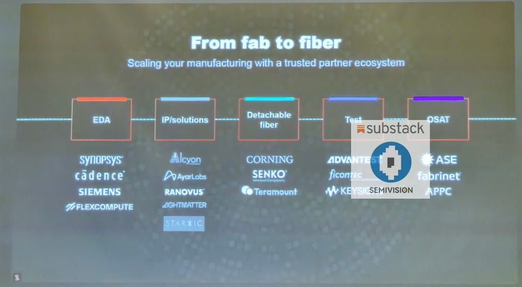
Beyond TSMC and GlobalFoundries, other major players such asIntelandTower Semiconductorhave also invested heavily over the years in the research, development, and commercialization ofsilicon photonics (SiPh)technologies.
In Taiwan, industry initiatives are also taking shape. The establishment of theSilicon Photonics Industry Alliance (SiPhIA), with over 30 companies participating, reflects a strong push to integrate the supply chain and accelerate ecosystem development.
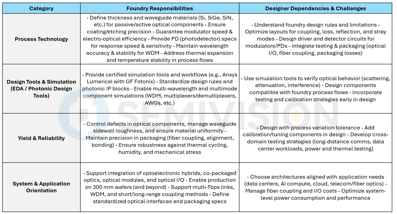
The Critical Role of Foundry vs. Design/Process Know-How
In silicon photonics, thedesign rules and process know-how provided by foundriesare crucial to enabling designers to quickly develop and successfully commercialize products. The division of roles and challenges can be summarized as follows:
New Highlights and Trends Observed at Semicon Taiwan
“Awakening Year” for Silicon Photonics
TSMC executives described2024 as the “awakening year” for silicon photonics, signaling that both the technology and the market have reached a critical inflection point. Demand is now entering an explosive growth phase, underscoring that silicon photonics is moving beyond niche research into mainstream adoption.
Photonics–Electronics Co-Integration / Monolithic Integration
The focus is no longer just on building standalone PICs (Photonic Integrated Circuits). Increasingly, the industry is emphasizingco-integration of PICs with electronic componentssuch as drivers, amplifiers, and ADC/DAC units. This hybrid or monolithic approach reduces latency, lowers power consumption, shortens signal propagation distances, and simplifies overall system complexity and cost. Many leading foundries are directing their R&D efforts toward this integration challenge.
Multi-Wavelength (WDM) and High Bandwidth Density
To achieve higher data throughput on a single optical fiber or channel,WDM (Wavelength Division Multiplexing)has become the standard approach. TSMC’sCOUPE platformpositions WDM as a key enabler, allowing dense multiplexing of optical signals to deliver massive bandwidth without increasing fiber count.
Maturing Toolchains and Ecosystems
Collaboration is accelerating across the industry. Alliances such asSiPhIAare forming to connect the dots between design, testing, packaging, and manufacturing. Foundries are now offeringcertified simulation tools, photonic IP blocks, and well-defined design rulesto ensure that designers can confidently adopt silicon photonics. This maturing ecosystem significantly lowers the entry barrier for new participants.
Application Drivers: AI, Data Centers, and HPC
The strongest pull for silicon photonics comes fromdata centers and AI workloads, where ultra-high-speed, low-latency, and high-bandwidth I/O is essential. As AI models grow larger and training/inference requires more data movement,optical interconnects are emerging as the critical solution to copper bottlenecks. At Semicon Taiwan forums, these application scenarios—ranging from AI clusters to HPC systems—were repeatedly emphasized as the core market drivers.
Manufacturing Challenges: Yield, Stability, and Packaging
While laboratory-level performance of photonic devices has advanced rapidly,scaling into high-volume manufacturing introduces new hurdles. Achieving consistent yield, long-term stability, low-cost fiber coupling, and packaging that can withstand heat, humidity, and mechanical stress are all critical bottlenecks. Multiple speakers at the forum highlighted these pain points, reinforcing that solving manufacturing and reliability challenges will determine how quickly silicon photonics scales to mass deployment.
Future Directions and Key Opportunities
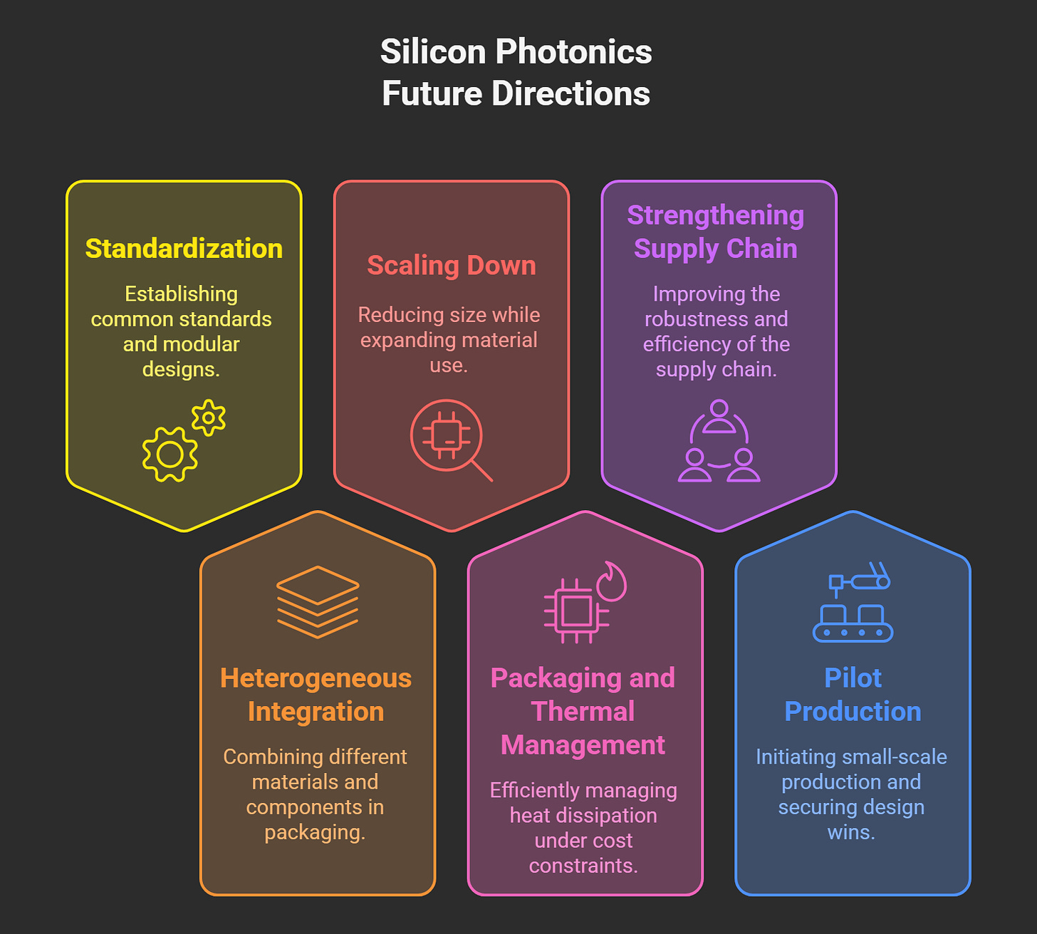
Based on the current state and emerging trends, I believe that over the next one to three years, silicon photonics in Taiwan and the global market will likely evolve and accelerate along the following trajectories:
Standardization and Modularization
Similar to electronic ICs, optical transmission and optoelectronic conversion components will increasingly bemodularized and offered as IP blocksfor repeated use by designers.
Standardization of fiber coupling, packaging interfaces, and packaging processes will be essential tolower system costs and enhance reliability.
Heterogeneous Integration and Co-Packaging
Mixed integration between electronic and photonic chips will gain traction—for example, placing driver circuits and modulators in extremely close proximity to reduce latency and power consumption.
Co-packaged optics (CPO)will become mainstream, integrating photonic and electronic chips in the same module, and potentially incorporating thermal management and power delivery functions.
Scaling Down and Broadening Materials Adoption
Moving from mature nodes (e.g., 65nm, 90nm) towardadvanced process nodes(such as N7, N5, or beyond) to achieve smaller geometries and higher integration density. Reports indicate that hybrid PIC/EIC applications at TSMC will increasingly leverage such nodes.
Adoption ofnew materialslike silicon germanium (SiGe), silicon nitride (SiN), and low-loss refractive materials for waveguides to minimize insertion loss and improve efficiency.
Packaging and Thermal Management under Cost Pressure
Fiber coupling interfaces (fiber-to-chip or fiber coupling devices) must be simplified and cost-reduced, particularly inalignment precision.
Packaging must bestandardized for high-volume manufacturing, ensuring scalability.
Thermal management will be critical, as high-speed modulators and detectors generate significant heat. Systems must maintain stable performance across varying environmental and temperature conditions.
Strengthening the Supply Chain and Ecosystem
Domestic and international alliances (such asSiPhIA) will play an increasingly central role in building a robust ecosystem.
Collaboration across tool vendors, materials suppliers, packaging houses, IP providers, and EDA developerswill be essential for success.
Policy support from governments and industry bodies—such as R&D subsidies for process technologies and incentives for packaging/testing capacity—will be key to reducing risks and costs.
Pilot Production and Expansion of Design Wins
Demonstratingdesign winsthrough pilot systems in real-world applications (data centers, AI training/inference, telecommunications) will be crucial to prove both performance and durability.
Expanding services likemulti-project wafer (MPW) runs and pilot productionwill help lower entry barriers for new design teams and accelerate adoption.
At this year’sFOPLP Forum, it became clear that Taiwan’s two major packaging leaders—PTI (Powertech Technology Inc.)andASE (Advanced Semiconductor Engineering, Inc.)—are steeringFan-Out Panel Level Packaging (FOPLP)into a new stage of development.
PTI highlighted its deep expertise inlarge-panel FOPLP, showcasing how the technology can be combined with thehigh-speed interconnect demands of optical engines, positioning itself at the forefront ofheterogeneous integration and AI/HPC applications.
ASE, on the other hand, continues to scale up its investment not only in its own FOPLP technologies but also by leveraging itsVIPack platformto integrate multiple advanced packaging architectures into a unified solution, thereby delivering acomprehensive heterogeneous integration offering.
The strategies of both companies underscore Taiwan’s strength in advanced packaging while also revealing thepivotal role of FOPLP in the era of high-performance computing and optoelectronic integration.
PTI and ASE in FOPLP: Strategies and Key Technologies
PTI’s FOPLP Development Focus
Based on insights from theFOPLP ForumandSEMICON Taiwan, SemiVision observed thatPTI (Powertech Technology Inc.)is sharpening its strategy and technology roadmap inFan-Out Panel Level Packaging (FOPLP)along several critical dimensions:
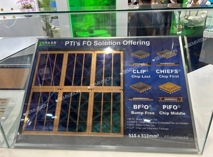
Large-Panel Development
PTI introduced an FOPLP solution with panel dimensions of510 × 515 mm, significantly larger than traditional wafers or smaller panels.
The larger form factor enables higher step efficiency and improved cost optimization, making it well-suited for scaling production.
Target Application Scope
PTI is not limiting its approach tolow-I/O or simple devices.
Instead, it is simultaneously addressing bothsmall I/O devicesandcomplex multi-chiplet integration.
Whetherheterogeneous(different chip types) orhomogeneous(same chip type), PTI is positioning FOPLP as a viable packaging solution for diverse integration needs.
Warpage Control
Warpage is one of the primary technical challenges in large-panel manufacturing.
PTI identifiedwarpage managementat the panel level as acore competency.
This involves:
Careful material selection
CTE (Coefficient of Thermal Expansion) matching
Process engineering around stress and thermal management
Integration with Optical Engines / High-I/O Demands
PTI introduced the idea ofoptical engine integrationduring the forum.
Given the broader context ofmulti-chiplet integrationandHPC/AI application demands, it is clear that PTI’s FOPLP roadmap is tightly linked with:
High-speed I/O requirements
Optical communication modules
Electro-optical heterogeneous integration
Such solutions demand:
High-densityRDL (Redistribution Layer)
Fineline/space dimensions
Strongsignal integrity and power controlwithin the package
Robust support forthermal managementandelectro-optical performance
ASE’s Commitment and the VIPack™ Platform
ASE is also making significant strides inFan-Out Panel Level Packaging (FOPLP), with itsVIPack™ platformserving as a showcase and benchmark for the company’s advancements in advanced packaging and system integration. Below are the key highlights of ASE’s strategy and technology positioning through VIPack:

VIPack Platform Structure and Scope
VIPack provides a comprehensive suite of advanced packaging technologies, covering multiple form factors, including:
Fan-Out Package-on-Package (FOPoP)with high-density RDL substrates
Fan-Out Chip-on-Substrate (FOCoS)
FOCoS-Bridge
Fan-Out System-in-Package (FOSiP)
2.5D/3D ICenabled byThrough-Silicon Via (TSV)
Co-Packaged Optics (CPO)capabilities for next-generation interconnects
This broad portfolio underscores ASE’s role as a leading integrator, capable of addressing diverse customer requirements acrossHPC, AI/ML, networking, and optical communications.

Technical Innovations and Differentiation
One of the most notable innovations in VIPack isdouble-sided RDL (Redistribution Layer)technology.
This approach increases interconnect density within the package and improves vertical (Z-direction) efficiency.
VIPack emphasizeshigh I/O density, large bandwidth, and robust power delivery, all of which are essential for advanced workloads such as AI training/inference, high-performance computing, and data-intensive networking systems.
Panel-Level Packaging Capability and Strategic Deployment
ASE already operates a310 × 310 mm panel-level FOPLP line in Kaohsiung, signaling that its panel-level capability has moved beyond the experimental phase into actual production.
Like PTI, ASE anticipates rising demand fromAI servers and data centers, wherehigh-throughput and massive I/O requirementswill drive panel-scale manufacturing.
This positions ASE to compete directly in scaling bothcapacityandyieldfor next-generation packaging.
Challenges and Bottlenecks (ASE + Industry-Wide Observations)
While ASE has built strong capabilities, the broader industry—including ASE—faces several critical hurdles in FOPLP:
Scaling Panel Size
Moving from300 mm to 500 mm panels or largerintroduces major stress management challenges.
Controllingmaterial stress, thermal stress, and warpageis central to manufacturability.
RDL Scaling
Shrinkingline/space dimensionsis necessary to support high-I/O, multi-chip systems.
This stresses lithography, metal deposition, etching, copper plating, and the reliability of interconnects such as copper lines, pillars, and solder joints.
Multi-Chiplet Integration
Electrical and signal integrity across multiple chiplets must be tightly controlled.
Power delivery and thermal managementinside the package are critical for stability and commercial viability.
Cost and Yield
If panel-level production cannot achieve yield and cost metrics close towafer-level packagingor other established approaches, adoption will slow.
High initial investment in equipment and material retooling is viewed as amajor barrierin industry reports.
ASE’s VIPack platform demonstrates the company’s ambition to offer a full-stack heterogeneous integration ecosystem, with innovations like double-sided RDL and panel-scale production lines already in place. However, the ability to balance scale, reliability, and cost efficiency will determine whether panel-level packaging becomes a mainstream commercial solution in the AI/HPC era.
The Relationship Between FOPLP and Optical Engines
AnOptical Enginetypically refers to a set of high-speed optoelectronic modules that integratelasers, modulators, photodetectors, waveguides, WDM multiplexers/demultiplexers,and electronic driver/receiver circuits. Integrating Optical Engines withFan-Out Panel Level Packaging (FOPLP)requires careful consideration of several technical dimensions:
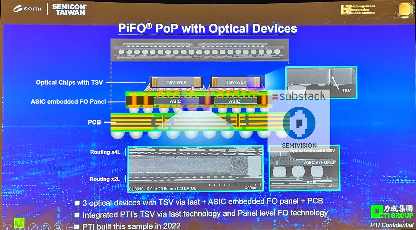
- Placement of Optical and Electronic Components
A central design question is whether optical and electronic devices areco-packaged within the same panel—alongside ICs, memory, and chiplets—or placed separately and connected viaoptical fibers or waveguides.
To support Optical Engines,panel-form FOPLPmust enable extremelyhigh-speed, low-loss RDL/interconnect layouts, while ensuringthermal, power, and signal integrity coordinationbetween optical and electronic devices.
- Signal Integrity and Electro-Optical Interference
Within large panels, electrical circuits and optical waveguides coexist, raising concerns about:
Thermal effects, EMI (electromagnetic interference), and crosstalk.
As RDL line width/spacing shrinks,RC parasitics increase, amplifying signal degradation risks.
Optical devices, being highly heat-sensitive, require carefully engineeredmaterials and structuresto mitigate interference and maintain performance.
- Thermal Management and Stability
Optical components—especiallylasers and modulators—generate heat during high-speed operation and are highly temperature-sensitive.
Panel-scale packaging makesthermal conduction and dissipationmore challenging.
Effective solutions must includeheat sinks, thermal interface materials (TIMs),and packaging materials with well-matched thermal conductivity and CTE.
- Packaging and Optical Coupling
Ensuringprecise alignmentof optical ports, fibers, and connectors within a large panel package is a major challenge.
Packaging must deliverhigh mechanical accuracy, vibration resistance, and environmental stability, all while maintaining cost efficiency and scalability.
- Process Compatibility and Design Tool Support
Photonic components (waveguides, modulators, detectors) must be supported inphotonic EDA toolswith design rules that align with FOPLP RDL and panel-level processes.
This requires collaboration acrossfoundries, OSATs, and packaging providers, offeringco-design supportfor both photonic and electronic integration.
To strengthen this ecosystem, OSATs such asPTImay need to providedesign kits, photonic IP blocks, and published RDL electrical/optical specsalongside reliability standards.
- Commercialization Milestones and Key Indicators
For FOPLP + Optical Engine integration to reach mass production, several milestones must be achieved:
Panel process maturity: reliable yields in panel size, RDL layer counts, and fine-pitch line/space metrics.
Pilot run success: validated integration of packaging with optical modules, demonstrating high-speed, long-distance, and multi-wavelength transmission.
Cost competitiveness: narrowing the gap with conventional electrical interconnects or wafer-level packaging.
Design wins: adoption of FOPLP + Optical Engine solutions byAI accelerators, HPC providers, and hyperscale data centers.

The integration of Optical Engines with FOPLP is not just a packaging innovation—it is astrategic enabler for next-generation AI and HPC infrastructure. Success hinges on achievingtechnical scalability (signal integrity, thermal, optical coupling), ecosystem alignment (EDA + foundry + OSAT), and commercial validation (design wins + cost competitiveness).
At this year’sFOPLP (Fan-Out Panel Level Packaging) Forum, the spotlight extended beyond OSATs and major packaging houses. What stood out was thegrowing importance of materials and inspection providersin shaping the next-generation packaging ecosystem. Several leading glass-core substrate and material suppliers—includingCorningandSHCOOT—were invited to share their perspectives on the role of glass in enablinglarge-panel FOPLPandhigh-density interconnects. With itslow dielectric constant, low signal loss, and a coefficient of thermal expansion (CTE) closely matched to silicon, glass is increasingly regarded as a promising successor to traditional ABF substrates. Its unique properties make it especially well-suited forhigh I/O, low-power applications, such as AI accelerators and HPC modules.
AGC: Applications for Glass-core substrate
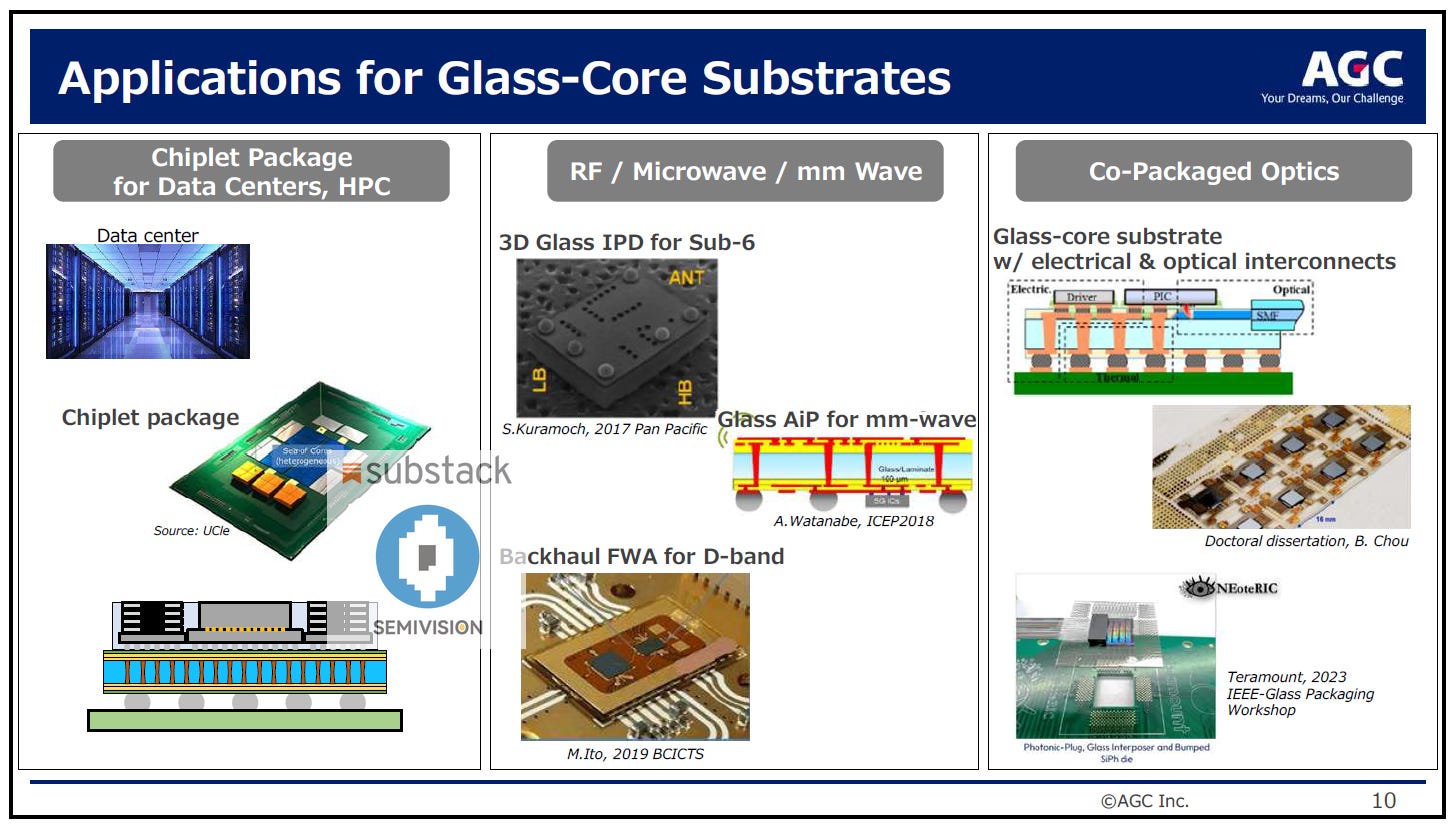
A notable point is that whileAGCdid not directly present at this forum, the company has articulated in other venues acomprehensive view on glass interposers and glass-core technologies. AGC has highlighted its technical strengths indimensional control, TGV (Through-Glass Via) reliability, and ultra-thin glass processing, reinforcing its position as a global key material supplier. At the same time,SHIKOjoined the discussion, contributing perspectives from diverse process and application domains. This broad participation underscored a critical shift: theglass material supply chain is no longer a supporting player. Instead, it has become adecisive factor in determining whether FOPLP technologies can achieve scalable mass production.
Senko: Expanded Beam , Detachable connectors for CPO

In the area ofinspection,COMETintroduced a3D X-ray solution, highlighting the shifting direction of advanced packaging inspection technologies. Traditional2D X-rayhas long been applied in advanced logic processes to detect defects and internal structures. However, with the rise ofmulti-layer heterogeneous integrationandlarge-panel FOPLP manufacturing, the complexity of structures and the need to identify finer defects make3D X-ray an essential tool. Through three-dimensional imaging, engineers can more accurately detectcracks caused by warpage,voids or poor metal filling inside TGVs, andminute misalignments or porosity in micro-bumps, thereby ensuring bothelectrical and mechanical reliabilityof the package.
COMET:3D X-ray solution for 3D Packing

Overall, this year’sFOPLP Forumhas clearly evolved beyond showcasing processes and platforms. It now extends into the two critical domains ofmaterialsandinspection, underscoring that the future of the advanced packaging ecosystem will rely onsynergistic collaboration among OSATs, material suppliers, and inspection solution providers. Only through such integration can FOPLP truly achievecommercial adoption in AI, HPC, and optoelectronic integration applications.
Heterogeneous Integration Tech Forum : Glass Core / Glass Substrate Supply Chain and Technical Perspectives
At this year’s FOPLP Forum, several key suppliers ofglass materialsandglass interposer/core technologies—includingCorning, SHCOOT, and AGC—were invited to share their perspectives. These companies’ investments in materials, manufacturing processes, and reliability are becoming essential enablers for the next wave ofFOPLP + Optical Integration + High-Concurrency / High-I/O Packaging.
AGC’s Glass Interposer and Glass Core Technology

3D X-Ray Inspection / Comet Yxlon’s CA20 System and Advanced Testing Needs
In advanced packaging and FOPLP applications, inspection technology is essential for ensuring yield, improving reliability, and accelerating mass production. At this forum, Comet Yxlon introduced its 3D X-Ray solutions. Below are the key features and applications of this technology.
Features and Applications of 3D X-Ray Solutions such as CA20
Non-destructive 3D inspection (3D computed laminography / computed tomography)
CA20 systems allow internal inspection without damaging the package or its structures. They can visualize bumps/micro-bumps, TSVs, copper pillars, and flip chips within highly integrated packages. This is critical for identifying interconnect defects in FOPLP or 3D packaging, such as voids, cracks, non-wetting, head-in-pillow, bump shift, and standoff height deviations.
High resolution and fine defect detection
The CA20 system achieves resolution below 1 µm, enabling the detection of extremely small defects like micro-cracks or voids, even near micro-solder joints and TSVs. Such details are often difficult to identify with traditional 2D X-Ray or optical inspection methods.
AI-driven automated interpretation and batch processing support
The system integrates AI-powered image analysis and automated reporting. Comet Yxlon’s CA20, paired with its CoS Insights software, can automatically detect typical defects and provide repeatable, production-ready inspection workflows. This accelerates R&D and production ramp-up, while reducing scrap rates caused by undetected defects.
Throughput and production line compatibility
Although high-resolution inspection is generally slower, systems like CA20 are designed with throughput, maintenance, and usability in mind. They are well-suited for advanced packaging production lines, serving in R&D, sampling, or in-process monitoring. Instead of scanning every die or panel in full 3D, selective or critical area scanning provides sufficient quality assurance without slowing down the entire production process.
Why 3D X-Ray Is Critical in FOPLP / Advanced Packaging Environments

Traditional 2D X-Ray or optical inspection faces significant limitations when dealing with multilayer interconnects or micro-scale joints (micro-bumps, TSVs, copper pillars). Occlusion and overlapping structures restrict viewing angles, making it impossible to detect hidden defects. In contrast,3D scanning or tomographic imaging (laminography / CT)enables inspection from multiple angles, helping to identify issues such assidewall voids in solder balls, misalignment, deformation of solder ball tops, or standoff/collapse problems.
Inpanel-level packaging, the large substrate size, thickness, and heterogeneous material stack (glass + organic materials + metals + adhesives) introduce thermal stress and mismatches in material expansion/contraction. These can causewarpage, internal stress, micro-cracks, or adhesion failuresduring processing. 3D X-Ray is vital for detecting such defects early, enabling corrective action before yield is impacted.
Foroptoelectronic integration(optical engines, waveguides, optical connectors) andmulti-chip integration (chiplets), the demands for signal integrity and power integrity are extremely high. Even minor defects — such as solder joint failure, wire discontinuity, or voids — can degrade bandwidth, introduce signal loss, and ultimately compromise module performance and reliability.
Inspection technology directly impactsyield and cost control. Early defect identification canreduce scrap, accelerate yield ramp-up, and cut down the time and cost required for testing and rework.

Corning’s Strategy in Glass Materials and Applications in Glass Substrate / Glass Core

As a long-established giant in the field ofglass materials(glass substrates, glass carriers, glass cores, and glass interposers),Corninghas been gradually clarifying its strategy and technology roadmap for advanced packaging and FOPLP applications. Below are its key technologies and market applications:
Core Technologies and Product Capabilities
Fusion Forming Process Platform
Corning has its proprietaryfusion forming processtechnology platform, capable of producing glass panels withpristine surface qualityand high strength. These glass panels are used as substrates, carriers, or glass cores. Their superior surface smoothness reduces defects during processing and improves overall stability in packaging.
Through-Glass Via (TGV) and Support for Glass Interposers / Cores
In recent presentations, Corning highlighted applications of glass cores and interposers usingTGV (Through-Glass Vias)to enable vertical, double-sided, or multi-layer electrical connections. This allows glass to serve not only as a substrate or carrier but also as a functional interposer, supportinghigh-density and high I/O packaging designs.
Variety of Glass Types and Performance Characteristics
Corning offers a diverse portfolio of glass compositions, featuring different optical properties, mechanical strength, thermo-mechanical stability, thermal conductivity, and compatibility with conventional packaging materials (e.g., RDL, metal interconnects, adhesives). This broad range enables designers to fine-tune material selection to meet specific performance requirements.
Control of Warpage and Reliability
A key challenge for glass materials is warpage, dimensional stability, and coefficient of thermal expansion (CTE) matching. Corning addresses this throughmaterial combinations(e.g., fused glass, laminated glass),thickness control, and optimizedprocess handling. For example, itsglass carrier solutionscan reduce warpage during processing by up to40% compared with traditional methods.
Glass Adaptive / Die-Embedded Structures
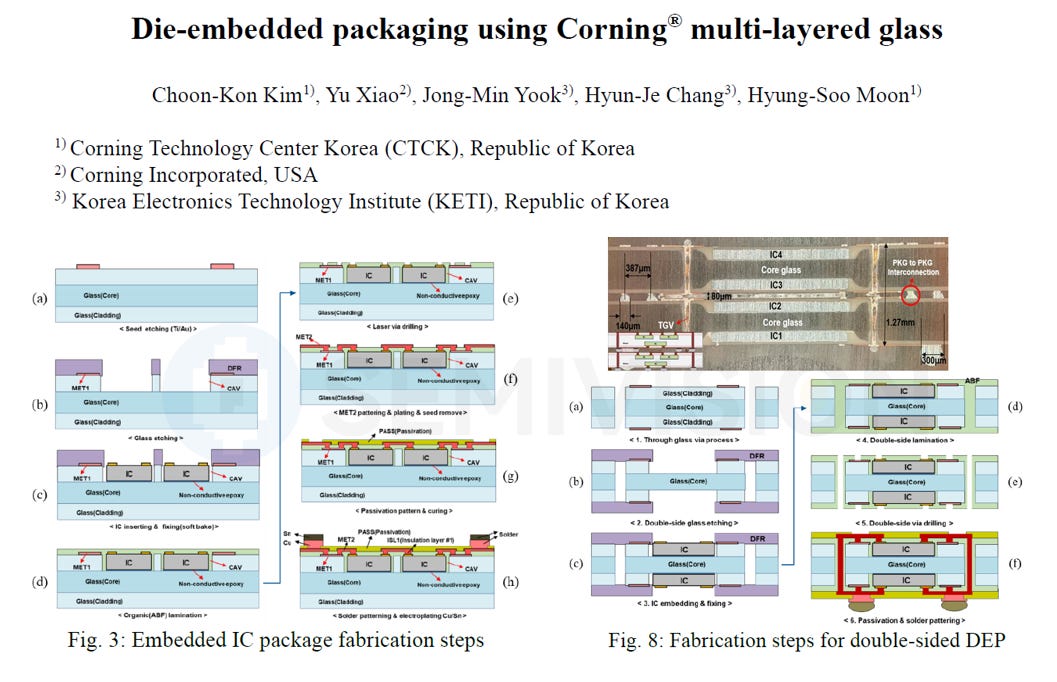
Corning’sAFG (Adaptive Formed Glass)technology exemplifies this approach. Research prototypes have demonstrateddie-embedded packageswhere chips are embedded into cavities within glass substrates, supported by TGV for single- or double-sided interconnects. This design enables glass to take onmore complex interconnect roles, not just as a passive carrier.
Glass Carriers for Temporary Support in Advanced Packaging
Corning also supplies glass for use astemporary carriers, particularly inwafer thinningortemporary bondingprocesses. While these are not final functional substrates, they play a crucial role in advanced packaging flows, especially for high I/O density and wafer-level processing.
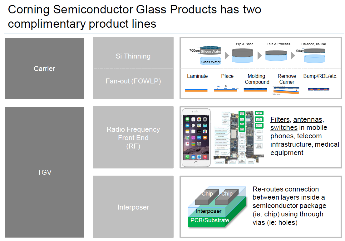
How Glass Substrate / Glass Core Are Applied (Integration with FOPLP / Advanced Packaging)
Based on Corning’s technology and market roadmap, here is how they apply their innovations toglass substrates/coresand the roles they play inFOPLP and panel-level packaging:
Application Areas
Panel-level Packaging
Corning’s solution / advantage: Using glass as the panel substrate/core or as an interposer improves dimensional stability and surface flatness, enabling high-density interconnects and large-panel packaging. Corning highlights its superior surface quality and mechanical strength for such applications.
Applicable scenarios / challenges: Large panels (e.g., 510×515 mm) face issues such as warpage, polishing/processing difficulty, and higher risks in cutting and handling. This requires glass with a balanced design of thickness and strength.
Interposer / Through-Glass Via (TGV) Support
Corning’s solution / advantage: TGV technology enables vertical or double-sided electrical connections, allowing the required interconnectivity and routing density for interposers to be realized on glass instead of organic or metal substrates. Corning emphasizes the reliability of its glass and metallization processes.
Applicable scenarios / challenges: Challenges include uniformity of via filling, adhesion at the glass–metal interface, thermal cycling endurance (especially during solder reflow and molding), and the impact of vias on electrical/signal integrity.
Die-Embedded Packaging
Corning’s solution / advantage: Corning’s AFG has demonstrated support for single- or double-sided die embedding, as well as package-on-package structures. Compared with traditional packaging, this offers advantages in thickness and interconnect density. Precision cavity fabrication (e.g., differential etch rates), bottom surface planarity, and dimensional control ensure proper alignment and flatness when chips are placed in cavities.
Applicable scenarios / challenges: Scaling such embedded packaging to panel-level mass production faces cost, process time, and yield challenges. Critical issues include sidewall angle control of cavities, die placement accuracy, electrical consistency between packages, and CTE matching of all materials.
Warpage and Reliability Control
Corning’s solution / advantage: Corning provides warp-reduction solutions such as glass carriers, along with fusion forming and laminated glass technologies, to control deformation under thermal and mechanical stress. This is especially important for FOPLP processes involving large panels, many process steps, and high thermal/mechanical variability.
Applicable scenarios / challenges: Panel fabrication and packaging must account for thermal shocks, mechanical handling, stresses from adhesives/resins, as well as humidity and contamination. While glass is dimensionally stable, risks of cracking or fractures remain.
Integration with Other Packaging Technologies / Materials
Corning’s solution / advantage: Corning envisions hybrid structures combiningglass substrates + TGV + die embedding + RDL + organic polymer interconnects. The goal is not merely to sell glass but to provideglass core solutionsfully integrated into panel-level packaging flows.
Applicable scenarios / challenges: Design and process integration must simultaneously address electrical interconnects, thermal management, reliability (lifetime, thermal cycling, humidity resistance), and material compatibility. Design tools and standards must also evolve to support glass-specific requirements such as via design and surface flatness.
Market and Technical Barriers / Open Issues
While Corning’s glass material roadmap provides significant advantages, several challenges remain for full deployment in FOPLP, optoelectronics integration, and large panel-level packaging:
Handling of thin glass / optimizing strength and toughness: Thinned glass is fragile and prone to breakage under mechanical stress or handling.
TGV filling / metallization uniformity: Reliability of via fill (avoiding voids), adhesion of metal to glass, and the impact of vias on impedance and signal loss.
CTE mismatch between glass and other packaging materials: Differences with resins, adhesives, and metals can introduce stress during soldering, molding, or environmental cycling, affecting reliability.
Cost and mass-production capability: Glass material and processing (cutting, sawing, handling, finishing) are more expensive at large panel sizes. Scaling up requires a mature supply chain, equipment, and processes to reduce costs.
Design standards and reliability data: Compared to long-established ABF or FR-4 substrates, glass substrates still lack extensive reliability data for long-term thermal cycling, humidity, and mechanical stress. Customer confidence and standardized benchmarks are still in development.
Semiconductor Supply Chain Driving Next-Generation Advanced Packaging (KINK &PSI)
With the growing demand for performance and energy efficiency from AI, HPC, and data centers, the semiconductor industry is entering a new competitive era centered onadvanced packaging. This transformation relies not only on breakthroughs in wafer manufacturing, but also on thecoordinated deployment of the entire supply chain— spanning materials, equipment, and inspection.
- Materials Localization: Strengthening the Supply Chain Foundation
KINK: By controlling over70% of the global market sharein CMP diamond discs, KINK serves as a critical consumables supplier for advanced CMP processes at TSMC, Samsung, and Intel. It plays an irreplaceable role at the 3nm and even 2nm nodes.Website
PSI: Specializing inreclaimed wafers and carrier wafers, PSI provides indispensable substrates for wafer handling, thinning, and testing in packaging processes. As panel-level packaging and large wafer formats gain traction, localized supply of reclaimed wafers has become crucial forcost control and capacity assurance.

CMP and Wet Process Equipment:
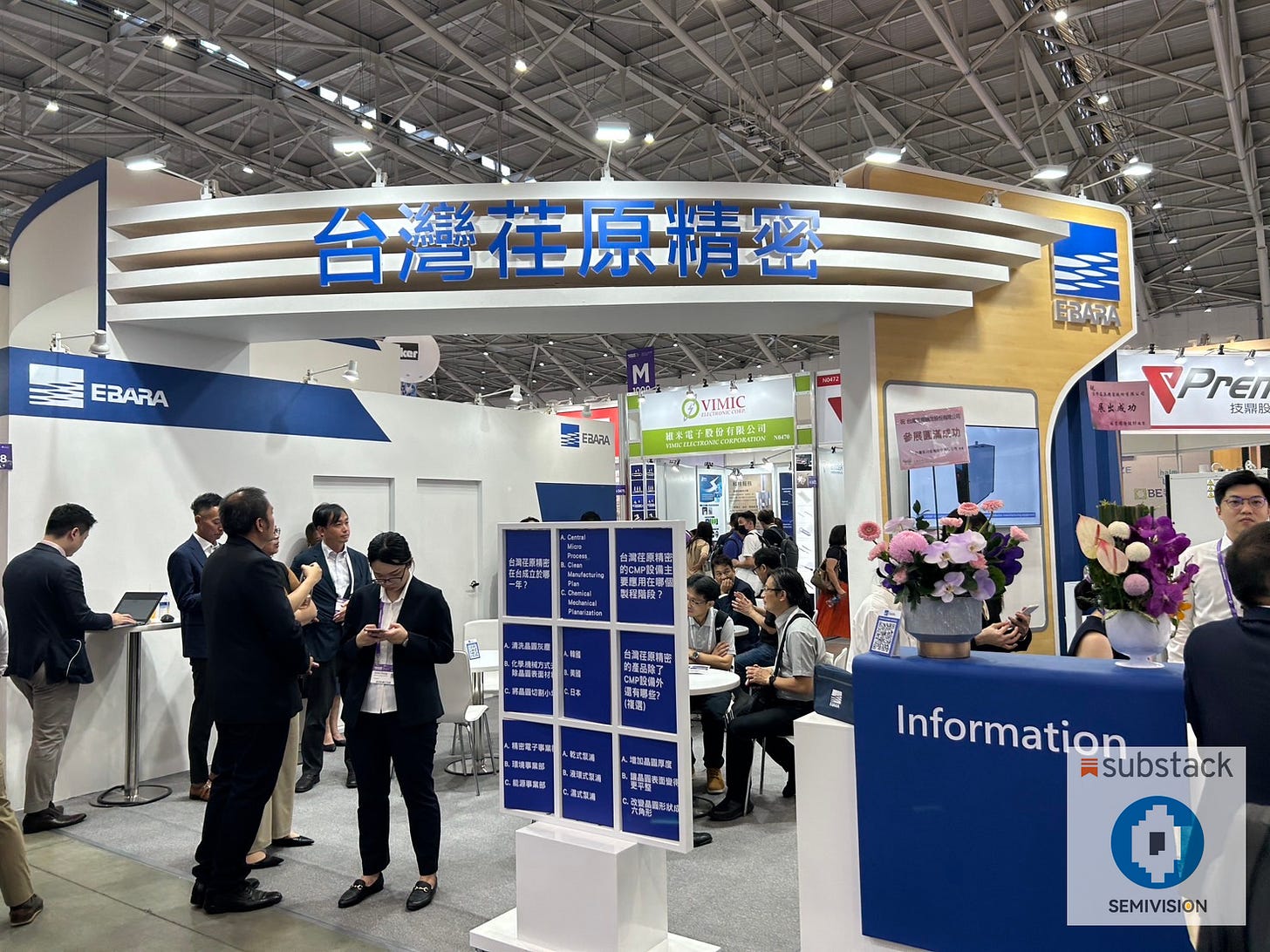
Ebarais a key supplier, offering CMP polishers, ECP/ECD plating systems, cleaning equipment, and vacuum dry pumps, enabling comprehensive process solutions.Website
Applied Materials (AMAT)supports advanced packaging with its Reflexion CMP series, plating systems, and cutting-edge PVD/CVD/ALD thin-film equipment, essential for multilayer RDL and high-density interconnects.
Consumables: The consumables supply chain includes polishing slurries, pads, and diamond conditioners, provided by global and local material suppliers such asEntegris/Cabot, DuPont, AGC, andKINK(diamond conditioners). Achievinglocal mass production of critical consumables and selected equipmentis at the heart of the “Local-to-Local” policy.
Process Equipment: Extending Front-End to Back-End (LAM & TEL & SCREEN )
Lam ResearchandTEL (Tokyo Electron)are representative cases of front-end technologies being transferred into packaging. Lam’sALD/etch platformsare now applied to RDL and TSV processes, ensuring consistency between barrier layers and metals to prevent high-frequency signal loss. TEL, meanwhile, emphasizesone-stop deposition, etch, and cleaning solutionswith a focus on production automation.

SCREEN Holdingsspecializes inpanel-level cleaning, providing uniform surface treatment for large FOPLP substrates (>500 mm × 500 mm). Its solutions address challenges such as particle contamination and interface residues.
Together, these companies form a bridge betweenwafer front-end and packaging back-end, ensuring the reliability ofheterogeneous integration (HI).
Bonding and Packaging: The Core Driver of Interconnect (EVG & BESI & ASMPT & HANMI & K&S)
In bonding and stacking,EVG (EV Group)is the leader in bothwafer-to-wafer (W2W)anddie-to-wafer (D2W) hybrid bonding.
EVG offersCollective D2WandDirect Placement D2Wprocesses, targeting high-throughput and high-precision applications respectively.
A joint demonstration withCEA-Letishowed that EVG has achieved1 μm pitch Cu/oxide hybrid bonding on 300 mm wafers, with overlay accuracy of less than 200 nm (3σ), setting a technical benchmark for chiplet and 3D IC commercialization.
EVG’sHICC (Heterogeneous Integration Competence Center)supports customers in testing and process incubation before full adoption of hybrid/fusion bonding, helping accelerate volume production.
BESIandASMPTare emerging as two powerhouses in Europe and Asia, aggressively expanding hybrid bonding capacity:
BESI reported in Q2 2025 that hybrid bonding orders have risen sharply, driven byHBM4 and advanced logicdemand.
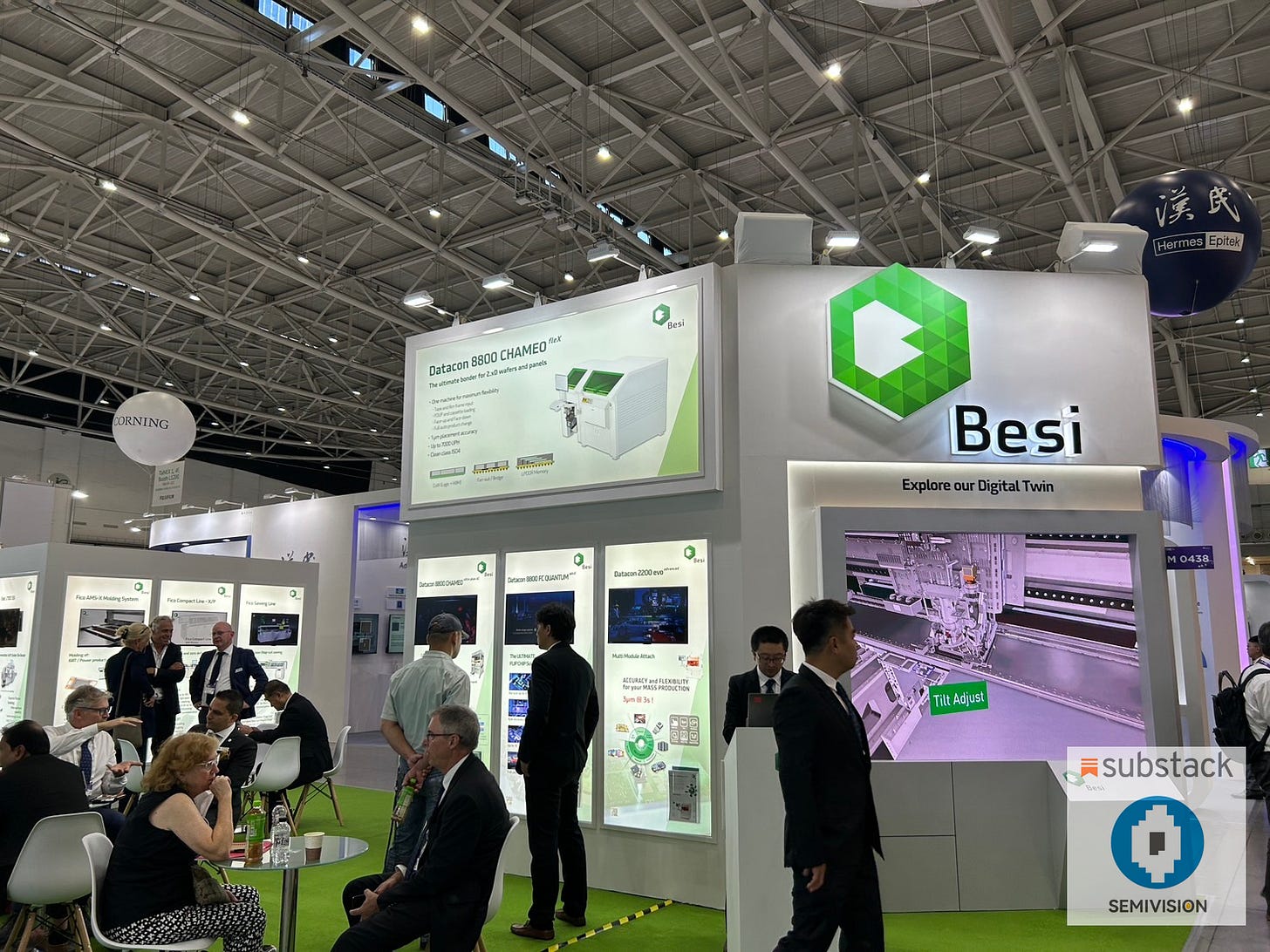
ASMPT has secured multiple hybrid bonding orders from IDMs and foundries, with deliveries scheduled in the second half of 2025.

Applied Materials’ acquisition of a 9% stake in BESIsymbolizes a strategic integration of equipment and front-end materials, positioning hybrid bonding as acritical bridge between front-end and back-end technologies.
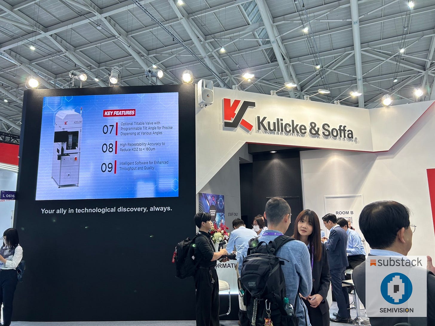
Hanmi SemiconductorandK&Sare focused onfluxless TCB (Thermo-Compression Bonding)andHBM:
Hanmi invested100 billion Korean dollarto launch a commercial hybrid bonder by 2027, and released theTC Bonder 4, designed specifically for HBM4 alignment precision and stacking efficiency.
Hanmi, in collaboration withTES, is strengthening front-end pre-treatment (thin-film deposition and surface treatment) to addressHBM 16-Hi challenges.

K&S is focusing on fluxless TCB, emphasizing oxidation control and low-temperature bonding. It has already been validated in certainCoWoS-Lprocesses.
TOWAcontinues to optimizecompression molding, reducing warpage and void rates, which is especially critical foroptoelectronic modules (CPO/OIO)and large-format packaging.
Industry Trend: Starting withHBM4, the market is generally adopting a“dual-track strategy”— running traditional TCB and hybrid bonding in parallel — to ensure optimal trade-offs across cost, performance, and yield for different application scenarios.

2025年7月11日
Metrology and Inspection: Guardians of Yield (ONTO & DISCO &Lasertec)
Onto Innovationhas introduced subsurface defect inspection into packaging lines, providing in-line solutions for bonding interface cracks and voids, gradually becoming a guarantor of yield for HBM and chiplet packaging.

Discoremains the leader in wafer thinning and panel-level dicing, offering blade and laser-based solutions that ensure cutting precision for large-area FOPLP, preventing edge chipping and micro-cracks.Discohas launched theDFD6370 dicing system, capable of supporting large panels up to330 × 330 mm, bringing a significant impact on FOPLP production capacity and cost structure. Meanwhile,Veeco, leveraging itsAP300™ lithography platformand wet process tools, has secured major orders fromIDMs and OSATs, establishing a solid position inhigh-density fan-out and optoelectronic integration applications.

Lasertechas extended its EUV mask inspection expertise into packaging RDL, delivering high-resolution defect detection for1–2 μm line widths, providing critical support for RDL scaling.

Veecohas secured new orders for its packaging lithography and ALD platforms, supporting fan-out and Cu-pillar processes. However, in the ALD market,AMATandASMremain the dominant suppliers; Veeco’s advantage lies in customized, flexible solutions tailored to packaging.
From thelocalization of materials and consumables, to thecross-boundary extension of equipment and processes; frombreakthroughs in bonding and interconnects, tometrology and inspection safeguarding yields— the semiconductor supply chain is now driving next-generation advanced packaging with unprecedented cohesion.
The demands ofAI and HPCare transforming chips from standalone logic devices intomulti-chip stacks, optoelectronic integration, and system-level packagesthat require deep collaboration across the ecosystem.
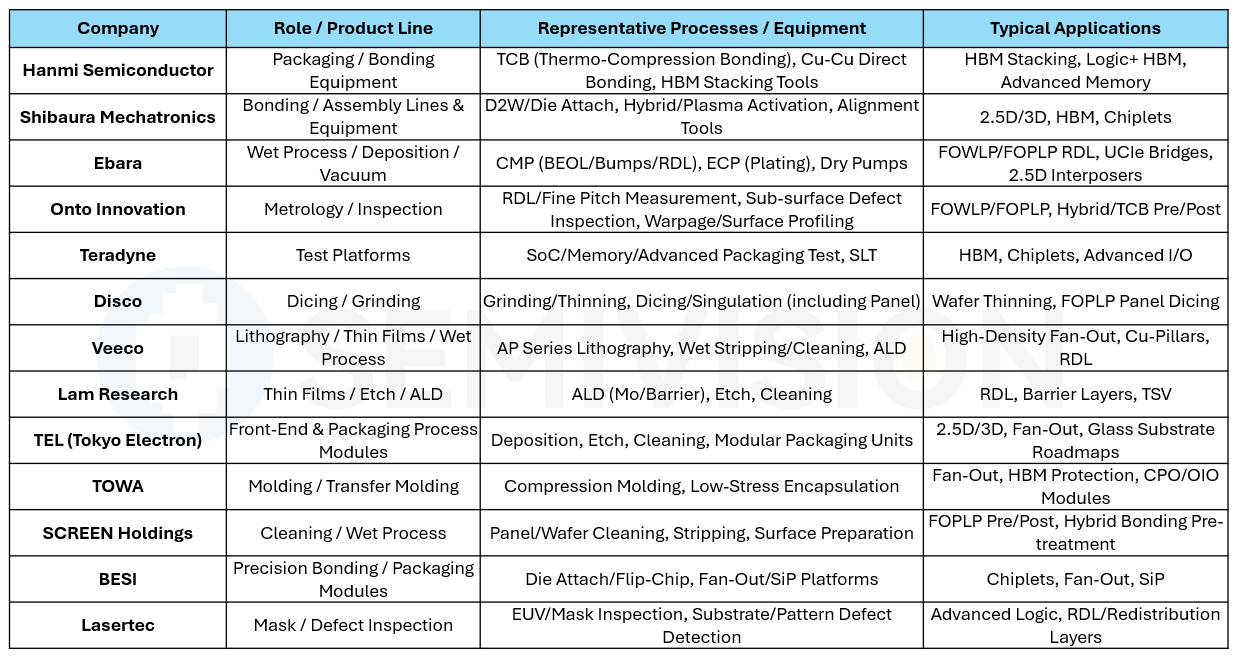
Companies includingEVG, BESI, Hanmi, ASMPT, K&S, KINK, PSI, Ebara, Lam, TEL, SCREEN, TOWA, Onto Innovation, Disco, Veeco, and Lasertecare together building this new ecosystem.
In the future, whoever captures thetechnological high ground along this complete value chainwill emerge as the key winner in thepost-Moore’s Law era.
Company Updates / SEMICON Taiwan Highlights (SUSS MicroTec & Advantest & TEL)
SUSS MicroTec
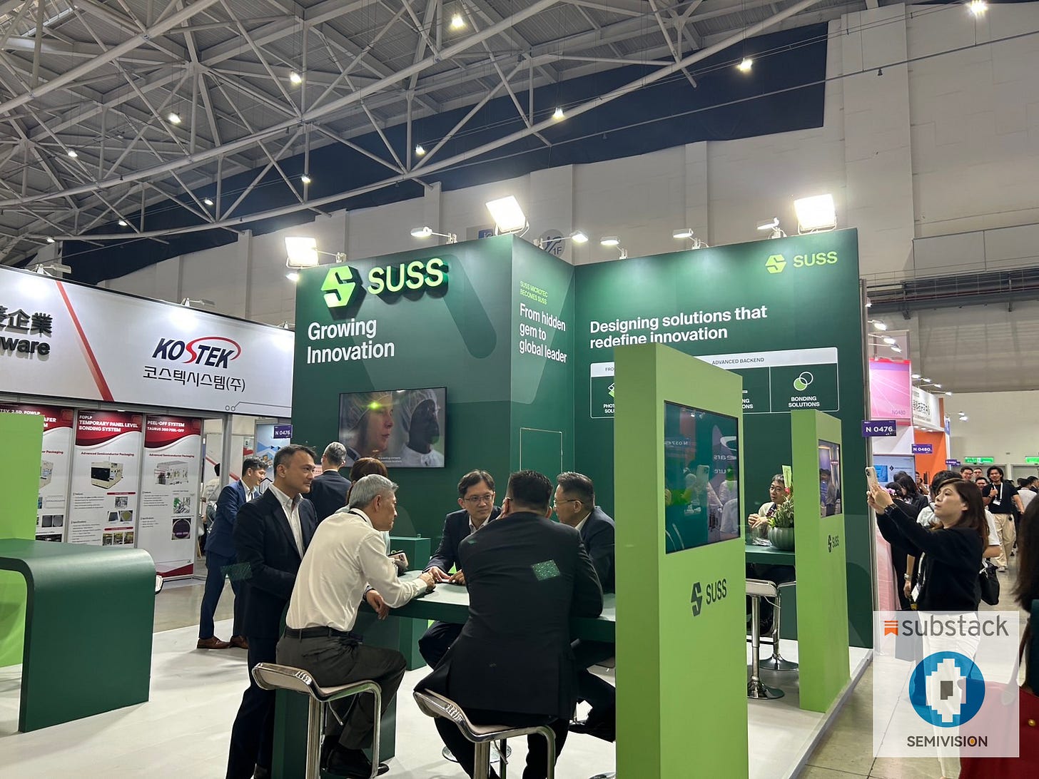
At SEMICON Taiwan, SUSS MicroTec showcased its latest solutions inhybrid bonding, advanced packaging, and 3DIC. On the tools and technology front, they introduced the newDie-to-Wafer (D2W) hybrid bonding system, XBC300 Gen2, an integrated machine that combines surface activation, alignment, and bonding. It is designed for high accuracy and stringent overlay requirements.
Advantest
At SEMICON Taiwan 2025, Advantest announced it would present“innovative, sustainable test technology”, aligning with its new corporate vision:“Be the most trusted and valued test solution company in the semiconductor value chain.”Its Taiwan subsidiary also celebrated its 30th anniversary. On the business side, due to rising AI-driven test demand, Advantest has raised its full-year operating profit forecast.

Tokyo Electron (TEL)
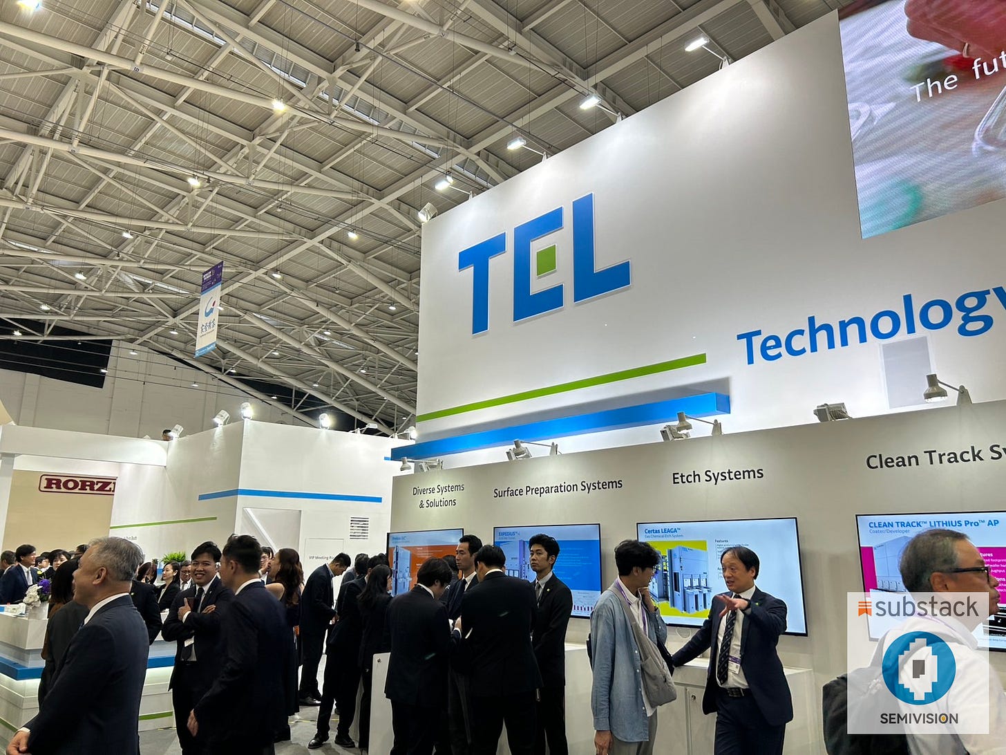
TEL was one of the platinum sponsors of SEMICON Taiwan 2025. Executives such as Corporate Officer Hiroshi Ishida delivered talks at theSemiconductor Sustainability Summitand theIC Forum, covering themes such as process efficiency, digital transformation, and sustainable manufacturing. TEL was also recognized during the forum as one of Japan’s most active equipment makers inadvanced packaging and heterogeneous integration.
Materials / Supply Chain & Overall Exhibition Trends
At theStrategic Materials Conferenceduring SEMICON Taiwan 2025, discussions focused heavily onmaterials R&D, including dielectric materials, epitaxial materials, hybrid bonding materials, and thermal interface materials. This underscores the growing importance of material suppliers, particularly in the upstream and downstream of advanced packaging and integration.
Overall, the exhibition highlightedadvanced packaging— includingFOPLP, 3DIC, and heterogeneous integration— as a key enabler for the next stage of scaling mass production and achieving system-level integration.
Local Supply Chains Driving the Infrastructure for Advanced Packaging (G2C+ & KINK )
As process nodes continue to shrink and advanced packaging rapidly expands, the semiconductor industry’s reliance onconsumables, reclaimed wafers, and front-end processing equipmentis deepening. These elements, often seen as back-end support, have in fact become thefoundation influencing yield, cost, and capacity expansion.
In theCMP consumablesfield,KINKcommands nearly70% global market sharein diamond disc products, providing indispensable planarization capability for 3nm and next-generation nodes. With the rise of multilayer structures and complex interconnects, the number of CMP steps is increasing, making the quality and supply stability of consumables the lifeline of the process.
Forreclaimed wafers and carrier wafers, companies likePSI, KINK, and Scientechare continuously expanding capacity. These wafers serve as the foundation for wafer thinning, packaging support, testing, and yield verification. Demand is surging particularly inFOPLP and advanced logic processes.Shengyang’s reclaimed wafer business already accounts for more than 80% of its revenue, underscoring its heavyweight position in the global supply chain.
In the field ofwet etching, cleaning, and pre-treatment, both Taiwanese and international suppliers provide cleaning solutions, etchants, and adhesion tools to support interface activation and bonding-related yield control. Initiatives like theG2C+ alliance, which combines multiple equipment vendors to promote local AOI, polishing, and surface treatment solutions, are becoming the front line of Taiwan’s“Local-to-Local” strategy.

Though often considered auxiliary, these supply chain segments form thecritical infrastructure of advanced process and advanced packaging. With the support of diamond discs, reclaimed wafers, and wet etching/cleaning tools, the industry can continue pushing chip performance to new heights under the demands ofAI and HPC.
A New Chapter in Advanced Packaging for the Chiplet Era
As Moore’s Law slows, thechiplet architecturehas become an industry consensus. From AMD’s pioneering adoption of chiplets in commercial CPUs to the modular design strategies now pursued by major chipmakers, semiconductors are entering a new era of integration.
This shift is driving the adoption of advanced packaging technologies such asSoIC (System on Integrated Chips), which can be categorized intoWafer-on-Wafer (WoW)andDie-to-Wafer (D2W)approaches. However, to enable chiplets to scale into mass applications, traditionalTCB (Thermo-Compression Bonding)alone is no longer sufficient. Instead,Hybrid BondingandFluxless TCBare emerging as the next-generation interconnect technologies.
EVG and Hybrid Bonding Leadership
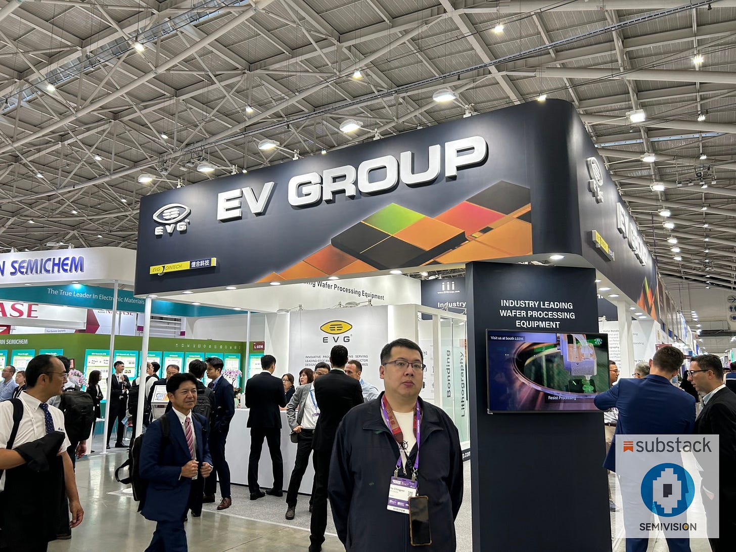
In theHybrid Bonding / Wafer-to-Wafer (W2W)space,EVG (EV Group)is a leading force:
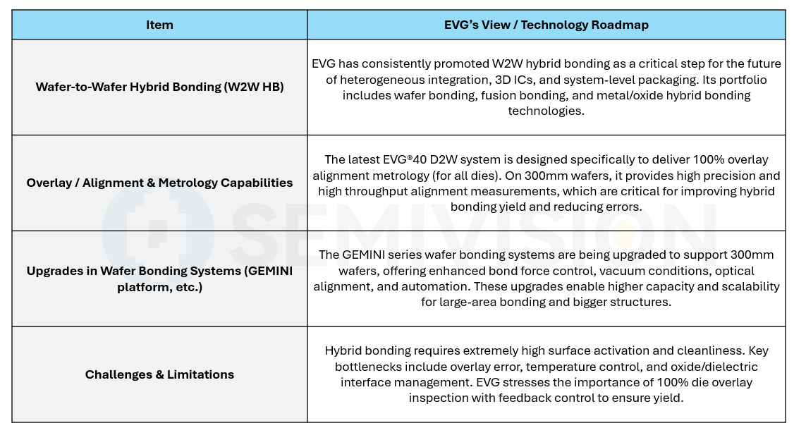
EVG has long emphasizedW2W hybrid bondingas the core path for heterogeneous integration and 3D IC, establishing leadership with bothfusion bondingandmetal/oxide hybrid bondingtechnologies.
TheEVG®40 D2W systemis designed specifically for100% overlay alignment measurement, providing high-precision, high-throughput full-wafer inspection on 300mm wafers—critical for yield and error correction.
Fluxless TCB and D2W Hybrid Bonding Expansion
Alongside hybrid bonding,fluxless TCB and D2W hybrid bondingare also evolving rapidly:
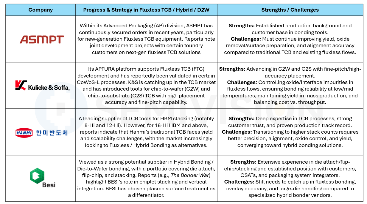
ASMPTis co-developing fluxless TCB with multiple foundry customers, with applications extending toHBM stackingthrough hybrid bonding.
K&S’sAPTURA platformsupports fluxless TCB and has already been validated inCoWoS-Lprocesses, though oxidation control and throughput remain challenges.
Hanmi Semiconductorhas built a strong position in HBM stacking with itsTC Bonder series, achieving stable results in8-Hi / 12-Hi stacks. However, for16-Hi and above, the market increasingly sees fluxless/hybrid bonding as essential.
BESIhas established strengths indie attach, hybrid bonding, and multi-die stacking, withplasma surface treatmentas a differentiator, positioning itself as a key player in chiplet stacking and heterogeneous integration.

2025年7月13日
Market Outlook: Dual-Track Competition
Overall, the next wave of advanced packaging is centered onchiplets, withhybrid bonding and fluxless TCBforming the foundation for making chiplet architectures truly viable. The market is moving toward adual-track competitive landscape:
W2W / Hybrid Bonding: Focused on achieving finer pitch and higher yield, ideal forhigh-performance computing, heterogeneous integration, and HPC applications.
Fluxless TCB: Prioritizing throughput and yield optimization, well-suited forHBM and other high-layer memory stacks.
As EVG emphasizes with its100% die overlay inspectionandfull-wafer metrology,yield management, surface activation, and interface puritywill be the decisive thresholds for scaling chiplet and SoIC technologies into mass production.
Trends in Hybrid Bonding / W2W and EVG’s Perspective
EVG (EV Group)is a major player in this field. RegardingHybrid Bonding, particularlywafer-to-wafer (W2W)applications for the next generation, EVG has outlined the following views and technology roadmap:
As the semiconductor industry transitions into thechiplet and HBM era, bonding technologies such asFluxless TCB, Hybrid Bonding, and Die-to-Wafer (D2W)are becoming critical enablers for high-yield, fine-pitch interconnects. Leading equipment suppliers are positioning themselves with distinct strategies, strengths, and challenges in this evolving landscape.
The following table provides a comparative overview ofASMPT, K&S, Hanmi Semiconductor, and BESI, highlighting their progress, competitive advantages, and areas where further breakthroughs are needed.
Core Technical Challenges & Future Watch Points
From the strategies of these companies, severalcommon technical challengesandfuture areas to monitorcan be identified:
Overlay / Alignment / Placement Accuracy
Ashybrid bonding pitch shrinksand die sizes/functions become more diverse, the tolerance for alignment error is decreasing.
For D2W or W2W hybrid bonding to achieve high yield, companies likeEVGemphasize the need for100% die overlay measurement and full-wafer inspectioncapabilities.
Fluxless Technology & Interface Oxide Management
Traditional TCB often uses flux or other means to remove/control oxidation and adhesion at interfaces.
Fluxless TCB(e.g., using formic acid vapor, plasma activation) aims to achieve the same or better interface purity and connectivity without flux. Companies likeK&S, ASMPT, and Hanwhaare actively investing in this area.
Stack Height Expansion
AsHBM moves to 16-Hi and beyond, challenges withthermal expansion, stress, thickness, and warpage managementbecome more severe.
Hybrid or fluxless bonding is viewed as one of the main solutions to address these issues.
Tool Throughput & Integration of Metrology / Inspection
In high-volume manufacturing, it’s not enough for tools to perform hybrid bonding or TCB — they must also deliver sufficientthroughput.
Supporting inspection and metrology systems (overlay measurement, in-situ error correction) must be fully integrated to keep pace.
Material Surface Treatment & Cleanliness
Factors such assurface roughness, oxide layers, and interface contamination(particles, organic residues) critically affect bond quality.
In fluxless or hybrid bonding flows, these aspects are particularly decisive.
Cost vs. Yield vs. Maturity Trade-Off
While hybrid bonding and fluxless bonding offer technical advantages (thinner stacks, lower signal loss, better performance), they involvehigher costs, longer R&D and process qualification cycles, and initially unstable yields.
Many companies are still in thecustomer validation or early adoptionphase, working toward establishing mature, reliable processes.
Henkel’s Material Strategy and Advanced Packaging Reliability for AI Chips
As AI chips continue to push towardhigher power consumption, greater compute density, and finer-pitch interconnects,advanced packaging reliabilityhas become a critical threshold for overall system performance. In the past, chip design revolved around logic and process technology; today, underchiplet, HBM, and heterogeneous integration architectures,material choices and packaging detailsdirectly determine the stability and lifetime of AI chips.
Henkel’s advanced packaging material portfolio is tailored to meet these demands:
LCM Overmold and Liquid Molded Underfill: Provide low warpage and excellent gap filling, ensuring large modules maintain mechanical stability during long-term operation.
Die Attach Film (DAF) and Non-Conductive Film (NCF): Control bonding thickness and transparency, enabling high I/O density chiplet interconnects while reducing thermal stress.
Capillary Underfill: Offers fast flow and thermal stability, protecting fine-pitch solder joints from failures caused by thermal cycling during high-speed computation.
Thermal Interface Materials (TIMs) and Lid/Stiffener Attach: Deliver low thermal resistance pathways to dissipate the high heat flux of AI chips, while minimizing package deformation.
These materials are not merely passive protection layers — they areactive enablers of long-term chip stability, allowing AI devices to operate reliably under high current loads and extreme temperatures.
In the future, the competitiveness of AI chips will hinge not only on compute performance, but also onwho can build a complete solution chain that links packaging materials, thermal management, and structural reliability.

Inspection and Testing: The Quality Safeguard of Advanced Packaging
In the rapid evolution of advanced packaging,inspection and testingare no longer auxiliary back-end steps — they have become thecore safeguard of yield and reliability. Aschiplets, SoIC, hybrid bonding, and HBM stackingmove into mass production, every hidden defect, every alignment error, and every potential crack from thermal cycling represents a critical risk to the stable operation of AI and HPC chips.
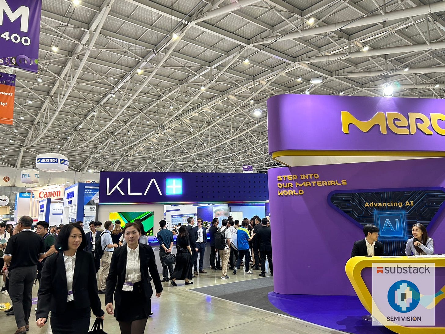
Today, the global inspection landscape is led byKLA, ONTO, Camtek, C-MET, and Nova, each providing solutions in defect detection, subsurface crack analysis, AOI, and optical metrology. These tools go beyond surface defect inspection — they penetrate intowafer thinning processes and hybrid bonding interfaces, holding the line on yield.
In testing,Advantest and Teradynedominate with advancedAutomatic Test Equipment (ATE) platforms, supporting requirements forhigh-speed SerDes, optical interconnects, and high-layer HBM stack testing. Their role is not only to verify whether a chip “functions,” but also whether it canoperate reliably under prolonged, high-frequency workloadswithout failure.
2025年8月10日
This underscores a shift: inspection and testing are evolving from traditional quality checks into theguardians of advanced packaging reliability— forming the foundation for next-generation AI chips to achievehigh performance, low power, and long lifetimes.
Inspection & Testing Supplier Landscape and Trends
Under the trend ofhigh-density interconnects and heterogeneous integrationin advanced packaging,inspection (inspection + metrology + process control)andtesting (final test / ATE)have become critical to ensuring yield and reliability. Below are key suppliers and observations on their positioning:
KLAhas established itself as a leader in advanced packaging process control, offering inspection and metrology tools for wafers, panels, and components. Its updated “IC Substrate Product Portfolio” highlights solutions for the growing demands of high-density interconnects in IC substrates and interposers. With platforms such asDirect Imaging (DI)and integrated defect inspection + metrology + chemistry process control, KLA addresses crucial packaging steps includingRDL, Cu pillars/bumps, TSVs, post-dicing, and pre-bonding. Systems like theKronos™ 1190can detect extremely fine defects — down to ~150nm — which significantly improves yield. This capability ensures the integrity of interconnects and substrates inchiplet and SoIC architectures, reducing risks of signal distortion or thermal failures, which are essential for the reliability of AI and HPC devices.
ONTO Innovationhas not made major recent announcements specific to advanced packaging at SEMICON Taiwan, but it already holds a solid portfolio in wafer thinning, RDL, and packaging inspection/metrology. Its potential to deliverin-line, high-throughput, high-precision detectionof subsurface cracks, bonding voids, and alignment deviations would be a critical enabler forchiplet integration and hybrid bonding yield improvement.
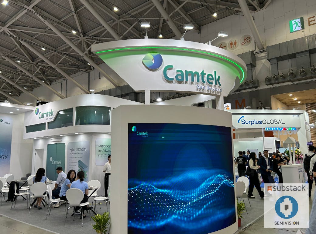
Camtek, C-MET, and Novahave less public visibility, but they are active in providingX-ray inspection, 3D hidden structure inspection, and AOI/visual inspection toolsto certain customers or regions. While their market exposure may be lower than KLA or ONTO, the growing complexity of advanced packaging is raising the importance of these tools. Early detection ofwarpage, voids, microcracks, and alignment errorsis vital to minimizing downstream yield losses and reliability failures.
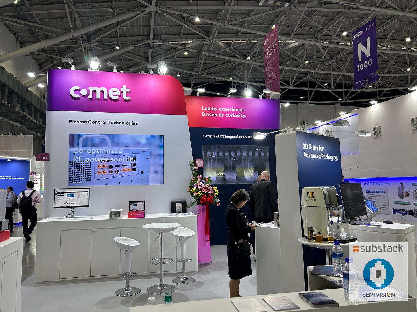
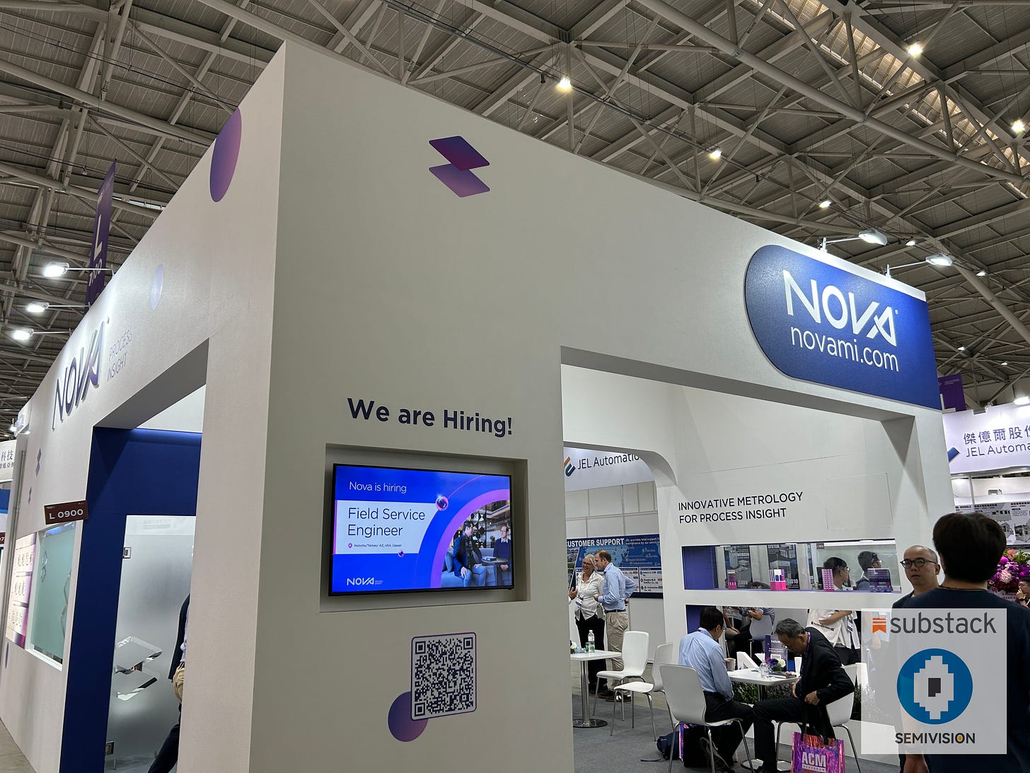
In short, inspection and metrology are no longer back-end safeguards but central to enablingscalable, reliable advanced packagingfor the chiplet and AI era.
In the testing domain, Advantest continues to hold a strong leadership position in Assembly Test Equipment (ATE). At SEMICON and other industry events, the company showcased its latest testing solutions, which have been enhanced for AI, high-speed interconnects, and optical/SerDes applications. Advantest also ranked highly in customer satisfaction surveys, reflecting that service and delivery capability are critical differentiators in the test market. Its technologies and platforms must support ultra-fine pitch, ultra-high-speed SerDes and optical I/O, as well as testing for advanced high-stack devices. However, challenges remain in yield, long-cycle test durability, and overall cost.
2025年7月16日
Teradyne, meanwhile, is leaning heavily into AI-driven test demand. In recent earnings reports, the company highlighted strong growth in AI-related test orders, particularly for large-scale data center and edge computing chips. To meet the needs of CPO and optical interconnect testing, Teradyne has expanded its capabilities through acquisitions and partnerships in photonics testing, such as with Quantifi Photonics. Its strengths lie in platform maturity and a broad customer base, but challenges remain in handling the complexity of new packaging types—chiplets, hybrid bonding, and high-stack HBM. Issues such as longer test times, power and thermal management under stress, and the increasing difficulty of test data analysis and fault isolation must all be addressed.

Together, inspection and testing form the “quality firewall” for advanced packaging and chiplet/SoIC mass production. KLA’s wafer and substrate inspection capabilities, along with emerging solutions from ONTO, C-MET, and others, safeguard critical yield points in bonding, substrate, and interposer processes where hidden failure risks are high. Advantest and Teradyne, on the other hand, directly influence whether a finished product not only functions but can perform reliably under the extreme requirements of high-speed SerDes, optical I/O, and memory-logic integration.
Looking ahead, several questions will define the trajectory of this field:
Can inspection tools achieve in-line, real-time, high-throughput performance to reduce yield losses and process variation risks?
Are the failure mechanisms of new packaging types fully understood—for example, hybrid bond voids, substrate warpage, or thermal cycling stress?
Will test and inspection data analysis keep pace, leveraging AI/ML to rapidly identify root causes from massive datasets?
Can interface standardization and customized collaboration between test and inspection platforms accelerate, particularly for chiplet, optical interconnect, fan-out, and FO-WLP processes
Breakthrough in Silicon Photonics Testing: Double-Sided Testing as a New Benchmark for PIC/EIC Reliability (FiconTEC)
With the explosive growth in demand for AI and Co-Packaged Optics (CPO), the performance and reliability of photonic–electronic integrated circuits (PIC/EIC) depend not only on design and process but also critically on whether measurement and testing workflows can reveal the most subtle failure risks. Double-sided testing is emerging as the critical watershed in this path to reliability.
Unlike traditional electronic ICs, PIC/EIC devices feature electro-optical interfaces. They require testing across electrical and optical domains, including optical coupling (via fiber or I/O grating/edge coupling), electrical signal testing, bandwidth, insertion loss, and reflection loss. Optical facets, edge couplers, and gratings are fragile and highly sensitive to alignment accuracy. Even minimal misalignment, surface roughness, or facet quality variations can cause output power degradation or signal integrity failures.
Against this backdrop, ficonTEC and Teradyne’s introduction of double-sided wafer probe test cells, along with ficonTEC’s 300 mm double-sided electro-optical test station, mark a significant milestone. These systems support simultaneous testing from both sides of the wafer: electrical/high-data-rate testing on the top side and optical coupling plus optical signal testing with six-axis alignment on the bottom side. This not only boosts throughput but also enables early detection of hybrid bonding interface defects and optical loss in PIC/EIC structures.

2025年6月26日
Key technical highlights of ficonTEC’s new wafer-level double-sided electro-optical test platform include:
ATE-agnostic integration: Compatible with existing automated test equipment architectures and probe card systems, easing adoption by foundries and OSATs.
Automation features: Auto wafer loader, thermal chuck, fiber array calibration, end-face inspection, and wafer mapping—all essential for improving repeatability and reducing error sources.
High-speed + precision alignment: Simultaneous electrical and optical parameter testing on the same wafer, with active alignment, making it crucial for double-sided I/O modules or hybrid-bonded PIC/EIC architectures.
Market response and demand are heating up quickly. In CPO applications (datacenter optical interconnects at 400G/800G/1.6T and beyond), ensuringKnown Good Die/Waferbefore dicing is critical. Double-sided testing enables more comprehensive wafer-level qualification prior to dicing, reducing downstream packaging/module assembly failures and cost waste.
Challenges remain: maintaining quality and consistency of optical probes and facets, repeatability of coupling losses, tester fixture thermal stability, mechanical drift, calibration and compensation, as well as balancing test time against throughput. These are areas where vendors such as ficonTEC, Teradyne, MPI, and Chroma must continue to enhance their double-sided testing solutions.
In summary, double-sided electro-optical testing is transitioning from lab-scale and pilot runs into maturity for production-scale deployment. For companies like NVIDIA driving CPO and AI photonic chips, this signals a new era where reliability and performance will be sharply defined by the depth and completeness of the testing process.
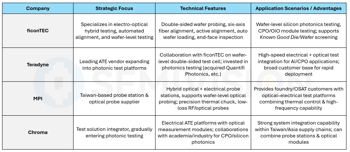
Key Highlights of GlobalWafers’ 12-inch SiC Wafer Technology
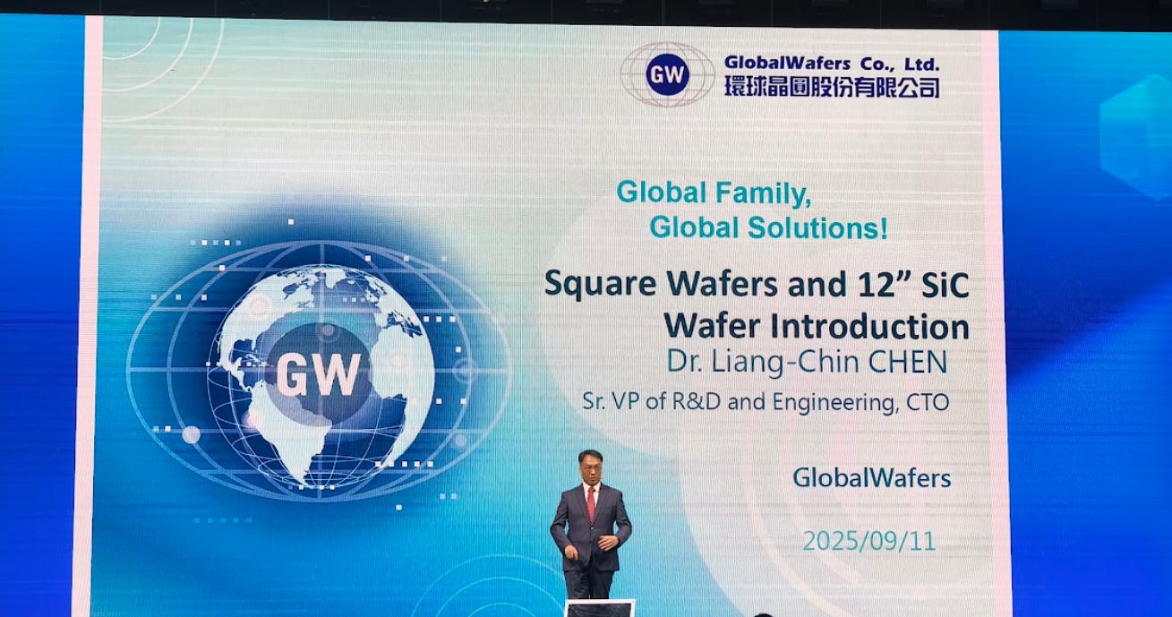
In mid-September, GlobalWafers unveiled a breakthrough technology showcasing the application of 12-inch SiC wafers, with a particular focus on SiC’s exceptionally high thermal conductivity. This announcement directly addressed the industry’s growing attention onSiC thermal management substrates.
Previously, there had been market speculation that SiC could be applied as a plating/coating layer for heat dissipation. However, experimental results revealed that although such methods could be integrated into the process, they suffered from poor heat transfer efficiency. The additional thermal resistance created at material bonding interfaces caused actual cooling performance to fall far short of expectations.
GlobalWafers explained that their new approach is closer to the concept of acarrier wafer: introducing a full SiC carrier wafer directly into the packaging process as the key structural and thermal conduction layer. This design dramatically reduces the interfacial thermal resistance issues seen in coating-based solutions, while leveraging SiC’s intrinsic high thermal conductivity (~490 W/m·K). The result ensures that the massive heat flux generated by GPU and HBM stacks can be effectively conducted and dissipated.
Separation of Electrical and Thermal Functions
In this new architecture, electrical conduction remains handled by the conventional silicon interposer, preserving mature interconnect performance and packaging compatibility. Meanwhile, the SiC carrier wafer is dedicated solely to heat dissipation, acting as a “thermal acceleration layer.” This division of labor between electrical and thermal roles not only lowers yield risks but also avoids disruptive changes to the established silicon interposer supply chain.

Effectively, this adds a SiC carrier substrate at the base of advanced packaging stacks, significantly improving vertical heat dissipation bottlenecks. Preliminary tests indicate that under high computational loads, this approach reduces thermal buildup and enhances the stability of AI GPUs. It is particularly well-suited for >1000 W-class HPC/AI server chips.

Supply Status and Large-Size Capability
Silicon wafers are the most mature and widely available. The industry has long established 200 mm and 300 mm (8- and 12-inch) wafers, and production at even larger diameters has been explored. With high yields, large-scale capacity, and relatively low costs, silicon remains the foundation of the semiconductor supply chain.
Glass substrates are also available in SEMI-standard formats. Materials such as fused silica, borosilicate, and aluminosilicate glass are already supplied in wafer form, with sizes up to 200–300 mm. These larger formats are widely applied in display panels and optical substrate fields, and are now drawing attention for potential roles in interposers and advanced packaging.
Silicon carbide (SiC) wafers are in an ongoing transition from 150 mm to 200 mm production, with early attempts at 300 mm under way. Supply remains limited to a handful of vendors, and the industry continues to struggle with yield and cost pressures, as defect density and wafer processing remain significant bottlenecks.
Aluminum nitride (AlN) wafer supply is even more limited than SiC. Most available formats remain at smaller diameters or in ceramic plate form. A few suppliers are pushing single-crystal AlN wafer technology, aiming to scale up size and improve crystal quality, but progress is slower compared with SiC.
Key Advantages and Challenges
Silicon offers the clear advantage of maturity: low cost, large wafer sizes, high yields, and a stable supply chain. Its limitations lie in relatively weak thermal conductivity and breakdown field compared to wide-bandgap materials, which restricts its use under extreme high-power, high-temperature, or high-frequency conditions.
Glass provides excellent insulation and optical transparency, with costs lower than most ceramics and strong electrical isolation. However, its low thermal conductivity, mismatched thermal expansion, and weaker durability at high temperatures or under mechanical stress limit its use in demanding power or thermal environments.
Silicon carbide stands out for its wide bandgap, high breakdown field, superior thermal conductivity, and ability to perform in high-temperature or harsh conditions. Its challenges, however, are significant: wafer yields, crystal growth cost, large-diameter scale-up, defect control, and matching coefficient of thermal expansion (CTE) with packaging materials.
Aluminum nitride combines high thermal conductivity with excellent insulation, a low CTE well-matched to silicon, and strong stability, making it highly suitable for power and RF packaging. Yet, high costs, difficulties in producing large single-crystal wafers, demanding polishing requirements, and yield/purity limitations remain major obstacles.
The Next Frontier of Chip Technology: Radical Innovation for Unprecedented Performance
As Moore’s Law approaches its physical limits, the focus of semiconductor innovation is shifting away from mere transistor scaling toward broader and more radical domains. SEMICON Taiwan 2025 showcased how the industry is exploring breakthrough technologies to overcome the challenges posed by AI and high-performance computing (HPC), with packaging and materials science taking on an unprecedented central role.
Diamond on Chip: A Revolution in Thermal Management
In a technical briefing on the next-generation TPU, one of the most striking—and even shocking—highlights appeared under thermal management:“Diamond on chip.”
2025年9月21日
The physics behind this concept is clear. Diamond possesses the highest known thermal conductivity of any natural material, making it theoretically the perfect medium for extracting heat from high-power AI chips. With AI chip power densities growing exponentially, thermal management has become the foremost bottleneck restricting performance.
Yet, applying diamond in semiconductor manufacturing is an immense engineering challenge. As one materials expert noted, diamond is also the hardest material in nature and extremely difficult to process. If diamond were to be used as an interposer or substrate, it would require vias to be formed—and only diamond tools can cut diamond. The cost could therefore be prohibitive.
Nevertheless, the very proposal ofdiamond on chipis more than just an engineering idea. It is a declaration of intent. It signals that the thermal challenges of AI have reached such extremes that materials once thought of as science fiction are now being seriously considered. Traditional cooling methods—air cooling and liquid cold plates—are nearing their physical limits. By openly presenting its investment in material breakthroughs, Google has signaled the start of a potential “exotic materials” arms race in thermal management and packaging. This could accelerate synthetic diamond manufacturing, advanced bonding techniques, and novel metrology tools. The center of innovation—and value creation—is clearly shifting from the front end (transistor scaling) to the back end (packaging and materials). Companies that master these new material sciences will gain decisive competitive advantages.
Packaging as the New Architecture
Beyond diamond cooling, the same slide deck revealed an integrated vision of future technologies that together sketch a blueprint for system design. These illustrate the industry’s most discussed themes at SEMICON Taiwan—heterogeneous integration, 3DIC, and chiplets—which are rapidly replacing Moore’s Law as the driving force of the industry.
Panel-Level Packaging (PLP):Transforms the production unit from circular 300 mm wafers to larger rectangular panels, unlocking economies of scale and enabling much larger package sizes.
3.5D Packaging:An evolution of today’s 2.5D CoWoS, integrating 3D-stacked chips (such as memory stacked on logic) into a large silicon interposer, thereby increasing density and bandwidth.
Silicon Photonics and 224G SerDes:Replacing electrical signals with optical links for chip-to-chip data transfer, dramatically boosting bandwidth and reducing power consumption—critical for building large, distributed AI systems.
Together, these technologies reflect a paradigm shift: the package is the system. Instead of striving for a single monolithic chip, the future lies in highly integrated, modular systems-in-package.
With the end of Moore’s Law, performance gains can no longer rely solely on shrinking transistors. They must come from architectural and integration innovation. PLP, 3.5D integration, and silicon photonics are the tools that enable more HBM stacks, more logic units, and faster I/O within an efficient package.
This transformation fundamentally reshapes the semiconductor value chain. The boundaries between foundries (e.g., TSMC), OSATs (e.g., ASE), and system design leaders (e.g., Google, NVIDIA) are blurring. Success will no longer hinge only on who owns the most advanced 2 nm process node, but on who masters the art of integration across chips, substrates, and interconnects. This creates vast opportunities for equipment and materials suppliers specializing in advanced packaging, while making it clear that future chip design will be inseparable from packaging design and system design.
Comparative Analysis of Next-Generation AI Accelerator Specifications
To more clearly illustrate the differences in technology roadmaps, the table below compares the publicly available specifications of Google’s next-generation TPU and NVIDIA’s Blackwell/Rubin platforms.
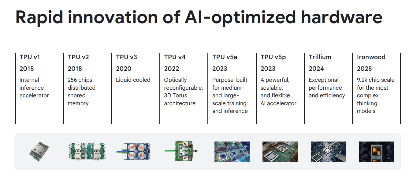
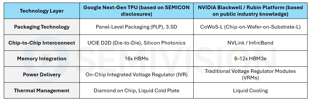
This comparison highlights the distinct emphases in each company’s technological bets. Google’s roadmap appears more aggressive and forward-looking, fully embracing next-generation innovations such as panel-level packaging, silicon photonics, and diamond-based thermal management. The goal is to achieve performance breakthroughs through system-level integration. In contrast, NVIDIA focuses more on optimizing and evolving around existing, mature technologies such as CoWoS, while leveraging its proprietary NVLink interconnect to reinforce its ecosystem.
The Invisible Battlefield: Geopolitics and the Weaponization of Materials
Beneath the noise of technology and market competition, a more hidden—but potentially more destructive—battlefield is emerging. During SEMICON Taiwan 2025, industry leaders warned that the global semiconductor supply chain is now overshadowed by geopolitics, with the supply of critical materials becoming the latest front in strategic rivalry.
First Alarm: “Choke Points” and National Security
At a pre-show press conference, GlobalWafers Chairwoman Doris Hsu issued a stern warning: the semiconductor industry’s newest challenge is the “weaponization” of critical materials.
She cited the well-known case of the 2019 Japan–Korea trade dispute. In response to historical compensation issues, Japan imposed export controls on three vital electronic materials—fluoropolyimide for OLED displays, photoresists for semiconductor manufacturing, and high-purity hydrogen fluoride. This hit South Korea’s electronics sector hard. The episode proved that material supply can shift instantly from a commercial matter to a geopolitical weapon.
At SEMICON, modern “choke points” were repeatedly discussed:
Gallium (Ga):Over 90% of global production is concentrated in China, which now enforces export permit controls. Gallium is essential for GaN power semiconductors and RF components, critical to 5G and EVs.
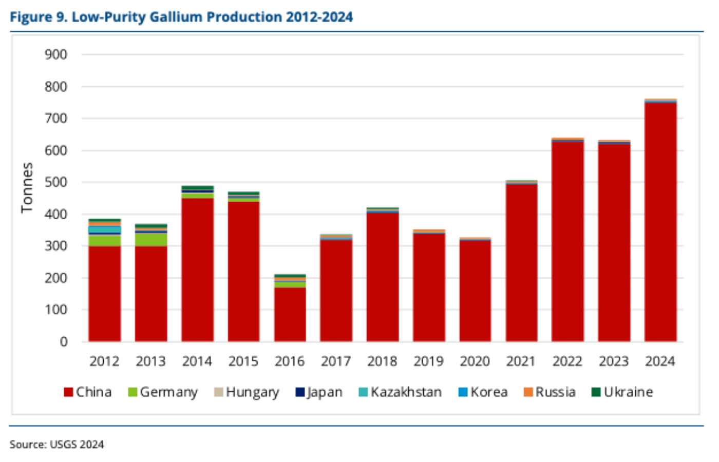
Low-CTE glass fiber cloth:The key reinforcement material in ABF substrates for AI accelerators, currently supplied exclusively by Japan’s Nitto Boseki. Its scarcity has been described as “the biggest bottleneck for all AI chips next year.”

2025年7月30日
The seriousness of the issue was confirmed by voices at the heart of the industry. Dr. Ho Jun, Vice President in charge of TSMC’s CoWoS business, remarked at the 3DIC Advanced Packaging Alliance launch:“Taiwan’s materials are too weak, and we risk being choked.”For such words to come from the world’s largest foundry underscored the severity of supply-chain vulnerability.
National Strategy and Industry Response
In the face of escalating risks, governments and industries are drafting counterstrategies. In Taiwan, calls are growing for a government-backed “national materials team” to boost self-sufficiency and reduce dependence on foreign sources. Doris Hsu’s public statement was widely seen as setting the stage for such an initiative.
Japan, meanwhile, is pursuing a more calculated approach. Professor Yasuhiko Ohta of Hokkaido University, author ofThe Geopolitics of Semiconductors, explained that Japan’s strategy is to secure “indispensability” in the supply chain. Even if Japan loses competitiveness in end products, holding monopoly positions in niche materials ensures leverage over the entire chain. The government is actively identifying materials where Japan holds absolute advantage, such as ultra-high-purity copper sputtering targets, and treating them as national strategic assets.
Nitto Boseki exemplifies this strategy. The company recently announced it would triple production of low-CTE glass fiber cloth, with nearly 20% of investment covered by subsidies from both central and local governments. Many in the industry suspect strings attached: the government is likely requiring Nitto to prioritize supply to Japan’s domestic semiconductor ecosystem, forging “materials-to-packaging” and “packaging-to-wafer” linkages—supporting Japan’s semiconductor revival through companies like Rapidus, which just announced successful 2 nm pilot runs.
The “weaponization of materials” is shifting the geopolitical focus of semiconductors from the location of advanced fabs (e.g., “Where is TSMC’s 2 nm plant?”) to a broader, more complex battle over the entire supply chain. SEMICON discussions revealed a deeper truth: controlling chip manufacturing alone is insufficient. Without critical chemicals, gases, and substrates, even the most advanced fab cannot operate. Nations like Japan, which have lost leadership in chip manufacturing, now recognize they can still exert strategic power by controlling indispensable inputs.
This dynamic is sparking a new wave of industrial policy and investment, emphasizing “reshoring” or “friend-shoring” of material production. Companies like TSMC and Samsung may be forced to diversify material sources—even at higher cost—to mitigate geopolitical risks. The result could be a less efficient but more resilient global supply chain, with redundant capacity spread across different geopolitical blocs. Ultimately, the costs of this resilience will be passed down to end consumers.
Analysis of Critical Material Choke Points
A dedicated risk matrix now translates the abstract threat of “material weaponization” into concrete vulnerabilities. It provides supply-chain managers and strategists with actionable intelligence, directly addressing the concerns raised by industry leaders at SEMICON.
Strategic Implications and Outlook
The trends revealed at SEMICON Taiwan 2025 represent not just technological evolution but a profound restructuring of industry dynamics and geopolitical competition. From this analysis, the next few years of the semiconductor sector are likely to show several defining features:
The rise of dual superpowers:The uncontested dominance of NVIDIA in AI hardware is ending. The future will be a duopoly: NVIDIA’s “general-purpose” empire built on CUDA and a broad customer base, and Google’s vertically integrated “full-stack” ecosystem spanning models to chips. Key metrics to watch include deployment volumes of next-gen TPUs versus NVIDIA’s Rubin, benchmark results, and—critically—the share of TSMC’s CoWoS capacity each commands.
Packaging and materials supremacy:Innovation and value creation are unmistakably shifting from front-end transistor scaling to back-end packaging and materials science. Companies and nations investing heavily here will hold the keys to future performance. The progress of technologies likediamond-on-chipcooling and panel-level packaging will serve as milestones of this shift.
Supply chain Balkanization:Driven by geopolitics, fragmentation will intensify. The specter of material weaponization will push nations to build regional, semi-autonomous supply networks. The question is no longerifthis division will occur, buthow quickly—and at what cost to global efficiency and innovation. Taiwan’s “national materials team” and Japan’s “indispensability” strategy will be crucial case studies.

SEMICON Taiwan 2025 will be remembered as a watershed moment. It crystallized the vision of the next decade: a multipolar, system-level, material-constrained era of competition. The battles of the future will be fought not only in the cleanrooms of fabs but also in materials labs and government halls. For every player in the industry, adapting to this new reality will be the only path to survival and growth.


PreviousNext
TopLatestDiscussions








See all