SiC Enters the Advanced Packaging Mainstage: Observing TSMC’s SiC Strategy
SiC Enters the Advanced Packaging Mainstage: Observing TSMC’s SiC Strategy
- Source: SemiVision
- Author: SEMIVISION
- Published: 2025-09-21T21:20:50+08:00
- URL: https://tspasemiconductor.substack.com/p/sic-enters-the-advanced-packaging SiC Enters the Advanced Packaging Mainstage: Observing TSMC’s SiC Strategy


Observing TSMC’s SiC Strategy :SiC Enters the Advanced Packaging Mainstage
Original Articles By SemiVision Research (Nvidia ,TSMC, Globalwafers, Wolfspeed)

Sep 21, 2025
∙ Paid

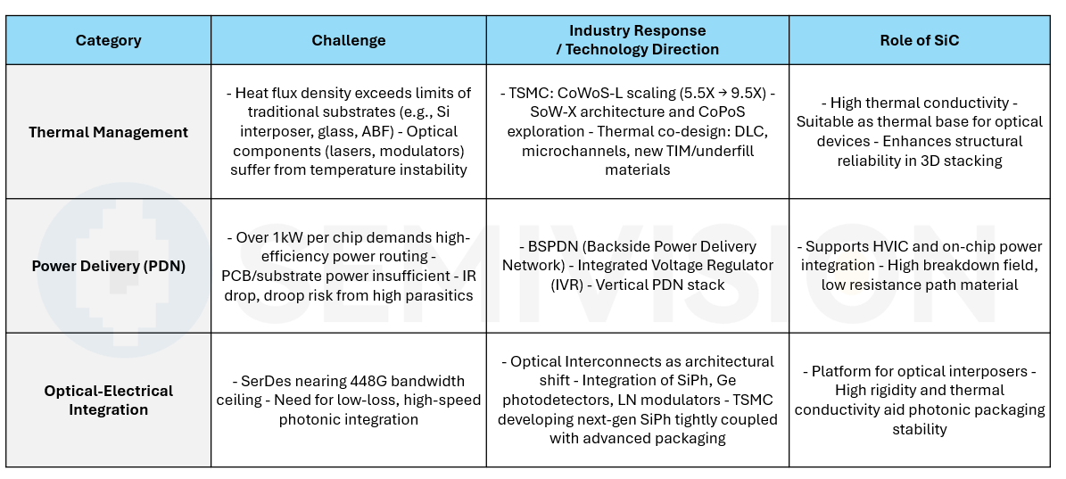
As the complexity and power demands of AI chip designs continue to escalate, Power Delivery Networks (PDNs)and thermal management have emerged as unavoidable core challenges for the industry. Traditional power delivery through PCBs or ABF substrates is becoming increasingly inadequate due to long power paths and high parasitic inductance, leading to IR drops and transient voltage droops. With single GPUs now requiring over 1000A of current, these legacy approaches are approaching their limits.
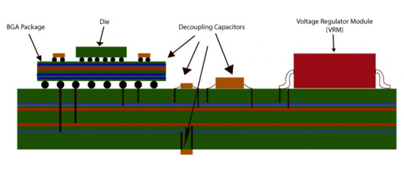
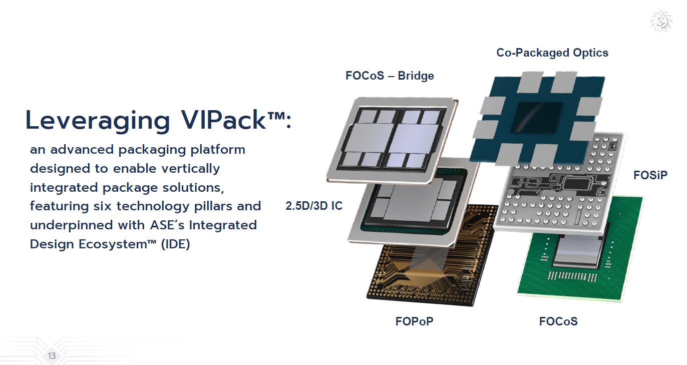
To address these challenges, foundries and OSAT (Outsourced Semiconductor Assembly and Test) providers are actively proposing solutions across different integration levels. For instance, Marvell has introduced the PIVR (Package-Integrated Voltage Regulator), embedding the VRM directly into the package to shorten the power path and reduce PDN impedance, enabling faster voltage response. ASE, through its VIPack and FOCoS-Bridge (with TSV) platforms, is optimizing PDN, signal interconnects, and thermal performance simultaneously—especially for Chiplet + HBM packages that demand high bandwidth and I/O, enabling reduced power loss without compromising performance.
TSMC, on the other hand, is pursuing a more diversified integration strategy. In its CoWoS-L platform, TSMC embedsIVRsandeDTCs(embedded Deep Trench Capacitors) to enhance on-die decoupling density and power stability, while also developing BSPDN (Backside Power Delivery Network) to physically separate power and signal layers. This reduces voltage drop and frees up valuable front-side routing resources. TSMC is also pioneering thermal co-design, incorporating Direct Liquid Cooling (DLC), microchannel technologies, and exploring new materials for TIM (Thermal Interface Material) and underfill, with the goal of enabling reliable operation of kilowatt-class AI chips.

Under these trends,NVIDIA and other hyperscalersare beginning to viewmaterialsas a critical pillar in AI chip and system design, actively pushing the supply chain to explore diversified material options. Among these,Silicon Carbide (SiC)has suddenly become a focal point of attention.
Proven over the past three decades in the power electronics sector,SiChas emerged as a star material due to itswide bandgap (WBG),high thermal conductivity,high breakdown field strength,excellent thermal stability, andhigh Young’s modulus. It has already been successfully commercialized in electric vehicle inverters, industrial power modules, and high-voltage grid systems. Now, with the explosive growth in AI computing demand, SiC’s role is rapidly expanding intoadvanced packaging and heterogeneous integration.

SiC holds the potential to become thesubstrate material for high-voltage ICs (HVICs)andon-chip power delivery, supporting developments inBSPDNandIVRarchitectures. It also shows great promise as anoptical interposer, offering a thermally conductive, low-loss platform forsilicon photonics (SiPh)andlithium niobate (LN) modulators. Furthermore, its high rigidity and thermal conductivity are beneficial for large-area3D stacking of Chiplets and HBM, helping reduce package warpage while enhancing mechanical reliability.
These unique properties positionSiC as a key material linking PDN, thermal, and optical interconnect domains, driving strong investment and development efforts from the Taiwanese supply chain. The goal: to establish new industrial advantages in the age of AI and HPC.
Driven bygenerative AIandlarge-scale model training, companies likeNVIDIA,AMD,Google, andAWSare successively launching ultra-large-scaleGPUs and ASICspriced at tens of thousands of dollars each. These chips contain hundreds of billions or even trillions of transistors, with power consumption often exceeding1 kW—placing demands onthermal management,power delivery, andsignal interconnectsthat far exceed those of traditional HPC and server chips.
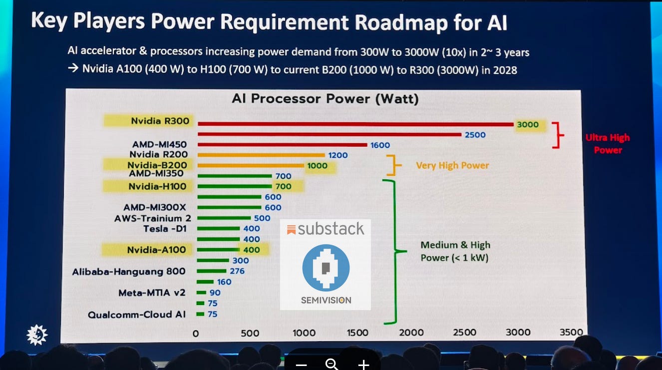
This exponential growth has revealed three critical bottlenecks in process and packaging technologies:
Thermal Challenges:
AI chips now generateheat flux densitiesthat push conventional thermal interface and substrate materials to their limits. Whether it'ssilicon interposers,glass cores, orABF substrates, existing materials are increasingly unable to meet the thermal conductivity and long-term reliability requirements.
This challenge also extends tooptical componentssuch aslasersandmodulators, whose performance is highly temperature-sensitive—minor thermal fluctuations can lead to bandwidth degradation and system-level errors. To tackle these thermal limitations,TSMCis focusing on evolving itsCoWoS-Lplatform throughreticle scaling, expanding package sizes from5.5X to 9.5Xto support higher integration density. TSMC is also advancing itsSoW-X (System on Wafer)architecture to further enhance 3DFabric integration, while exploringCoPoS (Chip on Panel on Substrate)and other ultra-large-area packaging technologies to open up new possibilities for3D integration and heterogeneous packaging.
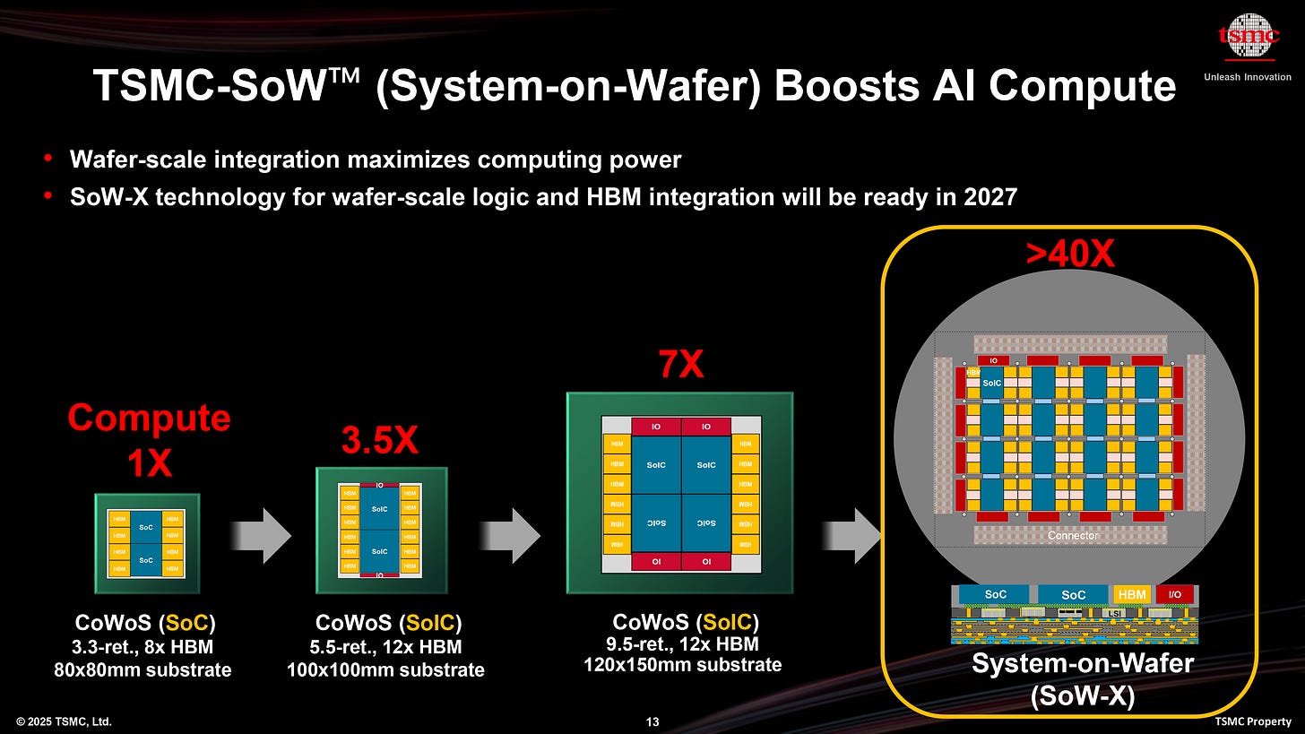
These strategies reflect TSMC’s comprehensive response to AI/HPC power and thermal demands—advancing acrossmaterials,architectures, andprocess nodes.
Power Delivery Bottlenecks:
As AI chip power demands rise, power delivery through packaging layers or PCBs alone is no longer sufficient.Backside Power Delivery Networks (BSPDNs),Integrated Voltage Regulators (IVRs), andvertical power delivery architecturesare becoming essential. These approaches require substrate materials withhigh voltage enduranceandlow-resistance conductioncapabilities.
Electro-Optical Integration Demands:
To overcome the physical limits ofSerDes bandwidth,optical interconnectshave become a critical direction for AI chip architecture. Efficient integration ofsilicon photonics (SiPh)components,germanium photodetectors, andlithium niobate (LiNbO₃, LN) modulatorswith logic chips and high-bandwidth memory is essential for advancing3D packaging and heterogeneous integration. According to SemiVision, current SerDes technologies are hitting a ceiling at448G, and breaking through this limit will requirenext-generation photonic materials and platforms. TSMC is now actively developingnext-gen silicon photonicsto meet the extreme bandwidth, latency, and power efficiency requirements of AI/HPC systems—while tightly integrating this with advanced packaging, forming a newelectro-optical architecture.
As artificial intelligence (AI) and high-performance computing (HPC) drive explosive demand for memory bandwidth, chip interconnect density, and power-thermal management, the traditional monolithic silicon SoC architecture and the size limits of silicon interposers have increasingly become bottlenecks in system design. TSMC’s 3DFabric strategy addresses these challenges through diversified packaging solutions such as InFO, WMCM, and SoW, with the CoWoS family at the forefront—focusing on how to integrate high I/O density, low latency, efficient heat dissipation, and robust reliability within advanced packages.
In CoWoS-S, the use of silicon interposers combined with TSVs provides exceptional signal and power integrity. However, once the interposer size surpasses the reticle boundary, yield and mechanical fragility risks rise sharply. To mitigate these limitations, CoWoS-R introduces an RDL-based organic interposer architecture, leveraging polyimide/polymer dielectrics with fine copper routing to redistribute signals and power. This not only sustains strong electrical performance but also alleviates thermal expansion mismatches and mechanical stress. Building on this, CoWoS-L integrates local silicon interconnect dies with higher-order RDL structures, enabling ultra-large interposers and more complex chiplet-HBM integration for future AI/HPC designs.
Recently, breakthroughs in materials have emerged as a potential game-changer. TSMC is exploring the use of single-crystal silicon carbide (SiC) as an interposer or substrate, aiming to capitalize on SiC’s superior thermal conductivity and mechanical robustness to enhance heat dissipation and reliability, while overcoming the inherent size and material limitations of silicon interposers. At the same time, panel- and PCB-level packaging approaches such as CoWoP and CoPoS are surfacing as complementary or competitive alternatives to CoWoS, particularly for large-form-factor, cost-sensitive markets that still demand high performance.
This article will systematically examine the role of RDL in the CoWoS family with respect to power integrity, signal integrity, reliability, and stress control, assess the feasibility of SiC as an interposer or substrate, and evaluate whether emerging form factors such as CoPoS and CoWoP may redefine the trajectory of TSMC’s 3DFabric ecosystem.
For Paid Members, SemiVision will discuss topics on
The Role of SiC: A Cross-Domain Enabler
The Value of SiC in Optical Waveguides
Development Background of SiC Waveguides for AR Glasses
Broadband Single-Mode Planar Waveguides in Monolithic 4H-SiC (Bosma et al.)
Racetrack Microresonator-Based EO Phase Shifters on a 3C-SiC-on-Insulator Platform
SiC Substrate-Integrated Waveguides for High-Power MC above 110 GHz
Emerging SiC Applications Beyond Power Electronic Devices (La Via et al.)
Possible Layout of Passive and Active Components in an Optical Interposer (SiC)
Possible Layout of Passive and Active Components in an Optical Interposer (SiC)
Familiarity of SiC in Foundry Equipment
Why TSMC Think about the opportunities and challenges of SIC issues
Intersection of SiC and TSMC Advanced Packaging: Material Properties, Supply Chain, AI Mega-Chip Demands, and Strategic Outlook
Core Value of SiC in Packaging Applications
Next Phase: 12-inch SiC Wafer Breakthrough
Wolfspeed’s Business Challenges and the Rise of China’s SiC Industry
Global Competitive Landscape
TSMC’s Role in 12-inch SiC Adoption
6-inch Era: The Starting Point for Power Electronics
8-inch Era: Cost Scaling and Supply Chain Expansion
Market Size Forecast
Core Requirements of AI Megachips: Thermal, Power, Optical, and 3D Integration
Competitive Strategies: Intel vs. Samsung
Challenges of 12-inch SiC: Yield, Cost, and CTE Mismatch
The Role of SiC: A Cross-Domain Enabler
In the midst of these three converging challenges,Silicon Carbide (SiC)is emerging as apotential ultimate solutiondue to itshigh thermal conductivity,mechanical strength, andwide bandgapproperties. SiC is not only a candidate forthermal substrates, but also for:
Optical interposers
Electrical interposers
Vertically integrated power delivery platforms
HVIC (High-Voltage Integrated Circuit) support layers
This positions SiC as ahybrid integration enabler, capable of linking power delivery, thermal dissipation, and optical interconnects into a unified platform.
As the world’s largest foundry and a leader in advanced packaging, TSMC is proactively exploring this material transition.Its platforms—CoWoS, SoIC, and InFO—have already established a robust ecosystem for high-performance packaging. More recently, TSMC introduced theCOUPEplatform, offering a clearer strategic vision for the development of large-scale AI chips:
Electro-optical Integration:
Integrating components such assilicon photonics (SiPh),lithium niobate (LN)thin films, andlasersat the packaging level to reduce optical interconnect latency and power consumption.
Vertical Power Delivery:
CombiningBSPDN (Backside Power Delivery Network)with on-die inductors and capacitors to shorten power transmission paths and enhance PDN efficiency.
Heterogeneous Integration:
Utilizing3D packagingandchiplet architecturesto stack logic, memory, and photonic components in a tightly integrated form.
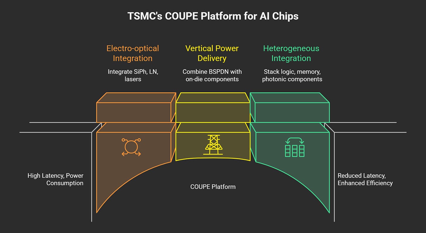
If SiC substrates are introduced into COUPE or future platforms like CoWoS-Next or SoIC-X, TSMC could be the first to simultaneously address the triad of thermal, electrical, and optical challenges, thereby creating a unique competitive edge in AI packaging. This move would not only shift material choices but also reshape the entire AI semiconductor supply chain.
Meanwhile, Intel is actively advancing PowerVia backside power delivery and Foveros/EMIB technologies, while Samsung is investing heavily in HBM stacking and glass core substrates. In comparison, if TSMC succeeds in bringing SiC into mass production, it could establish a commanding lead in thermal management and electro-optical integration.
Currently, industry sources report that NVIDIA is collaborating with TSMC to explore SiC as an interposer material, aiming to meet the increasing bandwidth and power demands of AI/HPC packaging. However, whether this approach can be successfully commercialized remains to be seen, as SiC still faces uncertainties in cost, process maturity, and large-die wafer yield.
Currently, in addition toNVIDIA, which is actively exploring the use ofceramic materials,AMDis reportedly pursuing similar ideas. However, the two companies differ in theirmaterial selection strategies.
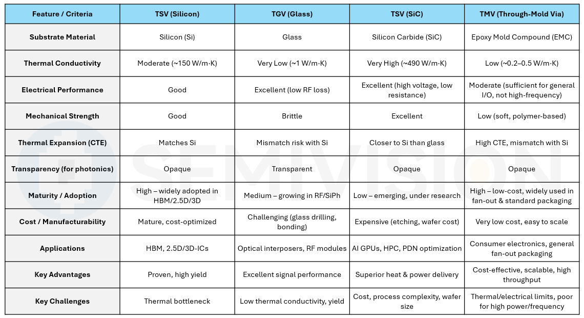
Looking at the current roadmap for advanced packaging technologies,vertical interconnect (via)solutions remain at the core:
TSV (Through-Silicon Via):
The most mature and widely adopted solution, especially for2.5D/3D stackingandHBM (High Bandwidth Memory)integration.
TGV (Through-Glass Via):
Usesglassas a substrate, offeringlow signal lossandlow thermal expansion, making it suitable forlarge-area substrates. However, improvements inprocess yieldandreliabilityare still ongoing.
TMV (Through-Mold Via):
Alow-costsolution implemented throughmolding technology, commonly used insubstrate-level packaging, well-suited forhigh-volume production.
TSV (SiC):
A recent focus in the industry. LeveragingSilicon Carbide's (SiC)highthermal conductivityandvoltage tolerance, this approach aims to overcome thermal andPDN (Power Delivery Network)bottlenecks present in traditional silicon or glass substrates.
At the cutting edge of research, SemiVision has identified multiple papers presented at IEEE and other international academic conferences evaluating the feasibility of TSV (SiC). These studies cover topics such as power integrity, thermal management, and reliability analysis, and the results suggest that SiC has real potential as a packaging substrate—particularly for high current density and large-scale AI chip PDN optimization.
Meanwhile, TSMC has also demonstrated a clear direction in its patent portfolio, with several patents focusing on the integration of SiC substrates with TSV structures. These filings emphasize how SiC can improve both PDN conductivity and thermal dissipation, further supporting the high-power demands of next-generation AI GPUs.
Although theSiC interposerhas clearstrategic potential, mass production requires overcoming three key challenges:
Defect density controlin large-size SiC wafers
Process compatibilitywith existing TSV/TGV technologies
Cost structure and yield improvement
The resolution of these issues will directly determinehow quickly and broadly SiC can be adopted in NVIDIA’s and TSMC’s advanced packaging roadmaps.
The Value ofSiC in Optical Waveguides
Waveguide Technology Best Suited for AR Glasses Design Goals
Currently, the optical solutions for AR glasses include freeform optics, BirdBath, and optical waveguides. Among them,diffractive optical waveguidesare considered one of the most promising technologies. Because they are compact, lightweight, and transparent, they can be used to make AR glasses with an appearance similar to traditional eyewear.
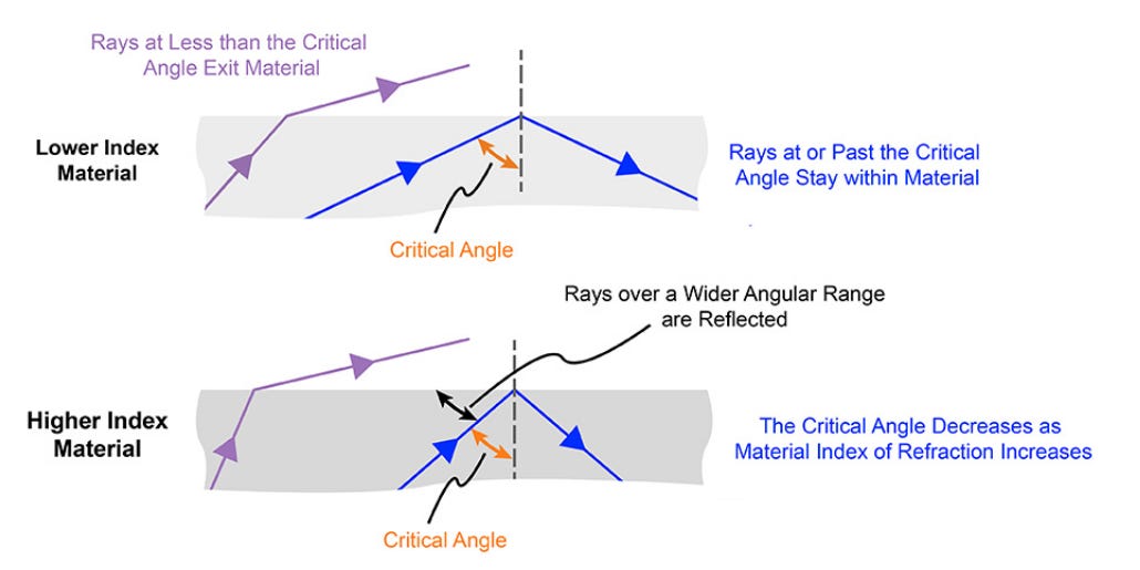
A diffractive waveguide works by utilizing the principle ofTotal Internal Reflection (TIR), which traps light within the material itself, like a tiny transparent tunnel, guiding light from the display to the viewer’s eyes.
When light enters from a denser material (such as glass) into a less dense medium (such as air),TIRoccurs. When the angle of incidence at the boundary between the two materials is sufficiently large, the light will be completely reflected back. The angle at which this reflection occurs is called the“critical angle.”The higher the refractive index of the material, the smaller the critical angle becomes. This is the working principle of waveguide lenses.
Development Background of SiC Waveguides for AR Glasses
In AR head-mounted devices based on waveguide technology, light from the display enters the edge of the waveguide through a coupler, propagates within the waveguide viaTotal Internal Reflection (TIR), and exits at the position of the out-coupler to reach the user’s eye.
As the refractive index of the material increases, TIR can occur at smaller incident angles. In other words, the higher the refractive index, the wider the range of incident angles that can be internally reflected, thereby enabling awider field of view (FOV).

FOV is the key to enhancing immersion in AR glasses. Using waveguide materials with a higher refractive index can expand the FOV.
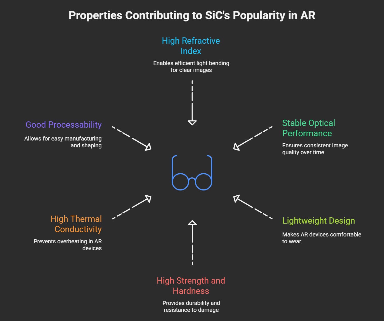
In the optical systems ofAR glasses,diffractive waveguidesare one of the most promising display technologies, capable of delivering a widefield of view (FOV)while significantly reducing lens thickness—bringing AR devices closer to the form factor of ordinary eyeglasses. Traditionally, waveguide materials have beenglass or resin, with refractive indices around1.8–2.0, limiting the tradeoff between wide FOV and lightweight modules. By contrast,Silicon Carbide (SiC), with itshigh refractive index (2.6–2.7), offers unique advantages for optical waveguide applications.
First, under the same design conditions, anSiC waveguidecan achieve anultra-wide 70°–80° FOVwith asingle-layer structure, while keeping the lens thickness at only~0.55 mmand the weight at just2.7 g, significantly reducing the wearing burden. Second, SiC’s high refractive index and excellent optical uniformity effectively mitigate the long-standing issue of“rainbow effects”in diffractive waveguides, greatly improving display purity and image quality.
In addition, SiC’shigh thermal conductivity (~490 W/m·K)allows it to efficiently dissipate the heat generated byMicro LED light sourcesduring high-brightness operation, ensuring stable optical performance. Itsextreme hardness (Mohs 9.5)also provides outstanding scratch resistance and durability, meeting the long-term, everyday use requirements of consumer-grade products.
Taken together, applyingSiC to optical waveguidesaddresses multiple challenges in AR glasses, includinglightweight design, extended battery life, high-definition display, and durability. This makes SiC widely regarded as akey breakthrough material. Consequently, the combination of“Micro LED + SiC waveguide”is increasingly seen as the mainstream technological pathway for future AR displays, accelerating the industry’s march towardscalability and maturity.
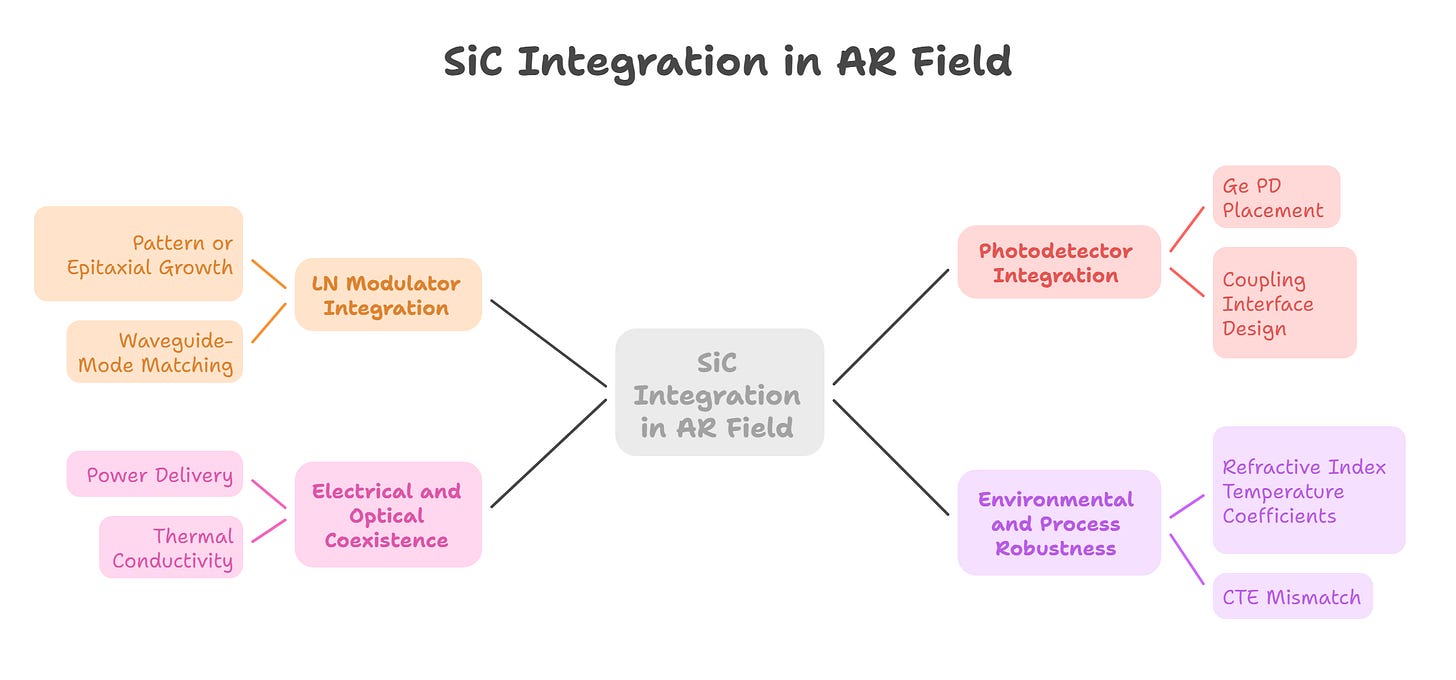
The concept of applyingSiC materialstowaveguides and interposersis not only feasible but also indispensable in high-frequency, low-loss heterogeneous integration. Here, the interposer should be regarded as anOptical Interposer, with one of its core functions being to supportpassive optical signal transmission through SiC waveguide structures, while integratingactive componentswhere needed—such asGe or III-V photodetectors (PDs)compatible with MOS/CMOS, andelectro-optic modulators (EOMs)based onlithium niobate (LN)or LN thin films.
In practice, this can be implemented as follows:
Integration of LN Modulator on SiC Waveguides
Pattern or epitaxially grow an LN modulator structure inside the SiC waveguide (or use heterogeneous bonding/film transfer).
Achieve phase or intensity modulation with waveguide-mode matching to minimizeVπ·Lπand increase bandwidth.
Integration of Photodetectors (PDs)
Place detectors such as Ge PDs at the waveguide end or branch points to receive modulated optical signals.
Careful coupling interface design is critical: mode-size converters, tapers, reflective mirrors, or graded-index structures can reduce coupling loss.
Coexistence of Electrical and Optical Architectures in the Interposer
Power delivery, driver signal lines, and passive/active components (e.g., decoupling capacitors) should be arranged in layers or regions that do not conflict with the optical waveguide.
LeverageSiC’s high thermal conductivityfor heat dissipation, and design appropriate thermal structures close to active devices to minimize modulation and detection errors caused by temperature fluctuations.
Environmental and Process Robustness
Address challenges such as differences in refractive index temperature coefficients between SiC waveguides and LN/PDs, coefficient of thermal expansion (CTE) mismatch, packaging-induced mechanical stress, optical scattering and waveguide surface roughness, as well as fabrication precision of surfaces and sidewalls.
ThisOptical Interposer architecturecan significantly improvebandwidth, latency, and power efficiencyin AI/HPC systems:
Lower loss compared to pure electrical interconnects
Shorter coupling distance compared to passive optical waveguides plus external modules
Better balance of thermal and electrical performance compared to conventional interposers
As the integration and manufacturability ofSiC waveguides with LN modulators and photodetectorsmature, thishybrid architectureis highly likely to become the mainstream direction forCo-Packaged Optics (CPO)andOptical I/Oin futureAI GPU/ASIC platforms.
These keywords and technologies are connected in the following ways:
SiC (Silicon Carbide):
A wide-bandgap semiconductor material, highly valuable in power electronics and RF/high-frequency applications because of its high voltage tolerance, high-temperature resistance, and lower loss. Historically, it has been used inpower devices,EVs,chargers, andindustrial equipment. In some semiconductor forums in China, diagrams have shown mentions of using“waveguide/interposer” with SiC, which suggests applying SiC ininterposer layers or waveguide structuresto carry optical/electrical signals.
Waveguide:
Waveguides can beoptical waveguidesorRF waveguides, designed to transmit optical or RF signals. UsingSiC as a waveguide materialcould targetRF, millimeter-wave, or terahertz applications, such as5G/6G,small base stations,radar,automotive sensors, andsatellite communications.
Interposer:
Interposers are widely used in2.5D/3D packagingto closely connect different chips, wafers, or chiplets. Their roles include shortening signal transmission paths, enablinghigh-speed I/O, and handlingpower/signal distributionwithin the package. Traditional interposers are often made ofsilicon (Si)orglass, though other materials are sometimes adopted.
8-inch / 12-inch (ø200mm / ø300mm) SiC wafers for waveguide/interposer applications:
Many recent studies support these requirements, highlighting the feasibility of integrating bothactive and passive optical components(e.g., LN modulators, Ge/III-V photodetectors) into aSiC-based optical interposerfor AI/HPC applications.

Broadband Single-Mode Planar Waveguides in Monolithic 4H-SiC (Bosma et al.)
Waveguides andp-i-n structuresfabricated in monocrystalline4H-SiCcan be used for optical signal transmission and color center control with low loss.
This work demonstrates thatSiC optical waveguidescan operate in the near-infrared/visible band and can be integrated with electronic components (e.g., p-i-n structures). This aligns with the concept of aSiC optical interposercombining bothpassive and active elements.
Racetrack Microresonator-Based EO Phase Shifters on a 3C-SiC-on-Insulator Platform
On a3C-SiC-on-insulator platform, racetrack-shaped microresonators have been fabricated aselectro-optic (EO) phase shifters.
This represents a form of active modulator. Although current performance (e.g.,Vπ·Lπ) has not yet reached commercial state-of-the-art levels, it shows the potential of SiC as amodulator material.
SiC Substrate-Integrated Waveguides for High-Power MC above 110 GHz
Substrate-integrated waveguides (SIW)fabricated onSiC wafersshow low loss and high power-handling capabilities, suitable formicrowave/millimeter-wave frequenciesabove 110 GHz.
This demonstrates that SiC can serve as both asubstrate and waveguide structurefor high-frequency signal applications—not just for passive transmission. Such SIW structures overlap in potential with theinterposer + waveguidefunctionality you described.
Emerging SiC Applications Beyond Power Electronic Devices (La Via et al.)
Explores thematerial and structural requirementsof SiC in optical waveguides and photonic applications—for example,SiC-on-insulator (SiCOI) stacksand exposing waveguides to low-index cladding materials for optical confinement.
It highlights thatSiC optical waveguidesmust ensure good index contrast (vs. SiO₂ or air), and thatthickness, surface roughness, and waveguide fabrication quality(etching, polishing) are key. These factors are also essential for integrating LN modulators or photodetectors.
Possible Layout of Passive and Active Components in an Optical Interposer (SiC)
Passive Waveguides:
SiC core surrounded by low-index cladding (e.g., SiO₂ or air trenches) to form optical confinement.
Waveguide cross-sections are typicallysub-micronto ensure single-mode propagation.
Functions: routing, splitters, filters, micro-ring resonators.
Active Modulator (LN / EO Modulator) Integration:
IntegrateLN thin filmsor chips with SiC waveguides usingmicro-transfer printingorheterogeneous bonding.
Structures can beMach–Zehnderormicro-ring, providing phase or amplitude modulation.
Drive voltage and bandwidth must align with SiC waveguide/interposer optical loss and dispersion characteristics.
Photodetector (PD) Integration:
Ge or III-V materials (e.g., InGaAs) can be fabricated as PDs and flip-chipped onto SiC waveguide ends.
Key considerations: optical-electrical coupling loss, latency, and power consumption.
Critical interfaces include fiber coupling, mode converters, and tapered waveguides.
Familiarity of SiC in Foundry Equipment
InCMP (Chemical Mechanical Polishing)processes, achieving a high-planarity surface often requires removing metal layers (Cu, W, Al) or dielectric layers (SiO₂, SiN). Over-polishing risks damaging underlying structures.
SiC as a Stop Layer:
Due to its high chemical inertness,SiC has an extremely low removal ratein common CMP slurries, effectively preventing damage to underlying materials.
With high hardness and superior mechanical selectivity compared to SiO₂/SiN, SiC enables precise process control inCu CMPorSTI CMP.
SiC also serves as abarrier layer, significantly suppressing Cu diffusion, making it ideal for Cu damascene structures—improving BEOL reliability.
Applications includeCu damascene CMPand integration oflow-k dielectrics with Cu interconnects, where SiC or SiCN variants reduce RC delay while serving as a stop layer.
SiCN in Advanced Packaging (Hybrid Bonding)
InHybrid Bonding(die-to-die or wafer-to-wafer direct bonding),SiCN plays a key role.
This technology is central to3D ICs, HBM, SoIC, and co-packaged optics (CPO).
Functions of SiCN:
Deposited above Cu pads to prevent oxidation and diffusion.
Acts as astop layerduring CMP opening to avoid over-polish damage.
Tunable refractive index and dielectric constant, suitable as a low-k dielectric protection layer.
Helps reduce thermal stress and stress migration, enhancing reliability.
Industrial Applications:
TSMC’sSoICand Intel’sFoverosincorporate SiCN in hybrid bonding pad designs.
In HBM stacks, SiCN strengthens die-to-die interface reliability.
InCPO/OIO (Optical I/O), SiCN protects photonic device electrodes, reduces interface loss, and supports high-speed interconnects.
SiC and SiCN are not just power electronics materials—they are emerging as key enablers for optical interposers, photonic integration, and hybrid bonding in AI/HPC packaging.
Why TSMC Think about the opportunities and challenges of SIC issues
Therefore, this report will take theintersection of SiC and TSMCas its core focus, and conduct an in-depth exploration of the following topics:
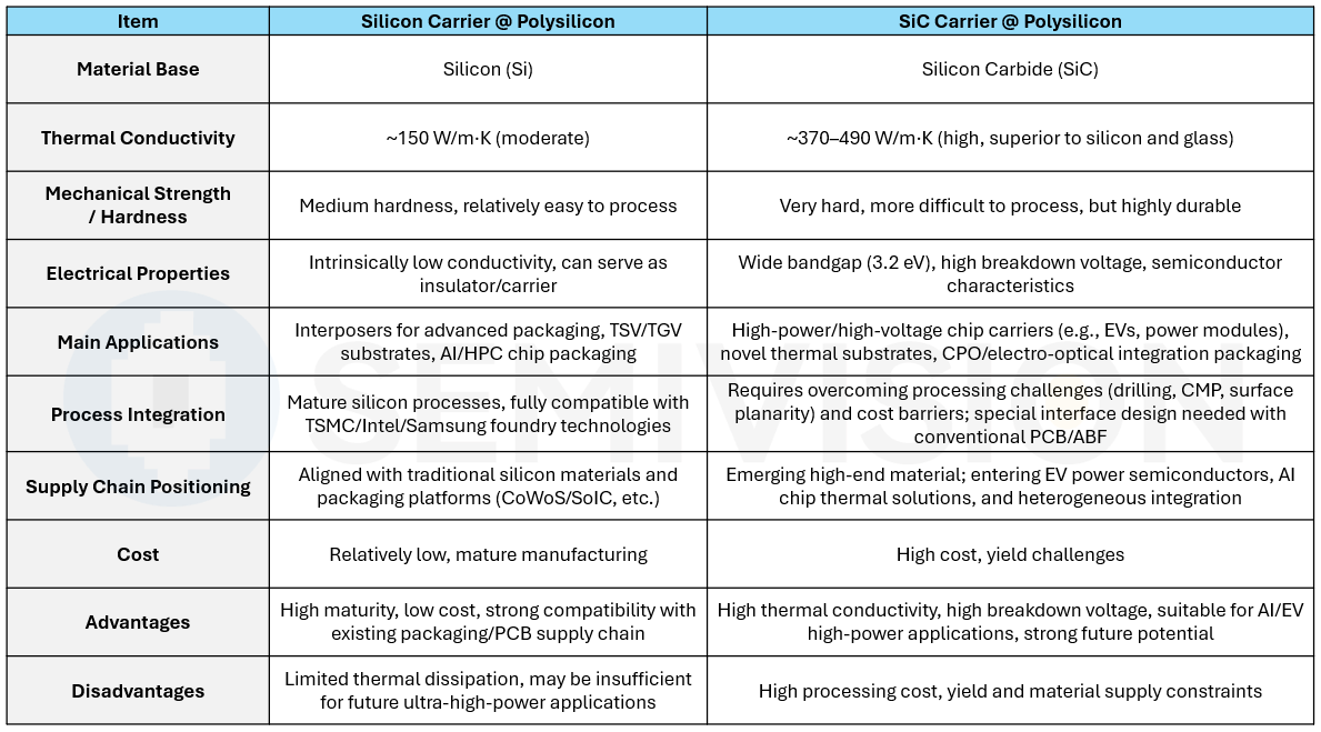
Material properties of SiC and a comparison between single-crystal and polycrystalline forms;
Technological progress and current supply chain status of12-inch SiC wafers;
Core requirements of AI mega-chips in thermal management, power delivery, and optical interconnects;
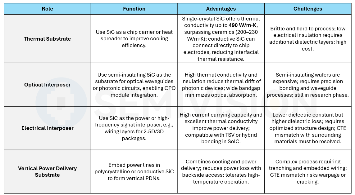
Thefour major rolesof SiC in advanced packaging: thermal substrate, optical interposer, electrical interposer, and vertical power delivery substrate;
Alignment between TSMC’s platforms (CoWoS, SoIC, COUPE) and SiC;
Strategic comparison with competitors such asIntel and Samsung;
Future market scale and strategic implications.
Through the above analysis, we will see that silicon carbide is no longer just synonymous with the power electronics era, but is gradually becoming the core substrate material of the AI boom era. In this process, TSMC is not only a technology driver but could also become the central integrator of the entire industry ecosystem.

Intersection of SiC and TSMC Advanced Packaging: Material Properties, Supply Chain, AI Mega-Chip Demands, and Strategic Outlook
Artificial Intelligence (AI) training and inference models are expanding at an astonishing pace, posing unprecedented challenges for chip power consumption, thermal management, and interconnect bandwidth. On one hand, increasing computational density has driven chip power consumption to several hundred watts or even beyond a kilowatt. On the other hand, data centers are striving to reduce energy consumption and latency, fueling the rise of new interconnect technologies such asco-packaged optics (CPO). To strike a balance between performance, power, and cost,advanced packaging technologiesare playing a pivotal role. While silicon-based packaging remains mainstream, the limitations of silicon in thermal conductivity and dimensional scalability are becoming more evident, pushing leading foundries such asTSMCto explore wide-bandgap (WBG) materials likesilicon carbide (SiC)as packaging substrates or interconnect layers.

This report focuses on the“intersection of SiC and TSMC”, systematically examining:
SiC material properties
12-inch SiC wafer technologies and supply chain status
Thermal and power delivery requirements of AI mega-chips
The four major roles of SiC in advanced packaging
Alignment between TSMC’s platforms and SiC
Competitor strategies
Challenges of 12-inch SiC (yield, cost, CTE mismatch)
Future market scale and strategic implications
Silicon Carbide (SiC) Material Technology Foundation
As one of the representativewide-bandgap semiconductors (WBGs),silicon carbide (SiC)was initially applied mainly in high-voltage, high-currentpower electronics. However, with the continuous growth in the scale and power consumption ofAI/HPC chips, SiC has increasingly emerged as a promising candidate material for advanced semiconductor packaging and substrates, thanks to its superior physical properties.
To understand the potential of SiC in AI mega-chip packaging, it is first necessary to review itsmaterial fundamentalsand contrast them with other mainstream substrate materials.
Material Properties of SiC
Bandgap and Breakdown Field
Wide Bandgap:The bandgap of 4H-SiC is about3.2 eV, significantly wider than silicon (1.1 eV) and gallium arsenide (1.4 eV), which translates into higher voltage endurance.
Breakdown Field:SiC has a breakdown field of about3 MV/cm, more than ten times that of silicon. This is why SiC-based power devices can withstand voltages from hundreds to thousands of volts.
Value in Packaging Applications:The high breakdown field makes SiC suitable as a substrate forvertical power delivery (BSPDN, HVIC), preventing leakage or breakdown under high voltage conditions.

Thermal Conductivity
SiC’s thermal conductivity ranges between370–490 W/m·K(depending on polytype and purity), which is much higher than silicon (150 W/m·K) and glass (0.9–1.5 W/m·K).
Compared to copper (~400 W/m·K) and diamond (>1000 W/m·K), SiC falls short of diamond but combinessemiconductor processabilitywith strong heat conduction.
Application in AI Chip Cooling:This property is sufficient to support the heat dissipation ofhundreds-of-watts GPU dies, providing a strong reason to replace Si interposers or ABF substrates.
Mechanical Strength and Thermal Expansion
SiC’sYoung’s modulusreaches410 GPa, with hardness second only to diamond, meaning it can withstand the mechanical stress ofmulti-layer stacking and large-area dies.
Itscoefficient of thermal expansion (CTE)is about4.0 ppm/K, between silicon (2.6 ppm/K) and copper (16.7 ppm/K). While this creates challenges for heterogenous integration, they can be addressed withbuffer layersandlow-stress bonding techniques.
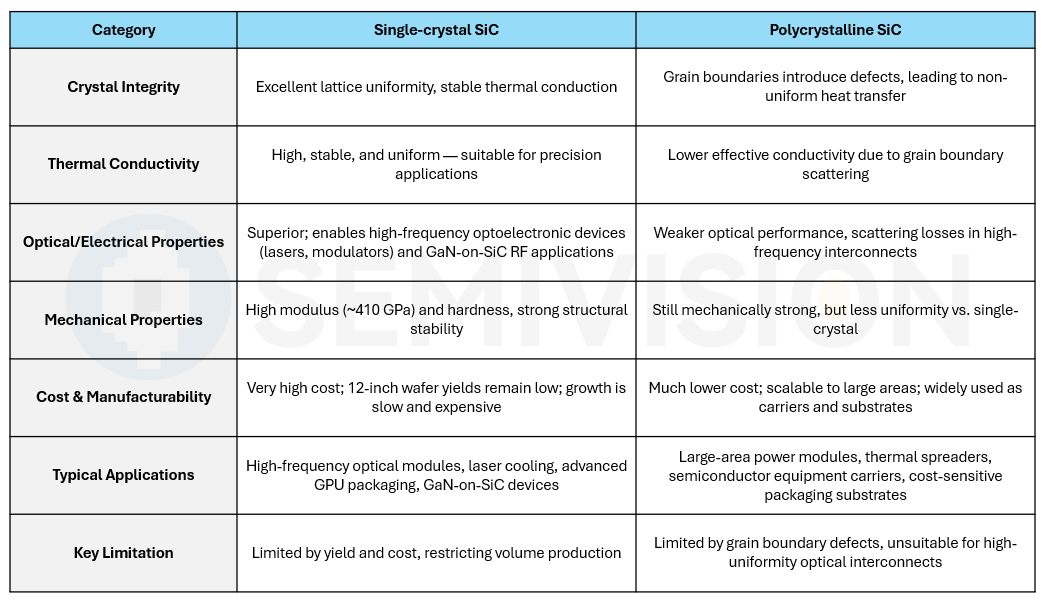
Thetrade-off between performance and cost:
Single-crystal SiC= high performance, low yield, high cost.
Polycrystalline SiC= cost-effective, scalable, but limited in optical/electrical uniformity.
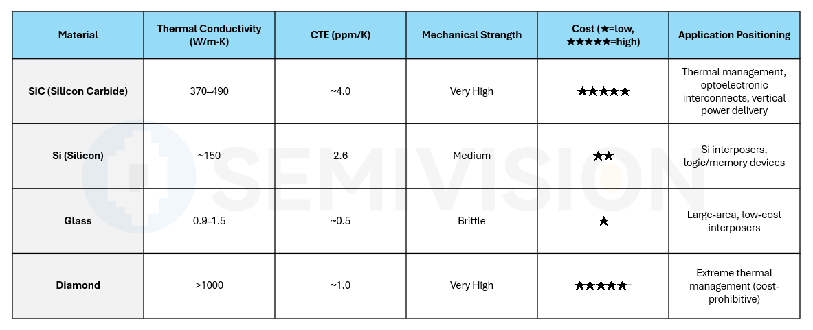
SiCsits uniquely betweendiamond-level thermal/mechanical propertiesandsilicon-like processability, making it the only realistic candidate that can simultaneously supportheat dissipation, structural integrity, and electrical conduction.
Diamondoutperforms in thermal conductivity but is prohibitively expensive.
Glassis cost-efficient but mechanically weak and poor in heat conduction.
Siremains balanced and mature, but limited compared to SiC for extreme thermal and high-power packaging needs.
Core Value of SiC in Packaging Applications
Thermal Substrate
SiC efficiently transfers heat from GPUs/AI ASICs to external cooling systems, addressing the thermal bottlenecks of conventional Si interposers.
Optical Waveguide Interconnects
SiC can be co-integrated with silicon photonics and LN modulators to form a high-speed optoelectronic interconnect platform.
Vertical Power Delivery Integration
Leveraging its wide bandgap (WBG) characteristics, SiC can embed capacitors/inductors to realize HVIC, supporting BSPDN architectures.
Multi-layer Stacking Support
With its high mechanical strength, SiC can sustain large-area packaging of chiplets and HBM stacks.
Technical Challenges
Yield and Cost: 12-inch single-crystal SiC wafers still suffer from high defect density and immature slicing processes.
CTE Mismatch: Differences with HBM and GPU dies require additional buffering designs.
Processing Difficulty: High hardness significantly raises the cost of via drilling and CMP polishing.
Supply Chain Constraints: 12-inch SiC remains in R&D or small-volume pilot production, lacking a fully scaled ecosystem.
SiC combineshigh thermal conductivity, high mechanical strength, and high voltage tolerance, positioning it as a potential “3-in-1 substrate material” for the AI boom—simultaneously solvingthermal management, power delivery, and optoelectronic interconnectchallenges.
However, thecost-performance divide between single-crystal and polycrystalline SiCwill shape near- to mid-term adoption. Compared with silicon and glass, SiC is far more expensive, but itsmarket alignment with AI GPUs/ASICs valued at tens of thousands of dollars eachsupports a rational “high-cost, high-value” trajectory.
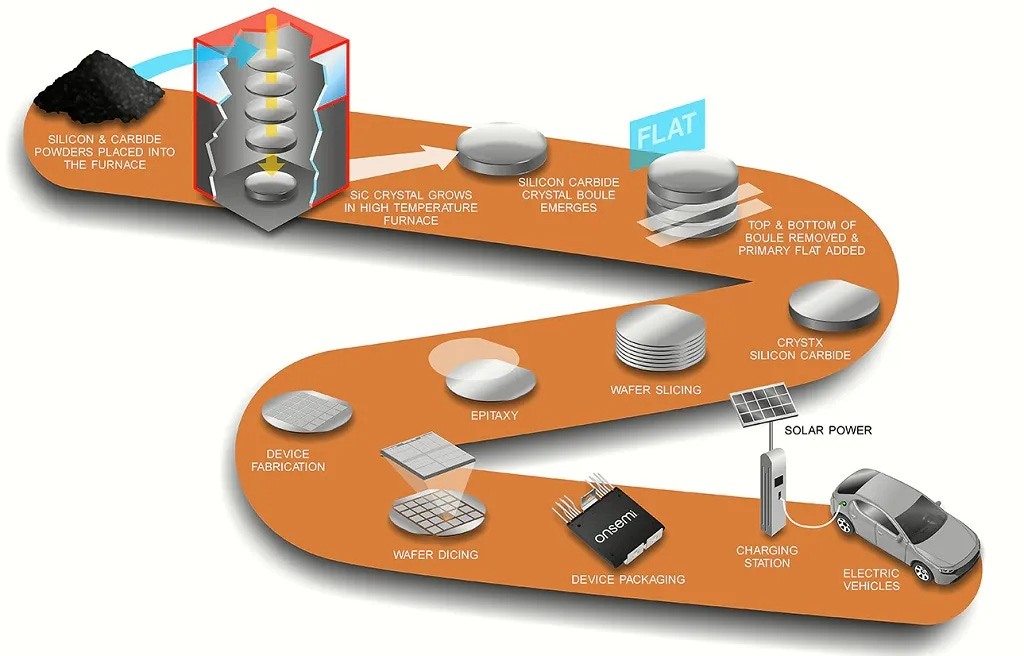
Next Phase: 12-inch SiC Wafer Breakthrough
With breakthroughs in12-inch SiC wafer technology, companies likeTSMCare poised to introduce it into advanced packaging platforms such asCoWoS-Next, SoIC-X, and COUPE. This marks a critical turning point for material applications.
Industry Progress of 12-inch SiC Substrates
As AI megachips continue to scale in both power consumption and die size,traditional 6-inch and 8-inch SiC wafers are no longer sufficientto meet the demands of next-generation packaging and substrates. The emergence of12-inch (300 mm) SiC waferssignals that the materials industry is entering a new era.
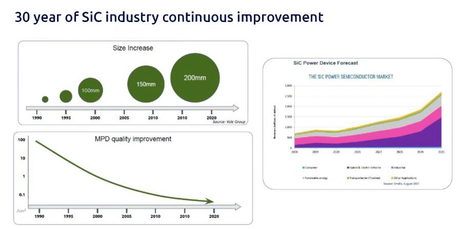
For leading players such asTSMC, Intel, and Samsung, this is not only anevolution of the materials supply chainbut also thefoundation for solving thermal, electrical, and optical challenges in advanced packaging.
Current status: 6-inch wafers dominate today’s commercial market.
8-inch wafersare rapidly expanding, serving as the cost-scaling milestone.
According toMordor Intelligence, 6-inch SiC wafers held about54.4% global market share in 2024. While 8-inch is still emerging, it is forecasted to grow at a29.7% CAGR between 2025–2030.
≥12-inch SiC wafersremain largely in theacademic R&D and prototype stage, highlighting that8-inch will be the key stepping stonebefore full industry migration to 12-inch.
Global SiC Wafer Technology Roadmap
As AI/HPC chip areas and power requirements surge,12-inch (300 mm) SiC wafers have become the focal point of industry attention. Traditional 6-inch and 8-inch formats can no longer support ultra-large interposer and substrate requirements. Reports indicate that:
6-inch SiC: Still mainstream in 2024.
8-inch SiC: Expanding rapidly, already in pilot and early volume adoption.
12-inch SiC: In early R&D, considered thenext critical inflection point.
Leading industry movers include:
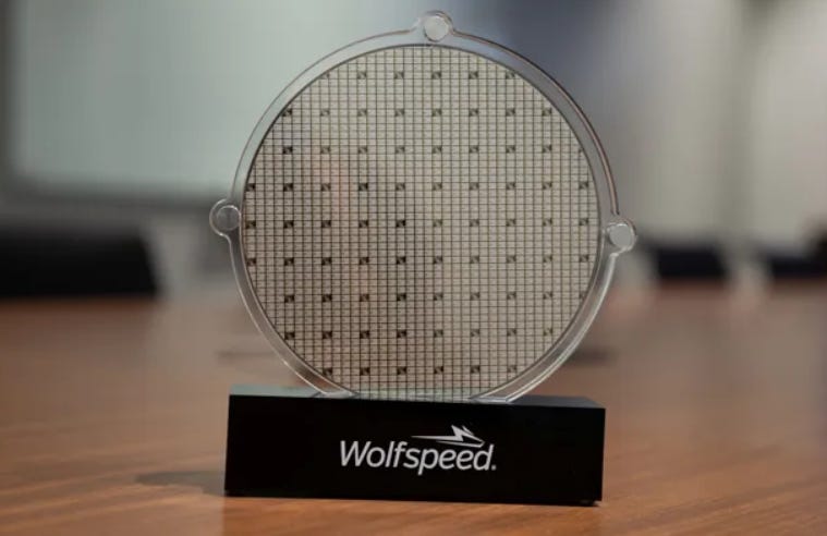
Wolfspeed (U.S.): The world’s largest SiC materials supplier.
ItsMohawk Valley 8-inch fab (New York)began operations in April 2022 and reached20% utilization by June 2024.
The company is now planning a12-inch R&D line at its Palmour facility, with a target ofshipping 12-inch wafers to process fabs by summer 2025.
However, Wolfspeed faces growing competition from therise of Chinese SiC manufacturers.
Wolfspeed’s Business Challenges and the Rise of China’s SiC Industry
News and industry analyses point to multiple factors behindWolfspeed’s current struggles, with therise of Chinese SiC suppliersbeing one of the most critical sources of pressure.
- Rising Cost and Price Competition
Therapid expansion of Chinese SiC substrate and wafer suppliershas increased global supply and intensified competition.
With the maturing of China’s manufacturing ecosystem and falling costs,SiC substrate/wafer prices have shown a sharp downward trend. Some reports indicate thatSiC substrate prices dropped by about 30% in 2024amid China’s capacity expansion.
Wolfspeed, after committing heavy capital investments in8-inch fabs and epitaxy capacity, now bears a heavy cost burden. When orders or selling prices fail to meet expectations,profit margins shrink severely.
- Weaker-than-Expected Demand
Although demand for SiC inAI, EVs, and renewable energyis theoretically growing, several automotive OEMs havedelayed or reduced orders, dragging down Wolfspeed’s sales outlook.
Its aggressive expansion and capital spending have thus become atiming risk.
The company’sstock price collapsereflects investor concerns over its future profitability.
- Heavy Financial Structure and Debt Burden
Wolfspeed carries about$6.5 billion in debt, creating significant pressure from interest payments and capital costs.
With only about$1.3 billion in cash reserves, its ability to cover ongoingcapex and operating costsis constrained.
- Policy, Subsidies, and Market Uncertainty
Wolfspeed has relied in part onU.S. federal or local subsidies. If these incentives fail to materialize as expected, or if policy shifts occur, its financial plans may be disrupted.
By contrast,Chinese policies strongly promote self-sufficiency in SiC, withheavy subsidies and investment flowsinto local companies. While not directly targeted at Wolfspeed, these policies intensify competitive and cost pressures.
Global Competitive Landscape
ROHM / SiCrystal (Japan/Europe): Brought 8-inch production online at a new Japanese fab in 2024, with some capacity shifted to 8-inch by year-end. Collaborates with San’an, and patents suggest a roadmap toward 12-inch.

Chinese players (San’an, SICC):

Scaling both6-inch and 8-inch wafer production, while accelerating12-inch development.
SICClaunched the world’s first12-inch SiC wafer in 2024, expanding in 2025 to covern-type, semi-insulating, and p-type wafers, supported heavily by Chinese government funding.
Soitec (France): ItsSmartSiCtechnology bonds high-quality single-crystal SiC (BPD-free) onto conductive poly-SiC substrates, enabling epi-ready wafers with improved flatness and reduced RDS(on). Currently mass-producing150/200 mm SmartSiCat Bernin 4, with300 mm (12-inch) pilot lines planned. Partners withResonac (Showa Denko)for crystal and epi, while sourcing poly-SiC substrates from Mersen and Tokai Carbon.

Others:Coherent (II-VI), Dow Corning, and Japanese firms like Showa Denkoare pursuing 12-inch SiC projects, focusing on epitaxy and substrate processing as potential critical supply nodes.
Market Status: 8-inch and 12-inch SiC
8-inch SiC wafers: Currently limited global supply, with Wolfspeed as the only short-term high-volume producer. Other vendors are not expected to ramp meaningful capacity untillate 2025 or beyond.
12-inch SiC wafers: Still in early R&D, with production yields and costs yet to stabilize.
TSMC’s Role in 12-inch SiC Adoption
InSeptember 2025, reports indicated TSMC was actively exploring12-inch single-crystal SiC thermal substrateswith equipment makers and compound semiconductor partners.
These wafers demonstratethermal conductivity of 400–500 W/m·K, far exceeding ceramic substrates (200–230 W/m·K) and second only to diamond.
TSMC’s roadmap:
Initial trials withconductive SiCfor thermal substrates.
Later integration ofsemi-insulating SiCforelectro-optical interposers.
Current barrier:wafer slicing still produces wavy surfaces, requiring breakthroughs inyield and cost optimization.

6-inch Era: The Starting Point for Power Electronics
Early SiC applications were primarily focused onEV inverters, high-voltage power modules, and industrial power conversion.
Companies such asWolfspeed, ROHM, and II-VIwere among the first to mass-produce 6-inch single-crystal SiC wafers.
These wafers were sufficient forMOSFETs and Schottky Barrier Diodes (SBDs)but fell short of the needs ofAI/HPC packaging, as theirsize, cost, and yieldcould not support large-area substrates.
8-inch Era: Cost Scaling and Supply Chain Expansion
After 2020,ROHM, San’an, and TYSiC (TianKehanDa)successively entered8-inch wafer production.
8-inch SiC improvedmanufacturing efficiencyand expanded the ecosystem.
However, forlarge-area AI packaging, it remained limited:
Theeffective areawas still insufficient to supportinterposer designs spanning several hundred mm².
12-inch Era: The Inevitable Choice for AI Megachips
The arrival of12-inch SiC wafersoffers AI/HPC vendors the possibility of supportinglarger chiplets, HBM stacks, and photonic modules.
While still in theR&D or small-volume pilot stage, 12-inch has already become afocal point for the semiconductor supply chain.
Yield Challenges and Technical Bottlenecks
Defect Density
Single-crystal growth of SiC remains difficult.
Micropipe defectsand highdislocation densitieson 12-inch wafers continue to be a major issue.
This directly leads tolow yields, making it difficult to sustain large-scale production.
Processing Difficulty
With hardness approaching that of diamond, SiC isextremely costly to processin slicing, CMP polishing, and via drilling.
For AI packaging, which requireshigh-density TSVs and thermal vias, this is a significant challenge.
Thermal Expansion Mismatch
SiC’sCTE (~4 ppm/K)differs from silicon (2.6 ppm/K), glass (0.5 ppm/K), and copper (16 ppm/K).
When integrated withGPU dies or HBM stacks, additionalbuffer layers, underfill materials, or hybrid bondingare required to relieve stress.
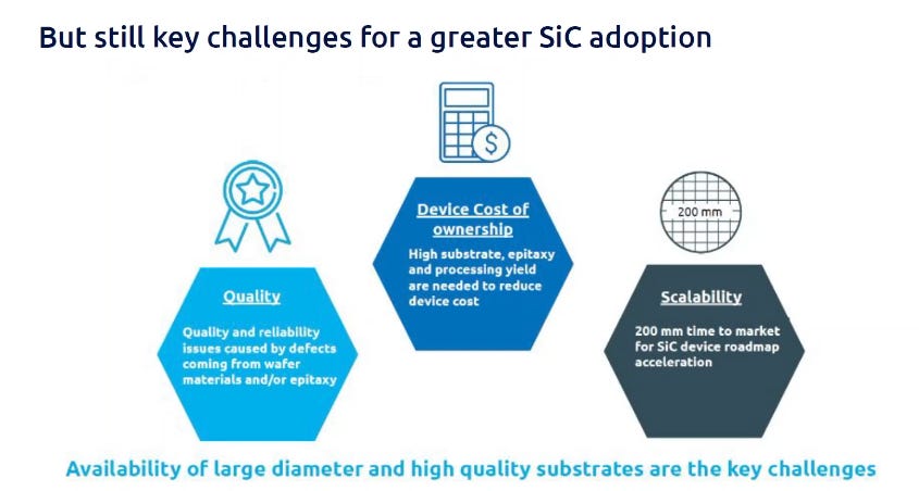
Market Size Forecast
The globalSiC wafer marketis projected to reach$970 million in 2025and expand to$2.65 billion by 2030, representing a22.24% CAGR. Growth drivers include the adoption of800 V EV platforms, industrial power supply, high-frequency communications, and government subsidies.
As shown in forecasts, the market will growmultiplicatively between 2025–2030.
6-inch waferswill remain dominant.
8-inch wafersare expected to attract more investment as capacity expands and yields improve.
12-inch wafersare not yet in mass production but ongoingR&D by academia and industry is paving the way.
Capacity Bottlenecks and Investment Outlook
Capacity Constraints
Global12-inch SiC wafer productionremains limited to small-scale R&D.
Wolfspeed, ROHM, and Chinese supplierswill continue to focus mainly on8-inch wafers through 2026–2027.
Investment Trends
TheU.S. and Japanese governmentsare actively subsidizing SiC production lines to ensuresupply chain securityin the EV and HPC era.
Chinais accelerating self-sufficiency, with plans to achieve12-inch SiC mass production by 2027.
Implications for the AI Industry
If12-inch SiC wafer capacityfails to scale on time, it may become abottleneck for HPC and AI packaging.
TSMC, Intel, and other packaging leadersmay need to secure long-term supplier agreements or evendirectly investin SiC suppliers to ensure reliable supply.
The12-inch SiC substrateis at aturning point from R&D to industrialization. While yield and processing costs remain bottlenecks, the value ofAI megachip applications makes its economics justifiable.
Key suppliers(Wolfspeed, ROHM, San’an, TYSiC, etc.) are accelerating investments, supported byU.S., Japanese, and Chinese policies.
ForTSMC, the12-inch SiC waferis not just a new material—it is thefoundationfor ensuring thatCoWoS-Next and COUPE platformsmaintain leadership in the AI era.
Whoever achieves12-inch SiC mass production firstwill secure an edge across thethree battlefronts of thermal management, power delivery, and optical interconnects.
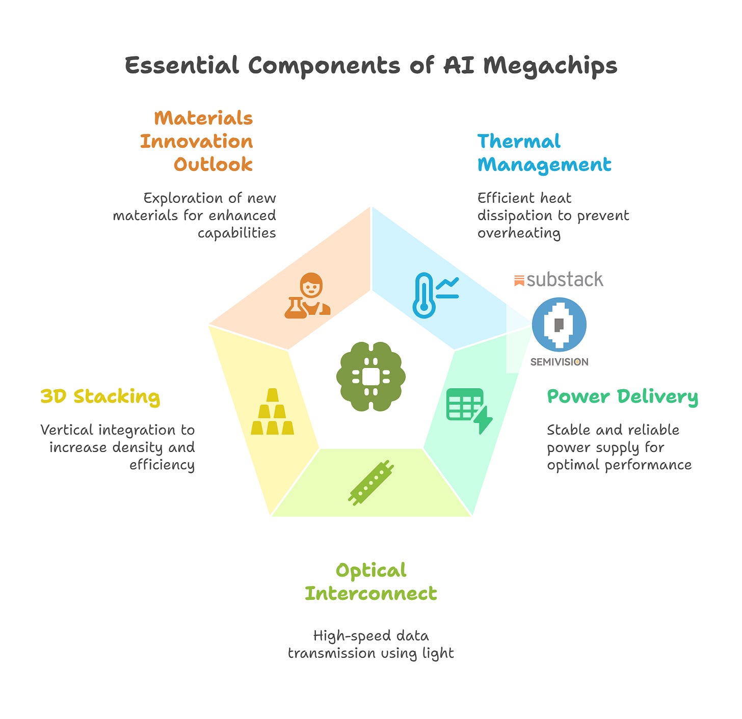
Core Requirements of AI Megachips: Thermal, Power, Optical, and 3D Integration
Driven byGenerative AI and High-Performance Computing (HPC), single-chip design and manufacturing are pushing beyond historical limits. For example, NVIDIA’sGB200 and GB300 GPUsnow approach or even exceed1 kW per chip, with package size and interconnect complexity far surpassing conventional logic devices.
In this environment, designers of AI megachips must confrontfour fundamental challenges—thermal management, power delivery, optical interconnect, and 3D stacking. These are not only decisive factors for system performance, but also key criteria inmaterials selection.
Modern AI/HPC chips now exceed800–1000 mm² in area, with power consumption in thehundreds of watts to kilowatt-class, placing unprecedented demands on substrate materials.
- Thermal Management
At such high power densities, traditionalsilicon interposers(~150 W/m·K thermal conductivity) cannot dissipate heat effectively. If heat is not removed rapidly, chips faceperformance degradation, reduced lifetime, and severe bandwidth loss in optoelectronic devices.
AI packaging must handle bothinternal cooling(GPU + HBM stacks) andexternal cooling(liquid cold plates, immersion systems), while keeping optical modules (lasers, modulators, etc.) within±0.1 °C stability.
SiC, withthermal conductivity of 400–500 W/m·K(approaching copper levels), serves as anexcellent thermal substrate, capable of rapidly channeling heat to external systems while stabilizing optoelectronic device temperatures.
- Power Delivery
Power currents for megachips can exceed1,000 A. Traditional PCB/ABF substrates introducelong current paths, leading toIR drop and transient voltage noise.
Solutions includeBackside Power Delivery Networks (BSPDN), which move power planes to the wafer backside, reducing path length and improving integrity.
Future designs will integrateembedded decoupling capacitors (e.g., 3D deep trench capacitors, DTCs)and inductors directly within the substrate, enabling a “complete power delivery ecosystem” at the package level.
With itswide bandgap and high breakdown field,SiC is suitable for HVIC (High-Voltage IC) substrates, allowing embedded capacitors/inductors to supportmulti-layer BSPDN, enabling shorter and more efficient power delivery.
- Optical Interconnect
As AI clusters scale tohundreds of GPUs, traditional high-speed copper SerDes (112G/224G) face physical limits, withlatency and power skyrocketing.
Optical interconnects—Co-Packaged Optics (CPO)andOptical I/O (OIO)—are emerging as the shared direction for NVIDIA, Intel, and Broadcom.
Key requirements includelaser temperature stability, high-bandwidth modulators, low-loss waveguides, and seamless substrate integration.
Role of SiC:
Withhigh resistivity and low dielectric constant, SiC enableslow-loss high-speed signal transmission.
Itshigh thermal conductivitysupports TFLN (LiNbO₃) modulators to maintain>140 GHz bandwidthunder high power.
As anoptical interposer material, SiC can host bothsilicon photonics and LN modulators, shortening optical paths between sources and receivers.
At multi-Tb/s bandwidths, copper wiring becomes prohibitively inefficient.CPO modulesplace optical devices within the 3D package, connecting fibers directly to switches/GPUs.
By reducing DSP count and electro-optical conversion steps, interconnect energy can drop below1 pJ/bit.
Studies show Broadcom and Cisco’s early CPO designs save30–50% power, while Ayar Labs demonstrated16 Tbps at <5 pJ/bit.
The challenge: photonic circuits inside packages introducethermal coupling—heat alters optical paths, while silicon-based cooling shiftslaser wavelengths. Thus,materials with high thermal conductivity and electrical insulation, like SiC, are essential for optical interposers.
- 3D Stacking
AI GPUs typically stack6–12 HBM chipstightly with the logic die, forming advanced2.5D/3D packages.
This demands substrates with sufficientarea, thickness, and mechanical strength.
Large-area stacks suffer fromwarpage, while ABF lacks sufficient rigidity and silicon interposers are expensive and size-limited.
SiC, with aYoung’s modulus ~410 GPaand extreme hardness, can withstand large chiplet + HBM stacks. Combined with3D hybrid bonding, SiC substrates provide bothmechanical support and thermal dissipation.
Thus, integrating SiC into unified chip packages addresses bothstructural reliability and thermal challengesfor large-scale stacking.
- Materials Innovation Outlook
Traditionalcopper and tungsten interconnectsface scaling bottlenecks (resistivity increase, electromigration). The industry is exploringmolybdenum (Mo)for its lower resistivity and higher thermal stability to improve PDN performance.
In packaging,backside power deliveryvia through-silicon backside vias is under study. However,removing silicon heat spreaders introduces new thermal challenges, reinforcing the need for materials like SiC to balancepower and heat management.
TSMC Advanced Packaging Platforms and SiC Alignment
TSMC’sCoWoS® (Chip-on-Wafer-on-Substrate)employssilicon interposersto enable 2.5D high-bandwidth integration, whileSoIC® (System on Integrated Chips)leveragesTSVs and hybrid bondingfor vertical stacking, improving interconnect density and reducing wiring length. As chip density increases, thermal management becomes a critical challenge. ExploringSiC thermal substratesoffers a pathway to enhanced cooling.

TSMC has been investigating the use ofconductive SiC as a thermal substrate, with a roadmap to adoptsemi-insulating SiC as an interposerin the future. If manufacturing and cost barriers can be overcome, SiC could replace portions of silicon or ceramic inCoWoS/SoIC interposers and base layers.
Integration Potential Across TSMC’s Platforms
CoWoS® (Chip-on-Wafer-on-Substrate)
2.5D packaging connects large GPUs and HBM via silicon interposers.
InCoWoS-Next, SiC could replace silicon/ceramic as the interposer, withsuperior thermal conductivityovercoming silicon’s thermal bottleneck.
SiC layers could also integratepassive components (inductors, capacitors)via stacking, improvingpower delivery networks (PDN)efficiency.
SoIC® (System on Integrated Chips)
TSMC’s 3D vertical stacking platform, covering both multi-die and heterogeneous integration.
COUPE (CoMPact Universal Photonic Engine)is built on SoIC, using hybrid bonding to directly stackEIC (electronic ICs)withPIC (photonic ICs).
In SoIC-X or future variants, SiC could serve as ahigh-voltage, high-thermal-conductivity support layer, enablingbackside power delivery networks (BSPDN)and embedding3D inductors/capacitorsfor complete on-die/on-package power systems.
COUPE® (Compact Universal Photonic Engine)

TSMC’s next-gen co-packaged optics platform, designed for ultra-high-bandwidth optical interconnect.
Based on SoIC, COUPE integratesmodulators, fibers, and ASICsviaCu-Cu and hybrid bonding.
SiC could serve as theoptical interposer material:
Semi-insulating SiCprovides a stable optical waveguide platform, dissipates heat rapidly, and reduces photonic device thermal drift.
Conductive SiCcan be used as integratedpower/ground layers.
This would extend thetechnical lifetimeof TSMC’s CoWoS, SoIC, and COUPE platforms, ensuring they meet thethermal, electrical, and optical demandsof AI packaging.
However, as of today,COUPE still relies on CoWoS as its key base, with SiC integration remaining at theR&D stage.
Competitive Strategies: Intel vs. Samsung
Intel
Actively advancingmulti-layer advanced packaging, includingFoverosandEMIB, and was an early mover inco-packaged optics (CPO).
In 2024, Intel showcased its firstOptical Compute Interconnect (OCI) chiplet system, a co-packaged optical I/O chip enabling64 channels × 32 Gbps bidirectional optical transmissionwithin CPU/GPU systems.
This approach, leveraging on-die photonic links, significantly enhancesbandwidth and energy efficiency, positioning OCI as a critical technology forAI cluster scaling.
However, Intel hasnot announced plans to adopt SiC substrates, continuing to rely mainly onsilicon and alternative dielectrics.

2025年6月3日
Samsung
Pursuing a different path in interconnect materials.
Reports in 2025 indicated that Samsung plans toadopt glass interposer layers for AI chip 2.5D packaging by 2028.
Glass offershigher dimensional stability, precision, and lower costcompared with silicon interposers, improving bothAI GPU/ASIC packaging performance and production efficiency.
This strategy highlights Samsung’s focus oncost reduction and interconnect stability, and a decisionnot to pursue SiC adoptionin the near term.
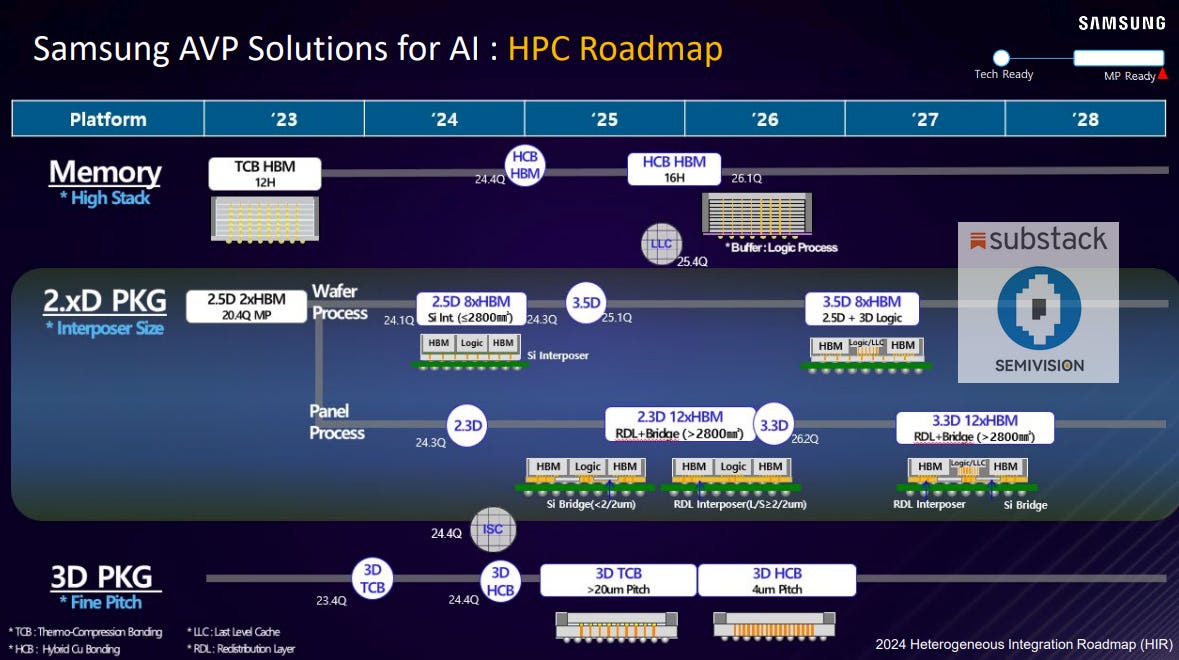
Overall Comparison
Intel: Focused onoptical interconnect leadership(OCI, CPO), enhancing bandwidth and efficiency for AI systems.
Samsung: Focused onglass interposers and panel-level packagingfor cost-efficient scaling of AI chips.
Both remain anchored insilicon, glass, and copper-based solutionsfor advanced packaging in the near term.
By contrast,TSMC and select high-end applications (e.g., NVIDIA)are exploringSiC as a differentiated enablerin the domains ofthermal, power, and optical integration.
Challenges of 12-inch SiC: Yield, Cost, and CTE Mismatch

While the value of 12-inch SiC is undeniable, its industrialization still faces multiple bottlenecks:
- Crystal Defects and Yield
Growing single-crystal SiC is extremely challenging.Micropipe defectsand highdislocation densityremain significant issues at 12-inch wafer size, with yields still low even at 150 mm.
These defects directly reduce product yield, posing a major barrier forhigh-reliability AI packaging applications.
Growth requires ultra-high temperatures and costly consumables (graphite, SiC furnace cores). SiC is brittle and hard to cut, further lowering yield and raising costs.
Entegris has noted that due to high equipment and consumable costs,SiC devices can cost up to 8× more than silicon devices.
In 8-inch production, SiC yields are15–20% lower than 6-inch, though improvements in hot-zone design and defect analysis are narrowing the gap.
Consumables such as graphite components must be replaced after only a few cycles, and contamination can scrap entire wafers.
- Processing Difficulty and Cost
SiC’s hardness approaches diamond. Growth is slow (a 4–6 inch boule yields only 15–20 wafers).
Etching, CMP polishing, and via drillingare time- and energy-intensive, raising costs far above silicon or glass.
High hardness makes TSV/thermal via formation for advanced packaging especially challenging.
Producing 12-inch SiC requires new equipment designs.
For example, a200 mm SiC growth furnace costs $15–20 million, versus$8–12 million for 150 mm, with 8-inch wafers offering ~2.2× chip output.
Yet 12-inch wafers often sufferwavy surface morphology, demanding new slicing, grinding, bonding adhesives, and packaging techniques to improve flatness and yield.
- Coefficient of Thermal Expansion (CTE) Mismatch
SiC’s CTE is~4.0 ppm/K, compared to~2.6 for silicon,<1 for glass, and~16 for copper.
In heterogeneous packaging (chiplet + HBM), these mismatches inducewarpage and stress accumulation.
Solutions includebuffer layers, invar structures, or void-free underfillto mitigate stress.
Organic interposers have high CTE but are low-cost and mature.
Glass interposers, withCTE of 3–4 ppm/°C, fall between silicon and organics, reducing warpage and offering30–40% cost savings, with current yields at~80–85%and expected improvement.
TSMC is exploring hybrid SiC + glass use—deploying SiC incritical thermal zones, while using glass or organic substrates in large-area interconnects to balancethermal performance and cost.
- Capacity and Economics
Global 12-inch SiC remains in small-scale R&D, with no true mass-production capacity yet.
Despite its high price, SiC is economically feasible inAI GPUs/ASICs costing tens of thousands of dollars each, where customers tolerate higher material costs.
However, without improved yields and expanded capacity,AI packaging adoption will be constrained.
Industry consensus: for leaders likeTSMC,stable supply and yield matter more than material cost.
If 12-inch SiC capacity remains insufficient, foundry leaders may be forced tolock in suppliers or co-invest directlyto secure demand.
Future Market Scale and Strategic Implications
TheSiC wafer marketis projected to grow at a22.24% CAGR between 2025 and 2030.
Asiais the largest market, accounting for~63.4% of revenue in 2024, driven by vertically integrated strategies that attract investment across the value chain.
Chinese firms(e.g., San’an Optoelectronics) are building fully integrated production lines to reduce costs, whileU.S. and European playersfocus ondefect density reduction and long-term supply agreements.
Ultimately, the SiC market must balancecost, yield, and performance.
8-inch mass productionwill be the critical inflection point, while12-inch adoptiondepends on process maturity.
Growth Drivers and Regional Initiatives
TheSiC substrate marketis entering a high-growth phase, expected to beseveral times larger by 2030than it is today. The main growth drivers are:
EVs and high-voltage power devices (6–8 inch wafers)
AI/HPC packaging (8–12 inch wafers)
Government support is also accelerating adoption:
United States: CHIPS Act funding supports SiC production.
Japan & U.S.: Subsidies for SiC materials and equipment.
China: Promotes self-sufficiency, with plans to achieve12-inch SiC mass production by 2027.
Strategic Implications for AI Packaging
If12-inch SiC capacitylags, it may become abottleneck for AI packaging.
Whoever achieves high-yield 12-inch SiC mass production firstwill gain a decisive edge inthermal management, power delivery, and optical interconnect.
ForTSMC, adopting SiC substrates is not only about extending the lifecycle ofCoWoS, SoIC, and COUPE platforms, but also aboutsecuring leadership in the next wave of AI packaging competition.
The critical next step lies in overcoming theyield and capacity challengesof 12-inch SiC, alongside building a resilientsupply chain ecosystem.
Strategic Implications for TSMC
ThroughCoWoS®, SoIC®, and COUPE®, TSMC has built a comprehensiveheterogeneous integration platform. The introduction ofSiC as a thermal substrate or as an optical/electrical interposerwould further reinforce its leadership in AI and high-performance computing (HPC) packaging. Advancing12-inch SiC technologyoffers several strategic advantages:
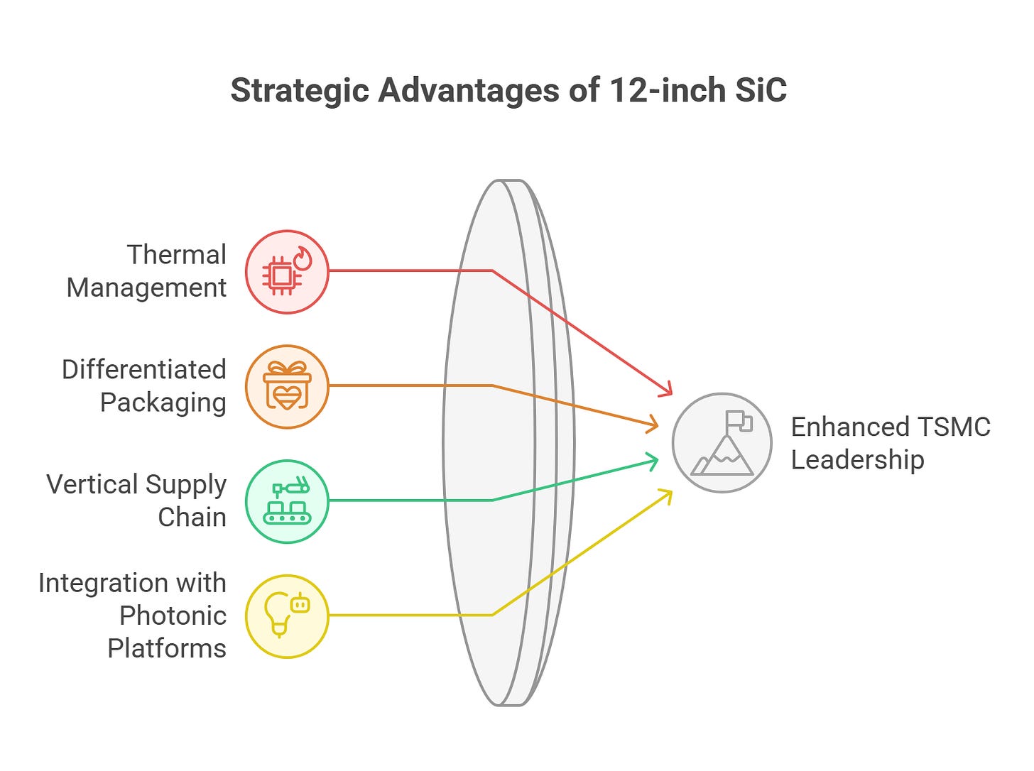
Thermal Management and Performance Gains
SiC’s high thermal conductivity enables efficient heat dissipation from AI chips, reducing temperature gradients and increasing both frequency and power limits.
Differentiated Packaging Capability
In an era where customers focus on power and bandwidth, offering SiC substrates can create competitive barriers, differentiating TSMC fromIntel and Samsung, which emphasize glass-based solutions.
Vertical Supply Chain Control
By collaborating with suppliers such asSoitecto develop 12-inch SiC, TSMC can secure material sources and strengthen bargaining power, while also expanding partnerships withpower semiconductor companies(e.g., automotive chipmakers).
Integration with Photonic Platforms
TheCOUPE platformrequires a high-thermal-conductivity, insulating optical interposer. Semi-insulating SiC wafers are promising candidates. Combined withSoIC and CoWoS, TSMC could deliver acomplete optoelectronic heterogeneous integration solution.
Risks and Challenges
Entering SiC packaging requiressubstantial equipment and R&D investment, while12-inch yield rates remain uncertain. Any delay in mass production could impact customer adoption timelines.
Theglobal wafer supply chainis reshaping. Chinese players are leveragingpricing strategies to drive down SiC costs. If prices fall sharply, TSMC may needlong-term contracts with customersto share risks and ensure return on investment.
Strategic Outlook
With itshigh thermal conductivity, wide bandgap, and high breakdown field, SiC is evolving from power semiconductors intoadvanced packaging materials. TSMC is actively exploring SiC’s potential as athermal substrate, optical interposer, electrical interposer, and vertical power delivery substrate, enabling AI chips to achievehigher power density, better heat dissipation, and faster optical interconnects.
Although12-inch SiC yield, cost, and CTE mismatchremain significant barriers, progress is being made:
SICCintroduced the first 12-inch SiC wafer.
Soitec’s SmartSiChas entered mass production, addressing defect and cost challenges.
Meanwhile, international competitors such asIntel and Samsungare pivoting towardglass interposers, showing that material choices remain diverse. Yet, SiC’ssuperior heat dissipation and high-voltage endurancestand out as unique strengths.
Driven byAI and EV markets, the globalSiC wafer market is expected to grow to $2.65 billion by 2030. If TSMC can securematerials and packaging technology leadership, it will maintain itscompetitive edge in the next wave of semiconductor competition.
Key Challenges in AI Megachip Packaging and the Role of SiC
Power Delivery Challenge: BSPDN and PDN Voltage Drop
AsAI GPUs and custom ASICsscale larger, the current demand per chip can exceed1,000 A. Traditional power delivery throughPCBs or ABF substratessuffers from excessively long power paths and large parasitic inductance, causingIR dropandtransient voltage droop—now critical bottlenecks forPower Integrity (PI).
To address PDN voltage drop issues, the industry is advancingBackside Power Delivery Networks (BSPDN):
Intelhas introducedPowerVia, delivering power directly through backside metal layers to shorten transmission distance.
TSMCis exploring the combination ofSoIC + BSPDN, further reducing voltage fluctuations and improving both efficiency and stability.
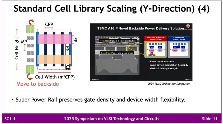

2025年6月13日
Looking ahead,AI GPUs/ASICswill need to integratedeep trench capacitors (DTCs), inductors, and other passive devicesdirectly into the package or substrate, reducing reliance on external power delivery.
This is whereSiCcan play a pivotal role:
With itshigh breakdown fieldandwide bandgap properties, SiC can serve as the substrate forHigh-Voltage Integrated Circuits (HVICs).
This enables support foron-chip power architectures, reducing transmission losses and delivering higher efficiency in AI megachip packaging.

This shows thatSiC is not just a substitute material, but theonly substrate candidate capable of simultaneously addressing all four challenges—thermal, electrical, optical, and mechanical—in AI megachip packaging.
TSiCV (Through-SiC Via) Technology and Highlights from Three Papers
- Background: 3D Interconnect and Vertical Via Technologies
To meet the demands ofhigh-performance computing, artificial intelligence (AI), and communications systemsfor high frequency, wide bandwidth, and low power consumption, semiconductor packaging has evolved from traditional2D IC integrationtoward2.5D/3D heterogeneous integration.
3D packaging enables vertical signal and power transmission by formingthrough-viaswithin the substrate. Common via technologies include:
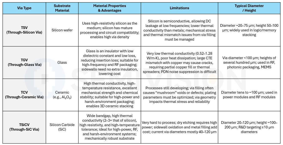
Summary of Three Research Papers on TSiCV Technology: Electrical Properties, Fabrication Processes, and Optimization Methods, with Comparisons to TSV/TGV/TCV and Potential Applications in AI Co-Packaged Optics (CPO) and Photonics
Paper 1:RF Modelling of Through-SiC Vias and Fabrication of SiC-based Interposer
- Research Objective and Background
Through-SiC via (TSiCV) structures take the form ofmetal–insulator–semiconductorsystems, with RF performance strongly dependent onsubstrate resistivity, dielectric constant, insulation thickness, and geometric dimensions.
The authors extended aTSV-based analytical modelto simulate and measure TSiCVs inhigh-resistivity (≥10⁶ Ω·cm)andlow-resistivity (0.02 Ω·cm)SiC substrates.
Since SiC’s dielectric constant (~9.66) is lower than silicon’s (~11.9), TSiCVs exhibitlower capacitance at the same dimensions, which benefitsinsertion loss reduction.
- Geometry and Material Properties
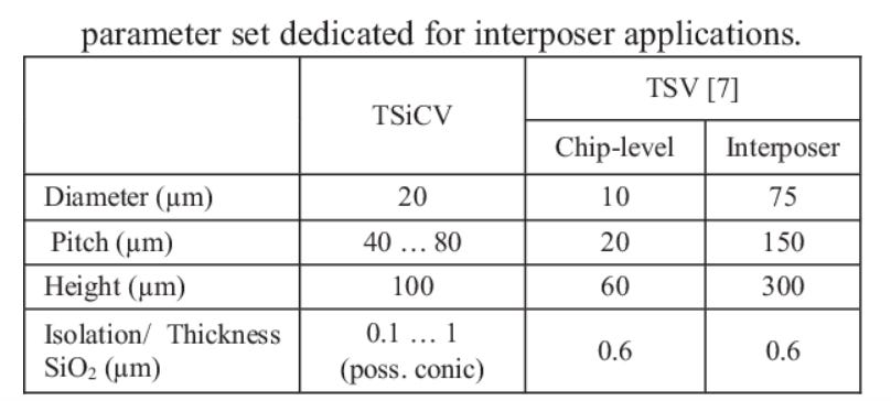
TSiCVs: ~20 µm diameter, 40–80 µm pitch, 100 µm depth, insulation thickness 0.1–1 µm.
Conventional TSVs: ~75 µm diameter, 150 µm pitch.
Thesmaller size and higher thermal conductivity of SiCmake it more suitable forhigh-density advanced packaging.
- Electrical Modeling and Results
Anequivalent circuit modelwas built using series R/L and parallel C/G elements to analyze the effects of insulation thickness and via pitch oncharacteristic frequency and insertion loss.
Example: For 20 µm diameter vias at 40 µm pitch with 0.1 µm insulation thickness, the characteristic frequency was ~34 GHz.
High-resistivity SiCbehaves nearly like an insulator, with negligible carrier loss.
Low-resistivity SiCinducesslow-wave modes, reducing phase velocity and significantly increasing insertion loss.
Using aconical oxide layer(thicker insulation near the top) reduces electric field concentration and lowers insertion loss.
- Conclusion
For RF applications,high-resistivity TSiCVsdemonstrate transmission performance comparable to, or even better than, silicon TSVs.
With optimized via pitch and insulation thickness,insertion loss can be kept below 0.5 dB/10 mm.
This study establishes a theoretical foundation for applying SiC packaging inmmWave and high-frequency communications.
Paper 2:TSiCV-Based Silicon Carbide Interposer Technology
- Fabrication Process
Process integration:
Since SiC front-end processing requireshigh-temperature annealing at 1600–2100 °C, the conventionalvia-firstapproach used in silicon cannot be applied. Instead, the study adoptedvia-middleorvia-lastintegration flows. For passive interposer boards (without active devices), vias can be directly etched into unfinished SiC substrates.
Via etching:
High-hardness SiC was etched usinghigh-power reactive ion etching (RIE)withSF₆/O₂/He gases. Coil power and platen power were found to be the dominant factors affecting etch rate. In experiments, vias with40–120 µm diametersachieved etch rates of1.1–2.0 µm/min. Mask selectivity improved with larger via sizes: ~21:1 for 40 µm vias, and ~31:1 for 120 µm vias.
Via insulation:
Forsmall, high-aspect-ratio TSiCVs, inorganic PECVD layers ofSiO₂/Si₃N₄were used.
Forlarger diameters (≥80 µm), organicpolyimide or BCB polymerfilling was adopted. BCB was vacuum-compressed to fully fill the via, followed by re-opening using an excimer laser.
Breakdown strength:BCB ~5.1 MV/cm, inorganic oxide layers~4–7 MV/cm.
Metallization & backside processing:
After depositing aTi/Cu seed layeron the insulation, vias were filled via electroplating. Backside grinding and CMP or dry etching were performed to expose the vias. Finally,redistribution layers (RDLs)andsolder bumpswere formed.
- Performance and Applications
The study demonstrated40–120 µm viasfabricated in200 µm-thick SiC substrates, meeting bothcurrent-carryingandthermal dissipationrequirements forhigh-power modules.
Owing to SiC’shigh thermal conductivity and mechanical strength, these interposers are applicable toautomotive electronics, high-temperature sensors, and RF data converters.
The process flow issimilar to silicon TSV, but sinceSiC etching is largely physical, it requireshigher equipment capability and substrate flatness.
Future targets includescaling via diameters down to ~10 µm, enablinghigher-density 3D integration.
Paper 3:Investigation and Modeling of Etching Through Silicon Carbide Vias (TSiCV) for SiC Interposer and Deep SiC Etching for Harsh Environment MEMS by DoE
- Design and Experiment (DoE)
The study conducted29 Design of Experiment (DoE) runsto evaluate the impact of RIE parameters onetch rateandsidewall angle.
Results showed thatcoil power was the most critical factor:
For an80 µm via, increasing coil power from 1000 W to 2000 W improved the etch rate from~1.42 µm/min to 1.81 µm/min.
A120 µm viaachieved up to2.0 µm/minunder optimized conditions.
As via density increased, etch rates decreased due tolimited plasma distribution.
Helium (He) flowreducedmicro-trenching effects, whileplaten powerincreased etch rate but lowered mask selectivity.
- Insulation and Metallization
The paper comparedcross-sections of PECVD SiO₂ vs. BCB-filled TSiCVs:
BCBcould achieve filling thicknesses >8 µm, making it suitable forlarge-diameter vias.
PECVD oxide layerswere thinner, better suited forsmall-diameter vias.
FollowingTi/Cu seed layer deposition, copper electroplating was performed, wafers were thinned, andRDLs were fabricated.
AMEMS pressure sensorwas integrated on a SiC interposer for testing:
Series resistance increased by only~1 Ω.
Output bias shift was<0.5 mV, demonstrating minimal parasitic impact.
- Conclusion
The DoE-derived model provided predictive insights into theetching process, showing etch rates ofup to 2 µm/minunder optimized parameters, and up to3–4 µm/minwhen coil power exceeded the tested DoE range.
By integratingRIE etching, polymer/oxide insulation, electroplating, and backside processing, the study proved thatSiC interposers can support 3D integration in harsh-environment MEMS, offering bothhigh reliability and excellent thermal performance.
Comparison of TSiCV with TSV, TGV, and TCV
Electrical Performance and Thermal Management
Dielectric properties:
The dielectric constant of SiC (~9.66) is slightly higher than glass but lower than silicon. Combined with high-resistivity substrates, TSiCVs can effectively reduce via capacitance and transmission loss. On high-resistivity SiC, TSiCV insertion loss and phase velocity approach ideal levels. In contrast, silicon TSVs—due to substrate conductivity—are prone to slow-wave modes, requiring high-resistivity silicon and thick insulation to mitigate loss.
Thermal conductivity and heat dissipation:
SiC has2–3× higher thermal conductivitythan silicon, enabling TSiCVs to carry larger currents and handle higher heat loads. Glass TGVs, with extremely low thermal conductivity, require copper pillar arrays or thermal spreaders for high-power applications. Ceramic TCVs exhibit both high thermal conductivity and temperature tolerance, making them well-suited for power modules.
Mechanical reliability:
Both SiC and ceramics offer high hardness and thermal stability, resistant to high temperature and corrosion. Glass TGVs, however, are prone to radial cracking due to CTE mismatch with copper and require careful thermal ramp rates (<6.5 °C/min) to avoid fracture.
High-frequency applications:
TGVs, being insulating with low dielectric loss, are excellent for mmWave and RF communications, though PDN noise suppression is challenging without ground vias or EBG structures. TSiCVs on high-resistivity SiC also enablelow-loss, high-frequency transmission, while offering better thermal performance than TGVs, making them suitable for applications requiring bothheat dissipation and RF performance.

Potential Applications of SiC in Co-Packaged Optics (CPO)
CPO Demands and Technical Challenges
With the exponential growth ofAI model scaleanddatacenter traffic,Co-Packaged Optics (CPO)has emerged as a key solution by integratingelectronic ICs (EICs)andphotonic ICs (PICs)within the same package. By replacing copper interconnects with optical fibers, CPO dramatically increasesbandwidth densitywhile reducingpower consumption and latency.
International initiatives such asDARPAandPhotonixFABare actively advancing this trend. According to ASE, vertical interconnects in photonic systems are typically achieved usingsilicon TSVs or tall copper pillarsto stack PICs with EICs. However, CPO packaging involves multiple elements—lasers, optical interfaces, fiber arrays—making assembly highly complex and imposingstringent thermal management and power integrity requirements.
Why Introduce SiC Interposers?
Thermal bottlenecks and power demand
As AI GPU power continues to rise, conventional silicon interposers struggle with thermal resistance. Reports indicate thatSiC substrates are being explored to overcome this limitation.
Media sources suggest thatNVIDIA plans to replace silicon interposers with SiC in CoWoS packaging, whileTSMC has engaged multiple partners to co-develop SiC interposer technology.
With2–3× the thermal conductivity of silicon, SiC can lower GPU junction temperatures by20–30 °Cand reduce thermal resistance by nearly70%.
Moreover,12-inch SiC substratesoffer ~90% more area than 8-inch, enabling integration of more chiplets to support7× reticle-size CoWoS packages.
Power delivery efficiency
Reports note that SiC interposers can supportsmaller, more efficient voltage regulation modules, shortening PDN paths and improving power integrity—aligning well with the needs of high-power AI chips.
High-frequency and photonic interconnects
SiC’shigh-resistivity substratesandlow dielectric constantenablelow-loss, high-speed transmissionwithin the package.
Itsmechanical hardnessandthermal stabilityallow it to withstand the heat load of photonic laser modules and support MEMS optical devices.
Studies further show thathigh-resistivity TSiCVs maintain low insertion loss and fast phase velocity across 0–100 GHz, which is critical for future optical and mmWave interconnects.
Industry trends and challenges
Supply-chain reports suggest atransition phase: silicon interposers will remain in use forRubin GPUs (2025–2026), withSiC interposers introduced from 2027 onward.
Barriers include SiC’sdiamond-like hardness, which makes processing extremely difficult and costly (requiring high-power RIE and specialized grinding).
However, as volumes increase and technology matures, costs are expected to decline.
Role and Outlook of SiC in CPO Packaging
Thermal management and system reliability
CPO packages combine AI processors and photonic engines, both of which generate substantial heat.
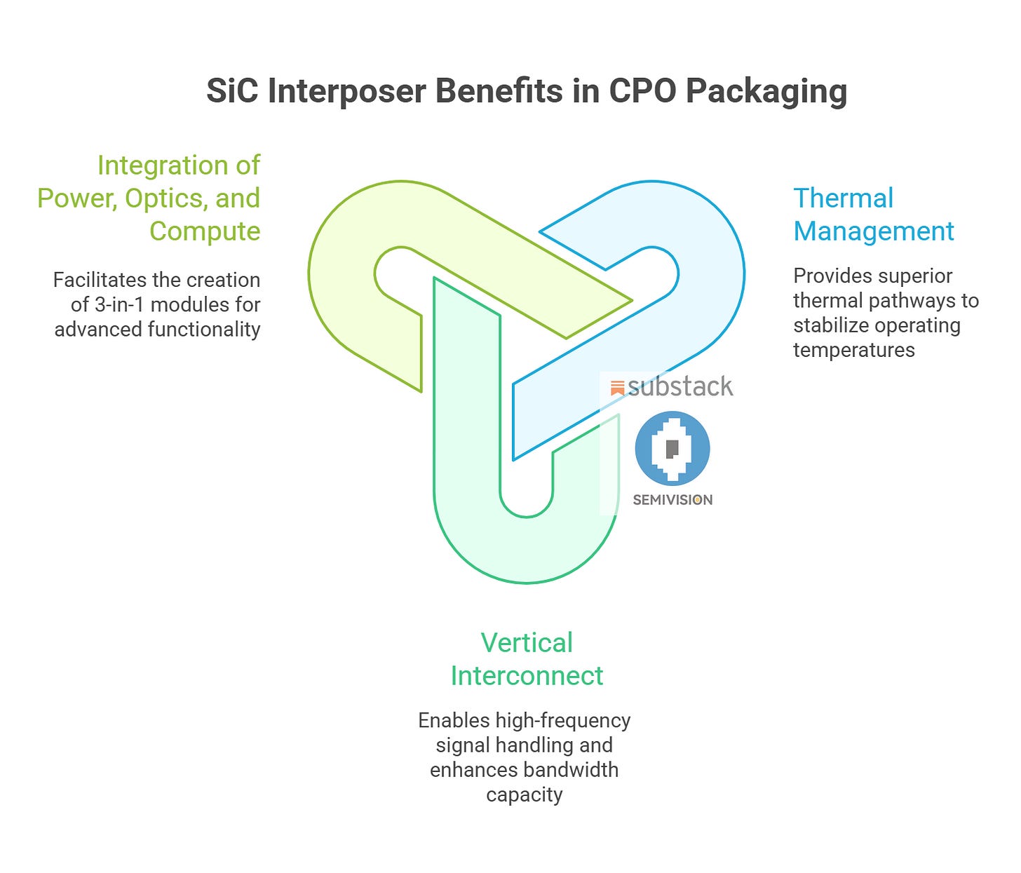
SiC interposers provide superior thermal pathways, stabilizing PIC operating temperatures and preventinglaser wavelength drift or failure.
Vertical interconnect and photonic integration
By employingTSiCVs, SiC interposers can form vertical vias to connect stacked dies or photonic engines, capable of handlinghigh currents and high-frequency signals.
Given their superior RF performance compared to silicon TSVs, TSiCVs help enhanceCPO bandwidth capacity.
Integration of power, optics, and compute
SiC can also be used to manufacturepower devicesorMEMS sensors.
One study demonstrated aSiC MEMS pressure sensor mounted on a SiC interposer, showing TSiCV packaging’s potential for harsh-environment sensing.
In the future, ifvoltage regulators, photonic engines, and AI chipscan all be integrated on a single SiC interposer, this would enable highly functionalelectro-optical-power 3-in-1 modules.
Conclusion
The three papers together present a complete research pathway for Through-SiC Vias (TSiCV)—from theoretical modeling, to process development, to experimental validation. High-resistivity SiC offers low-loss, high-speed RF performance, making it suitable for mmWave and RF applications. Etching requires high-power RIE, with DoE optimization achieving etch rates of 2–3 µm/min. Insulation can be achieved with inorganic oxide layers or BCB polymers, and metallization enables functional interposers. Practical demonstrations also showed the integration of SiC interposers with MEMS modules.
Compared with TSV, TGV, and TCV, TSiCV uniquely combines high thermal conductivity, favorable resistivity, and mechanical robustness, delivering solutions that balance both heat dissipation and signal integrity in high-power, high-frequency domains. However, manufacturing cost and processing complexity remain major challenges.
As AI and datacenters move toward Co-Packaged Optics (CPO), packaging must handle higher power densities and faster electro-optical interconnects. Recent industry reports reveal that NVIDIA and TSMC plan to adopt SiC interposers around 2027 to overcome thermal management bottlenecks. With its superior thermal conductivity and RF performance, SiC is poised to play a critical role in future CPO/AI hardware, especially in high-power systems requiring the co-integration of AI processors, photonic chips, and power modules.
Si CMOS + GaN/SiC

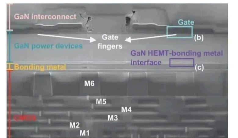
Top schematic illustration:
Left and right sides showSource/Drain, with standard CMOS devices such asP-wellandN-wellin the middle.
Below is thepower device blockintegratingwide-bandgap (WBG) materialssuch asSiCorGaN.
TheBonding SiO₂ interfaceis highlighted, showing how heterogeneous materials are combined throughwafer bonding.
The technology path representsBCD (Bipolar-CMOS-DMOS)integration with WBG devices, targetinghigh-voltage, high-efficiency power applications.
Bottom cross-sectional SEM image:
Clearly shows the stacked structure of aGaN HEMT deviceover the CMOS layer.
M1–M6denote the metal interconnect layers; theGaN transistoris placed on top and integrated withSi CMOSthrough bonding metal.
Labels such asGaN interconnectandHEMT interfacedemonstrate theheterogeneous stacking of power devices and logic control.
Significance:
Demonstratesmonolithic integration of GaN/SiC with Si CMOS.
The core objective is to combinehigh-speed logic (CMOS)withhigh-voltage power devices (GaN/SiC)on the same chip or module, thereby improvingpower conversion efficiency—ideal forAI/HPC power managementandEV applications.
This reflects amajor industry trend, with companies such asIntel, TSMC, STMicro, and Navitasactively developing such solutions.
PDN and Thermal Management – Industry Solutions Overview: Marvell × ASE × TSMC
1) Marvell: Package-Integrated Power and Multi-Chip Packaging Platform
PIVR (Package-Integrated Voltage Regulator) Solution
In mid-2025, Marvell officially launched itsPIVR (Package-Integrated Voltage Regulator)architecture, which places the VRMunder, near, or inside the package—closer to the load.
This approach shortens the power delivery path, lowers PDN impedance, and reducesIR drop and transient droop. Marvell emphasizes that this method improves efficiency and ROI for hyperscale cloud operators in AI/Cloud platforms.
This direction is consistent with the “embedded IVR in CoWoS-L” concept (though here it is presented as Marvell’s general-purpose platform).
In addition, Marvell and Empower Semiconductor announced a collaboration to deliverpre-validated IVR power modulesas drop-in packages that can be co-integrated with custom XPU packaging—accelerating adoption by hyperscale customers.
The key point: IVR requiresfewer capacitors, enablesnear-load regulation, and improves bothbandwidth and efficiency.
Multi-Chip / RDL Platform (Chiplet + HBM + Passive Integration)
Marvell also introduced an advanced packaging platform for custom AI accelerators, supporting integration ofpassive components(e.g., decoupling and filtering capacitors) directly into the package.
This reduces PDN noise inside the package while maintaining expandability for HBM3/3E integration via RDL and multi-chip design.
The goal is toshorten time-to-market (TTM)while providingsupply chain flexibility.
The Shift Toward “Power-at-the-Load” (PoL)
With PIVR,point-of-load regulationis moving from the board level into the package level. By relocating fast, high-frequency VRMs right next to—or directly under—the load, the PDN target impedance requirement is significantly reduced.
IVR-Compatible Low-Capacitance / Small-Package Strategy
High-bandwidth regulation reduces the need for large bulk capacitors. Only a small number of compact capacitors are required inside the package to meet PDN targets.
This strategy complements the CoWoS-L / eDTC approach, where embedded decoupling capacitors further enhance system-level PDN stability.
TSMC: CoWoS-L with Embedded IVR / eDTC + BSPDN + Advanced Cooling (DLC, Microchannel, TIM/Underfill)
2025年5月27日
CoWoS-L with Embedded IVR / eDTC
At its technology forum and IEDM presentations, TSMC highlighted its roadmap forkilowatt-class IVRandeDTC (embedded Deep Trench Capacitor), aimed at boostingvertical power densityandnear-load decoupling. These solutions are explicitly targeting the>1000A–2000A eraof AI GPUs. External reports note that TSMC’s IVR can deliver up to5× the vertical power densityof discrete VR solutions—perfectly aligned with the industry’s move towardembedded IVR / eDTC within CoWoS-L.
BSPDN (Backside Power Delivery Network)
For advanced nodes, TSMC is also pushingSPR (Super Power Rail) backside power, conceptually similar to Intel’s PowerVia: moving thick power rails to the wafer backside while signal routing remains on the front side. This reduces IR drop, eases frontside routing congestion, and also enablesdual-sided cooling—matching the BSPDN direction noted earlier.
Thermal Solutions: DLC, Microchannel, TIM/Underfill
Together with ecosystem partners (system OEMs, cold-plate suppliers), TSMC is evaluatingdirect-to-chip liquid cooling (DLC)andmicrochannel structuresto bring coolant closer to the heat source and lower thermal resistance. Such approaches are often co-designed with BSPDN packaging, as backside metal layers and backside cooling are synergistic.
TIM (thermal interface materials) and underfill selection are also being revisited, with new requirements forhigher thermal conductivity, adhesion strength, CTE matching, and vacuum fill reliabilityas package size grows and cooling architectures evolve.
Integration Perspective: IVR + eDTC + BSPDN
Power delivery, decoupling, and routing unified at the package / wafer backside.
Material × PDN × Thermal: A Three-in-One Approach
SiC × PDN:As a high-voltage, high-thermal-conductivity substrate, SiC can act as the foundation for HVIC and packaging bases. Coupled with IVR / eDTC, it enables near-load power delivery with dense decoupling. For large-scale 2.5D/3D packages (Chiplet + HBM), SiC’s high thermal conductivity and rigidity help suppress warpage and dissipate heat.
SiC × Optical Interconnect:In CPO / SiPh / LN modulator contexts, SiC’s high thermal conductivity and high resistivity balancethermal stabilitywithlow high-frequency loss. This aligns naturally with ASE’s CPO / SiPh platforms and TSMC’s COUPE / SoIC roadmap.
NVIDIA and hyperscalers are already treatingpower and thermalas first-principles design problems, pushing the supply chain (TSMC / ASE / Marvell / Empower, etc.) to co-innovate inpackage-level PDN and liquid/microchannel cooling. This urgency explains whySiC substrateshave become a hot topic and are accelerating toward proof-of-concept (PoC) adoption.
GlobalWafers: 12-Inch SiC Wafer Breakthrough
In mid-September,GlobalWafersannounced a new12-inch SiC wafer technology, highlighting SiC’ssuperior thermal conductivity (~490 W/m·K). This directly addresses the industry’s growing focus onSiC as a thermal substrate.
Earlier, some had proposedplating or coating approachesfor integrating SiC into thermal layers. However, experiments showed poor heat transfer efficiency and high interfacial thermal resistance, leading to disappointing results.
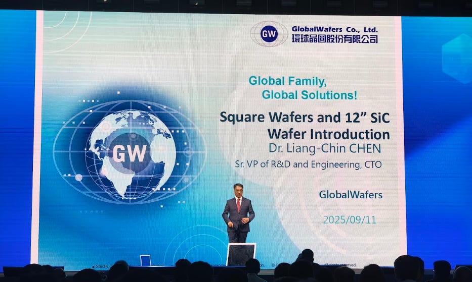
GlobalWafers’ new concept instead resembles acarrier wafer architecture: inserting afull SiC carrier waferdirectly into the package stack as a structural and thermal layer.
This eliminates interface resistance issues from coating schemes.
It maximizes SiC’s intrinsic conductivity, ensuring massive GPU + HBM heat flux can be conducted and spread efficiently.
Division of Functions: Conduction vs. Heat Dissipation
Electrical interconnect remains on thesilicon interposer, preserving mature electrical compatibility.
TheSiC carrier waferfocuses purely on heat conduction—acting as a “thermal acceleration layer.”
This“electrical-thermal separation”strategy reduces yield risk and avoids disrupting the mature silicon interposer supply chain.
Effectively, anew SiC carrier layeris added at the package bottom, relieving vertical thermal bottlenecks. Initial tests show it can significantly reduce heat buildup under high workloads, stabilizing GPU performance—particularly critical for>1000 W-class HPC / AI server chips.

2025年9月16日


PreviousNext
TopLatestDiscussions








See all