SEMICON Taiwan 2025 Material Forum Review
SEMICON Taiwan 2025 Material Forum Review
- Source: SemiVision
- Author: SEMIVISION
- Published: 2025-09-16T14:04:08+08:00
- URL: https://tspasemiconductor.substack.com/p/semicon-taiwan-2025-material-forum SEMICON Taiwan 2025 Material Forum Review - SEMIVISION @_@


SEMICON Taiwan 2025 Material Forum Review
Original Article by SemiVision Research (TSMC , Nvidia , ASE, Tok, GlobalWafers, Lam, AGC, Entegris)

Sep 16, 2025
∙ Paid
In the era of hyperscale computing driven by AI, the semiconductor industry is undergoing an unprecedented transformation. For the past forty years, progress centered on transistor scaling and process shrinks. Today, however, the determinants of system performance and energy efficiency are shifting rapidly toward advanced packaging and materials innovation.
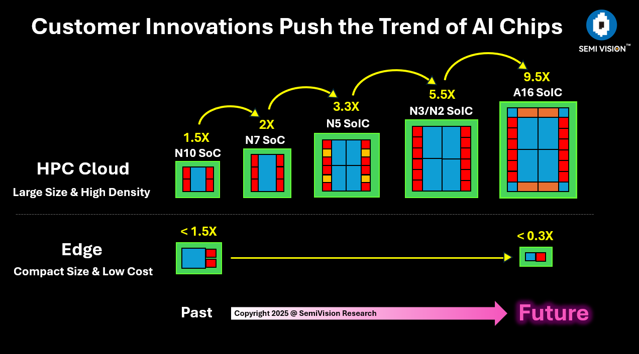
Take TSMC’s CoWoS platform as an example. What began with 2.5D silicon interposers roughly 1.5× reticle in size has expanded to 3.3×, 5.5×, and even 9.5× mega-interconnect fabrics. Packaging itself has become the engine of system-level performance. At these scales, the package not only carries single compute dies measuring hundreds of square millimeters, but also integrates dozens of HBM stacks—elevating “packaging” from a supporting role to a system architecture equivalent to a mega-die.
This trajectory of heterogeneous integration signals a new paradigm: breakthroughs in system performance no longer depend solely on logic node scaling; they require the co-design of advanced package architectures, interconnect/material innovations, and power/thermal solutions. Yet bringing silicon and polymers, metals and glass, photonics and electronics onto one platform introduces challenges around thermal stress, interfacial compatibility, and long-term reliability. This is not just technical evolution—it is a comprehensive race spanning materials science, process engineering, and supply-chain collaboration.
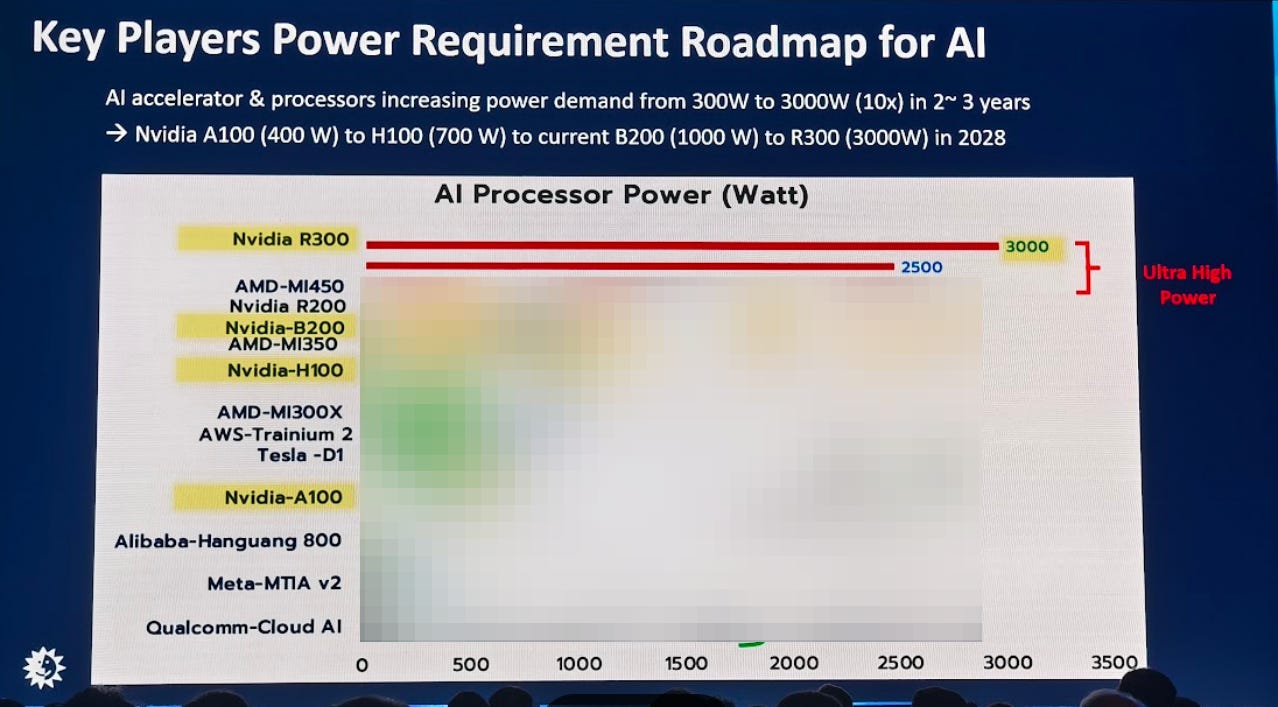
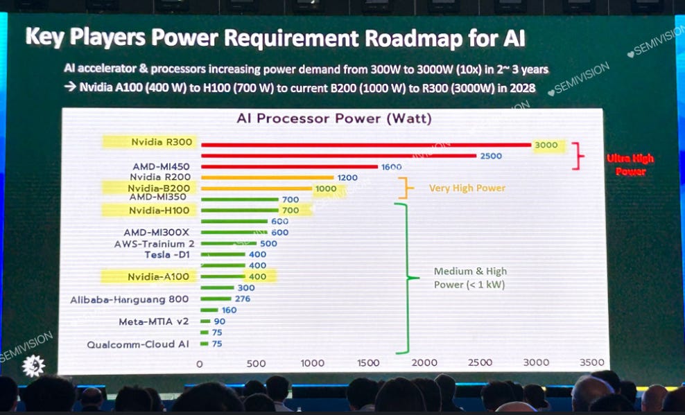
Meanwhile, as GPU power climbs into the kilowatt class—and potentially 3,000 W per device—the power delivery network (PDN), thermal materials, and even substrate form factors (shifting from round wafers toward square silicon panels or SiC interposers) become decisive for sustainable operation. Innovations from chemical-materials suppliers—EUV resists, thick-film packaging photoresists, and low-Dk/low-Df glass substrates—together with equipment vendors, OSATs, and silicon-photonics solutions, are collectively propelling a materials-driven Moore’s Law.
In short, the AI era is no longer a contest of a single company or a single process node. It is cross-disciplinary and cross-supply-chain. Those who lead in materials innovation, packaging architecture, and power & thermal engineering will command the high ground in a trillion-dollar AI market.
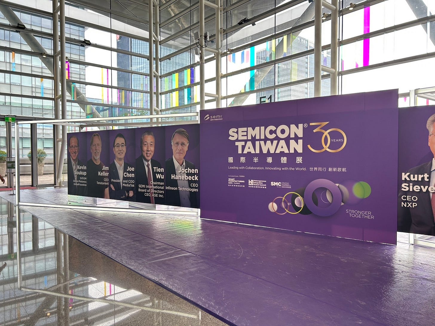
Opening Remarks – SEMICON Taiwan Materials Forum
At this pivotal moment of accelerated transformation in the global semiconductor industry,materialsare moving to center stage. In the past, our focus gravitated toward process scaling, chip architectures, or packaging technologies. Today it is increasingly clear that whether it’s logic (GAA/CFET),1,000-layer 3D NAND, or the 2.5D/3D heterogeneous integration demanded by the AI era, the true determinant of feasibility and success often lies inbreakthroughs in materials.
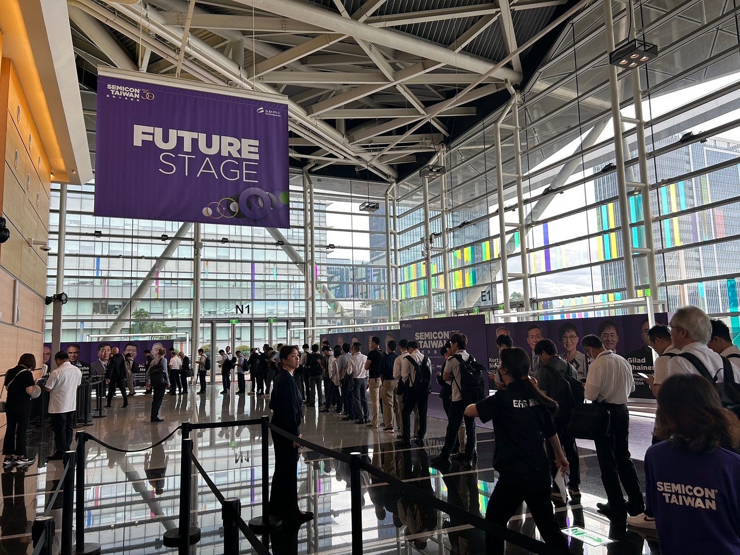
This year’s SEMICON Taiwan Materials Forum is set against that backdrop. We focus onhow materials innovation drives both advanced process nodes and advanced packaging, and we extend the discussion toESG and sustainability. From front-endEUV photoresists and molecular resiststo back-endthick-film photoresists, TGV glass cores, adhesives for advanced packaging, and thermal interface materials, the evolution of materials determines not only performance, but alsoyield, reliability, and supply-chain competitiveness.
Throughout the forum, we heard perspectives from leading materials companies, equipment suppliers, and OSATs. A shared message emerged: the future extension ofMoore’s Lawwill rely increasingly onmaterials science. For example,TOKshowcased the potential of metal-containing resists and molecular resists under EUV;GlobalWafersproposedsquare silicon panelsandSiC interposersas new options for high-power packaging; andAGChighlightedTGV glass coresandlow-Dk/low-Df glassfor AI datacenters and photonic integration.
Equally important, materials innovation has shifted from isolated breakthroughs tocross-industry, cross-disciplinary collaboration. The forum repeatedly emphasized that only through open cooperation—among chemical suppliers, equipment vendors, foundries, and system companies—can we shorten development cycles while ensuring manufacturability and high-volume reliability.
Therefore, the Materials Forum is more than a technical exchange; it is aplatform for ecosystem dialogue. It reminds us that in the age of AI and advanced packaging, the core driver is not merely the number of transistors, butsystem-level solutions shaped jointly by materials and architecture.
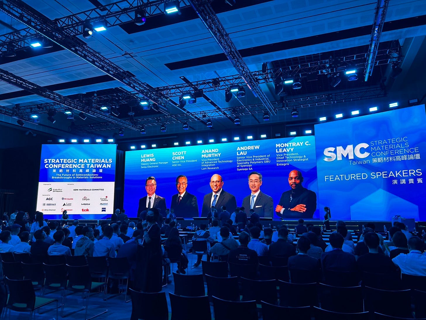
In today’s rapidly expanding landscape of AI, HPC, and advanced packaging,materials scienceis becoming the core source of competitive advantage for the semiconductor industry. In this context, theStrategic Materials Conference Taiwan (SMC Taiwan) at SEMICON Taiwan 2025brings together top speakers from global industry and R&D. From front-end lithography and thin films to back-end packaging, thermal interfaces, and sustainable material design, the forum presents a panoramic view of materials innovation.
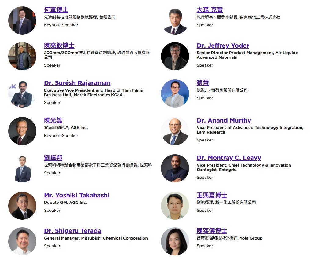
TheKeynoteaddresses will be delivered byDr. Jun He(Vice President, Advanced Packaging Technology & Service,TSMC) andMr. Scott Chen(Senior Vice President,ASE), outlining tool and material needs and the challenges for3DIC/advanced packagingin the AI era.
The speaker lineup spans both materials suppliers and hands-on experts from packaging and manufacturing:
Katsumi Omori(TOK) will discuss materials solutions for front-end and back-end lithography.
Dr. Liang-Chin Chenwill offer foundry/wafer-supplier perspectives on the potential ofsquare silicon panelsfor advanced packaging.
Dr. Suresh Rajaraman(Merck) andDr. Montray C. Leavy(Entegris) will present advances in thin-film materials, novel chemistries, and surface/interface engineering.
ZEISSandDr. Yik Yee Tan(Yole Group) will address materials analytics, package reliability, supply-chain and market trends—emphasizing the roles of materials validation and sustainable design.
This diverse roster is more than a technical showcase; it reflects a broader trend: the next phase of semiconductor competition is not only about process scaling, but an integrated race—frommaterial composition, interfaces, and manufacturabilitytopackage architectureandsystem efficiency. Topics include howALD chemistry/ligand tuningimpacts process performance; the thermal and mechanical challenges ofsquare panelsandglass/dielectric substratesin packaging; the introduction offluorine-free surfactantsand sustainable materials into manufacturing supply chains; and how material/tool suppliers can collaborate with OSATs and foundries to reduce yield risk and shorten time-to-market.
In short,SMC Taiwan 2025is not only a venue for technical exchange—it is a milestone advancing materials innovation and supply-chain collaboration to the next level. For anyone focused onAI, 3DIC, advanced packaging, or even quantum/HPC, this forum will deliver front-line insights and a clear direction for aligning technologies, materials, and markets.
For Paid Members, SemiVision will discuss topics
TSMC : Addressing the Unprecedented Challenges in Advanced Semiconductor Manufacturing
TOK: Material Development Strategy and Progress in Advanced Semiconductor Manufacturing
GlobalWafers: Square Silicon Wafers and SiC Interposers: Strategic Push for Next-Generation Substrates
ASE: Advanced Packaging and Materials at the Center of the AI Era
Lam: The Future of Semiconductors: Breakthrough in Materials Solutions
Entegris: Materials Innovation and Advanced Packaging: At the Core of the AI Era
AGC: Integrating Glass Solution in Advanced Packaging
If readers would like to learn more about the key takeaways from the Semicon Taiwan technical forums, SemiVision has compiled a related report. Please feel free to reach out to us at: jett@semivisiontw.com & eddyt@semivisiontw.com
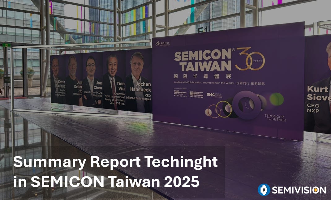

TSMC : Addressing the Unprecedented Challenges in Advanced Semiconductor Manufacturing
The semiconductor industry is entering a transformative era, defined by rapid technological progress, intensifying economic pressures, and growing operational complexity. Nowhere is this more evident than inadvanced packaging and heterogeneous integration, where the scale and intricacy of modern integrated circuits are forcing the industry to rethink long-standing practices. As Dr. He emphasized in a recent keynote, tackling these challenges requires unprecedented levels ofcollaboration across the entire supply chain.

Advanced packaging is emerging as one of the key enablers for AI computing, and the industry is now scaling 2.5D/3D integration to unprecedented levels. TSMC’s CoWoS (Chip-on-Wafer-on-Substrate) platform illustrates this trajectory clearly. Over the past decade, CoWoS-S has matured into high-volume production, reaching interposer sizes up to 3.3 reticles. Building on that foundation, CoWoS-L and CoWoS-R are extending scaling further, pushing towards 5.5-reticle and even 9.5-reticle interposers, capable of hosting massive SoCs alongside dozens of HBM stacks.
This trend reflects two central imperatives in AI-era semiconductor design:more bandwidth and more integration. Larger interposers allow not just bigger compute dies but also tighter coupling with high-bandwidth memory (HBM3E/4), reducing data transfer bottlenecks. At the same time, heterogeneous integration—placing multiple SoCs, accelerators, and memory in a single advanced package—turns a collection of dies into what functions like one giant chip.
A roadmap where packaging becomes asystem-level performance driver, no longer a supporting afterthought. Scaling from 1.5 to 9.5 reticles means packaging is now central to enabling next-generation AI workloads. The trajectory suggests that future breakthroughs in compute efficiency will depend as much onpackaging architecture and materials innovationas on logic scaling itself.
The Imperative of Heterogeneous Integration
Heterogeneous integration has emerged as one of the most disruptive shifts in semiconductor design—an approach that “everybody loves” because of the new possibilities it enables. Yet, from a physics and materials science perspective, it introduces formidable hurdles. Placing polymers next to silicon, for instance, brings together materials with radically different mechanical and thermal expansion properties, creating fragile interfaces vulnerable to reliability issues.
These challenges—interface stability, chemical compatibility, and process complexity—cannot be solved through single, linear development cycles. Instead, they demandrapid, iterative co-developmentamong suppliers and device makers, backed bydedicated engineering teamscapable of fast prototyping and foundational setup.
Economic and Infrastructure Transformations
The scale of integration continues to escalate. Industry discussions now include moving from8-high to 6-high stack layers, a shift that amplifies the economic value of each integrated component. In this environment, even a1% yield improvementcan translate into enormous financial gains.
At the same time, the industry is confronting theeconomic inefficiency of circular wafers. As packages grow larger and square in shape, round wafers waste significant “real estate.” This basic principle of economics is driving the exploration ofnew wafer shapesto maximize usable area. Such a move would not be incremental—it would demand acomplete overhaul of infrastructure, including new material delivery systems, handling frames, cassettes, and trays, with ripple effects across the supply chain.
Automation, Metrology, and Supply Chain Coordination
Automation and precision detection are critical to handling the complexity of advanced chip assembly. With multiple dies in a single package, defects must be identifiedimmediatelyto avoid costly downstream failures. Yet today, there remains “too much manual work” across the supply chain, constraining efficiency and hindering global scalability amid geopolitical pressures.
Collaboration between toolmakers and material suppliers is vital to automate steps such asbonding-head changes and tooling adjustments. Meanwhile,metrologyis becoming a central pillar of yield control. Detecting process excursions “upfront” requires scaling up measurement capabilities, with packages potentially demanding20 separate alignment checksat micron-level precision. What took the front-end ecosystem 30 years to build must now be accelerated dramatically to meet the unprecedented demands of 3D integration.
ESG and the Call for Collaboration
Environmental, Social, and Governance (ESG) imperatives can no longer be treated as afterthoughts. Instead, they must be embedded “from the very beginning” of technology development cycles, driven by regulatory demands and a global push toward sustainability. A greener planet is not just a goal—it is becoming adesign constraint.
Above all, the industry needstransparency and open collaboration, particularly in material R&D. Given the high-risk nature of advanced semiconductor manufacturing, no single company can tackle these challenges in isolation. Shared knowledge and joint innovation are the only viable paths forward.

2025年5月17日
Optimism Amid Challenges
Dr. He closed on a note of optimism, pointing to past breakthroughs at7nm, 5nm, and 3nmnodes as proof that the industry can overcome seemingly insurmountable hurdles through collective effort.
Together, these discussions underscore a common message: the semiconductor industry is not shying away from its toughest problems. Instead, it is leaning into them—throughinnovation, cross-disciplinary partnerships, and systemic rethinking—to pave the way for the next era of advanced semiconductor manufacturing.
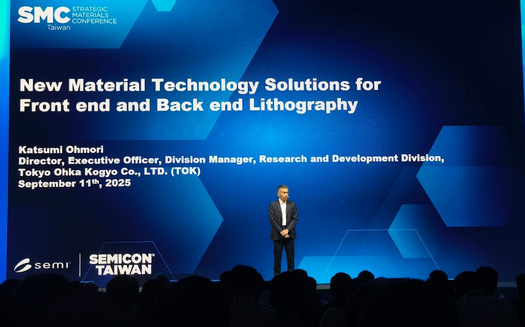
TOK: Material Development Strategy and Progress in Advanced Semiconductor Manufacturing
At a recent industry conference, Tokyo Ohka Kogyo (TOK) presented itsmaterial development strategy and progressin both front-end lithography and advanced packaging. The session highlighted not only the technical challenges faced by next-generation semiconductor manufacturing, but also the company’s efforts in sustainability and supply-chain collaboration.
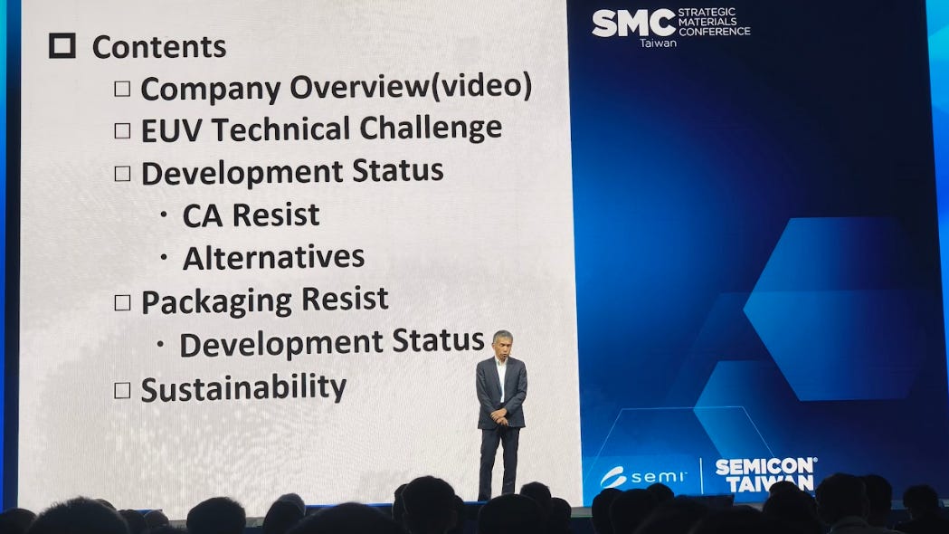
TOK framed its vision around a theme ofprogress through chemistry. While semiconductors are indispensable to the digital economy, photoresists remain indispensable to semiconductor manufacturing itself. As one of the leading global suppliers of photoresists, TOK emphasized its commitment to continuous innovation, quality improvement, and contribution to society. The company’s message positioned itself as a key enabler of technological progress, with sustainable growth underpinned by advanced chemical development.
Front-End Material Development
The presentation underscored the escalating demands ofEUV lithographyfor advanced logic devices. A central challenge remains thetrade-off between sensitivity and resolution, compounded by requirements for improved etch resistance and defectivity control.
TOK’s long history in chemical supply provides an advantage inquality control and impurity management, essential for minimizing defects. Two main development pathways were outlined:
Metal-containing resists: offering high EUV absorption, stability, and compatibility with existing spin-coating processes.
Molecular resists: providing strong absorption, reduced line-edge roughness, and enhanced resolution at smaller nodes.
Demonstrations included sub-12 nm patterning with thin films around 70 nm, suggesting readiness for next-generation lithography nodes.
Materials for Advanced Packaging
Attention also turned to the packaging domain, where material requirements differ sharply from front-end processes. Advanced 2.5D/3D packages demandthick resists(10–100 μm), robust plating performance, and etch resistance under both conventional and cryogenic conditions.
Key developments included:
Fine-pitch resist performance enabling2 μm line/space featuresin 7 μm films.
Microvia resists with stable 22 μm thickness and clean development profiles.
Etching materials capable of withstanding-40°C to +100°Cenvironments.
Thick-film solutions up to 390 μm, maintaining vertical profiles and suppressing cracking issues.
Sustainability as a Development Driver
Sustainability was identified as a critical pillar of TOK’s material R&D. The company is advancingPFAS-free resistswith comparable performance to conventional chemically amplified systems and has developedtopcoat-free immersion resiststo eliminate fluorine additives while preserving lithographic performance. These initiatives reflect growing regulatory and customer demands for environmentally responsible solutions.
The presentation positioned TOK as both atechnology leader and ecosystem collaborator. The company highlighted partnerships with equipment and material suppliers such as TEL, Lam Research, and Applied Materials, stressing the importance of cross-industry engagement in overcoming scaling bottlenecks.
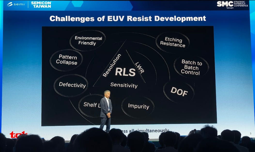
EUV resist development sits at the heart of next-generation semiconductor scaling. While extreme ultraviolet lithography (EUVL) enables critical dimensions at the 5nm, 3nm, and future 2nm nodes, the resist materials face multiple, often conflicting requirements. The well-knownRLS trade-off(Resolution–Line Edge Roughness–Sensitivity) illustrates the difficulty: improving one parameter often worsens another. Beyond this, numerous secondary factors—etch resistance, defectivity, pattern collapse, and environmental compatibility—further complicate material design.
These simultaneous challenges, which material suppliers and semiconductor manufacturers must address in tandem. Success in EUV resist development requires balancing not only the RLS triangle but also production consistency, sustainability, and manufacturability.

The broader takeaway is clear:chemistry remains a critical lever for semiconductor advancement. Whether in EUV resist performance, packaging materials for 3D integration, or sustainable alternatives to legacy chemicals, material innovation is becoming a decisive factor in enabling next-generation nodes and system architectures.

GlobalWafers: Square Silicon Wafers and SiC Interposers: Strategic Push for Next-Generation Substrates
At the recent industry conference, GlobalWafers outlined a bold vision for reshaping semiconductor packaging substrates through innovations insquare silicon wafersandSiC interposer technology. The company’s message was clear: as the industry pushes deeper into heterogeneous integration, chiplet architectures, and high-power applications, new substrate materials and formats will become critical enablers.

Rethinking the Substrate: From Round to Square
Traditionally, semiconductor wafers have been round—a legacy of crystal growth and wafer slicing methods. However, this circular geometry creates inefficiencies when moving into advanced packaging, particularly when substrates are needed in panel form. GWC presented the concept ofsquare silicon wafers (310×310 mm and 510×515 mm)as a way to overcome these inefficiencies.

Compared to glass, which has attracted attention for panel-level packaging, silicon offers distinct advantages:
Flatness: Both silicon and glass can achieve <10 µm, suitable for fine-pitch interconnects.
Elastic Modulus: Silicon’s 165 GPa far exceeds glass (50–90 GPa), ensuring greater mechanical robustness.
Thermal Conductivity: Silicon offers ~148 W/m·K versus just ~1 W/m·K for glass, addressing one of the most pressing bottlenecks in high-power AI and HPC devices—heat dissipation.
In other words, while glass remains attractive for certain cost-sensitive or RF applications,square silicon substrates could balance manufacturability, thermal performance, and scalability, offering a direct alternative for next-generation interposers.
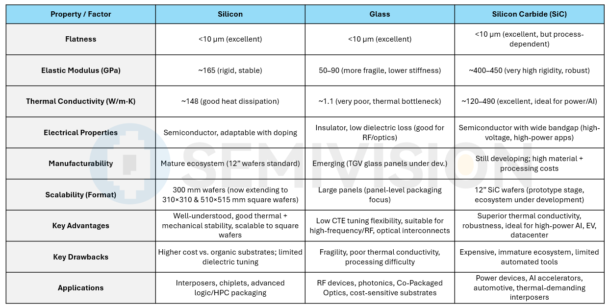
Glassis attractive for RF/optical but struggles with heat.
Siliconremains the balanced “workhorse,” especially with square wafer innovations.
SiCis strategically important forthermal + power-heavy AI and EV applicationsdespite higher costs.
Crystal Growth Pathways: Scaling Up Production
GlobalWafers emphasized that square wafers are not merely a geometric change but require rethinking crystal growth. For310×310 mm, both single crystal and polycrystalline approaches are possible, while the larger510×515 mmformat may rely on polycrystal or “mono-like” growth.
The company highlighted process innovations inmono-silicon growth—from seeding and necking through full-body formation—as well as adaptations forpoly-Si and block preparation. These methods aim to minimize silicon loss while enabling new ingot geometries tailored for square slicing.
The key takeaway is thatproduction technology for large-area substrates is maturing, and square wafers could realistically enter high-volume manufacturing once ecosystem alignment occurs.
SiC Interposer Technology: Enabling Power and Thermal Management
Equally significant is GWC’s push intosilicon carbide (SiC) interposer technology. As AI accelerators and power devices scale to kilowatt-class consumption, thermal conductivity becomes paramount. SiC, with its superior heat resistance and mechanical stability, is emerging as a promising alternative to traditional silicon or organic interposers.
GWC showcasedembedded heat pipe SiC interposersfor distributed power devices. These designs integrate vapor bubbles within the SiC matrix, drastically improving thermal conductivity and enabling efficient heat spreading. Cross-sectional micrographs demonstrated fine-pitch vias (40–100 µm) metallized with copper, compatible with flip-chip assembly.
The company cited collaborations with research institutes such as Fraunhofer IZM, underlining that SiC interposers are moving beyond lab experiments towardpractical packaging solutions for power-hungry AI accelerators and automotive applications.
Building an Ecosystem: Square Wafers and 12-Inch SiC
Despite technical progress, GWC acknowledged thatecosystem readiness remains a bottleneck. Automated process equipment for bothsquare silicon wafersand12-inch SiC wafersis still under development. This requires joint efforts withequipment vendors, material suppliers, and end-customersto define tooling, process controls, and metrology standards.
The company called for aglobal SEMI standardto ensure interoperability and accelerate adoption. Much like how 300 mm silicon wafers standardized the modern fab era, the establishment ofecosystem standards for square and SiC waferscould unlock their full economic and technical potential.
Strategic Implications
From an analyst perspective, GWC’s roadmap represents more than incremental improvements—it highlightstwo structural shifts in substrates:
Square Wafer Adoption: Directly addresses real estate efficiency and die placement density in advanced packaging, potentially replacing 12-inch silicon interposers and competing with glass core substrates.
SiC Interposers: Provide a pathway to solve the escalatingthermal bottleneckin AI datacenters, EV power modules, and high-performance computing—areas where traditional silicon or organic substrates struggle.
Both initiatives underscore a broader industry trend:substrates are no longer passive carriers but active performance enablers. Whether in managing warpage, heat, or interconnect density, the substrate is moving closer to the center of semiconductor innovation.
GlobalWafers’ preparation for high-volume manufacturing of310×310 mm square silicon wafersand12-inch SiC waferssignals strong confidence in market adoption within the next five years. Success will hinge on ecosystem alignment, cost competitiveness, and demonstrable advantages in yield and reliability.
If these hurdles are cleared, square wafers and SiC interposers could becomecornerstones of the AI and power electronics era, reshaping supply chains and creating new competitive dynamics across the semiconductor packaging industry.
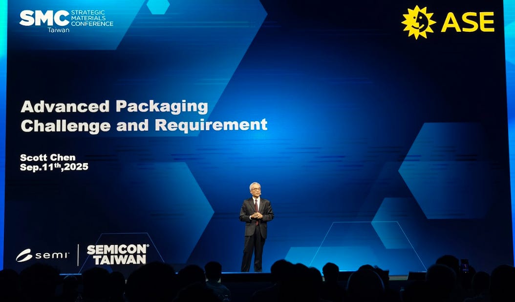
ASE: Advanced Packaging and Materials at the Center of the AI Era
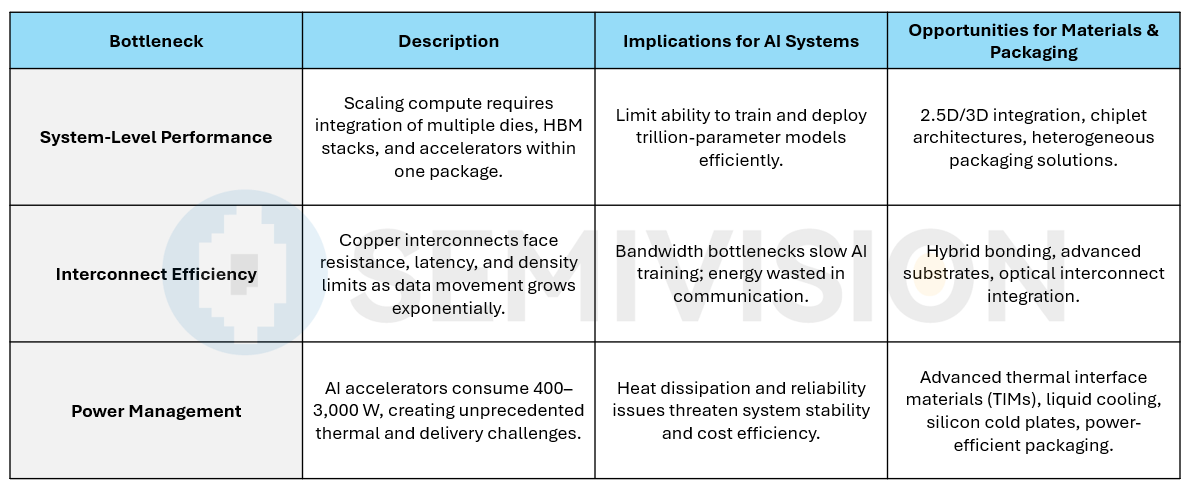
ASE highlighted howadvanced packaging and materials innovationare becoming central pillars in enabling the AI revolution. As the industry transitions from an era defined by transistor scaling to one driven by system-level integration, it is increasingly evident that Moore’s Law alone cannot sustain the exponential growth in compute demand. The company emphasized that whiletransistors and logic scalingremain important, the fundamental bottlenecks in AI hardware no longer reside solely within the silicon itself. Instead, they are shifting toward three interdependent domains:system-level performance, interconnect efficiency, and power management.

First,system-level performanceis increasingly constrained by the need to integrate multiple high-performance dies—such as GPUs, CPUs, AI accelerators, and stacks of high-bandwidth memory—into a single package. This heterogeneous integration introduces challenges in yield, reliability, and scalability, yet it is indispensable for meeting the throughput demands of trillion-parameter AI models.
Second,interconnect efficiencyhas emerged as a critical limiter. Traditional copper interconnects face inherent resistance, signal loss, and density limits, making it difficult to sustain the bandwidth required for AI training and inference workloads. Data movement, rather than raw computation, is now the primary consumer of energy within large-scale systems. To overcome this, ASE and other industry leaders are investing in solutions such as fine-pitch hybrid bonding, advanced substrate technology, and the integration of optical interconnects at the package or even wafer level. These technologies aim to dramatically increase bandwidth while lowering latency and reducing energy-per-bit transmission costs.
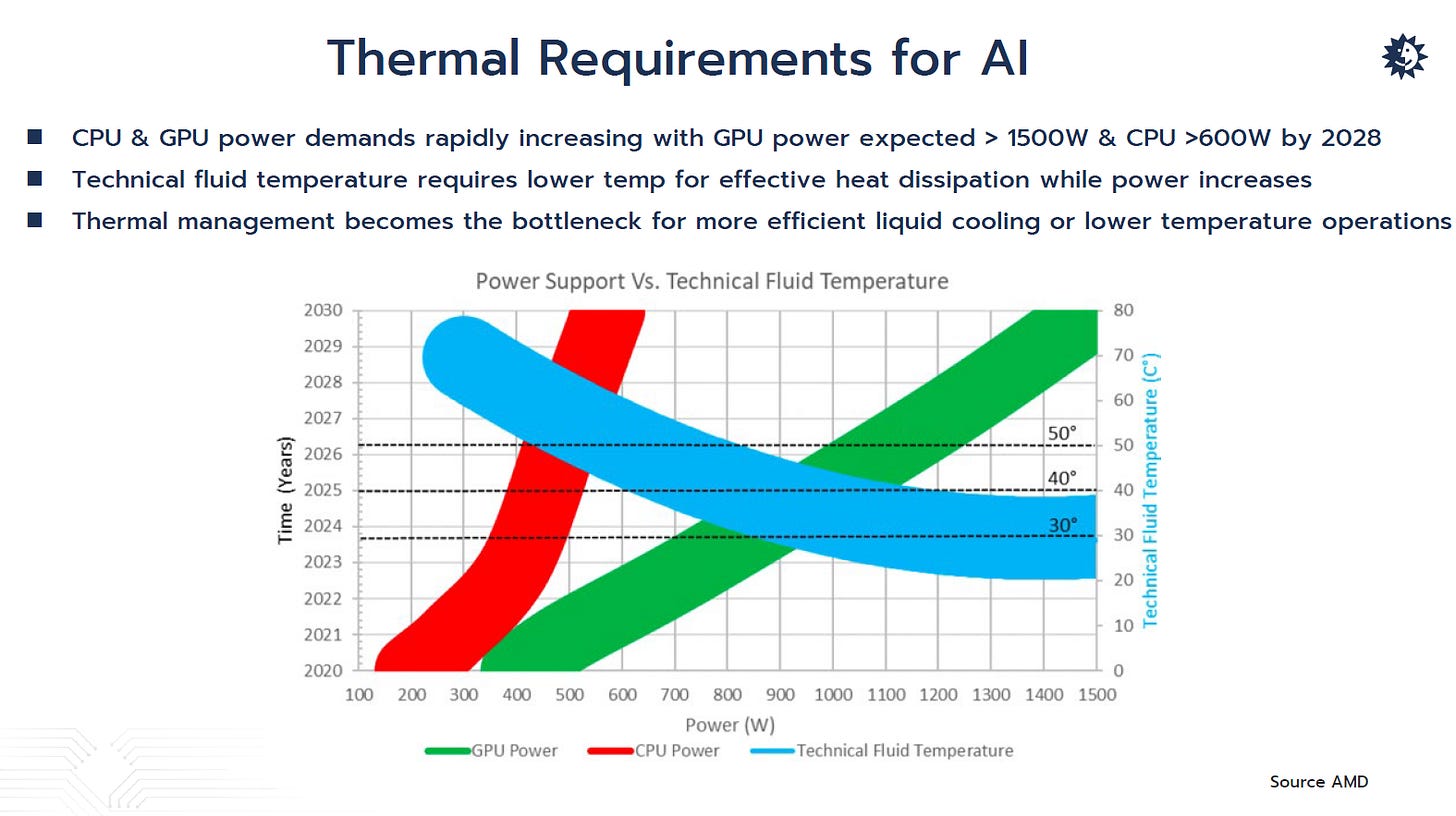
Finally,power managementrepresents perhaps the most urgent and visible challenge. AI accelerators are rapidly scaling from 400 W to beyond 1,000 W per device, with projections of 3,000 W in upcoming generations. This power density creates unprecedented thermal management problems, demanding not only advanced cooling solutions—such as liquid immersion and silicon cold plates—but also breakthroughs in thermal interface materials, stress-resistant substrates, and package-level power delivery networks. Without innovations at the packaging and materials level, these devices cannot operate reliably or economically.
Together, these three bottlenecks—performance, interconnect, and power—are redefining the competitive landscape. In this new environment, success will depend less on transistor density alone and more on the ability of packaging houses, material suppliers, and system integrators toco-innovate across the entire ecosystem. ASE’s emphasis reflects a broader industry consensus: advanced packaging is no longer a supporting technology, but astrategic enabler of the AI era.
Entering the AI Era
The conference underscored that the world is undoubtedly entering theAI era. Forecasts project the AI market to approachUSD 1 trillion by 2030, with high-performance computing expected to capture roughly 40–45% of that value. Mobile devices, automotive platforms, and IoT applications will also absorb AI capabilities, creating broad-based demand across industries.
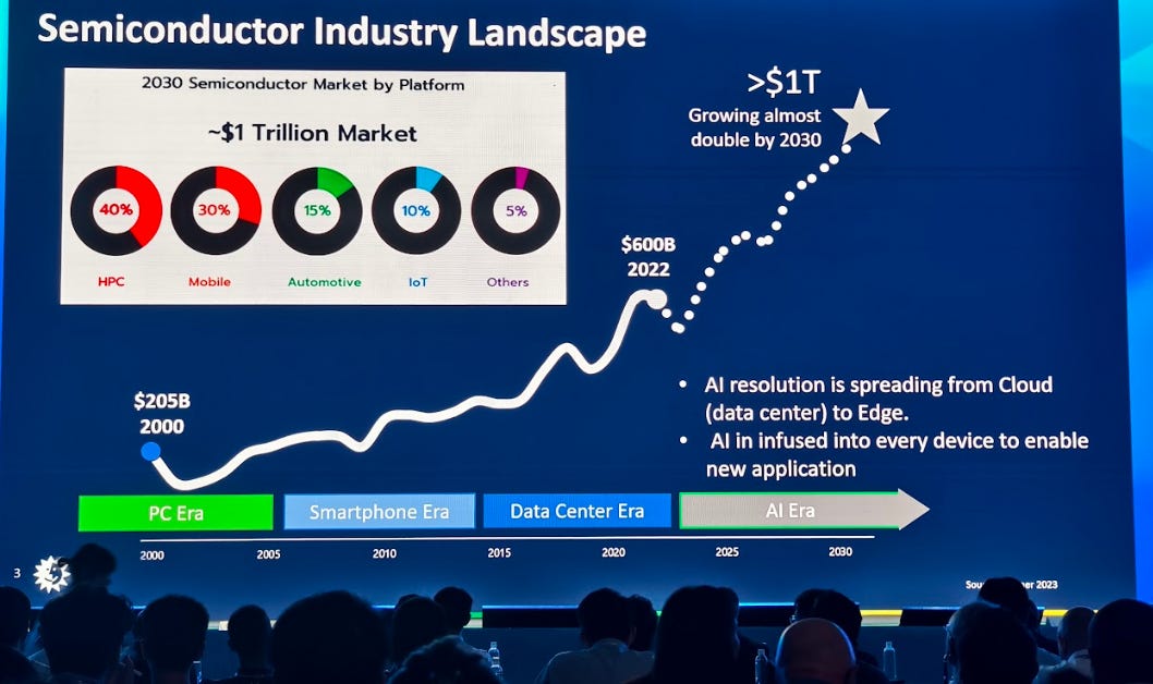
This demand translates directly into semiconductor requirements: compute performance is projected to improve by 2–7× in the near term, memory bandwidth by up to 10×, and interconnect density by an order of magnitude. Yet these gains come at the cost ofpower consumption, with GPUs already moving from 400 W to over 1,000 W per unit, and projections for next-generation AI accelerators reaching 3,000 W.

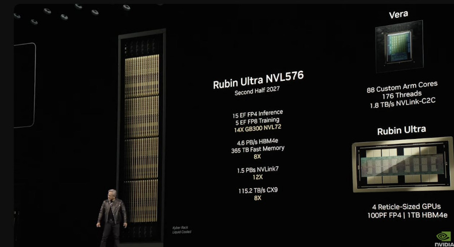
NVIDIA has announced an even more powerful platform —Rubin Ultra, expected in thesecond half of 2027. While theVera CPUwill remain unchanged, the GPU configuration will undergo a major leap forward, integrating up to576 Rubin Ultra GPUswithin the NVL576 system.
15 ExaFLOPS of FP4 inferenceperformance,
5 ExaFLOPS of FP8 trainingcapability,
Roughly4× the compute capacity of the Rubin NVL144system.
This system will be backed by4.6 PB/s of HBM4e bandwidth,365 TB of fast memory, and1.5 PB/s NVLink7 interconnect throughput, with CX9 networking delivering115.2 TB/s— representing unprecedented scale in GPU-based computing.
However, such massive integration bringscritical challenges in power consumption and thermal management. With GPUs already scaling into the multi-kilowatt range, cooling a 576-GPU liquid-cooled supercluster like Rubin Ultra will require substantial innovations in rack-level design, liquid cooling infrastructure, and power delivery systems. The industry must carefully evaluate not only the computational gains but also thesustainability and operational efficiencyof such a power-hungry platform.

Packaging as the Enabler
Advanced packaging has become the critical lever for balancing performance, power, and size.2.5D silicon interposers combined with 3D-stacked HBM memoryare already showing 30–70% reductions in footprint and up to 10× gains in bandwidth efficiency. Fan-out, hybrid bonding, and TSV integration are being deployed not just as assembly solutions, but asstrategic enablers of system-level AI performance.
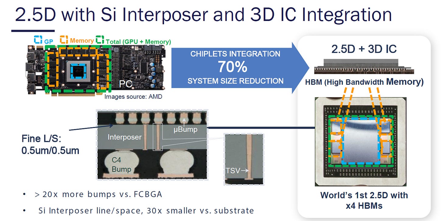
The shift from solder-based joints to copper hybrid bonding exemplifies the industry’s push to minimize interconnect length, reduce resistance, and improve reliability. Still, challenges persist: warpage, joint quality, and thermal stress require not just structural innovation but alsonew classes of materialstailored for thick resists, high-aspect-ratio vias, and robust reliability.
The Thermal Wall
Thermal management remains a defining constraint. With AI accelerators consuming kilowatts of power, traditional liquid cooling is insufficient. New approaches—ranging from silicon cold plates to advanced thermal interface materials and system-level liquid immersion—are emerging, but none yet provide a definitive solution for 3,000 W-class devices. This is a pressing opportunity for material suppliers, who can deliver innovation inheat dissipation, stress control, and high-power reliability.
Photonics and the Interconnect Future
Another recurring theme was the migration from copper to optics. While optical interconnect is already adopted at the system level,integrating photonics directly into advanced packagingis viewed as the next leap. Optical engines embedded at the wafer or panel level promise order-of-magnitude improvements in bandwidth and power efficiency. Yet integration remains complex, involving EIC/PIC co-packaging, lens alignment, and wafer-level processing innovations. This space is still in its early phase, offeringsignificant opportunities for collaboration between semiconductor, optics, and materials ecosystems.

2025年6月18日

Power SiP: Redefining Power Delivery for the AI Era
As AI workloads continue to scale, the semiconductor industry is encountering a growing challenge: how to deliver massive amounts of power efficiently, reliably, and within increasingly constrained form factors. At SEMICON Taiwan, ASE introduced itsPower SiP™(System-in-Package) solution—a transformative approach to power delivery that directly addresses current density limits, I²R losses, and thermal bottlenecks that plague advanced systems today.
The Problem: Rising Power Demands, Shrinking Margins
Modern GPUs and AI accelerators now exceed1,000–3,000 watts per system, with transistor counts and memory stacks driving density beyond anything seen in prior generations. Traditional lateral power delivery structures are reaching their limits. In lateral configurations, current density hovers around0.4 A/mm², with resistive (I²R) losses consuming as much as12% of total power. This not only wastes energy but exacerbates thermal management problems.
The Principle: 3D Vertical Power Integration

ASE’s Power SiP turns the conventional power delivery scheme on its side—literally—by moving from lateral tovertical 3D stacking of power components.
Vertical 3D SiP Gen1increases power density to0.6 A/mm²while reducing resistive loss to6.3%.
Vertical 3D SiP Gen2pushes density to0.9 A/mm²with only3.6% I²R loss, marking a three-fold improvement in efficiency compared to lateral layouts.
This improvement stems from shorter electrical and thermal paths: with capacitors, inductors, and controllers stacked directly above or below the chip, parasitic resistance and inductance are minimized. Heat dissipation becomes more direct, lowering overall power consumption.
Platform Design: VPD and Embedded Technologies
ASE’s Power SiP is not just a single device but aplatform architecture. TheirVPD (Vertical Power Delivery) Technologyconverts high input voltages—typically48V down to <1V—through a staged system of embedded capacitors, inductors, and controllers within the SiP.
Two key innovations stand out:
IVR Embedded (Integrated Voltage Regulator):Achieves total thickness of ~1mm, directly embedding regulators within the package.
SESUB Embedded (IC + Capacitors):Reduces thickness further to ~0.5mm while maintaining stability, critical for compact system boards.
This allows high-performance processors to receive clean, low-voltage power without the need for bulky external regulators, dramatically reducing board-level footprint and transmission losses.
Strategic Importance for AI Systems
The importance of this breakthrough cannot be overstated. In AI factories where thousands of GPUs are deployed, even a2–3% reduction in power losstranslates intomegawatts of saved energy—cutting operational costs and easing data-center sustainability pressures.
Moreover, by reducing lateral footprint and stacking components vertically, ASE enables:
25% reduction in XY area, allowing more silicon per unit board space.
Higher component density, supporting dense HBM and logic co-packaging.
Shorter electrical and thermal paths, improving both speed and reliability.
In other words, Power SiP is more than a packaging innovation; it is aninfrastructure enablerfor the AI era.
ASE’s introduction of Power SiP underscores howpower delivery has become as strategic as logic scaling. While much of the industry focuses on GPUs, interconnect, and memory, the silent enabler is efficient power conversion. As GPUs like NVIDIA’s Rubin and Feynman generations move towards multi-kilowatt operation, vertical power delivery will likely become a standard design feature across high-end AI and data-center systems.
ASE’s strategy also highlights an important industry truth:the bottlenecks of tomorrow are no longer just about transistors but about system-level energy efficiency.Power SiP exemplifies how packaging innovation can directly unlock system performance, reduce costs, and support global sustainability targets.
The ASE discussions at SMC reinforced several critical takeaways:
Packaging is no longer a supporting act; it is the main stage for AI compute.
Materials innovation is inseparable from packaging progress, spanning lithography resists, bonding materials, thermal solutions, and photonics.
The industry faces a dual mandate: improve performance and power efficiency while ensuring manufacturability, reliability, and environmental compliance.
Collaboration across the ecosystem—from foundries to OSATs, from chemical suppliers to toolmakers—will determine how quickly solutions can scale.
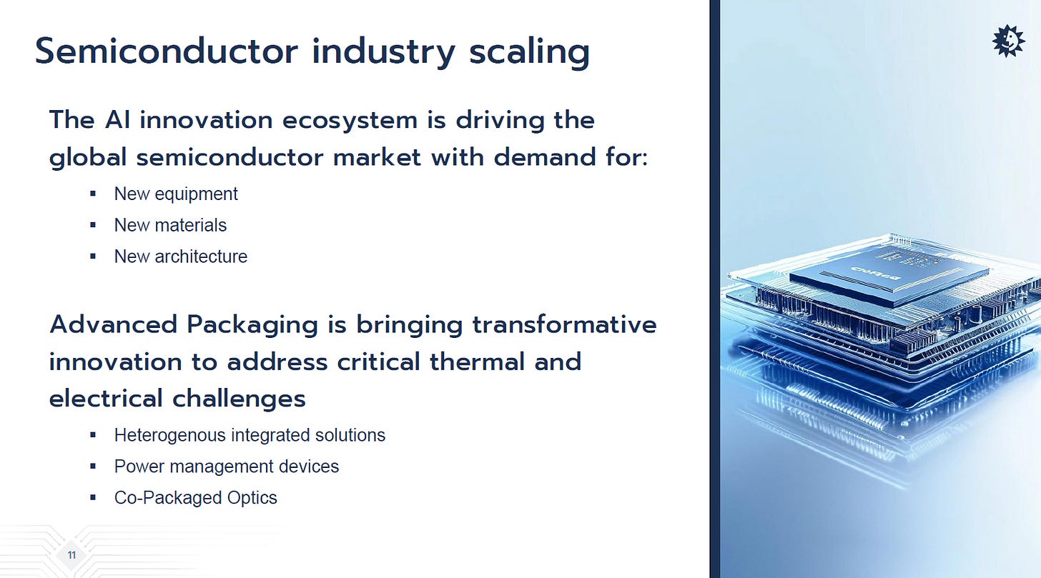
The AI revolution isforcing a redefinition of semiconductor roadmaps, where materials and packaging move from secondary considerations toprimary differentiators. The next decade will not be defined solely by transistor density, but by how well the industry masterssystem integration, thermal management, and optical interconnects.

Lam: The Future of Semiconductors: Breakthrough in Materials Solutions
AI is forcing the entire semiconductor stack to change faster than any period in recent memory. Hyperscalers are committing an unprecedented$20–25B per quarterof capex, pulling logic, memory and storage onto steeper roadmaps. Yet the limiting factors are no longer just transistor dimensions; they areinterconnect resistance, vertical integration complexity, and power/thermal budgets. Across logic, DRAM, and 3D NAND, the common denominator is materials: deposition chemistries, liners/barriers, selective films, and low-loss dielectrics that make dense 3D architectures manufacturable.
A central thesis emerging from the sessions is thatmolybdenum (Mo)—grown with atomic/area-selective processes and engineered for large grains—has become the leading candidate to succeed or flank Cu/Co/W at advanced dimensions. NAND provides the clearest case study: after a decade in which ALD/CVDtungsten (W)enabled high-aspect-ratio fills, the industry’s next resistance and stress reductions will come frombarrier-light or barrier-free Mo wordlinesand Mo contacts/interconnects in logic and DRAM. The following analysis synthesizes the technical arguments, integration playbooks, and implications for the supply chain.
The shape of the industry: AI demand, 3D everywhere

Demand side.Cumulative AI data-center investment is tracking toward multi-trillion dollars this decade. Equipment spend tethered to that buildout is already well north of$200Bon a multi-year view.
Technology cadence.
Logic:Gate-All-Around (GAA) nanosheets are in high-volume introduction at ~2 nm, with two nodes of refinement expected beforeCFET(complementary FET) arrives around the “7A/6A” era. Minimum metal pitch compresses into the~16–17 nmrange, making “subtractive metal” and ultra-tight interconnects unavoidable.
DRAM:Roadmaps point to4-stackthen3D-DRAMinflections as density boosters stall in planar.
NAND:Vertically stacked3D NANDis the workhorse; the near-term path is simplymore tiers—from 200–300 pairs today to road-mapped>1,000 layers.
Unifying theme:The leading edge has becomeintrinsically 3D—GAA and CFET devices, 3D DRAM, 1,000-layer NAND, and multi-die packaging. With 3D comesinterconnect scaling pain, deposition/etch complexity, stress management, and stochastic reliability concerns.
Deposition and interconnect: why materials now dominate PPA
As structures go vertical and pitches tighten, performance/power/area (PPA) is no longer determined chiefly by channel engineering. Two levers now dominate:
Conformal, selective film formationin extreme aspect ratios (AR) with minimal overhang, seams, or voids.
Resistivity and stress of the conductor stackat small thicknesses, including the penalty of liners/barriers.
That shifts attention toALD/ASD/low-temperature CVD, new seeds and nucleation promoters, and metals whosesize-effect resistivityand grain growth can beat Cu/Co/W below ~20 nm CDs.
Case study—3D NAND: from tungsten to molybdenum
How tungsten ALD/CVD made tall stacks possible
NAND’s vertical channels and wordlines requirevoid-free, seam-freefills invery high-ARtrenches and slots. Pure CVD-W is rough and non-conformal; the industry therefore adopted anALD-initiated W stack:
Boron surface-saturation sequence (“B-soak + WF₆”): pulse a boron precursor to passivate the surface, then dose WF₆ to exchange and form a thin, smooth W “starter” layer.
Switch to productive CVD-Wonce a continuous film is established.
As AR rose, further innovation mitigated “re-entrant” profiles and overhang:
Inhibitor-controlled W growthat the feature entrance suppresses lip formation, preventing seams/voids deeper in the trench and preserving verticality.
This toolkit has allowedhundreds of pairsof NAND layers to ship.
Where tungsten hits limits
Horizontal wordlines in today’s 3D NAND impose tighter specs:
Low fluorine content(proximity to oxide and reliability concerns).
Low intrinsic film stressacross tall stacks.
Lower line resistanceas tiers increase.
Compared head-to-head,ALD-Wprovides smoother morphology, thinner conformal films, and lower stress than CVD-W—but W’sresistivity floorand theliner/barrier overheadcap further gains.
Why molybdenum is the logical successor
Two physical metrics matter for nanoscale conductors:
Intrinsic resistivityat thin dimensions.
Electron mean free path (λ)and ability togrow large grainsto suppress grain-boundary scattering.
Molybdenumscores well on both,andcan be integratedwith little or no traditional barrier, reclaiming cross-section for the conductor itself. Results shown:
50% reduction in resistancevs. W stacks at like thickness, withdramatically lower fluorineincorporation andorder-of-magnitude lower stresswhen deposited with ALD/ASD routes.
Grain-size engineering:by tuning nucleation and thermal budgets, Mo films can be driven tovery large grains, cutting resistivity across all thicknesses; the advantage is most pronouncedbelow ~5 nm, where Mo approaches orbeats Cuonce liners/barriers are accounted for.
“Barrier-free” in practice:a thinMo-oxynitride nucleation layercan bein-situ reducedto pure Mo, yielding anall-Mo stackwith uniformity suitable for wordlines and narrow interconnects.
Bottom line for NAND:Mo enableslower-R wordlineswithlower stress and fluorine, a compelling recipe for 600–1,000-layer devices—precisely where W runs out of headroom.
Beyond NAND: logic and DRAM use-cases for Mo
The same material physics carries into logic and DRAM:
Front-end / contacts:selective, large-grainMo gates, contacts, and via plugsreduce contact resistance without the barrier tax, attractive asmetal pitch compresses toward ~16 nm.
Back-end:pre-filland selective Mo on Cu allow low-R interconnects at fine pitches where Cu requires ever-thicker liners/caps.
DRAM:conventional BEOL and next-gen3D-DRAM(horizontal wordlines reminiscent of 3D NAND) can reuse the Mo learnings: ALD nucleation, barrier-light stacks, stress control.
The enabling infrastructure isreactor design for fast pulsing and high-throughput ALD/ASD, with careful thermal/mechanical budgets to maintain grain size without embrittlement or void formation.
Integration playbook: how to make new metals manufacturable
The most persuasive sessions did not treat materials in isolation; they describedmodule-level integration:
Deposition → CMP → clean → selective etch → downstream thermal cyclesare treated as a coupled system.
Electrochemical analyses(Tafel plots, EIS) inform corrosion inhibitors and post-CMP cleans for W or Mo, preventing galvanic attack and preserving line edge integrity.
Selective deposition modelingranks precursors and surfaces by reaction-pathway energy, predicting where a film will (or will not) nucleate; early work on Ru illustrates the methodology that can be transferred to Mo and liners.
Virtual engineering and additive manufacturingnow shape the hardware that enables these chemistries—gas distribution, heat exchangers, filters—compressing hundreds of conventional parts into single printed pieces and usingbiomimeticflow paths to improve uniformity.
This is where equipment makers, materials suppliers, and fabs must co-develop—becauseresistance, stress, contamination, and yieldare shared outcomes.
What “3D everywhere” means for the supply chain
Three structural truths come out of this discussion:
Deposition intensity rises.As AR and tier count grow,ALD/ASD steps multiply, and the value shifts toward vendors who can deliverconformal, selective, low-temperaturefilms with high productivity.
Liners/barriers are value-dilutive at small CDs.Materials thateliminate or thinliners—Mo foremost—win on both physics and economics.
Reliability and contamination controlbecome make-or-break. Films with low hydrogen/fluorine, stable passivation, and robust clean chemistries extend device lifetime across towering stacks.
Power, packaging, and the interconnect wall
While this article centers on FE/BE materials, it intersects directly withadvanced packaging:
High-current, low-voltage rails in multi-die packages magnify I²R loss. Vertical power delivery (e.g., embedded IVR, copper pillars, glass cores) cuts path length but is ultimately bounded byconductor resistivity and thermal stress—again a materials question.
The migration tooptical I/Owill not make metal obsolete; it moves the bottleneck upstream tolocal power grids and dense on-package wiring, where Mo-class conductors and low-k dielectrics can open margins.
Reliability and manufacturability: what fabs will require
Adoption will track the discipline ofProcess of Record (POR)andJEDEC-grade reliability:
Thermal/humidity storage, temperature cycling, BHAST, and solder refloware now routine for metallized dielectrics and glass cores; similar rigor will be demanded of new conductor stacks.
Stress budgetsacross tall stacks must be verified wafer- and lot-to-lot; film stress two orders lower than legacy stacks, as reported for ALD-Mo vs. CVD-W, is not a nice-to-have—it is yield insurance.
Adhesion (>4 N/cm targets), void-free fill, and uniform CMP removalare gating metrics that must be demonstrated across pattern densities and toolsets, not just lab coupons.
What’s after Mo? (and why “after” may be far away)
Mo is unlikely to be a brief waypoint. The combination ofbarrier-light integration,grain engineering, andfavorable size-effect physicssuggests a long runway in NAND, logic contacts, and BEOL. Research vectors include:
Semi-metals and phosphides/nitrideswith exotic electronic structures, targeting even lower thin-film resistivity.
Hybrid stacksthat pair Mo with ultrathin liners/caps tuned for electromigration and corrosion resistance.
Selective, low-damage processesthat shrink thermal budgets and preserve fragile surrounding dielectrics.
But the pragmatic message from the conference is thatMo is ready enough, and useful enough, nowto warrant serious platforming.
Broader ecosystem notes: sealing, elastomers, and resilience
A final thread—from a later talk onNFS FFKM(perfluoroelastomer) sealing—reinforces the theme that materials matter well beyond metals. Advancedplasma- and chemistry-resistant elastomersextend uptime in aggressive wet and dry benches, supporting both performance andsustainabilitythrough fewer leaks, longer intervals between maintenance, and lower consumables waste. In an era of tight tool availability and global supply risk, these “small” materials decisions accumulate intofactory-level resilience.
For 45 years, the planar transistor defined progress. The next 20 will be defined bymaterials-enabled 3D—from devices to memory to packaging. The fastest route through the interconnect wall is no longer clever routing; it ischemistry, grain size, and barriers measured in angstroms. In that world, molybdenum isn’t just a new metal—it is astrategy.
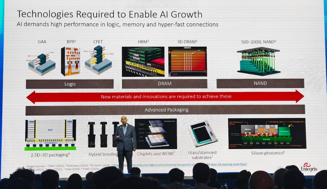
Entegris: Materials Innovation and Advanced Packaging: At the Core of the AI Era
The semiconductor industry is experiencing one of the most profound transformations in its history. Artificial intelligence (AI) has moved from a specialized workload into the center of computing, driving both demand and disruption across the global technology supply chain. At the recent Strategic Materials Conference in Taiwan, the recurring message was clear: while transistor scaling and logic advances remain important, the bottlenecks of the AI era lie elsewhere.System-level performance, interconnect efficiency, and power managementare now the critical determinants of success.
And underpinning all of these areas is a single unifying theme:new materials and materials innovation.
The AI Boom and Its Uneven Benefits
The rise of AI has triggered an unprecedented wave of capital investment. Hyperscalers are now spending between$20 to $25 billion per quarteron infrastructure, a pace that dwarfs previous cycles in cloud and mobile. This massive investment has created extraordinary demand for advanced AI chips, high-bandwidth memory (HBM), and leading-edge packaging.
Yet, when examining the data closely, the benefits of this AI boom are unevenly distributed.
Since 2022, AI semiconductors have shown explosive growth in both sales and wafer demand. However, thenon-AI semiconductor sector has yet to return to its 2022 peak. Today, AI accounts for roughly30% of total semiconductor revenue, but consumes only4.5% of wafer startsat advanced nodes.
This imbalance underscores an important point: while AI is reshaping demand at the top end of the market, much of the broader semiconductor supply chain is still waiting for the benefits to trickle down.
Beyond Scaling: Why Materials Matter More Than Ever
For decades, the industry’s performance roadmap was defined primarily by device scaling. Smaller gate pitches, denser transistors, and improved process design delivered the lion’s share of performance gains. But in today’s environment,materials innovation increasingly has more impact on device performance than simple scaling or design tweaks.
At the device level, the scaling of gate pitch has slowed noticeably since the introduction of FinFET. Performance improvements now come from3D structures, such asGate-All-Around (GAA) nanosheetsandcomplementary FETs (CFETs). Over the next 20 years, we expect to see three major transistor architecture shifts, compared to just one in the previous 45 years. This rapid cadence highlights both the urgency and the complexity of the transition.
Meanwhile, interconnect scaling continues aggressively. Achieving tighter pitches requires new processes likeatomic layer deposition (ALD)andarea selective deposition (ASD), along with entirely new interconnect materials. Copper and tungsten—long the metals of choice—are increasingly challenged by rising resistivity at advanced nodes.
Here,molybdenum (Mo)has emerged as a promising candidate, thanks to its lower resistivity at fine dimensions and reduced barrier requirements. By minimizing the barrier layer fraction, molybdenum allows more volume for actual conductive material, directly improving resistance and reliability.
Three Pathways for Materials Innovation

At the conference, speakers highlightedthree integrated approachesto accelerating materials innovation.
- Module-Level Integration
New materials cannot be considered in isolation; they must be evaluated across the full process module. For example, in chemical-mechanical polishing (CMP), the polish rate, slurry chemistry, post-CMP cleaning, and subsequent etch steps are all interdependent.
By systematically studying the interactions between deposition, CMP, cleaning, and selective etch, engineers can shorten the development cycle and ensure material stability. For molybdenum films, electrochemical analysis and corrosion control were used to identify suitable inhibitors and cleaning chemistries, ensuring long-term reliability.
- Digital and AI-Driven Modeling
Computational chemistry, molecular modeling, and AI search engines are becoming indispensable in material discovery. By simulating reaction pathways, researchers can predict selective deposition behavior before running costly experiments.
One example involved ruthenium precursors, where energy profiles were calculated for different nucleation pathways. The simulations correlated strongly with experimental results, confirming deposition selectivity on titanium nitride while suppressing growth on oxide films. This type ofmodel-driven screeningdramatically accelerates the discovery of viable precursors and inhibitors.
- Virtual Engineering and Additive Manufacturing
Materials innovation also extends to hardware design itself. Usingsimulation-driven additive manufacturing, companies can reimagine components such as gas filters, heat exchangers, and CMP brushes.
By applying biomimicry—for example, mimicking termite mounds for airflow or seed pods for filtration—engineers have achieved200% increases in fuel body volumeand substantial improvements in heat transfer efficiency. These designs would be impossible using conventional manufacturing, but become feasible with computational simulation and 3D printing.
Advanced Packaging: Where Materials and Architecture Converge
While device innovation continues, the biggest changes are happening at thesystem level, particularly in packaging.
2.5D and 3D packagingenable logic and memory to sit side by side on interposers, minimizing latency and maximizing bandwidth.
Hybrid bondingoffers ultra-fine pitch interconnects, critical for chiplet architectures.
Glass and diamond substratesare being explored for better thermal conductivity and mechanical stability.
Silicon photonicspromises to overcome the limits of copper interconnects by enabling optical data transfer directly within packages.
These innovations are not optional; they are essential to support AI’s extreme compute and memory demands. A modern AI training cluster requires tens of terabytes of memory bandwidth and consumes megawatts of power. Without advanced packaging and novel substrates, such systems would be infeasible.
The Power and Thermal Wall
The march toward exascale and zettascale AI is colliding with two fundamental barriers:power consumption and heat dissipation.
NVIDIA’s latest GPUs already consume700–1,000 watts each, with future products projected at multiple kilowatts per GPU. System-level power draw is moving from tens of megawatts toward hundreds of megawatts—comparable to entire power plants.
This creates enormous challenges for materials, cooling, and infrastructure:
Newthermal interface materialsanddiamond substratesare being tested to improve heat spreading.
Liquid coolingis transitioning from optional to mandatory in high-density racks.
Future systems may requirephotonic interconnectsto reduce both power and thermal overhead from copper signaling.
In other words, solving the thermal wall is as important as solving the compute wall.
The Economics of AI and Semiconductor Growth
Even as AI surges, the industry must remain cautious. Today’s massive hyperscaler capex is directed toward a relatively narrow slice of the supply chain—AI accelerators and HBM. Many other segments, from consumer electronics to automotive MCUs, are still struggling to regain pre-2022 momentum.
The challenge for the broader semiconductor ecosystem is totranslate AI-driven investment into industry-wide benefits. This will require closer coordination across foundries, OSATs, equipment makers, and material suppliers.
The Next Decade of Materials-Driven Scaling
Looking forward, three key trends are likely to define the next decade:
Logic Transformation
From GAA to CFET, logic devices will undergo more architectural changes in the next 20 years than in the previous 40. Materials innovation at the contact and channel level will determine performance and power efficiency.
Memory Expansion
HBM, 3D DRAM, and 1,000-layer NAND will provide the storage and bandwidth AI requires. But these advances will demand new etching chemistries, dielectrics, and ultra-low-defect materials.
System-Level Innovation
Advanced packaging, photonics, and hybrid bonding will enable heterogeneous integration. The shift from PCB-level to package-level interconnect will redefine system design, with materials science as the enabler.
AI has redefined the priorities of the semiconductor industry. The old model—focusing narrowly on transistor scaling—is no longer enough. Instead, the future belongs to those who can integratedevice scaling, new materials, advanced memory, and disruptive packaginginto coherent systems.
Materials are no longer the silent enablers at the bottom of the stack; they are nowstrategic differentiatorsthat shape performance, efficiency, and scalability. The winners of the AI era will be those who master the interplay betweenmaterials science, device innovation, and system architecture.
Just as the introduction of FinFET once redefined a generation of logic, the coming wave of materials breakthroughs—from molybdenum interconnects to diamond substrates and silicon photonics—will redefine the future of AI hardware. The industry stands at the threshold of a new paradigm:a materials-driven Moore’s Law for the AI age.

AGC: Integrating Glass Solution in Advanced Packaging
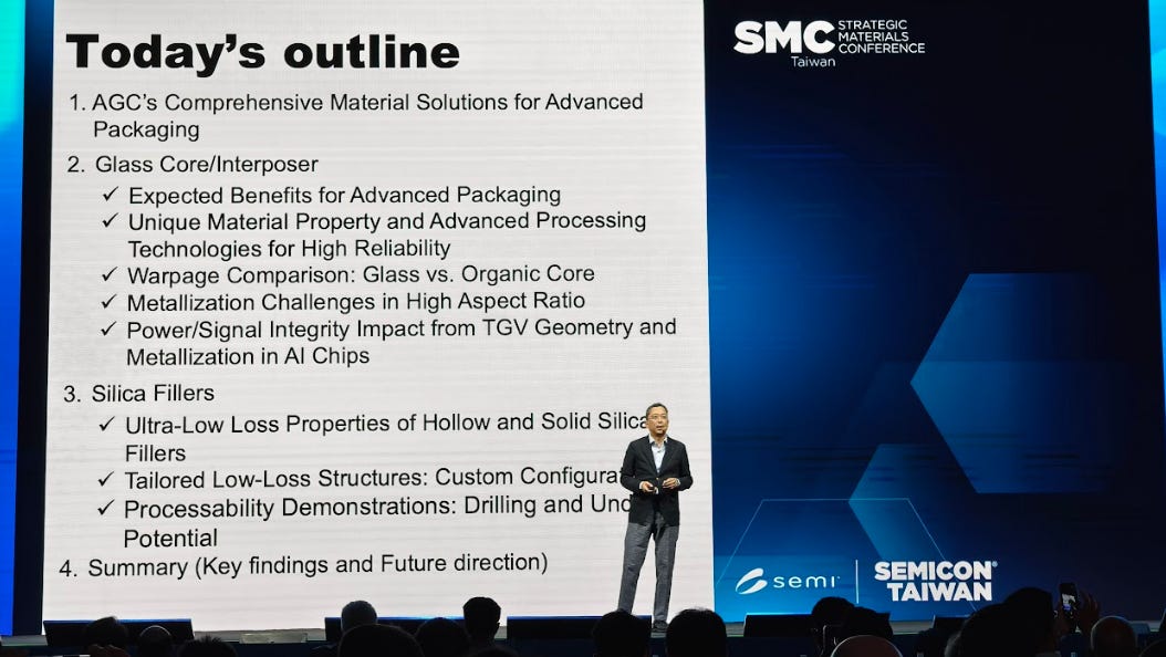
AGC’s Broad Semiconductor Contributions

AGC’s footprint spans a wide set of semiconductor applications:
FEOL Contributions:
EUV photomask blanksandsynthetic quartz glass, both in mass production.
SiC ceramicsfor high-purity, low-expansion heat treatment jigs.
BEOL Contributions:
CMP slurriesdesigned to match advanced design rules.
Glass Core substrateswith fine via pitch using TGV.
Carrier glasswith tailored coefficients of thermal expansion (CTE) to suppress warpage in heterogeneous integration.
Build-up filmsandcopper clad laminates (CCL)with ultra-low dielectric constant (Dk) and loss tangent (Df).
Silica fillers(hollow for low Dk, solid for low Df) in both industrial and semiconductor development.
Beyond these, AGC developslow-dielectric adhesives,polymer optical waveguides,low-temperature soldering materials, andglass-ceramics substratesfor high-brightness LEDs and semiconductor lasers. This diversified portfolio supports applications fromfan-out packaging and interposerstooptical interconnectsfor Co-Packaged Optics (CPO).
The Developmental Path of Glass Core Technology
AGC began pursuing TGV technologies in collaboration with Georgia Tech around 2010, aiming to reduce the cost of silicon interposers. Over the following decade, AGC built a robust roadmap:
2012–2017:Expansion from 6"/8"/12" wafers to large-format glass substrates, targeting interposer and RDL packaging.
2017–2020:Applications extended to RF devices such asIPD, FWA, and AiP, driving demand for TGV in 5G infrastructure.
2020–2025:Mastery of high-speed drilling, enabling high aspect ratio (AR=20) vias for glass >1 mm thick.
2025–2035 Roadmap:
Adoption of glass cores for chiplet packaging in data center AI.
Integration of optical interconnects forCo-Packaged Optics.
By 2050, a vision of1 Tb/s photonics systemscombining photonic ICs, glass optical waveguides, and polymer waveguides.
AGC’s long-term roadmap reflects the shift fromelectrical interconnectstoelectrical + optical hybrids, enabling higher frequencies, lower losses, and integration with photonics.
Key Properties of Glass for Packaging

Glass is uniquely adaptable due to its tunable composition and structure. AGC leverages its material expertise to optimize:
CTE Variability:Allowing substrate designers to balance stress and structural integrity.
Dielectric Performance:Low-loss glass options outperform conventional CCL, essential for high-frequency and mmWave.
Surface & Thickness Control:AchievingTGV precision down to 20 μmandTTV <1 μmfor photonic-grade substrates.
Mechanical Strength:Tailoring Young’s modulus and minimizing warpage.
Examples includeEN-A1andsynthetic quartz AQ, suitable for 5G chip substrates requiring high TGV precision, with even stricter demands at >80 GHz and photonic applications.
Through Glass Via (TGV) and Metallization Challenges
TGV is the backbone of glass-core substrates. AGC optimizesvia shapes—straight, tapered, or X-shaped—depending on application. Yet, the true complexity lies inmetallization, where glass presents unique challenges:
Ensuringseed layer step coverage.
Achievingadhesion >4 N/cmbetween copper and glass.
Preventingvoids, recesses, and cracks.
Maintaininguniform Cu thicknessandCMP planarity.
AGC has demonstrated strong results withelectroless Cu plating, achieving85% step coverageand5.3 N/cm peel strengthon thick glass substrates. The company is now establishingProcesses of Record (PORs)that integrate glass composition, drilling, metallization, and inspection to de-risk adoption for substrate manufacturers.
Reliability Testing and HVM Considerations
To enable high-volume manufacturing (HVM), AGC subjects glass substrates to stringentJEDEC reliability tests:
Temperature humidity soak (85°C/85% RH).
High/low temperature storage (-55°C to 150°C).
Temperature cycling (200 cycles).
BHAST with electrical bias.
Solder reflow stress.
These tests ensure robustness under real-world conditions, but reliability is strongly affected by interdependencies between glass type, seed layer, plating process, and downstream thermal excursions. AGC’s emphasis on unified PORs reflects its focus onyield optimization and total cost of ownership.
Strategic Outlook: Glass as a Platform for AI and Beyond
The applications of glass core substrates are increasingly tied toAI data centers, high-performance computing (HPC), 5G/mmWave RF, and optical interconnects. By offering low-loss, high-precision, and hybrid-compatible substrates, AGC positions glass as the natural successor to organic substrates and even silicon interposers.
In the near term,chiplet packagingandRF AiPwill drive adoption. By the 2030s,Co-Packaged Opticsand hybrid electron-photon integration will define glass’s role in HPC and networking. Long-term, glass substrates may enable the industry’s transition fromelectrons to photons, supporting terabit-scale interconnects.
AGC’s presentation at SEMICON underscored howglass materials are becoming central to semiconductor packaging innovation. By combining a century of materials expertise with a forward-looking roadmap, AGC is addressing the dual challenges ofscaling complexityandsystem-level performance.
The company’s vision is clear: glass is not simply another material option, but aplatform technologyenabling chiplets, advanced RF, and photonics integration. Success will depend not only on solving technical hurdles—like TGV metallization—but also on ensuring manufacturability, reliability, and cost-effectiveness.
As the industry enters the AI era, AGC’s glass technologies may prove to be a cornerstone, bridging today’s packaging limitations with tomorrow’s photonic future.
If readers would like to learn more about the key takeaways from the Semicon Taiwan technical forums, SemiVision has compiled a related report. Please feel free to reach out to us at: jett@semivisiontw.com & eddyt@semivisiontw.com


PreviousNext
TopLatestDiscussions








See all