Lightmatter Passage : A 3D Photonic Interposer for AI
Lightmatter Passage : A 3D Photonic Interposer for AI
- Source: SemiVision
- Author: SEMIVISION
- Published: 2025-09-12T17:41:17+08:00
- URL: https://tspasemiconductor.substack.com/p/lightmatter-passage-a-comprehensive Lightmatter Passage : A 3D Photonic Interposer for AI


Lightmatter Passage : A 3D Photonic Interposer for AI
Original Article by SemiVision Research (TSMC , Nvidia , Lightmatter )

Sep 12, 2025
∙ Paid
Scale-Up Challenges in Modern AI Training
Technical Background and Challenges
Over the past decade, the scale of AI models and their computational demands have grown exponentially—from early models with only a few million parameters to today’s models with hundreds of billions or even trillions. For instance, training large language models such as GPT-3 and GPT-4 typically requires thousands of GPUs in scale-out distributed systems to complete within a reasonable time. However, this expansion approach faces significant challenges.

2025年2月19日
On one hand, the slowdown of Moore’s Law has limited improvements in single-chip performance. On the other hand, multi-node distributed training introduces massive data communication overhead and synchronization delays, making network bandwidth a critical bottleneck. NVIDIA CEO Jensen Huang has noted that the computational demand for the latest AI training and inference workloads has surged by as much as 100x compared to expectations just a year earlier.
As a result, modern large-scale AI training is caught in a dilemma betweenScale-Up(maximizing single-node performance) andScale-Out(expanding horizontally across many nodes). Relying solely on massive GPU clusters leads to severe networking bottlenecks and soaring power consumption, while depending on single-node performance gains runs into limits of semiconductor scaling, thermal management, and power density.
Overall, in the post-Moore’s Law era, overcoming the dual bottlenecks of compute and communication has become a shared challenge for the entire industry.
Passage Technology Details
Lightmatter has identified that today’s primary bottleneck lies in insufficient interconnect capabilities across chips. To address this, the company introduced thePassage M1000 “superchip” platform, built on photonic technology to overcome critical Scale-Up barriers. The Passage M1000 employs an innovative3D photonic stacking architecture, integrating up to34 chipletson a single photonic interposer, with a total equivalent die area reaching4,000 mm²—surpassing the traditional reticle limit of a single chip.
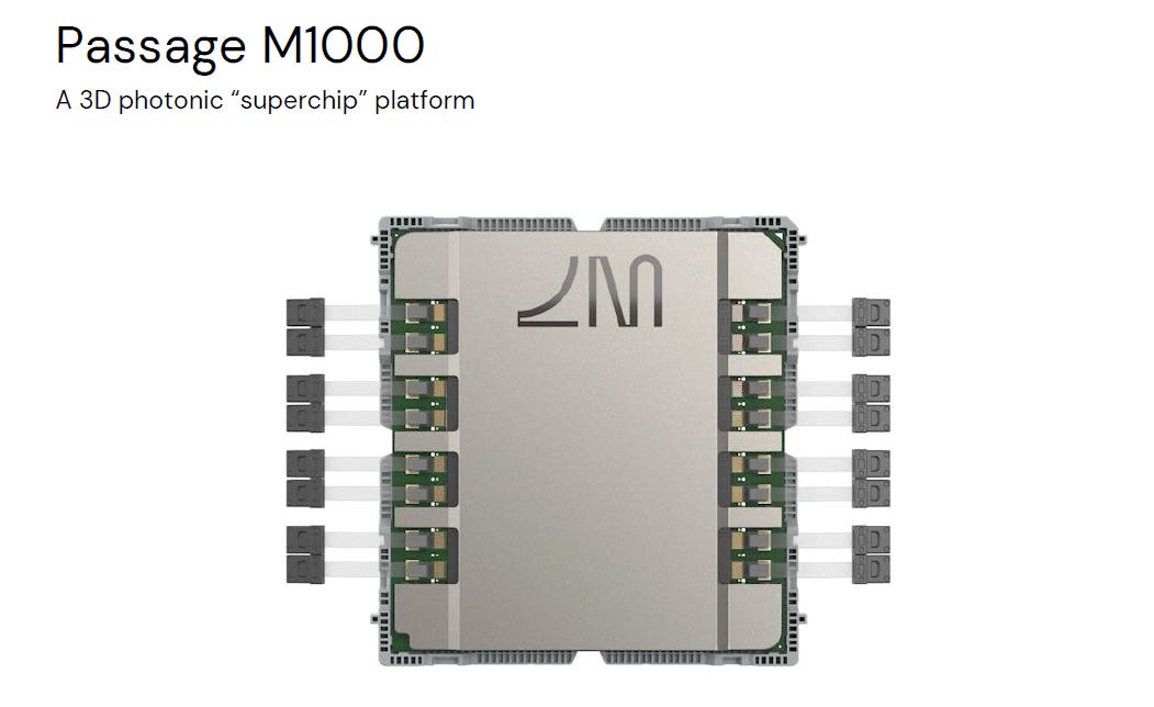
This approach enables the Passage platform to deliver unprecedented interconnect bandwidth:114 Tbps of total bidirectional bandwidth (Tx+Rx)and1,024 high-speed SerDes lanes. This means each integrated compute chiplet can access multi-terabit-per-second I/O bandwidth, effectively breaking through the conventional bottleneck of periphery-limited I/O pins on monolithic chips. As Lightmatter’s presentation put it:“We need more than 100× the bandwidth; a new paradigm is imperative.”
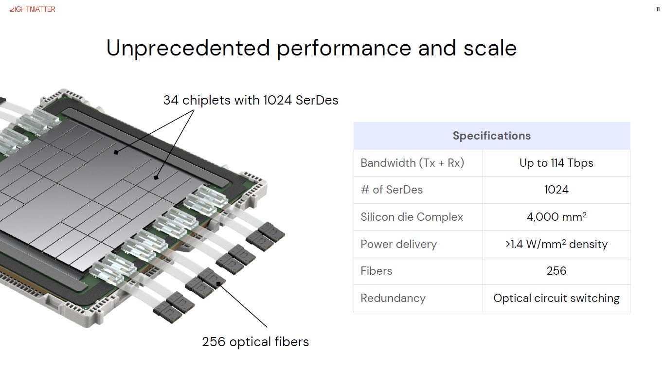
By leveraging its photonic stack, Passage allows numerous chiplets to share a high-speed optical communication backplane, collaborating with near-monolithic efficiency. This represents a new path forward in tackling modern AI Scale-Up challenges.
Photonics AI Processor in Nature: A Comparative View
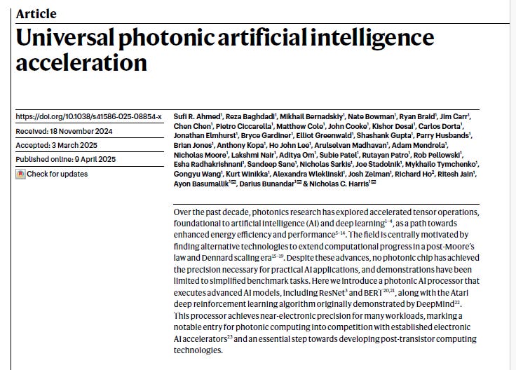
A paper published inNaturevalidated the feasibility of photonics for AI acceleration from another perspective. The study showcased thefirst photonic processor capable of executing advanced neural networkssuch as ResNet and BERT, achieving accuracy close to that of 32-bit floating-point digital accelerators across multiple complex tasks.
This photonic processor employed amulti-chip integrated package, vertically combiningsix chips within a single package(four 128×128 photonic tensor cores, PTCs, plus two 12nm digital control interfaces, DCIs). High-speed interfaces connected the photonic compute chips with the electronic control chips, boosting system integration and computational efficiency.
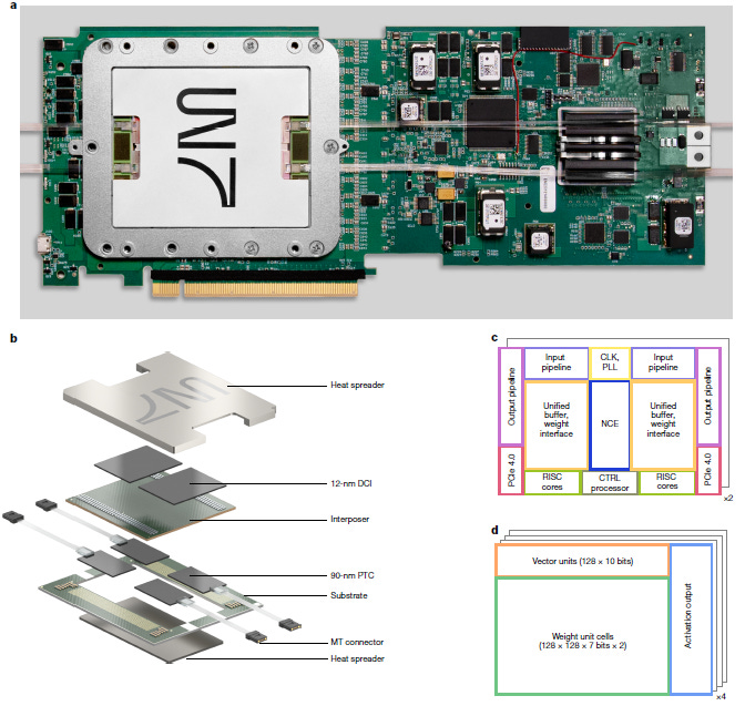
The design demonstrated that high-density packaging and vertical opto-electronic interconnects can significantly improve energy efficiency without sacrificing accuracy. In testing, the processor achieved65.5 trillion 16-bit operations per second, consuming only ~78 W of electrical power plus 1.6 W of optical power. TheNaturepaper described its performance across workloads as achieving“near-electronic accuracy,”marking an important step toward the practical adoption of photonic computing in the post-Moore’s Law era.
Compared with Lightmatter’s Passage—which focuses oncross-chip interconnect—theNaturephotonic processor emphasizestensor computation at the photonic core level. Yet both approaches highlight photonics’ potential under Scale-Up challenges: the former offers a revolutionary data transfer architecture, while the latter proves that photonic compute cores can compete with electronic accelerators. Together, they suggest a future wherephotonic interconnect networks link multiple photonic/electronic compute cores, forming a new class of AI supercomputing platforms.
Comparison with Other Industry Players
As AI training continues to scale, other major players in the industry have taken different approaches to address the Scale-Up challenge:
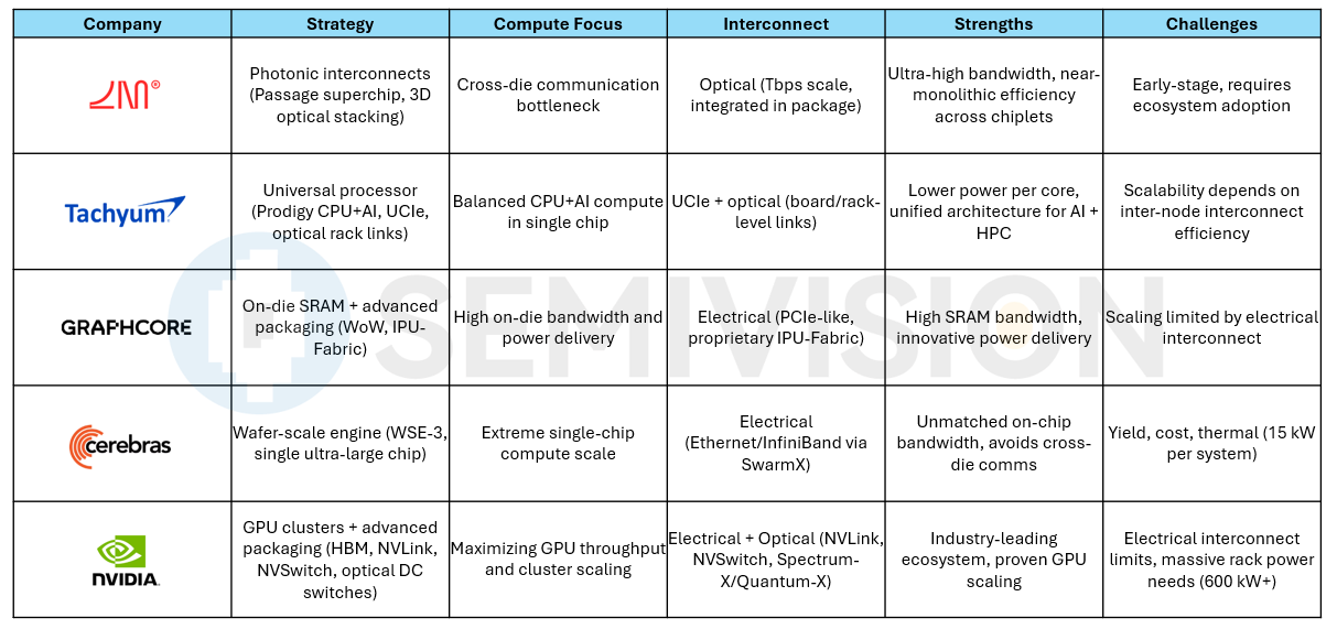
NVIDIA: NVIDIA has continued along a path of GPU cluster expansion coupled with advanced packaging. Its latest-generationBlackwell Ultra GPUadopts a dual-die design with208 billion transistors, delivering roughly50% higher performancethan its predecessor, the H100.
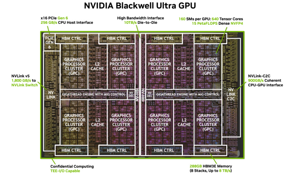
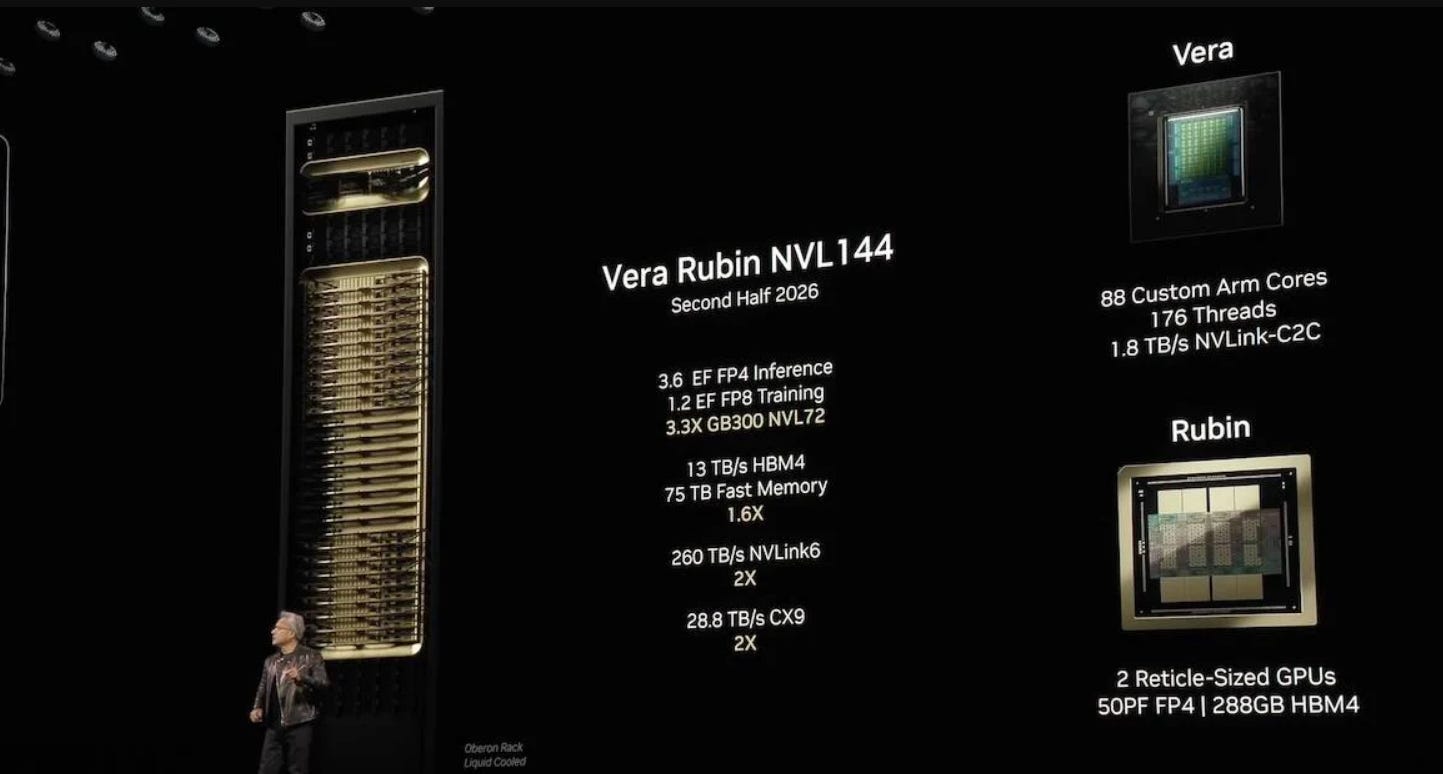
NVIDIA also plans to introduce theVera Rubin superchipin 2025–2026, which will combine the next-generation “Rubin” GPU and “Vera” CPU. Built on a3nm processand paired withHBM4 memory(offering13 Tbps bandwidth, a major leap from the H100’s HBM3E at 8 Tbps), the Rubin GPU will deliver50 PFLOPS (4-bit) inference peak performance, about2.5× the Blackwell architecture. The follow-upRubin Ultra, essentially packaging two Rubin GPUs together, is projected to reach100 PFLOPS FP4 performancewith nearly1 TB of unified memory.

To support such massive compute power, NVIDIA is upgrading its interconnect technologies: the next-generationNVLink 6point-to-point interface provides up to3.6 Tbps total bandwidth per node. At the same time, NVIDIA is rolling out photonics-based datacenter switches (e.g.,Spectrum-X, Quantum-X) offering port speeds up to800 Gbps, capable of linking millions of GPUs.


2025年6月17日
Overall, NVIDIA continues to rely on powerful chip stacking (e.g., multi-chip modules combining Grace CPUs with Hopper GPUs),high-bandwidth HBM memory, and improvedelectrical interconnects (NVLink/NVSwitch)to achieve leading performance. However, thepower and distance limitations of electrical interconnectsare becoming increasingly prominent, requiring massive rack-scale and network infrastructure (with a single Vera Rubin rack consuming as much as600 kW) to scale compute.
By contrast,Lightmatter’s Passagepursues optical interconnect to achievetens to hundreds of Tbps networking capability within a single machine, effectively collapsing datacenter-level communication into a “superchip.” This architectural path holds the potential to simplify AI factory-style deployments and significantly improve efficiency.
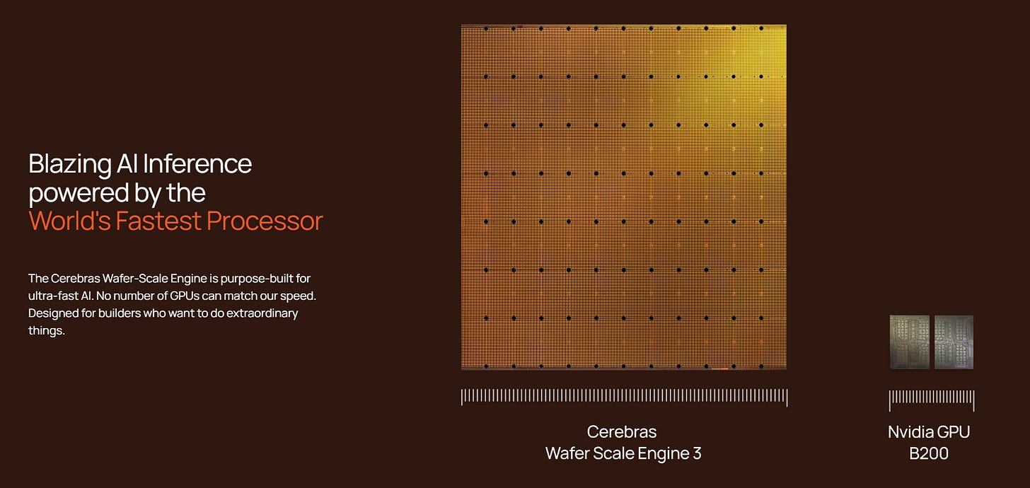
Cerebras: Cerebras has taken an extremeScale-Upstrategy by building theWafer-Scale Engine (WSE), a single chip covering the entire wafer with a die area of46,250 mm². The latest third-generationWSE-3packs4 trillion transistors,900,000 sparse linear algebra cores, and integrates42 GB of on-chip SRAMwith an astonishing21 PB/s of on-chip memory bandwidth.
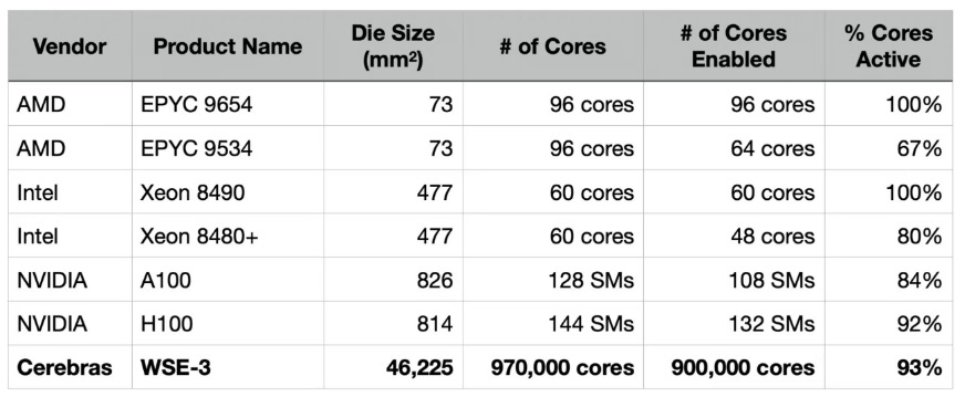
Such massive on-chip compute resources allow the WSE to train ultra-large modelswithout requiring cross-chip communication. For example, the WSE-3 can fit the full weights of a24-trillion-parameter modelentirely within a single chip, with all data access occurring in a unified logical memory space. This delivers extremely high internal bandwidth density (21 PBytes/s—about 7,000× that of a conventional NVIDIA H100 GPU) and ultra-low latency, fundamentally different from multi-GPU clusters constrained by inter-node communication.
However, wafer-scale engines face challenges inmanufacturing yield, thermal management, and cost. A singleCerebras CS-3 system consumes up to 15 kW, and its economies of scale lag behind standard GPUs. Cerebras is currently promoting its cluster solution, linking thousands of WSEs viaSwarmX interconnectto build supercomputers. Yet, since scaling beyond a single wafer still relies onexternal high-end Ethernet/InfiniBand linksrather than optical interconnects, and given the high overall cost, the approach faces hurdles.
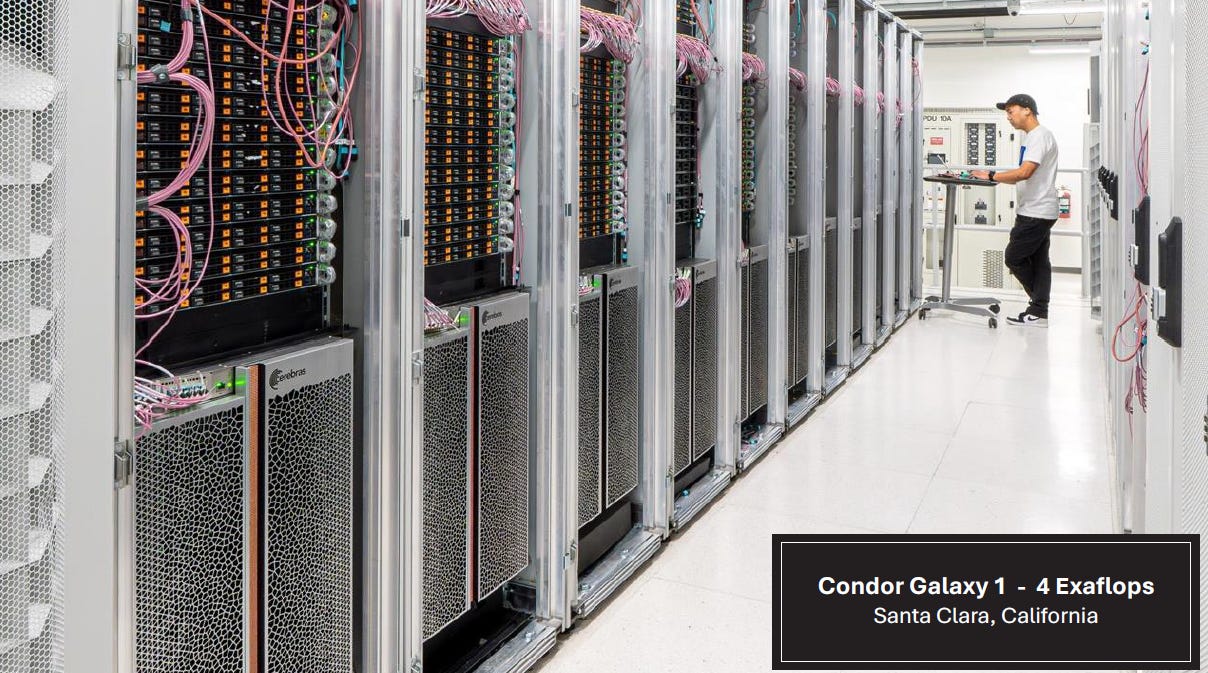
By contrast,Lightmatter’s Passage, while not offering the same per-chip compute power as WSE, leveragesoptical interconnectsto enable near-monolithic bandwidth communication across standard chiplets. This provides an alternative compromise: achievinggiant-chip-like performanceby tightly connecting smaller dies with dense optical links, potentially offering bettercost efficiency and flexibility.
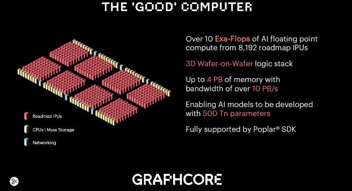
Graphcore: UK-based Graphcore focuses on innovations in advanced packaging and memory architectures. Its second-generationIPU (Colossus MK2)integrates900 MB of distributed SRAM, delivering up to260 TB/s of on-chip memory bandwidththrough near-memory design.

In 2022, Graphcore introduced theBow IPU, which adopted TSMC’sWafer-on-Wafer (WoW) 3D stacking technology. It directly bonded a compute wafer containing1,472 AI coreswith a passive power-delivery wafer. This innovative packaging enabled the Bow IPU to operate at1.85 GHz(vs. 1.35 GHz in the prior generation) at lower voltage, resulting in a~40% performance boostand16% improvement in energy efficiency. The principle lies in integrating deep trench capacitors and vertical TSVs within the power-delivery wafer, which supply stable power close to the compute cores, allowing higher clock speeds without increasing power consumption.
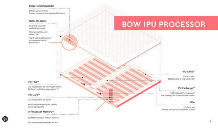
Graphcore’s architectural strength is that each IPU integrates large on-chip memory and thousands of small parallel cores, making it well-suited for models requiring extremely high memory bandwidth. Additionally, Graphcore provides its proprietaryIPU-Fabric interconnect, enabling multiple IPUs to form Pod systems. However, communication between IPUs still relies on electrical interfaces (similar to PCIe or proprietary links), which becomes less efficient at very large scales (hundreds of chips or more) compared to optical interconnect solutions.

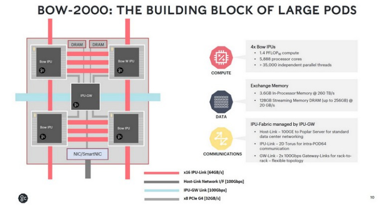
By contrast,Lightmatter’s Passagefocuses on breaking thecross-die communication bottleneck, whereas Graphcore emphasizeson-die bandwidth and power delivery improvements through packaging innovation. In the future, combining Graphcore’shigh-bandwidth on-chip SRAM designwith Lightmatter’schip-to-chip optical interconnectcould potentially unlock even greater performance for distributed AI computing.
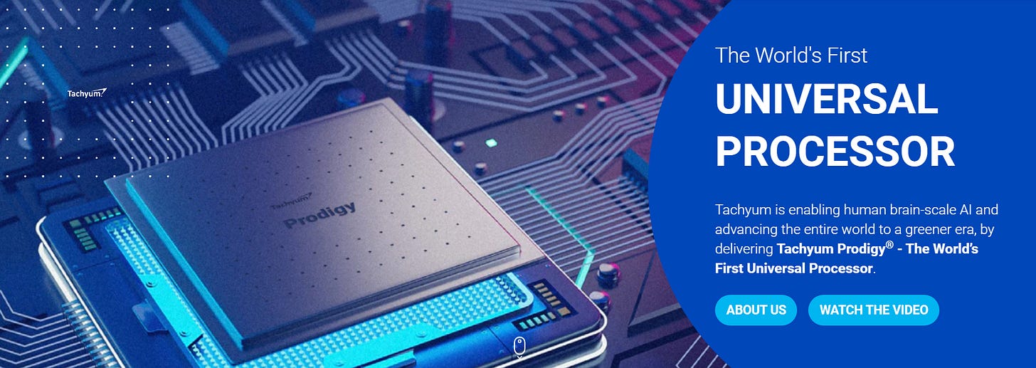
Tachyum: Tachyum is pursuing the“universal processor”route, aiming to create a new CPU architecture capable of handling both traditional HPC and AI workloads. Its upcomingProdigy chipadopts an advanced multi-core design, reportedly offering up to192 64-bit cores, with AI computing performance comparable to GPUs, while delivering better compute density and power efficiency.
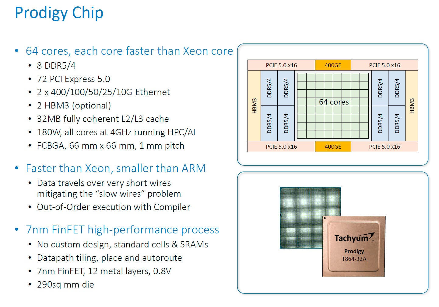
Tachyum emphasizes that its cores consumean order of magnitude less powerthan conventional processors, while supporting a unified architecture that can handle inference, training, and general-purpose computing tasks simultaneously. On the interconnect side, Tachyum has embraced theUCIe open chiplet interconnect standard, enabling future chiplet-based functional module expansion.
In addition, Tachyum is collaborating with optical connector vendors to introduceadvanced fiber-optic high-speed connectivityinto its Prodigy systems (e.g., co-developing OSFP-compatible optical modules withSenko) to enhance node-to-node communication bandwidth.
Compared with NVIDIA’s specialized accelerators, Tachyum’s strategy is to deliverbalanced CPU + AI performance within a single chip, reducing data movement between heterogeneous devices. However, forultra-large model training, Tachyum will still require clusters of multiple Prodigy chips, makinginter-node interconnects a key determinant of scalability.
Tachyum’s focus on optical interconnects underscores its recognition of the limitations of traditional electrical links—an idea aligned withLightmatter Passage’s philosophy of breaking communication bottlenecks through photonics. That said, Tachyum’s optical connectivity approach remains oriented towardboard- or rack-level interconnect improvements, whereas Passage integrates optics directly into thepackage-level interconnect fabric, potentially achieving far greaterintegration depth and bandwidth density.
Analysis and Conclusion
Looking across the various approaches, the paths to scaling compute can be broadly divided into two categories:“building more powerful units”and“connecting more units more tightly.”NVIDIA, Graphcore, and Tachyum lean toward the former, using advanced process nodes, multi-die packaging, and architectural optimizations to create increasingly powerful compute units; Cerebras takes this to the extreme by delivering maximum performance on a single ultra-large chip.
However, as per-unit performance rises,data movement has become the bottleneck, prompting companies to also pursue the latter path: adopting faster electrical interfaces and even experimenting with optical interconnects.Lightmatter’s Passageexemplifies this trend, centering on3D photonic interconnectsto tackle the long-overlooked cross-die communication challenge, standing out among the many approaches to scaling compute. Compared with traditional electrical interfaces, Passage can deliverhundreds of Tbps of interconnect bandwidth at reasonable power, allowing horizontally scaled systems to operate almost as efficiently as scaling up a single giant chip.
Meanwhile, theNature photonic AI processorprovides validation from another angle, demonstrating that photonics can be used not only for communication but also for executing core arithmetic operations—with accuracy and energy efficiency competitive with electronic solutions. These advances complement each other and suggest a paradigm shift in AI acceleration: moving beyond sole reliance on transistor scaling, towardhybrid electronic-photonic architecturesthat break through performance ceilings.
In conclusion, under the Scale-Up challenges of modern AI training, a diversity of innovative approaches is flourishing. The emergence ofLightmatter Passageoffers the industry a breakthrough pathway, delivering leapfrog improvements from the interconnect layer.
For Paid Member, SemiVision will discuss topics on:
Understanding Scale-Out vs. Scale-Up Computing
Distance Limitations of Copper Interconnects and Power Density Challenges
Passage 3D Photonic Stacking Solution Explained
UCIe and Interface Protocols
Packaging Technologies
Breakthroughs in Bandwidth Density and Energy Efficiency
Lightmatter Passage M1000: A Photonic Interconnect “Superchip”
Understanding Scale-Out vs. Scale-Up Computing
Technical Background and Challenges
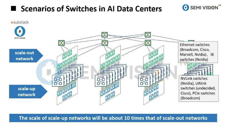
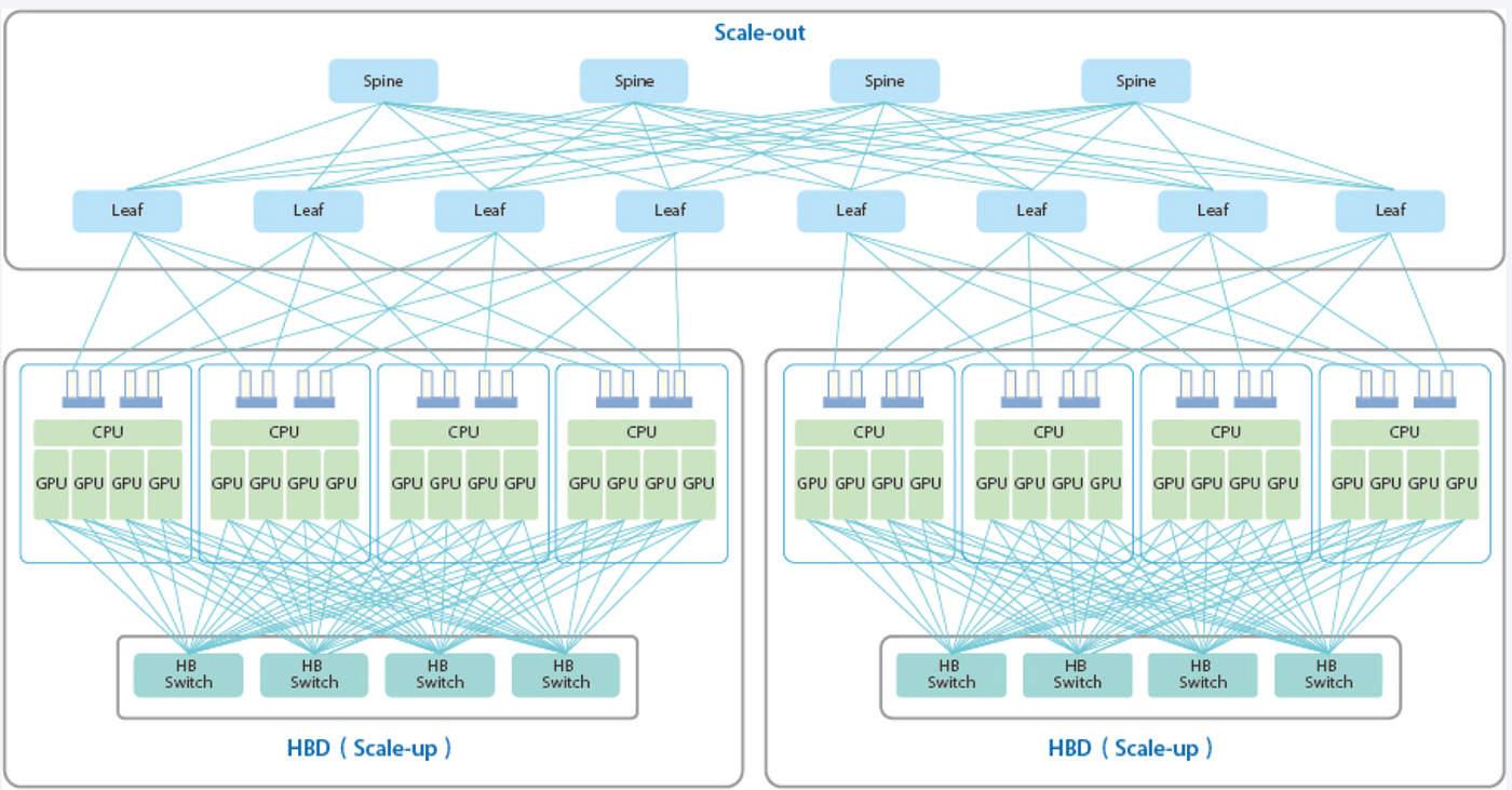
When discussing compute scaling, two models are often mentioned:Scale-OutandScale-Up.
Scale-Outrefers to expanding overall compute power by adding more nodes—for example, deploying additional servers or GPUs to share workloads.
Scale-Upmeans increasing the maximum compute capability within a single node, such as using more powerful processors or integrating multiple compute dies into one package.

Source: GF
Traditionally, deep learning training has relied heavily on Scale-Out: as model and dataset sizes grow, parallel deployment across multiple GPUs is the relatively straightforward solution. However, the communication overhead of Scale-Out rises non-linearly with node count—the more nodes involved, the greater the proportion of each training cycle spent on parameter synchronization and data exchange. This leads to diminishing efficiency in scaling performance. Furthermore, since memory across nodes is disaggregated, gradient and parameter updates must traverse the network, which is constrained by bandwidth and latency. For very large models (e.g., those requiring model parallelism or Mixture-of-Experts, MoE), communication latency often becomes the training bottleneck.
By contrast,Scale-Upstrengthens the capacity of a single node, thereby reducing frequent cross-node communication. In theory, the ideal form of Scale-Up is to keep the entire training workload within a single compute resource, so that all data access occurs locally. Yet achieving extreme Scale-Up is not straightforward.
First, manufacturing ultra-large chips faces yield and cost challenges: the larger a die, the higher the probability of defects, leading to steep drops in usable yield. Second, power and thermal constraints impose hard limits; the power and cooling capacity a single package can handle is finite. For instance, typical GPUs already exceed 300W, while high-end processors like NVIDIA’s GH200 (Grace+Hopper) CPU/GPU integration require custom cooling solutions. Third, a single chip’s I/O pins and package footprint are limited, making it difficult to simultaneously provide sufficient memory bandwidth and network connectivity. While compute capability scales with chip area, I/O bandwidth grows only with chip perimeter. This discrepancy often results in the“shoreline bottleneck”: the larger the die, the more insufficient the periphery I/O resources become relative to the compute core.

Passage Technical Details
The original design goal of theLightmatter Passageplatform is to overcome the so-called shoreline bottleneck by leveraging 3D photonic stacking to achieve an effect that appears like Scale-Out but in practice behaves like Scale-Up.
ThePassage M1000, described as a 3D photonic “superchip,” integrates many smaller compute chiplets onto a single photonic interposer. This effectively builds a massive, tightly interconnected logical device. The architecture combines the advantages of both Scale-Out and Scale-Up:
On one hand, modular chiplets provide yield benefits and manufacturing flexibility (similar to composable Scale-Out expansion).
On the other, ultra-high-bandwidth photonic interconnects allow the system to function as if it were one monolithic die (achieving Scale-Up–style tight coupling).
Specifically, the Passage M1000 employs a2×4 tile structure, with 8 photonic interconnect modules tiled together to form the superchip. Each tile integrates16 horizontal optical buses, and each bus supportstwo full-duplex optical links. Every optical link uses8 wavelengths (λ) × 56 Gbps/λvia wavelength-division multiplexing (WDM), delivering up to448 Gbps per link. In other words, each optical bus approaches~1 Tbps aggregate throughput, resulting in immense bandwidth per tile.
These optical buses enable high-speed communication among chiplets within the same tile, while also extending across tile boundaries: each transmitter (TX) group can send signals to adjacent tile receivers (RX), or vertically couple signals off-chip. Conversely, each RX group can accept signals from neighboring tiles or external fibers. This mechanism creates adynamically reconfigurable optical communication fabric.
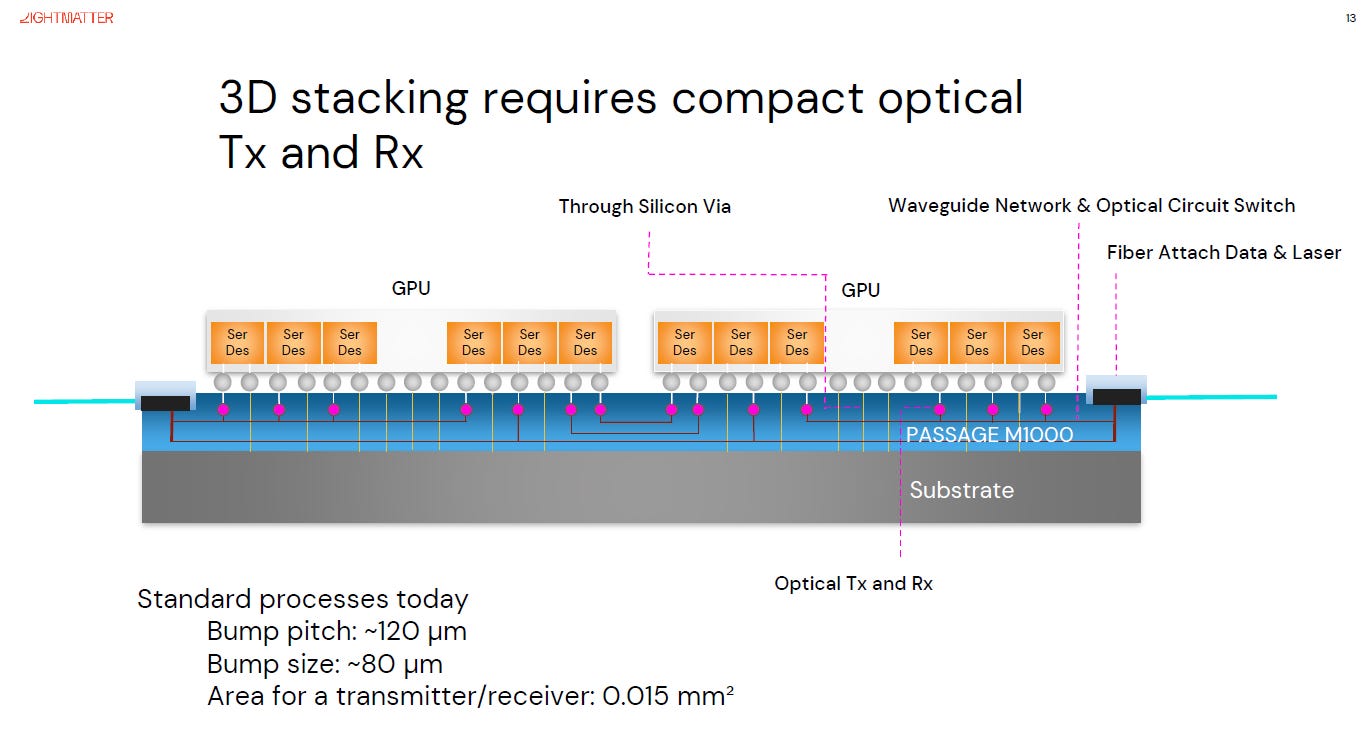
The photonic interposer also integrates anoptical circuit switch, which can programmably alter the connectivity among waveguides. This allows the overall topology of the superchip to be adapted on demand—for example, switching communication modes between different training tasks or rerouting traffic in the event of optical path failures—thus improving system fault tolerance.
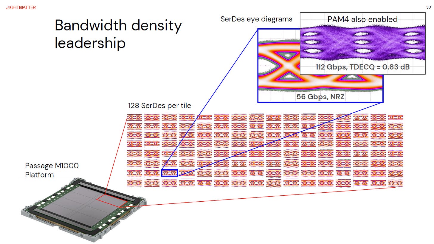
Thanks to compact optical devices such asmicroring modulators(see later discussion), the Passage platform achieves extremely high I/O density: each tile includes128 high-speed SerDes channelsto drive microring optical transceivers. Across the entire M1000, this scales to1,024 SerDes channels distributed over 34 chiplets. Such density would be nearly impossible for traditional electrical I/O at package edges, but Passage bypasses planar constraints through 3D-stacked vertical photonic coupling.
In total,34 compute chiplets(GPU, accelerator, or other ASICs) are tightly bound together by the photonic interposer, which itself connects externally through256 optical fibers. Although the fiber count sounds daunting, Lightmatter usespluggable fiber couplersthat align fiber arrays to on-interposer waveguides, and each fiber supports bidirectional multi-wavelength transmission—significantly boosting per-connection efficiency.
Taken together, thePassage M1000 condenses the communication demands of dozens or even hundreds of modules in a conventional Scale-Out environment into a single Scale-Up super-package. It realizes the long-sought ideal:compute within the chip, and communication as if within the chip.
Comparison with the Photonic AI Processor inNature
The photonic processor experiment reported inNaturealso demonstrates the concept of multi-chip vertical integration, but its purpose and scale differ from that of Passage.

In theNaturephotonic accelerator package,four Photonic Tensor Cores (PTCs)are stacked beneathtwo Digital Control Interface (DCI) chips. Each PTC die measures roughly14 × 25 mm, fabricated in GlobalFoundries’90 nm photonics process, and integrates microring modulator arrays, photodiodes, and other analog optical computing elements. The DCI, by contrast, is fabricated in GlobalFoundries’12 nm process, sized31.4 × 25.0 mm, and incorporates64 RISC-V processors and 268 MB of cachefor control and storage functions.
The package employs a large54 × 56 mm organic interposer: the DCI chips are mounted on top, while the four PTCs are vertically aligned beneath them and interconnected through the interposer. Although the paper does not detail the wiring, it can be inferred thatdense microbumps and through-silicon vias (TSVs)carry both analog and digital signals between the PTCs and DCIs, creating a tightly coupled compute-control stack. This type of vertical 3D packaging is conceptually similar to Passage’s photonic interposer in that both shorten interconnect distances by stacking functionally diverse dies.
However, the role of photonics differs fundamentally. In theNaturedesign, optics perform thecomputation itself: the PTC executes matrix multiplications (multiply-accumulate) in the analog domain using microring modulators, while the DCI digitizes the results with high-speed ADCs and carries out further digital processing. In contrast, in Lightmatter’sPassage, optics are primarily used forcommunication—transmitting electrical signals converted into light across chiplets and modules—while compute remains on conventional electronic dies.
These architectural differences highlight divergent priorities:
TheNaturephotonic processor aims to boostcompute efficiency and energy performance within a single module.
Passage focuses oncommunication efficiency and scalability across many modules, enabling system-level expansion.
It is worth noting that theNatureprocessor still confronts multi-chip integration challenges. In total,six chipswere integrated into a single accelerator, with researchers addressing power delivery and thermal issues by attaching a heatsink and capping each photonic core’s power at the10 W levelto enable integration.
Overall, theNaturephotonic AI chip demonstrates that by combining photonic computing elements with 3D packaging, tasks previously requiring multiple GPUs can be executed within a single node. But it does not provide Passage-like networking capabilities to scale across nodes—the four PTCs are confined to one accelerator card and cannot directly optically connect to another card. By contrast, Passage establishes aphotonic interconnect fabric for multi-node systems, extending optical communication hundreds of meters beyond the package, effectively delivering Scale-Up-like connectivity to Scale-Out deployments.
Thus, the two approaches can be viewed as complementary: one enhancesintra-module compute performance, while the other extendsinter-module communication bandwidth—both leveraging 3D optoelectronic integration to break past traditional limits.
Comparison with Other Industry Approaches
The traditional boundary betweenScale-OutandScale-Upis becoming increasingly blurred as new technologies emerge, with each company pursuing hybrid strategies:
NVIDIA Grace Hopper / DGX:
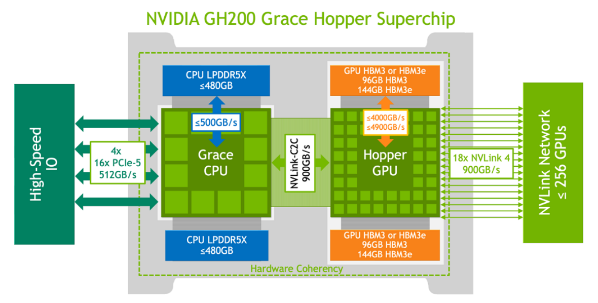
NVIDIA’s latestGH200 “Grace Hopper”tightly couples a CPU (Grace) with a GPU (Hopper) via a silicon interposer, using theNVLink-C2C interfaceto achieve900 GB/s bidirectional CPU–GPU bandwidth, enabling near-monolithic sharing of up to600 GB of memory. This is a form of 2.5D multi-die integration, bringing heterogeneous components closer together to boost single-node performance in a Scale-Up manner.
At the system level, theDGXplatform leveragesNVSwitchto form a fully connected topology of eight GPUs, where each GPU has equal-length, high-speed links to every other GPU. This reduces latency and maximizes bandwidth within a small cluster (e.g., the DGX-2 achieved300 GB/s GPU–GPU interconnect). However, beyond a single chassis, scaling still depends on InfiniBand networks, where performance is limited by lower inter-node bandwidth (e.g., the latest 800G InfiniBand ports provide only ~200 Gbps unidirectional).
Lightmatter Passage, by contrast, aims to extend such intra-chassis high-bandwidth communication to the rack and even datacenter scale. For example, a singleM1000 platformcan deliver114 Tbps of line-rate bandwidth, equivalent to dozens or even hundreds of 800G network ports combined. Architecturally, NVIDIA achieves local Scale-Up effects through electrical NVSwitch interconnects, while Passage seeks to push Scale-Up across multi-machine and datacenter boundaries via photonics. Looking ahead, NVIDIA itself may adopt photonic interconnects (as noted atGTC 2025regarding co-packaged optics, CPO) to close the gap with Lightmatter in large-scale interconnects.
AMD MI300:
AMD’sMI300 APUcombines CPU, GPU, and HBM in one package, usingchiplet stackingand3D V-Cachetechnologies to create a design where CPUs and GPUs share cache coherency and massive HBM capacity. This represents another Scale-Up approach.

The MI300 package integrates up tonine dies: three compute dies and six HBM3 stacks. Through AMD’s Infinity architecture, the MI300 APU provideshundreds of GB/s CPU–GPU communicationand over1 TB/s of internal memory bandwidth(with each GPU HBM3 stack approaching5 TB/s). This compresses what previously required multiple CPUs and GPUs into a single module, drastically reducing cross-device data movement.
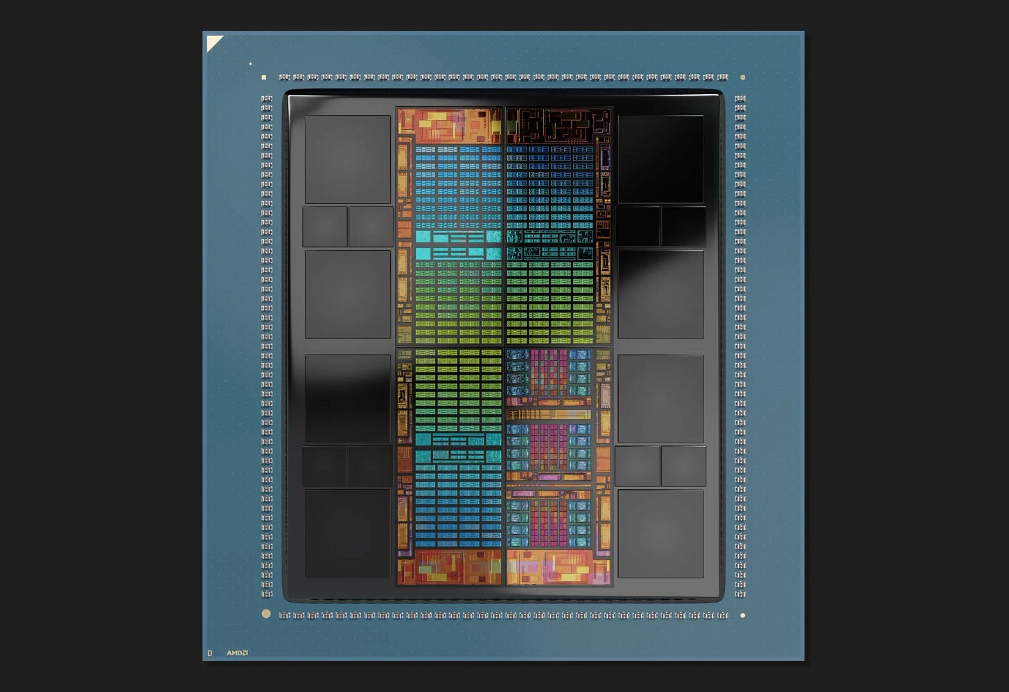
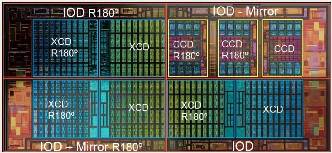
However, cross-socket or multi-node communication still relies onInfinity Fabricor Ethernet, which are electrically limited. Packaging and power constraints also cap the number of dies that can be integrated. By comparison, Passage’s3D photonic stackingoffers a more aggressive scaling path—not limited to heterogeneous elements within a single module, but enabling arbitrary numbers of chiplets to interconnect via a photonic baseboard, effectively forming a “giant APU.” While AMD has not explicitly committed to photonics, scaling Infinity to tens of tightly connected GPUs in the future will likely require optical technology.
System Interconnect Trends:
Beyond chipmakers, system vendors and cloud providers are also advancing interconnect technologies. Hyperscale datacenters are exploringoptical backplanesandphotonic switches. Meta has proposed building an “AI super-network” with optical fabrics, while Intel and Cisco are actively developingCPO-based switchesthat place optical transceivers directly beside switch ASICs to reduce insertion loss and improve port density.
These efforts can be seen as Scale-Up at thesystem level—treating the entire network as a single computer, with optical links tightly connecting nodes. Lightmatter Passage can be viewed as an extension of this concept at the machine level: providing a modular photonic interconnect platform that brings compute units logically to near-zero distance. As the industry pursues a fusion of Scale-Out and Scale-Up,photonic interconnects are becoming a central focus, spanning from processor internals to packaging, rack-level systems, and datacenter networks. Copper links are gradually being replaced by optical fibers.
Taken together, a comparison of Passage with other approaches shows that today’s AI acceleration race is not only about raw compute performance but also aboutinnovation in interconnect and packaging architectures. Through photonic 3D stacking, Lightmatter offers a viable path to break past the bottlenecks of traditional Scale-Out, potentially setting the stage for broader industry adoption of photonic interconnect technologies.
Analysis and Summary
Scale-Out vs. Scale-Up should not be viewed as opposites but rather as ends of a spectrum. Traditionally, Scale-Out provides flexibility and incremental growth, but as systems expand, marginal returns decline (due to Amdahl’s Law and rising communication costs). Scale-Up offers higher per-resource efficiency but is constrained by hardware limits and cost, preventing unbounded growth.
Future AI infrastructure will likely balance the two—what might be called “moderate Scale-Up + coordinated Scale-Out.” For example, dozens or hundreds of compute chips may be packaged into photonic interconnect modules, which are then linked together via high-level networks. This is precisely the vision behindLightmatter Passage.
Experiments such as theNaturephotonic processor andCerebras WSErepresent extreme Scale-Up, proving what’s possible within a single node. Meanwhile, NVIDIA and AMD are incrementally injecting Scale-Up elements into Scale-Out frameworks (chiplets, faster inter-node links).
In the coming years,photonic interconnects will play a critical enabling role, transforming large-scale compute architectures from loosely distributed clusters into tightly bound optical fabrics. For end users, this means larger models, faster training, and lower energy-per-compute.
In short, the Scale-Out/Scale-Up boundary is being redefined byoptoelectronic integration, and Lightmatter Passage provides a compelling example of how both benefits can be combined to meet the massive compute demands of next-generation AI.
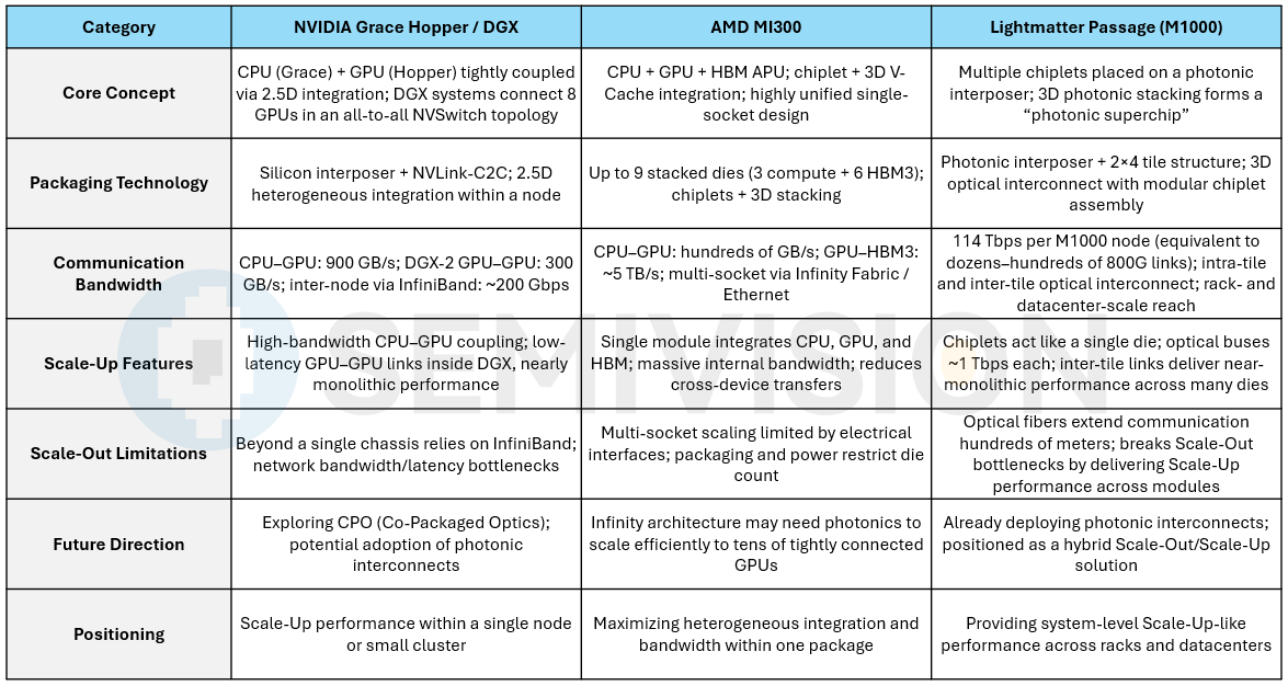
Scale-Out vs. Scale-Up should not be seen as opposites, but rather as two ends of a spectrum.
Traditionally, Scale-Out offers flexibility and incremental growth, but once systems reach a certain scale, diminishing returns become apparent (constrained by Amdahl’s Law and communication overhead). Scale-Up, on the other hand, delivers higher efficiency per unit of resource, but is limited by hardware boundaries and cost, making unbounded scaling impractical.
The future of AI infrastructure will likely seek a balance between the two—what could be called“moderate Scale-Up + coordinated Scale-Out.”For example, dozens or even hundreds of compute chips may be packaged into photonic interconnect modules, which are then linked through advanced networks. This is precisely the direction pursued by technologies likeLightmatter Passage.
TheNaturephotonic processor andCerebras WSErepresent extreme Scale-Up approaches, demonstrating the feasibility of breaking traditional limits within a single node. Meanwhile, companies such asNVIDIAandAMDare gradually introducing Scale-Up elements into a Scale-Out framework—via increased chiplet usage and faster node-to-node interconnects.
It is foreseeable that in the coming years,photonic interconnects will play a key enabling role, shifting large-scale compute architectures from loosely distributed systems toward tightly bound optical fabrics. For end users, this meanslarger models, faster training, and lower energy cost per computationwill become achievable.
In summary, the boundary between Scale-Out and Scale-Up is being redefined throughoptoelectronic integration, andLightmatter Passageprovides a compelling example of how the strengths of both approaches can be combined to support the massive compute demands of next-generation AI.
Distance Limitations of Copper Interconnects and Power Density Challenges
Technical Background and Challenges
Traditional electronic interconnects rely on copper wiring to transmit electrical signals. However, copper-based media are increasingly running into physical limits at high frequencies and data rates.
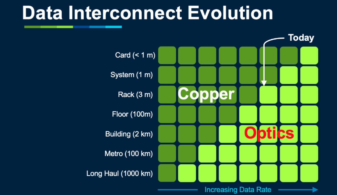
First,the transmission distance of copper is limited. As frequency increases, conductor and dielectric losses rise sharply, and high-speed signals may suffer severe distortion after only a few centimeters—requiring repeaters or pre-amplifiers to compensate, which adds extra power consumption and latency. In datacenters, copper cables are rarely used beyond tens of meters, with optical fibers already the norm for server-to-server connections. A similar problem occurs at the package and PCB scale: today’s high-speed SerDes (e.g., 112 Gbps PAM4) used for GPU-to-GPU communication suffer from channel loss and crosstalk when routed through PCB connectors, necessitating DSP-based equalization consuming several watts just to maintain signal integrity.

Second,the power consumption of copper interconnects increases linearly—or faster—with distance. Signal amplitudes must be boosted for longer traces, raising transmitter power, while receivers require high-speed clock recovery, amplification, and equalization, all consuming significant energy. Modern high-speed SerDes typically consume several picojoules per bit transmitted. Aggregated across wide links, this becomes a major power burden. For example, NVIDIA’s H100 GPU has ~900 GB/s of NVLink bandwidth; assuming ~10 pJ/bit, the I/O energy can reach tens of watts. Scaling to communication demands in the hundreds of Tbps, pure electrical solutions become impractical, as I/O alone could consume hundreds of watts.
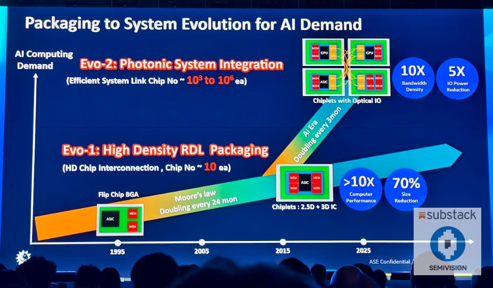
Third,I/O pad count and wiring density are fundamental bottlenecks. As the number of on-die compute units increases, the demand for I/O pins rises proportionally. Yet bump pitch on advanced packages is limited—currently around ~100 µm—and each transceiver circuit occupies ~0.015 mm². Even disregarding signal interference, fitting tens of thousands of I/Os around the periphery of an 800 mm² die is extremely difficult and costly. Silicon interposers and advanced packaging (e.g., EMIB, SoIC) can slightly improve I/O density, but they remain constrained by 2D layouts. Meanwhile, compute performance is scaling faster than I/O growth, leading to the common bottleneck of “fast compute, but unable to move data out.”

Beyond distance and bandwidth,power density is another major challenge. With Moore’s Law slowing, performance gains increasingly come from packing more circuits (e.g., more cores) into the same die or package. But power delivery and cooling capacity have not scaled proportionally. As a result, the power density (W/mm²) continues to climb, creating greater demands on packaging materials and thermal management.
If power density is too high, heat cannot be removed quickly enough, causing chips to throttle or even fail. Today’s advanced GPUs already reach ~0.5–0.7 W/mm², requiring large heatsinks and liquid cooling. In large 3D integrations, multiple high-power chiplets concentrate heat, compounding the thermal flux density. For example, assembling four 170W chiplets yields a 680W module, with extreme cooling challenges. Delivering such high currents into a 3D-stacked package also requires specialized technologies, such as dense TSV power vias and multilayer power distribution networks.
In short, in the era of copper interconnects,long-distance high-speed transmissionandhigh power density for supply and coolingare interlinked challenges: the former limits system scale, while the latter constrains performance integration within a unit.
Passage Technical Details
TheLightmatter Passageplatform directly addresses the bottlenecks described above.
Distance and Bandwidth:
Passage replaces copper wires withoptical waveguides and fibersas the transmission medium. Optical signals experience extremely low loss in silicon waveguides, enabling chip-to-chip or even rack-scale transmission over tens of centimeters to several meters without repeaters—an enormous advantage compared with copper, which exhibits severe attenuation within just a few centimeters.

In addition, optics enablewavelength-division multiplexing (WDM)to boost per-channel bandwidth density: each Passage optical waveguide carries 8 wavelengths at 56 Gbps each, achieving448 Gbps per waveguide. Sixteen such waveguides form a singleoptical buswith a throughput of~7.17 Tbps, far exceeding the density achievable with dozens of parallel differential copper pairs.
This “parallel by color” approach multiplies the information capacity of a single fiber. For instance, a Passage fiber transmits 16 bidirectional wavelengths simultaneously, delivering~1 Tbps full-duplexthroughput with only~100 mW per fiber. By contrast, achieving 1 Tbps bidirectional over copper would require tens to hundreds of high-speed lanes, with much larger volume and far higher power consumption.
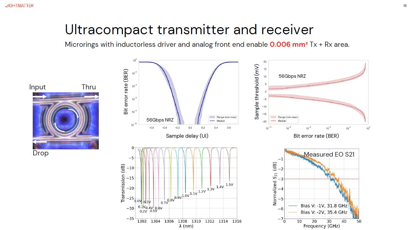
Passage also leveragesmicroring resonator modulators, shrinking optical transceivers to unprecedented size and power levels: each Tx/Rx pair occupies just0.006 mm², compared to ~0.015 mm² for typical electrical SerDes—a ~3× reduction. This density enables integration of thousands of optical I/Os in 3D stacks. Moreover, microrings have ultra-low drive power (~1 mW per device), yielding modulation energy of~0.018 pJ/bit. After accounting for laser and driver overhead, total energy per bit is expected to approach1 pJ, several times more efficient than state-of-the-art copper SerDes.
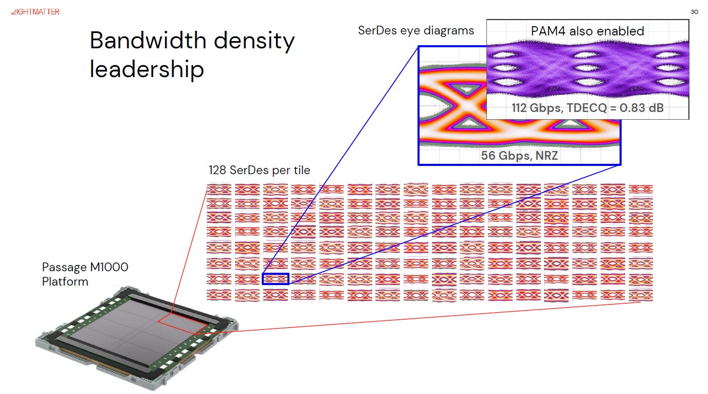
Internal Lightmatter tests show that optical links operate stably at56 Gbps NRZand112 Gbps PAM4, with BER meeting communication requirements. At 112 Gbps PAM4, the eye diagram remains open, and TDECQ extinction ratio is just0.83 dB. This demonstrates that optical interconnects not only match but may surpass the single-channel bandwidth of the latest copper SerDes—while consuming virtually no additional power over longer distances.
Power Density and Delivery:
While Passage’s 3D stacking concentrates multiple high-power dies, it incorporates robust power and thermal management measures. The photonic interposer integrates denseTSV power viascapable of carrying>2.5 A/mm²vertically, ensuring stable distribution of hundreds of watts within a 3D package.
Lightmatter demonstrated this with a369 mm² silicon thermal test chip, simulating distributed loads of1.47 W/mm²(equivalent to ~170W per die). Results confirmed stable power delivery through the TSVs and interposer. Based on this, the Passage M1000 is expected to support multiple150–200W-class compute diessimultaneously without supply bottlenecks.

Thermally, 3D stacking shortens heat paths: high-power compute dies can be cooled directly from the top surface, while the photonic interposer can integrate thermal conduction layers or even liquid cooling underneath if necessary. Compared with distributed multi-node cooling (where each node requires independent solutions), Passage’s centralized thermal design can be more easily optimized—for example, using a single cold plate spanning all chiplets to improve efficiency.
By replacing copper with optics, Passage dramatically extends interconnect distance and bandwidth, while its 3D electro-thermal design mitigates the challenges of high power density. It demonstrates that with the right approach, even nodes aggregatingthousands of TB/s of bandwidth and approaching kilowatt-level powercan operate reliably within physical limits. This provides a clear path forward for breaking through the constraints of traditional copper interconnects.
Comparison with the Photonic AI Processor inNature
TheNaturephotonic processor also touches on the limitations of copper interconnects, but its emphasis lies incomputational accuracyand the balance of hybrid optoelectronic systems. The processor demonstrated near-electronic accuracy across multiple experiments, showing that with careful calibration and architectural design, noise and stability issues in optical computing can be managed.
Although theNaturework does not directly address long-distance communication, its packaging strategy inherently controls distance: photonic cores and electronic controllers are co-packaged on an organic substrate, separated by only a few millimeters. This ensures that electrical signals (e.g., analog signals from the PTC to the DCI) do not degrade excessively. For external connectivity, the paper mentions the use ofMT optical connectors, likely for importing laser sources or exporting results—an indication that even this design partially relies on optics for external data transfer, especially when handling large volumes of information.
By comparison,Lightmatter Passagetakes a more aggressive approach, extending photonics toall inter-chip communication, whereas theNatureprocessor uses optics only for internal computation and limited I/O, with inter-die communication still handled by short-range electrical circuits.
Comparison with Other Industry Approaches
The limits of copper interconnects are evident across the industry and have prompted different responses:
Advanced Packaging and Buses:
NVIDIA and AMD optimize at the packaging level. For example,HBM memory stacksare connected directly to GPUs through silicon interposers, reducing path length from PCB traces to just millimeters and enabling>1 TB/s per GPUmemory bandwidth. IBM and Intel have also explored silicon photonic IP; Intel even proposed replacing CPU socket buses (QPI/UPI) with optical links, though early implementations were held back by transceiver size and cost.
In switches,Co-Packaged Optics (CPO)has emerged as a hot area: Cisco and Microsoft have tested systems embedding dozens of optical transceivers around switch ASICs, enabling direct optical I/O without retimers. These efforts align with Lightmatter Passage’s goals of removing “the last few inches” of copper. The difference: Passage pushes the concept further—from board-level CPO to chip-to-chip optical interconnects. NVIDIA, for instance, plans to adopt CPO in future “Kyber” racks to support600 kW-scale GPU systems, whereas Lightmatter already demonstrateshundreds of Tbps connectivity within a single supermodule, reducing reliance on rack-level switching and potentially reshaping system topologies.
Energy Efficiency:
To reduce copper interconnect power, companies have invested heavily in SerDes innovations, such asPAM4 signalingand DSP/FEC equalization. Yet these methods often tradepower for bandwidth: each new generation raises energy per bit. For example, moving from 56G PAM4 to 112G PAM4 significantly increased energy costs and thermal burdens.
Graphcore has pursued a different strategy, lowering per-lane speed but integrating more chiplets within a package to spread power. While effective at the card level, this still depends on conventional interconnects for scaling across cards. Moreover, as process scaling has slowed, I/O driver swing voltages are no longer shrinking fast enough, meaning energy per bit cannot decline like logic compute efficiency under Moore’s Law. Even NVIDIA and AMD have acknowledged in papers that future electrical I/O could consume the majority of system power.
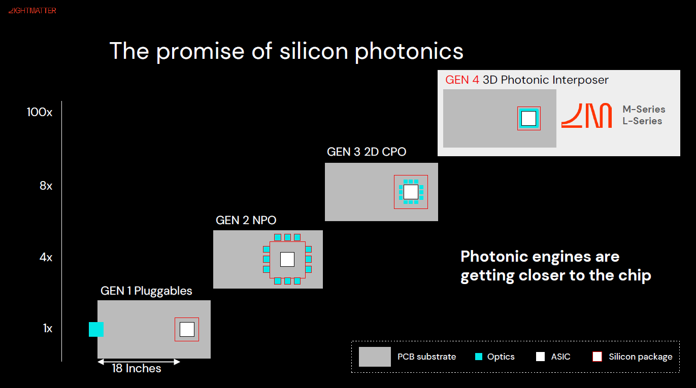
This makes photonic interconnects an inevitable path: optics do not suffer from RC constraints, can transmit long distances with very low signal power, and microring modulators provide exceptional energy efficiency. Lightmatter reports that its3D photonic CPOcan achieve8× chassis bandwidth improvement at half the powercompared with traditional 2D CPO—an order of magnitude leap not possible by incremental SerDes tweaks.
In the electrical world,distance and bandwidth are trade-offs: signals can go far or fast, but not both.Power densityacts as a double-edged sword—concentrating energy but also heat and reliability risks. Photonics introduces new dimensions to address both:
Using light for signalingenables “fast and far”: ultra-low loss, unaffected by capacitance, and multiplexed across multiple wavelengths within a single fiber.
Using 3D integration for specializationenables “distributed heat”: different layers handle compute, communication, modulation, and power delivery, while thermal loads are spread and managed more effectively.
3D interconnects also shorten power paths, reducing IR drop and stabilizing high-current delivery.
TheNaturephotonic processor validated the efficiency of hybrid optoelectronic systems at small scale, whilePassage M1000expands this to massive bandwidths and high-power integration, showing that even withthousands of Tbps bandwidth and near-kilowatt loads, photonic 3D integration can operate reliably.
We can expect growing adoption of photonic interconnects over the coming years—fromon-die, to inter-die, to full system-level fabrics. The copper bottlenecks that have long constrained engineers will gradually fade, freeing system architects. For the industry, this marks acomputing paradigm shift: compute scale will no longer be chained to communication limits, nor will rising power directly translate into crippling thermal density.
Lightmatter Passage represents the dawn of this shift—a vision of AI accelerators no longer bound by copper wiring, but built as three-dimensional assemblies where light weaves compute together at speed-of-light scales. We are standing at the threshold of thepost-copper interconnect era, and photonics is opening a new door to sustained compute scaling.
Passage 3D Photonic Stacking Solution Explained
Technical Background and Challenges
Building a system that breaks through traditional limits requires comprehensive innovation—from architecture to materials. Passage M1000, Lightmatter’s flagship technology, is centered on 3D photonic stacking, which integrates several critical elements: high-density optical transceiver arrays, optical waveguide interposers, heterogeneous chip bonding, and fiber-coupled packaging. Each of these comes with significant R&D challenges.
For example, integrating thousands of optical transceivers onto a limited silicon substrate demands drastic miniaturization of individual optical devices and reduction of crosstalk. Ensuring reliable optical transmission in a 3D package requires precise alignment of waveguides and fibers, optical via-fill materials, and consideration of temperature-induced variations in optical paths. Moreover, bridging optics and electronics poses a fabrication gap: high-speed CMOS circuits typically rely on advanced FinFET or GAAFET nodes, while silicon photonic devices are often fabricated with more mature processes (90nm or 130nm). Bringing the two together is a major hurdle.

At the system level, protocols and interfaces must be designed so that this novel optical interconnect can be used by general-purpose compute chips, not remain an isolated island. The emergence of UCIe (Universal Chiplet Interconnect Express) shows the industry’s desire for a unified chiplet communication standard—Passage must align with this. In short, the Passage 3D photonic stacking solution requires breakthroughs across device level (microring modulators), circuit level (inductor-less drivers, optical receiver front-ends), packaging level (photonic interposers, TSVs, fiber arrays), and system level (protocols, routing) before it can become a practical and complete solution.
Passage Technical Details

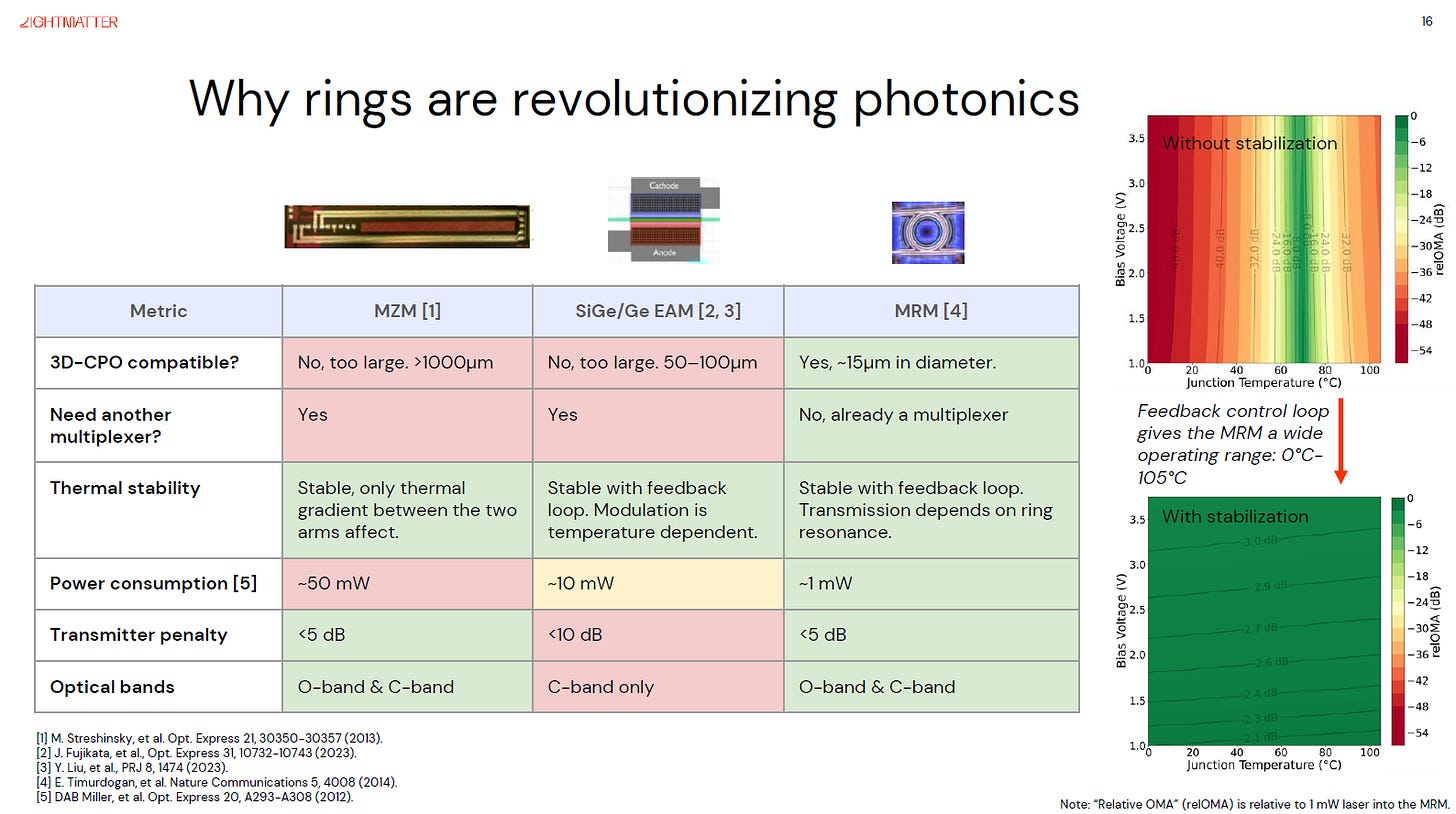
Themicroring resonator (MRR) modulatoris the heart of Passage’s photonic engine. A microring is a ~15 µm diameter circular waveguide coupled to a straight waveguide. Applying an electrical signal shifts the ring’s refractive index, altering its resonance with specific wavelengths and thus modulating optical intensity at high speed. Lightmatter chose microrings because they are compact, fast, and ideal for WDM (wavelength-division multiplexing).
By comparison:
Mach-Zehnder modulators (MZM) exceed 1000 µm in length, making large-scale integration impractical.
Electro-absorption modulators (EAM) are smaller but typically limited to a single C-band wavelength and require precise thermal stabilization.
Microrings, at ~15 µm diameter, can be densely arranged—hundreds within a few millimeters—and operate across O- and C-bands, allowing multi-wavelength coexistence. Their drawback is temperature sensitivity, but Lightmatter addresses this with integrated micro-heaters and bias control loops, keeping resonance stable from 0–105 °C. This makes system-scale deployment feasible.
Combined with inductor-less high-speed driver circuits and wideband analog front-ends, each optical transceiver unit occupies only 0.006 mm². The driver design eliminates bulky passive components, while the receiver front-end amplifies weak optical signals into digital form. These circuits are CMOS-compatible, enabling co-integration with microring arrays on the photonic interposer.
To further optimize power and area, Passage employson-chip multiplexing. Since microrings naturally act as wavelength-selective filters, chains of rings at different resonances form a built-in WDM mux/demux, eliminating the need for external optical multiplexers. In effect, microrings act as both “switches” and “wavelength combiners/splitters,” streamlining the 3D CPO (co-packaged optics) architecture.
Photonic Interposer
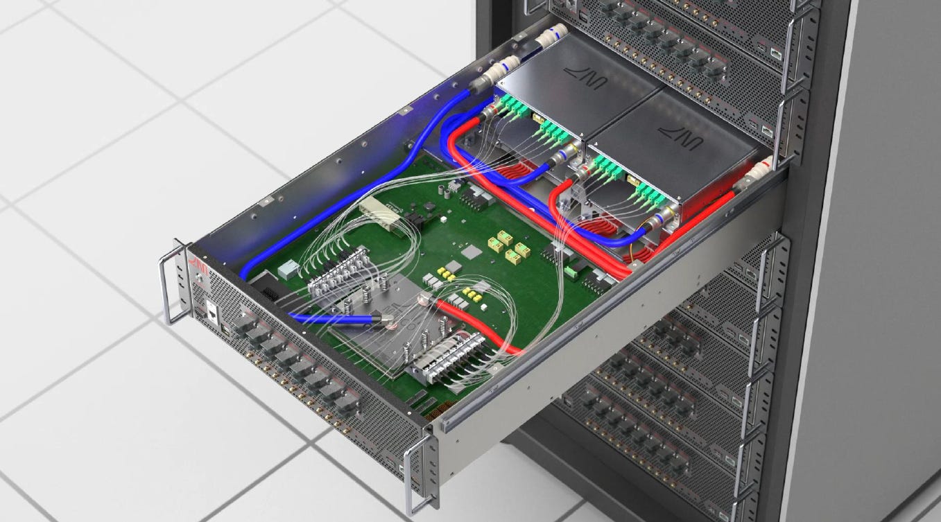
Thephotonic interposeris the hardware foundation of Passage. It is a custom silicon substrate containing dense optical waveguides and a reconfigurable optical switching fabric to carry chiplet-to-chiplet signals. Its top surface connects to compute chips (GPUs/TPUs, etc.) via micro-bumps or direct bonding, while the bottom is lined with fiber-coupled array interfaces for optical I/O.
The interposer is divided into 2×4 tiles, each containing 16 optical buses and switching matrices. Neighboring tiles are linked through vertical optical stitching to ensure seamless cross-tile communication. Tile boundaries also feature metallic bridges for direct low-latency electrical signaling between adjacent chiplets (e.g., emergency interrupts). Thishybrid optical-electrical designmaximizes flexibility: high-bandwidth bulk data is carried optically, while small synchronization signals are sent electrically.

Fabrication generally uses mature CMOS photonics processes (45nm or 90nm), balancing precise waveguide patterning with large substrate sizes. Extremely high flatness and alignment accuracy are required for bonding compute chips and fibers with minimal loss—Lightmatter likely employs advanced wafer-level bonding, achieving micron- or sub-micron alignment.
As a result, microring-modulated optical signals can couple into fibers or neighboring waveguides within just a few microns, minimizing insertion loss. Each Passage fiber interface supports up to 16 cores mapped to 16 waveguides. The full M1000 system includes 256 fibers, bundled into cables that connect to optical backplanes at the rack level, forming large-scale photonic communication links.
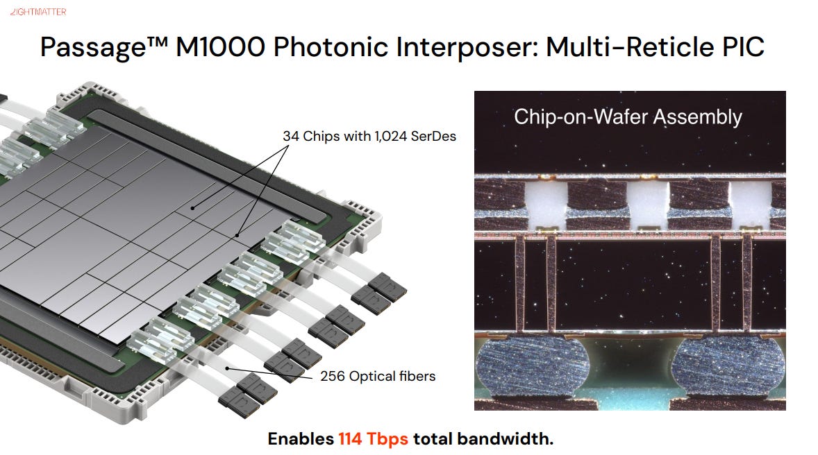
In summary, the photonic interposer is thephysical backbone of Passage—integrating optics, electronics, and packaging into one platform, and embodying the essence of 3D photonic stacking.
UCIe and Interface Protocols
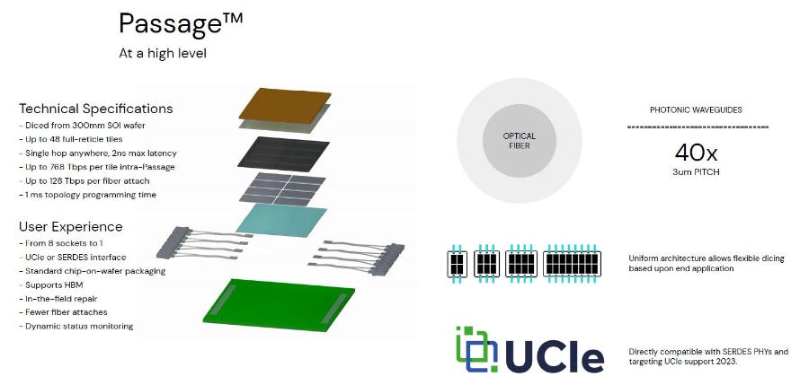
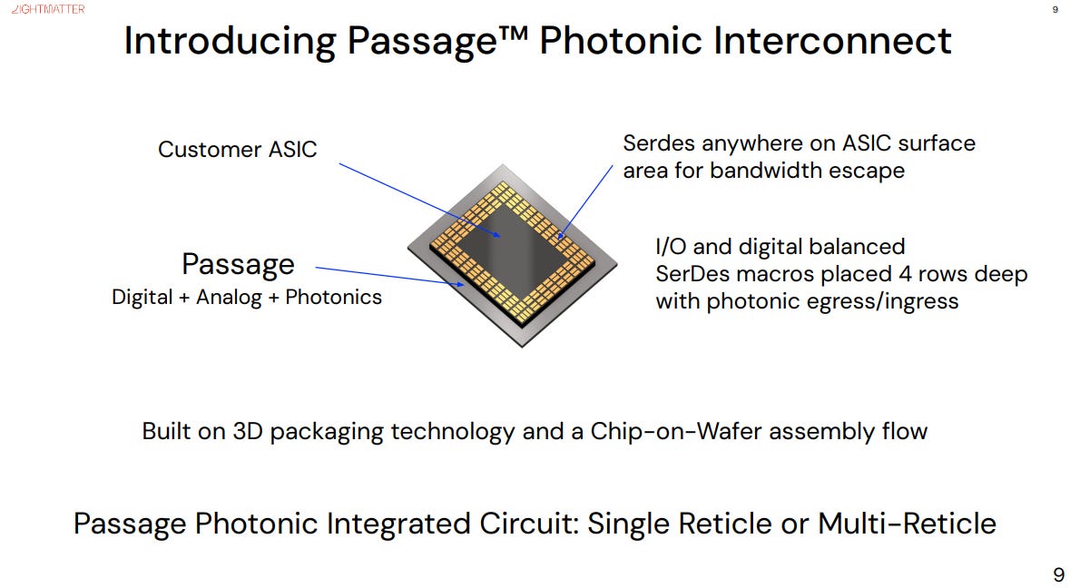
To ensure that various compute chiplets can easily leverage Passage interconnects, Lightmatter emphasizes compatibility with standard interfaces in its design. According to the presentation, a customer’s ASIC only needs to integrate a UCIe IP block to connect to the Passage platform.
UCIe (Universal Chiplet Interconnect Express) is an open, unified chip-to-chip interconnect standard, offering PCIe-like data exchange protocols but operating over high-speed links inside a chip package. Passage directly converts the high-speed SerDes signals defined by UCIe into optical signals, transmits them through the photonic network, and reconverts them back into UCIe electrical signals at the destination chip.
From the chiplet’s perspective, it simply connects to a “virtual bus” via UCIe, while the actual bus is carried by Passage’s optical fabric. This design dramatically lowers the adoption barrier—chip vendors don’t need to understand photonics at all. As long as they support UCIe, they can transparently enjoy bandwidth at the hundred-Tbps scale.
Passage also provides a complete reference system, including the photonic interposer (Passage PIC), external multi-wavelength light source modules, and standardized fiber couplers. This means Lightmatter is not selling standalone chips but aplatform solution, making it easier for customers to integrate photonics into their AI systems. For example, a GPU vendor could package its GPU die together with the Passage interposer and immediately gain optical interconnect capabilities, without developing photonic devices in-house.
Lightmatter also mentioned a strategic collaboration to co-develop anEIC (Electronic Interconnect Chip)—likely a companion chip that integrates opto-electronic protocol conversion, buffering, and switching logic, managing optical link scheduling and error recovery. The EIC could either be embedded within each chiplet or exist as a standalone management chip overseeing the entire optical network.
Overall, the technical details of Passage 3D photonic stacking showcase Lightmatter’s comprehensive engineering integration: from choosing microrings as core devices, to building the photonic interposer hardware, to adapting standard protocols and delivering a full platform solution. They have effectively woven photonics into the backbone of mainstream compute platforms, providing an almost plug-and-play optical interconnect infrastructure. This layered and tightly integrated approach is precisely what enables 3D photonic stacking to move from concept to practical deployment.
Comparison: Photonic AI Processor inNature
TheNaturephotonic processor also adopts a multi-chip vertical integration scheme, but its focus is onphotonic computation itself rather than interconnect generality. In this design, thephotonic tensor core (PTC)performs analog computation by using light intensity to represent matrix operations. Each PTC contains128 10-bit photonic vector unitsand128×128 7-bit photonic weight units. This architecture requires a specialized instruction set and calibration procedures, coordinated by64 RISC-V coresin the digital control interface (DCI).
The difference between theNaturephotonic processor and Passage is similar to that between aSoCand anetwork switch: the former is tightly coupled and optimized for a specific workload, while the latter provides flexible interconnection across diverse units. In the future, if theNatureprocessor evolves further, it may need to integrate Passage-like optical interconnects to link multiple photonic compute modules together, overcoming the single-card limitation.
Packaging Technologies
TheNaturephotonic processor uses anorganic substratefor heterogeneous integration, while Passage uses asilicon interposer. Organic substrates offer large size and lower cost, but lack the fine interconnect density of silicon interposers. Silicon interposers providemicron-scale routing pitchand support embedding passive devices, making them more suitable for high-frequency signals.
In theNaturedesign, photonic cores and control chips are connected through short organic substrate traces, with limited bandwidth but sufficient for matrix compute pipelines (the paper reports1024 GB/sbetween PTC and DCI). Passage, by contrast, requires massive parallel channels, achieved with silicon interposer waveguides and TSVs. It is not hard to imagine that ifNaturesystems scale up, they too may adopt silicon interposers for higher chip density and connectivity.
Complementary Roles
In summary, theNaturephotonic processor achieves breakthroughs in“how to compute with light,”while Passage solves“how to connect with light.”Their approaches are different but complementary. If in the future high-performance photonic compute cores are interconnected via Passage’s optical fabric, it may be possible to build a large-scale AI acceleration platform entirely mediated by light—combining the strengths of both.
Comparisons with Other Industry Players (NVIDIA, Cerebras, etc.)
Ayar Labs and Optical I/O:
Ayar Labs focuses on silicon-photonics-based optical I/O chips, designed as companion dies to standard processors. TheirTeraPHY photonic chipletattaches via 2.5D integration, offering hundreds of Gbps per pin. This approach is similar in spirit to Passage—bringing photonics close to or into compute chips. However, Ayar’s products currently targetboard-level connections(e.g., CPU to remote accelerator cards), with bandwidths in theTB/s rangeand limited topoint-to-point links. Passage instead advances toin-package, multi-point switching, going further. Ayar has also collaborated with Intel under DARPA programs to place optical I/O directly inside CPU packages, pushing toward a “photonic system bus.” This indicates growing industry acceptance of optical interconnects, though Lightmatter stands out with combined experience inboth photonic computing and interconnects.
TSMC SoIC / Intel Foveros (3D technologies):
Foundry/IDM giants TSMC and Intel provide various 3D packaging platforms (chip stacking, wafer-to-wafer bonding, etc.). For example, Graphcore’s Bow IPU uses TSMC’sSoIC WoW. These technologies currently integrateelectrical chips(logic, memory, PMICs), still relying on copper. If Passage succeeds, it could spur foundries to incorporateoptical channelsin 3D packaging—e.g., leaving optical through-vias in standard platforms to facilitate stacking of photonic and logic layers. This would accelerate optical interconnect adoption. Key challenges will include material/process compatibility (e.g., SiN waveguides, high-Q microrings with advanced CMOS). Lightmatter’s pragmatic path—fabricating the photonic interposer on mature nodes and bonding it with 7nm/5nm logic dies—shows a feasible compromise.
IBM “Zero-Change” Photonics:
IBM Research proposed integrating silicon photonics into CMOS without altering the standard process—reusing existing metal layers as waveguides and antennas. While performance is limited, this demonstrates integration potential. If matured, every GPU could natively include optical I/O, reducing the need for external photonic interposers. This would pressure proprietary solutions like Passage. However, given the material and structural demands of high-performance photonics (e.g., absorption thresholds, waveguide roughness), such zero-change methods are unlikely to match specialized photonic processes soon. Thus, Passage’s heterogeneous integration approach remains the practical near-term solution.
NVIDIA / Cerebras:
NVIDIA has not yet deployed photonic interconnects in products, but its R&D focus suggests interest. Cerebras, though not optical, achieves214 Pb/sbandwidth in its WSE through a dense 2D electrical mesh. However, this is confined within a single wafer-scale chip. Scaling such interconnects off-chip would require optics—making Passage a natural extension, essentially exporting “214 Pb/s fabrics” to the system level.
Graphcore’s IPU-Fabric delivers>2 Tbps per IPUfor rack-scale clusters. This is similar to Passage’s scale (each Passage tile: 128 channels × 112 Gbps =14.3 Tbps; 8 tiles =~100 Tbps). However, Graphcore relies on copper cabling, with distance limits and lower efficiency, while Passage leverages optics for scalability and efficiency.
Analysis and Conclusion
Compared to theNaturephotonic processor, which focuses on algorithmic and computational breakthroughs, Passage is asystems-engineering achievement: assembling mature components into a novel combination, and offering an end-to-end solution ready for industry adoption. This“build the bridge first, pave the road later”approach may accelerate the commercialization of photonics in AI accelerators.
Looking across competitors, some focus onphotonic computation, others ondense packaging. Lightmatter uniquely translates photonic computing know-how into apractical photonic interconnect product, opening a new front. The industry is likely to advance along two converging lines—“computing photonicization”and“interconnect photonicization.”Passage, as today’s leader in photonic interconnects, provides ablueprint and proof point: demonstrating that 3D photonic interconnects are not only feasible under commercial conditions, but offer immense advantages.
In short, Passage 3D photonic stacking is more than a technical breakthrough—it is anew system-building philosophy: using light to construct the highways between compute units, enabling hardware architects to reimagine the landscape of multi-chip AI systems.
Breakthroughs in Bandwidth Density and Energy Efficiency
Technical Background and Challenges
Bandwidth densityrefers to the data rate deliverable per unit connection area or per single interconnect medium, whileenergy efficiencyis typically measured in energy per transmitted bit (pJ/bit). These two metrics set the upper bound on how much communication an AI supercomputing system can support within limited space and power budgets.
In traditional electronic solutions, bandwidth density is constrained by package pin count and trace pitch. For example, a PCIe Gen5 x16 interface offers only about 128 GB/s of total bandwidth because connector size and pin count limit the number of differential pairs. Similarly, even advanced HDI PCBs cannot route high-speed traces arbitrarily densely without incurring crosstalk and signal-integrity issues.
By contrast, optical fiber carries far more information. A single ~0.5 mm-diameter fiber can carry several Tbps—or more—via WDM and higher-order modulation, whereas a metal bundle of similar thickness cannot reach that scale. Meanwhile, the energy efficiency of electronic links worsens as speed rises: moving from NRZ to PAM4 doubles bandwidth but demands higher SNR, increasing TX power. Optical modulation is comparatively linear: whether one wavelength at 56 Gbps or sixteen wavelengths each at 56 Gbps, themarginalpower increase is modest so long as laser power suffices. As a result,per-bit energyin optics is lower at high aggregate bandwidths. Concretely, state-of-the-art SerDes consumes ~10–15 pJ/bit at 112 Gbps PAM4 (including TX/RX DSP), whereas experimental silicon-photonics links report as low as ~2–5 pJ/bit (excluding lasers), with the advantage growing over distance.
For AI training systems, higher bandwidth density means sufficient data exchange within a limited package footprint to coordinate hundreds or thousands of TOPS; higher energy efficiency means communication occupies a smaller share of total power so more can be devoted to computation. Today’s GPUs (e.g., NVIDIA H100) reach 3 TB/s HBM3 bandwidth by surrounding the GPU with many HBM stacks and very wide buses—an extreme use of package area. Looking ahead, model parameter-exchange rates may grow by multiples that electronics alone cannot match. Achieving a step-change in bandwidth density and energy efficiency likely requiresleaving copper’s scaling curve—the opening for photonics.
Passage Technical Details
What’s more, this114 Tbpsis not in a giant datacenter switch—it’s condensed into a package only a few centimeters across. A rough bandwidth-density estimate: assume an M1000 package of ~60 × 60 mm (inferred from 34 chiplets plus fiber interfaces), area ~3,600 mm², yielding ~31.7 Gbps/mm². By comparison, conventional PCB interconnects struggle to exceed~1 Gbps/mm². Through 3D stacking and multiplexing, Passage lifts density by one to two orders of magnitude.
Lightmatter sharedHot Interconnectsdata indicating that, versus a typical CPO (co-packaged optics) approach, Passage delivers6×the bandwidth for the same added package area, athalf the power. For example, if a conventional CPO requires a 50% package-size increase to reach a target bandwidth, Passage can achieve the same or higher bandwidth with roughly1/6that area increase—implying~8–12×higher bandwidth density than current CPO solutions. The presentation positions Passage as“Bandwidth density leadership”and shows clean eye diagrams at56G NRZand112G PAM4. With PAM4 qualified, per-channel rate doubles to112 Gbps; under8-λ WDM, each optical link can reach~896 Gbps, further raising the ceiling for system bandwidth density.
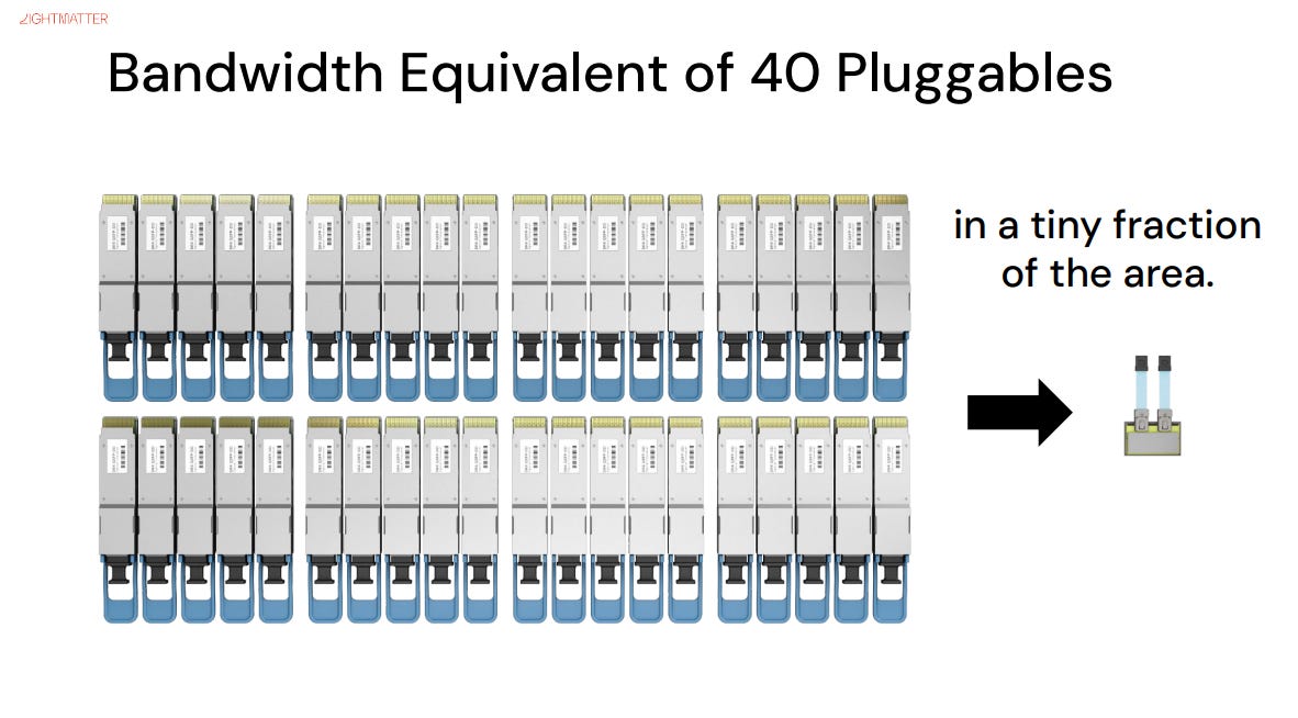
On energy efficiency, Passage leverages silicon-photonicsmicroring modulatorsto minimize energy per bit. Microring modulation is essentially a small-signal capacitive perturbation on a high-Q resonator, requiring very low drive voltages and currents (mA-class), hence low power. Lightmatter’s coherent-link measurements indicate that for the same distance, a Passage optical link delivers equal or greater bandwidth at~50%the energy of an electrical link. One model comparison shows that, in a given AI training chassis, adopting Passage cancut communication power by >50%whileboosting total bandwidth 8×—a major improvement to system-level performance-per-watt. Historically, large GPU clusters have wasted20–30%of power on communication stalls. By increasing bandwidth and lowering pJ/bit, Passagereturnsthat power to actual compute.
Crucially, Passage’s optical-link power isweakly dependent on distanceacross package-internal millimeters to inter-package meters, whereas copper often pays a multiplicative power penalty per added reach. Thus, Passage’s efficiency advantagewidensat larger scales. Lightmatter’s claim of>60% TCO reductionfor AI training accounts for these energy-cost savings: cheaper electricity and shorter training time flow directly into lower ownership cost.
Traditional Optics vs. Passage: Implementation Matters
Modular vs. Integrated:
Pluggable optics (QSFP+/OSFP) are discrete modules on switch cards—e.g., 16× QSFP56 yields ~25.6 Tbps per 1U board—with ~10 pJ/bit and long electrical runs from the ASIC. CPO brings optics near the ASIC to shorten traces and cut power, but remains2D area-limited. Passage putsoptical TX/RX arrays beneath the logic dies, vertically coupled in3D, effectivelystacking I/O layers(like adding high-rises to increase floor-area ratio). A single Passage module reaches~114 Tbps, rivaling rack-class switches. Integration yieldsMoore-likescaling; modularity yields only linear scaling.
Microrings vs. Other Modulators:
Conventional links often useMZMorEAM, which are larger and higher-power, limiting channel density (MZMs can be millimeters long). Microrings enablethousands of channelsper die—akin to the leap from vacuum tubes to transistors. Studies note that without microrings,Tbps-classon-die optical I/O is nearly infeasible. Choosing a “transistor-class” photonic device underpins Passage’s bandwidth-density breakthrough.
WDM vs. Parallel Fibers:
Traditional scaling adds more parallel fibers/cores. Passage packsmultiple wavelengths per fiber, multiplying capacity with only slight power rise thanks to spectral reuse. While16-λ DWDMis routine in telecom, shrinking it into thepackageis novel, requiring microring arrays precisely aligned to ITU channels with strong isolation—evidence that silicon-photonics waveguide fabrication is mature enough to support explosive density growth.
Dynamic Switching & Utilization:
High bandwidth is wasted if stranded on fixed links. Passage’soptical switchingdynamically re-routes capacity,poolingbandwidth where needed, raising utilization andeffectiveenergy efficiency—akin to virtualization at the fabric layer.
Analysis and Conclusion
Bandwidth density and energy efficiency are thecirculatory healthof an AI system. Lightmatter’s Passage uses photonics to elevate both to levels previously requiring an entire datacenter switch fabric—now within asingle package—while drivingper-bit energyto levels electronics cannot easily reach.
This is not just prettier numbers; itchanges system design. When bandwidth is no longer scarce, distributed architectures can be more flexible. When communication is nearly “free” and cool, software can aggressively move data among modules without energy penalties. We edge closer to“near-zero communication cost,”where compute units converse like densely connected neurons without overheating or congestion.
TheNaturephotonic processor also advancescompute energy efficiency, pushing overall AI efficiency higher. These trends, combined with industry demand forlow-carbon, high-compute, will drive hardware toward ever higherbandwidth/energyratios. Future supercomputers will be judged not only by PFLOPS, but also byeffective communication per wattandcompute utilization.
Looking back at these experiments, there are both inspiring signs and clear areas for further work:
What’s inspiring:Photonic AI hardware has moved from scientific concept to engineering reality. TheNaturephotonic processor used a series of ResNet/BERT results to show the world that optical computation is no longer limited to toy linear operations, but can handle complex deep-learning workloads with accuracy loss kept within a tolerable range. Lightmatter’s Passage, through communication tests and simulations, demonstrates substantial gains for real large-scale systems—especially for MoE, the architecture that stresses interconnects the most—where its3×+performance uplift signals enormous practical value.“We can finally keep computation from being dragged down by interconnects.”These experiments bear that out. The data greatly boosts confidence in photonic technologies and forces the semiconductor industry to recognize that photonics is not some far-off fancy, but the next step within reach.
What still needs work:How to scale up and comprehensively surpass electronics. Today’s photonic processors are still modest in compute, and Passage remains in the demo stage. We need to see photonic chips at 10× and 100× the current scale to truly rival—and exceed—the flagship products of NVIDIA/AMD. In theNatureexperiments, accuracy gaps remain on complex tasks like natural-language understanding; these will require hardware advances (e.g., higher-bit representations, better calibration) together with software support (e.g., optics-aware training). None of this is insurmountable: given time, photonics could see step-function gains akin to early GPUs versus CPUs.
From the overall performance results, the core value of photonics for AI hardware lies inexceptional energy efficiencyandcommunication capability—precisely today’s AI bottlenecks. Even if electronic hardware piles on more compute, it runs into power walls and interconnect walls that prevent full conversion into application performance; photonics offers a path around both. In experiments, the photonic processor neared FP32 accuracywithout special hyperparameter tuning, suggesting the software ecosystem can transition smoothly; Passage’s training-throughput gains show that, at the system level, optical interconnects can indeed weave compute units more tightly together. In other words, photonic hardware isunlocking more AI compute—reclaiming performance idling behind communication limits and frequencies throttled by power budgets.
In summary,success in the experimental-validation phase gives photonic AI computing a strong start. The next step is to validate on larger-scale training (e.g., GPT-class models) and face off directly against top-tier electronic systems. Based on current trends, that day isn’t far off. The performance results carry a key message: photonic computing isn’t meant to replace electronic computing, but toextend a Moore-like growth curve—to throw fresh fuel on the AI compute trajectory. The experimental data shows the spark is lit; over the next few years it may well blaze, pushing AI to unprecedented heights.
Lightmatter Passage M1000: A Photonic Interconnect “Superchip”
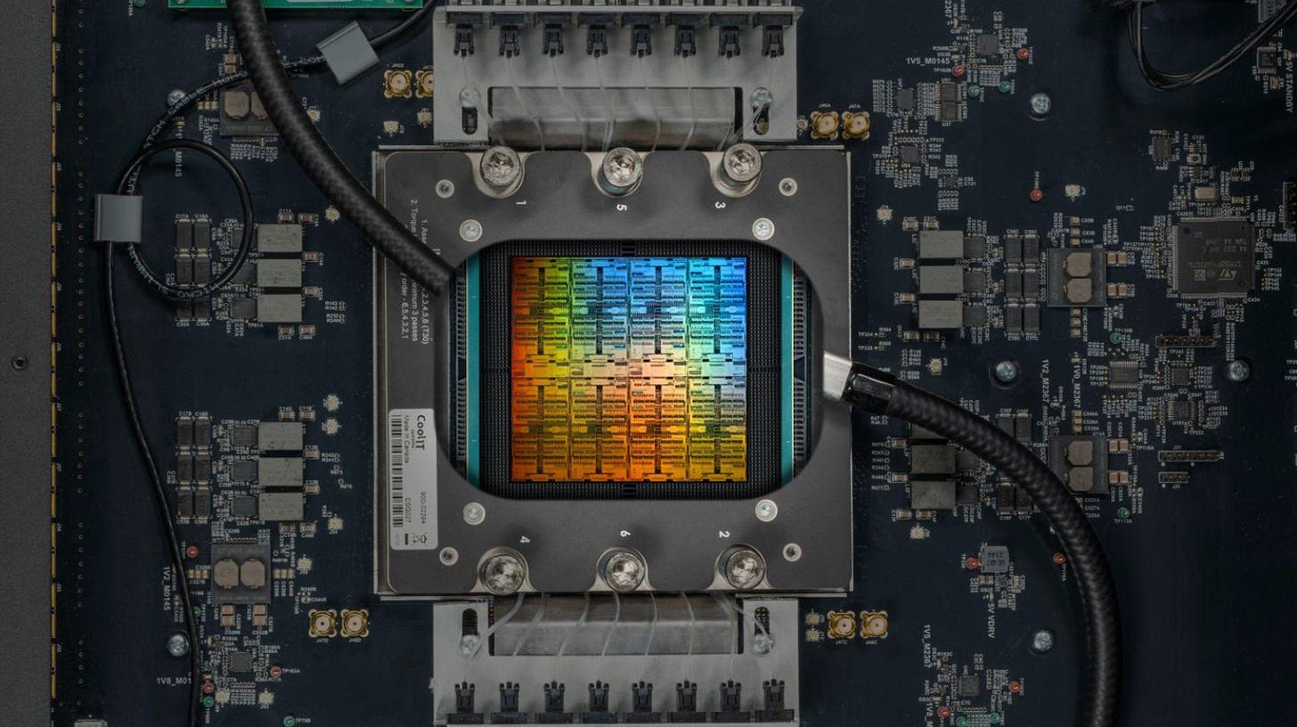
The Lightmatter Passage M1000, the industry’s first photonic-interconnect “superchip,” uses 3D packaging to merge dozens of compute chips into a single logical unit. It delivers over 100 Tbps of internal bandwidth, supports millisecond-scale dynamic optical path reconfiguration, and transmits data at just a few pJ/bit. This completely rewrites the traditional landscape of “fast compute but slow communication.”
Experiments and simulations show that in MoE training—an architecture most dependent on interconnects—Passage achieves 3–7× speed improvements, indicating it could dramatically shorten the training cycles of future ultra-large models. On the other hand, theNaturephotonic AI processor proved the feasibility of photonic compute cores: in tasks such as ResNet and BERT, it achieved accuracy close to 32-bit GPUs, with equal or better energy efficiency. This demonstrates that photonic computation is no longer “beautiful in theory” but already capable of handling mainstream AI workloads. With scaling and optimization, it has the potential to catch up to—and even surpass—traditional electronic accelerators.
Comparing NVIDIA, Cerebras, Graphcore, Tachyum
All of these players are addressing bottlenecks, but most remain stuck in the framework of “more transistors, faster SerDes.”
NVIDIA Blackwell/Rubinleverage 3nm nodes and HBM4 stacks to push compute into the PFLOPS range, but interconnect evolution (e.g., NVLink 6 at 3.6 Tbps) lags far behind compute growth.
Cerebrastrades a full wafer for enormous on-chip bandwidth, but expansion across wafers still requires traditional networking.
Graphcoreinnovates in per-card efficiency but struggles with multi-card scaling.
Tachyumaims for all-in-one chips but cannot escape multi-core interconnect limits.
By contrast, Lightmatter Passage takes a different route: breaking the interconnect bottleneck with photonics, while integrating seamlessly into existing ecosystems via UCIe. This approach can complement traditional compute roadmaps and elevate them further. Imagine:
NVIDIA adding a Passage optical backplane to Rubin, allowing hundreds of GPUs to behave like one system with massive performance gains.
Cerebras giving each WSE an optical interconnect interface to form a wafer-scale supercomputer with efficient networking.
Graphcore extending beyond its current 16/64-IPU Pods by using a fiber fabric.
In short, photonic interconnects and photonic compute will become the new normal in AI hardware—complementary to existing strengths and together building more powerful systems.
Future Outlook
- Photonic interconnects reach commercial scale first.
Because interconnects are today’s most pressing bottleneck, technologies like Lightmatter Passage will first be deployed in high-end AI training systems and datacenter switching networks. NVIDIA may release GPUs or switches with integrated optical modules (it has already previewed Spectrum-X, a photonic switch). Hyperscalers may adopt optical-interconnect racks with photonic backplanes to improve throughput and efficiency. Once top vendors validate photonic interconnects, industry adoption will accelerate. Component costs should fall with volume, while standards (e.g., OIF’s chiplet optical interconnect discussions) emerge. If Passage succeeds in deployment, it could become ade facto industry standard, catalyzing a broader “photonic packaging” ecosystem.
- Photonic compute begins catching up.
Although photonic compute chips remain limited today, theNatureprototype set a precedent. More startups and labs will likely develop second- and third-generation accelerators with better precision, scale, and generality: larger matrices (128 → 1024), higher bit widths (FP16/BF16 → FP32), and photonic memory elements (delay lines, storage rings) to reduce ADC/DAC overhead. Within 2–3 years we may see demo photonic accelerator cards running GPT-like models (initially small-scale, hundreds of millions of parameters), gradually scaling up. Longer term, as design and process mature, photonic accelerators could become major datacenter workhorses—especially inpower-sensitive inference scenarios. Imagine a photonic card delivering GPU-equivalent performance at tens of watts—hugely attractive for edge AI and large-scale deployments.
- Electron–photon hybrid architectures emerge.
Mainstream electronic giants won’t stand by. Future architectures may evolve toward heterogeneous integration:electronic logic + photonic interconnect + photonic compute. CPUs/GPUs might embed optical matrix-multiply units as co-processors (as Intel/IBM have explored). AMD could overlay optical channels onto Infinity Fabric. In the long run, SoCs may combine electronic control/memory units with photonic arithmetic cores. This hybrid approach will require new compiler and scheduling techniques but promises vastly higher compute density and lower power. AI leaders like OpenAI may also bet on photonics for differentiation.
- Software ecosystems adapt.
With photonic hardware, software frameworks must evolve. Future compilers and training systems will account for optical characteristics, enabling quantization-aware training and routing-aware parallelization to mitigate photonic imperfections and exploit their strengths. Examples: training strategies robust to optical noise, or topology-aware parallel algorithms that leverage optical interconnect flexibility. Hardware could also inspire model design: if interconnect bandwidth becomes abundant, models might rely more onglobal feature mixing—just as self-attention was enabled by GPU matrix-multiply capability. MoE already thrives on bandwidth; with even freer communication, model architectures could evolve toward more modular, cooperative designs.
- Industry collaboration and new landscape.
Photonics spans optics, semiconductors, and systems—requiring close collaboration across the supply chain. Foundries like TSMC may offer dedicated photonics process platforms, EDA vendors may deliver mixed electro-optical design tools, and OSATs may innovate in fiber-array bonding. This could give rise tonew supply chains and industry standards. Future AI accelerators may be hybrids: NVIDIA GPUs + Lightmatter interconnects + new “Lucent Memory” optical storage, for instance. The competitive landscape may shift: incumbents who miss the photonics transition could be leapfrogged by newcomers, while those who seize the moment may dominate AI hardware’s “second half.”
A deep dive into Lightmatter Passage confirms photonics’revolutionary potential in AI acceleration. Traditional bottlenecks are being pierced by light: compute scale is no longer bound by copper, and energy efficiency is no longer tied solely to Moore’s-law scaling. Over the next decade, AI may enter anew normal powered by electron–photon dual engines. Together, photonics and electronics will keep driving exponential compute growth to meet the needs of ever more advanced models.
From an industry perspective, this is a transformation on par with the rise of the GPU. Whoever masters and deploys photonic technology first may lead the next generation of AI infrastructure. As a pioneer, Lightmatter has already lit the spark; soon, that spark could ignite an industry-wide blaze. The future is bright—anAI era running at the speed of lightis fast approaching, poised to accelerate the intelligence revolution for all of society.

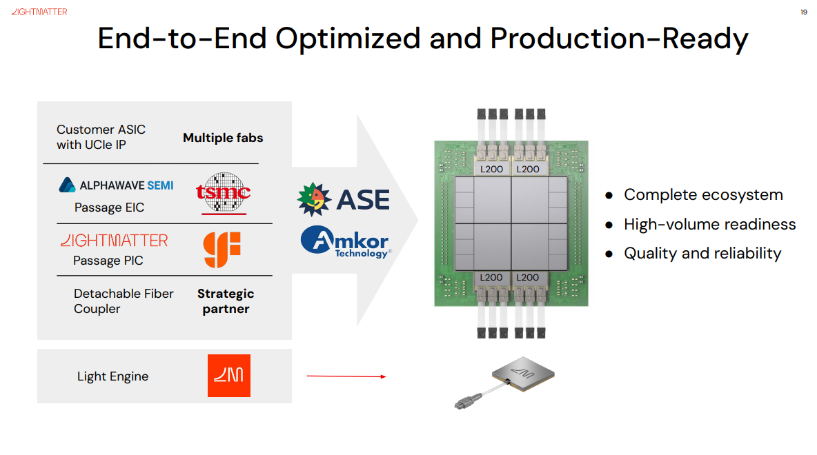


PreviousNext
TopLatestDiscussions









See all