Hot Chips 2025 | Meta Driving AR/VR Adoption: A Full-Stack Dissection of Smart Glasses from Sensing to Computing
Hot Chips 2025 | Meta Driving AR/VR Adoption: A Full-Stack Dissection of Smart Glasses from Sensing to Computing
- Source: SemiVision
- Author: SEMIVISION
- Published: 2025-09-04T22:04:47+08:00
- URL: https://tspasemiconductor.substack.com/p/hot-chips-2025-meta-driving-arvr Hot Chips 2025 | Meta Driving AR/VR Adoption: A Full-Stack Dissection of Smart Glasses from Sensing to Computing


Hot Chips 2025 | Meta Driving AR/VR Adoption: A Full-Stack Dissection of Smart Glasses from Sensing to Computing
Original Articles By SemiVision Research (Hotchip,TSMC,UMC,Samsung,Meta,Apple, NIL)

Sep 04, 2025
∙ Paid

AtTSMC’s 2025 Technology Forum, “robots” and “AR/VR smart glasses” were highlighted as the next wave of applications that will heavily depend on semiconductors. Among them, AR smart glasses present the most diverse challenges, as they simultaneously require high-performanceimage sensors (CIS), high-precisionoptical and motion sensors (MEMS), real-timevideo processing and recognition chips, and low-powerSoCstightly integrated with AI computing.
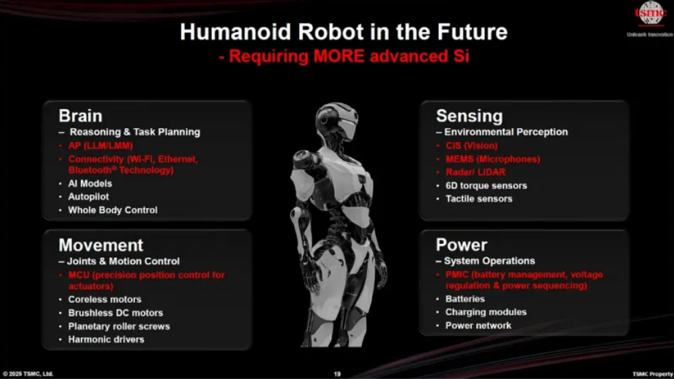
All of these components must be realized within an ultra-lightweight wearable form factor, which means the requirements forprocess technology, packaging, power management, and heterogeneous integrationare even more stringent than those for smartphones.
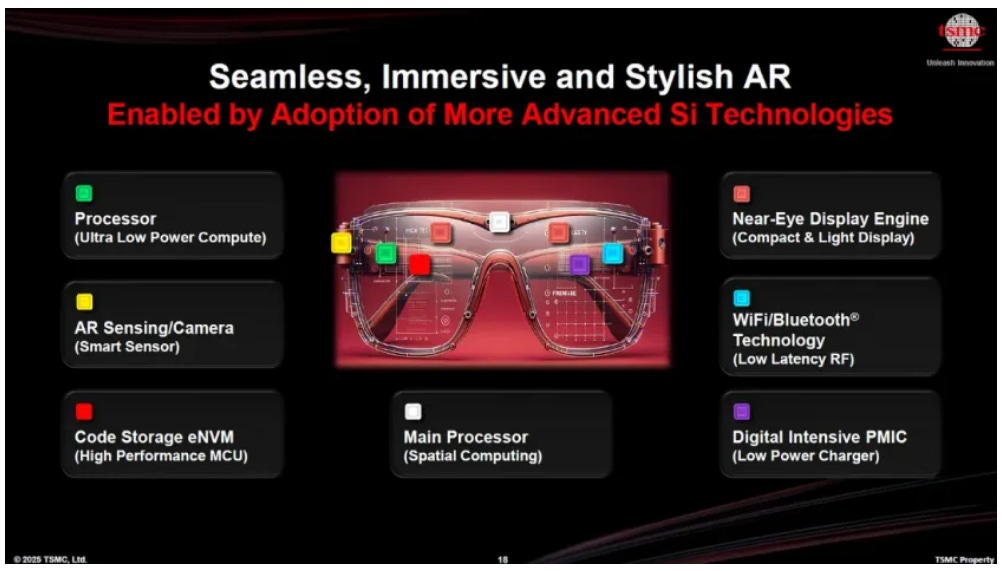
CIS is evolving from traditional FSI/BSI toward athree-layer stacked architectureto meet the demands of low-light imaging, HDR, and spatial sensing.MEMS sensors, covering IMUs (accelerometers and gyroscopes) as well as depth/optical MEMS, are critical for eye tracking and gesture control. Combined withacoustic and voice-processing chipsandAI vision recognition accelerators, they form a complete “sensing–processing–interaction” chain.
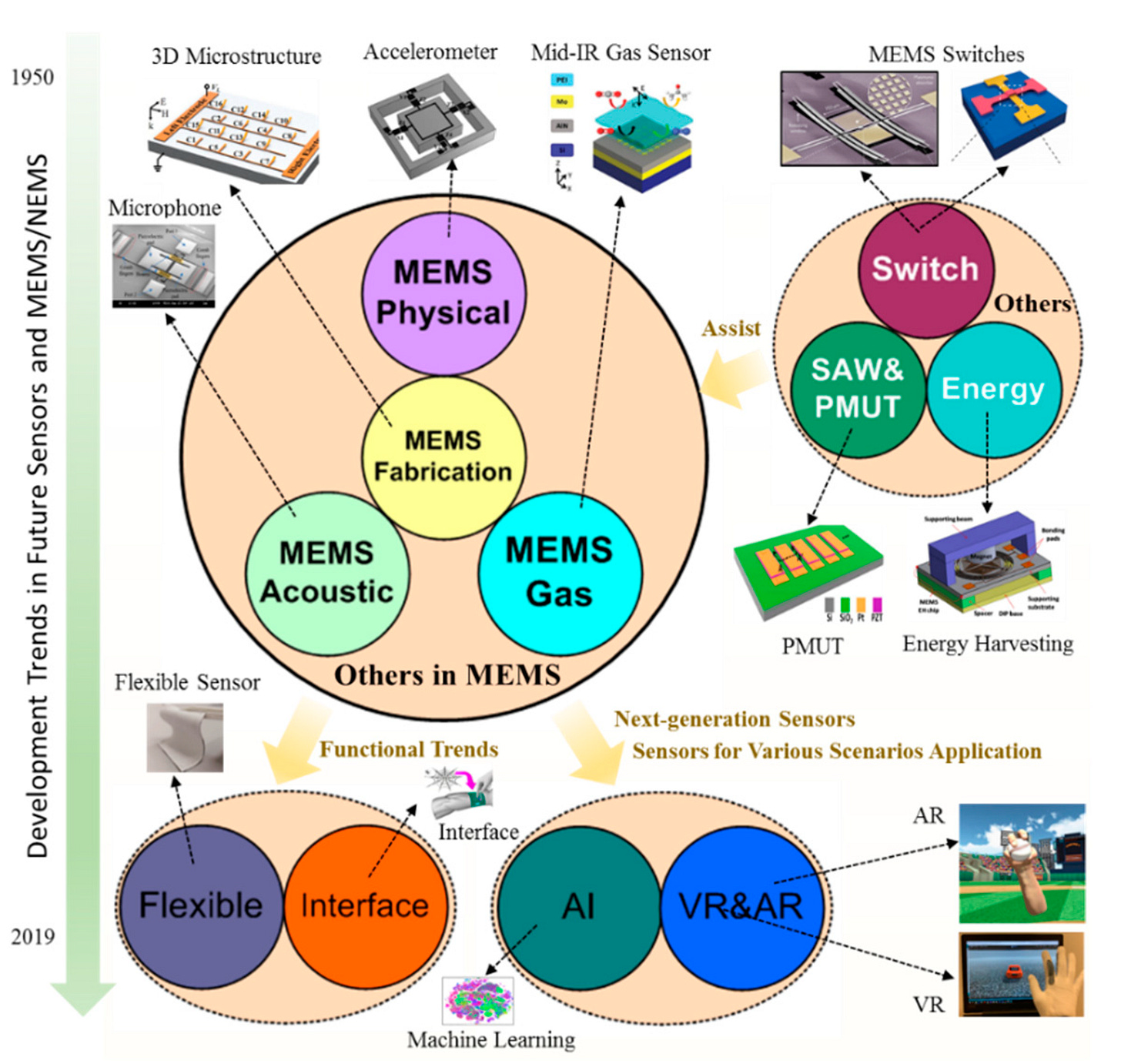
This trend is also driving foundries such asTSMC and UMCto actively invest in CIS, MEMS, and specialty platforms, while strengthening the role ofadvanced packaging and heterogeneous integration.
This article starts from the perspective ofcore chip requirements, analyzing in detail the progress ofCIS, MEMS, optical sensing, and AI-based audio-visual processingtechnologies in the implementation of AR smart glasses. It also updates the latest developments across the global industry chain, helping readers clearly understand how this cross-disciplinary application is driving the semiconductor industry into a new stage.
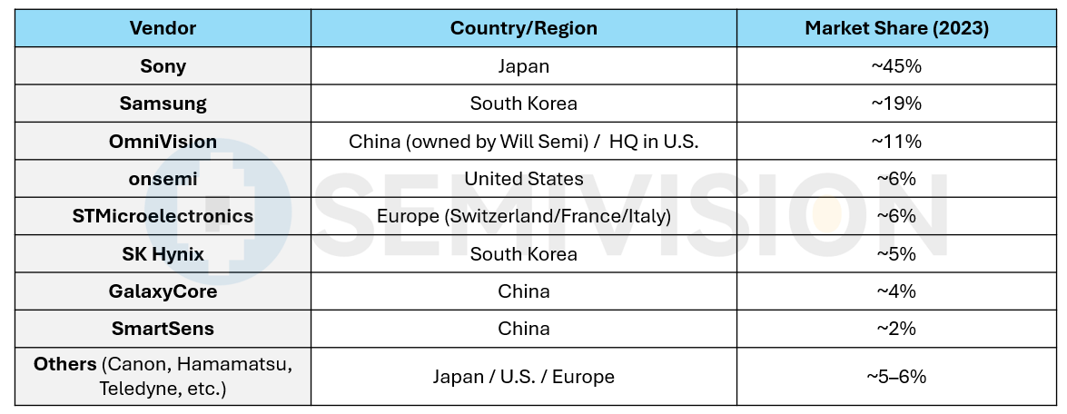
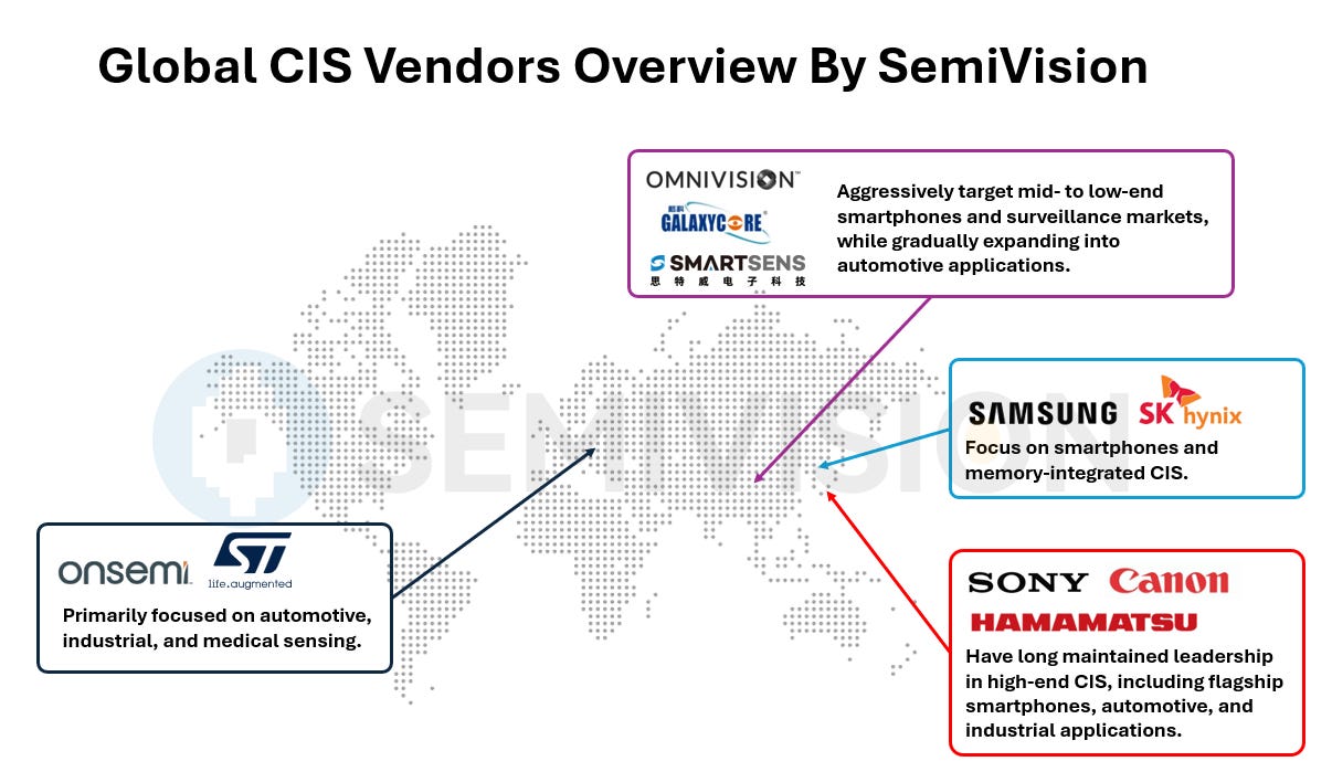
The global CIS market is dominated by three major players:Sony(leader in smartphone CIS),Samsung(ISOCELL: ultra-small pixel / high-resolution), andonsemi(automotive / machine vision), whileOMNIVISIONis rapidly catching up in smartphones and automotive.
The technology roadmap has evolved fromFSI → BSI → stacked BSI, with key enablers including:
Pixel scaling(0.56–0.6 µm class)
Deep trench isolation (DTI/ISOCELL)
Sony’s 2-layer transistor pixel(improving full well capacity and low-light performance)
HDR / LFM architectures(LOFIC, DCG)
Global shutter (GS)
On the foundry side:
TSMChas moved3-wafer stacked BSI(separating pixel / analog memory / logic) into manufacturing, integratingLOFIC × 3D-MiMinto its platform, with co-design capability alongsideN22/N12 ISPs.
UMChas mass produced300 mm BSI(down to ~1.1 µm pixel) and completedhybrid bonding / 3D-IC validation, supporting smartphone, automotive, industrial, and security applications.
The next-generation focus will be on:
Wider adoption of3-layer stacking
0.5x µm pixels + 200MP-class large-area sensors(for flagship smartphones and computational photography)
Automotive-orientedGS + LFM + HDR combos
Specialized sensors such asNIR, polarization, and event-based cameras
Close-coupled integration of sensing, logic, and memory throughW2W/D2W hybrid bonding, enabling comprehensive improvements in dynamic range, low-light performance, and system energy efficiency.
Thehistorical milestones and growth trajectoryof Sony’s CCD and CMOS image sensor business.
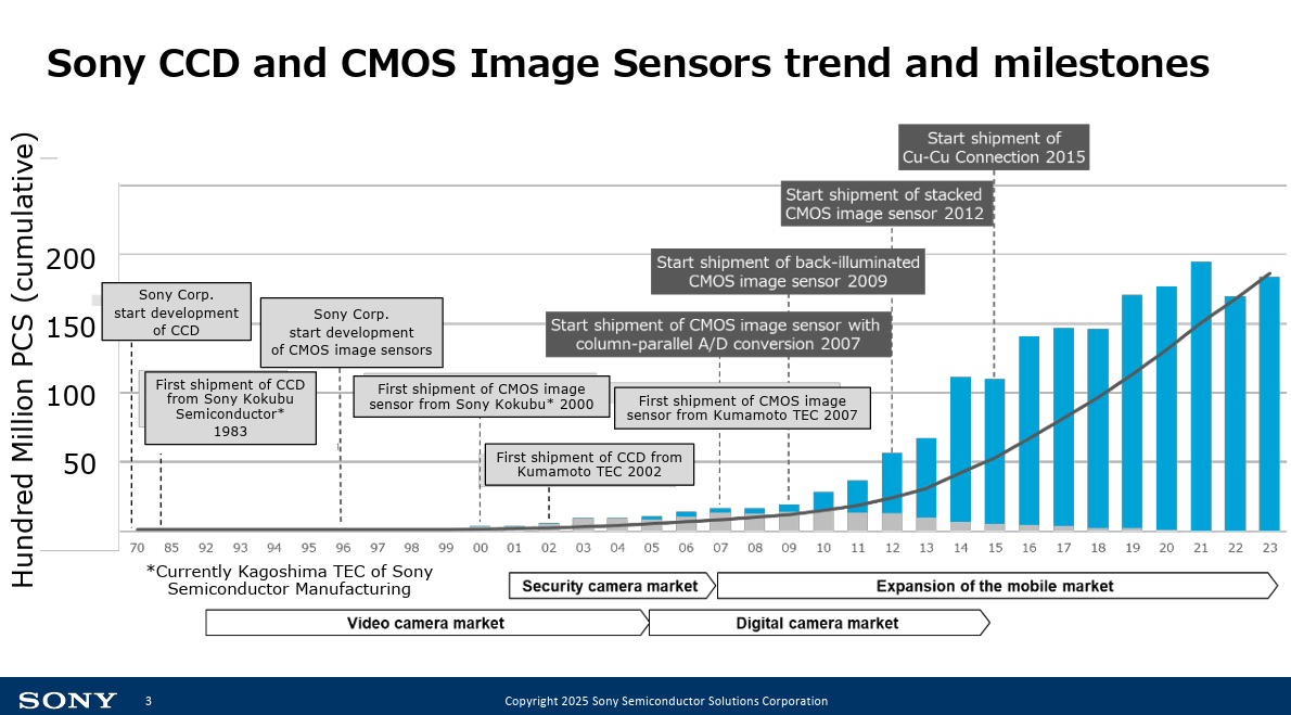
1970s–1990s:Sony began development of CCD sensors and later CMOS sensors, with the first CCD shipment in 1983 and the first CMOS shipment in 2000. During this period, the focus was mainly onvideo camerasanddigital cameras.
2000s:Sony introduced innovations such ascolumn-parallel A/D conversion (2007)andback-illuminated CMOS sensors (2009). These breakthroughs enabled performance improvements in low light and dynamic range, driving adoption insecurity camerasand digital imaging markets.
2010s:With thelaunch of stacked CMOS sensors in 2012andCu-Cu connections in 2015, Sony accelerated shipments. The market expanded rapidly beyond cameras tosmartphones, marking a sharp inflection point in cumulative unit volume.
2020s:Shipments continued to rise strongly, surpassing 200 hundred million units cumulatively by 2023, reflecting Sony’s leadership in themobile imaging marketand diversification into automotive and industrial applications.
Trend Summary:Sony’s image sensor business has shifted from early CCD dominance in video cameras to CMOS leadership in smartphones and advanced imaging. Each technological innovation—such as back-illuminated and stacked CMOS—aligned with major market expansions, driving exponential growth over the past decade.
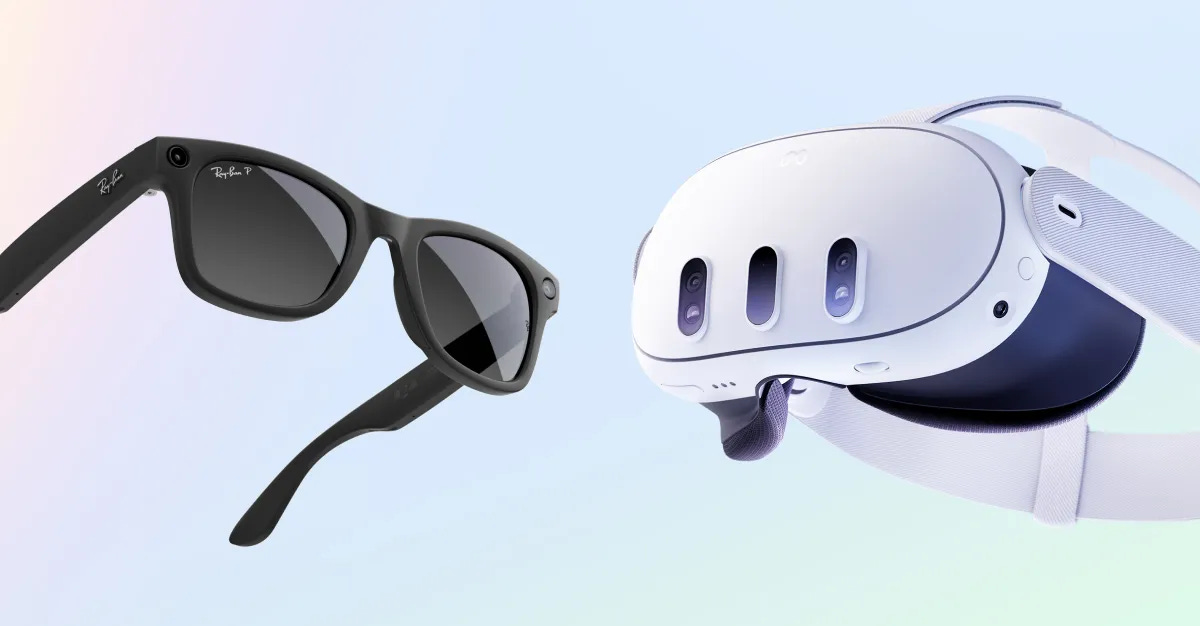
AR/VR glasses are regarded as thenext-generation human–machine interfaceafter smartphones, built on the deep integration ofoptical display, sensing chips, and edge AI computing. In principle, AR glasses usewaveguides or optical componentsto project images from micro-displays (Micro OLED / Micro LED / LCoS) into the user’s field of view. This is combined withCIS (CMOS Image Sensors)for image capture,MEMS sensors(accelerometers, gyroscopes, depth sensors) for spatial positioning and gesture tracking, and adedicated AI SoCthat processes visual and voice data locally in real time—ultimately enabling an immersive interactive experience.
Within the core chip architecture:
CIScaptures environmental and gesture images, requiring extremely high resolution, dynamic range, and low-light performance.
MEMS sensorsprovide precise head motion and spatial coordinate data, forming the foundation of spatial computing.
AI vision and voice-processing chipsserve as the edge computing engines, allowing the glasses to perform object recognition, voice interaction, and scene modeling within millisecond-level latency.
All of these chips must operate collaboratively underultra-low power consumptionand inminiaturized packaging, which is accelerating advancements inadvanced process technologies, heterogeneous integration, and 3D packaging.
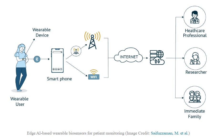
Technical Principle: The Next Generation of Human–Machine Interface
The essence of AR/VR glasses is areal-time mixed-reality platformthat integrates optical projection, sensors, and AI computing. Its operating principle is based on anoptical display module(commonly Micro OLED, Micro LED, or LCoS microdisplays), which projects images throughwaveguides or freeform opticsto overlay visuals onto the user’s field of view.
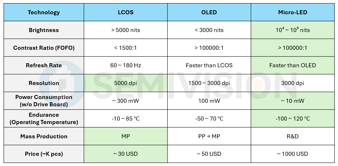
LCOS→ Best for high-resolution & cost-sensitive applications.
OLED→ Balanced choice with superior contrast but limited brightness.
Micro-LED→ Future mainstream for AR glasses, combining ultra-high brightness + low power, butnot yet commercially viabledue to cost and maturity.
To accurately align the virtual and real worlds, the glasses rely onmultimodal sensorsto collect environmental and user behavioral data, whileedge AI processorsperform rendering, fusion, and interaction within milliseconds—achieving a user experience characterized bylow latency and high immersion.
Core Chips: End-to-End Demands from Sensing to Computing
The core chip ecosystem of AR/VR smart glasses can be divided into four major categories:
CIS (CMOS Image Sensor):Acting as the “eyes,” responsible for capturing external images and gestures. Future development will rely onstacked BSI,three-wafer architectures, andhigh dynamic range (HDR)technology to support low-light environments and fast-motion scenarios.
MEMS Sensors:IncludingIMUs(accelerometers, gyroscopes, magnetometers),ToF/structured light depth modules, andoptical MEMS micromirrors, providing accurate head tracking and spatial positioning capabilities.
AI/Multimedia Processing SoCs:Integrating CPU, GPU, and NPU (neural processing unit), enabling object recognition, voice interaction, and SLAM (simultaneous localization and mapping) to deliver real-time AI computation at the edge.
Acoustic and Communication Chips:Covering microphone arrays,voice DSPs, andWi-Fi/5G/Bluetooth transceivers, ensuring natural voice interaction and low-latency connectivity.
These chips simultaneously face challenges in miniaturization, low power consumption, and heterogeneous integration, driving advancements in advanced packaging (3D stacking, fan-out, SoIC), miniaturized packaging materials, and dedicated low-power process technologies.
Industry Players: Building a Cross-Disciplinary Ecosystem
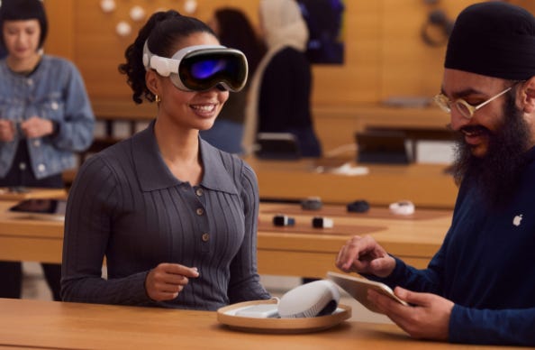
The AR/VR smart glasses industry chain spanssensors, chips, optical modules, and system brands, creating a multi-domain ecosystem:
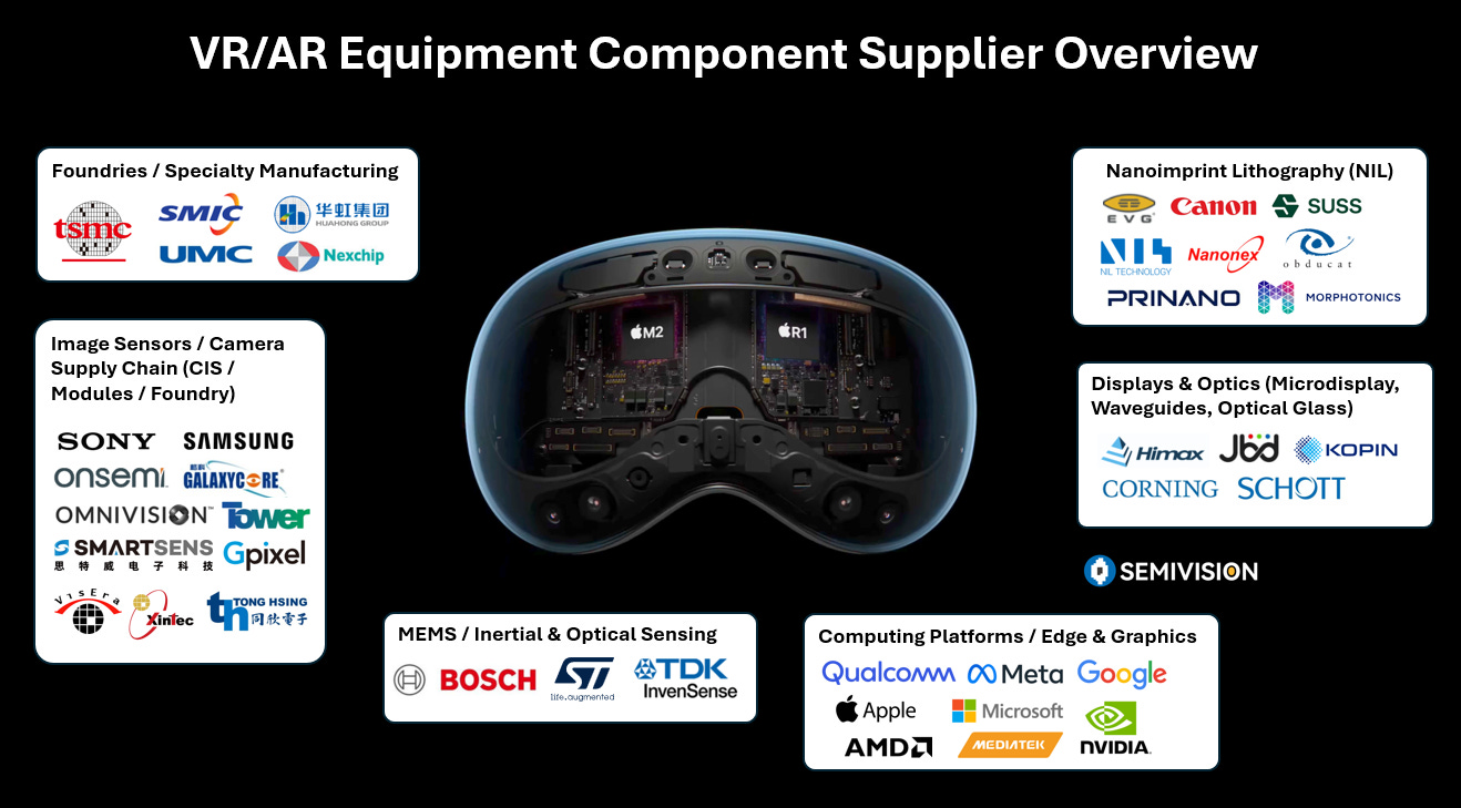
Sensors:Sony, Samsung, and OmniVisiondominate in image sensors;Bosch, STMicroelectronics, and TDK InvenSenselead in MEMS accelerometers, gyroscopes, and IMUs.
Chip Computing:Qualcomm(XR series),Apple(in-house R1/U1 chips),Meta(deep collaboration with Qualcomm), andGoogle(extending its Tensor SoC to XR) are building dedicated AI computing platforms.
Optics and Displays:Companies such asHimax, JBD, and Kopinspecialize in micro-displays and waveguides, working closely with mainstream AR device makers.
Brands and System Vendors:Apple Vision Pro, Meta Quest series, Sony PlayStation VR, Pico (ByteDance), Magic Leap, and Microsoft HoloLens—each targeting consumer, enterprise, and professional application markets.
Foundries and Platforms:TSMC and UMCare actively providingCIS, MEMS, and specialty processes, accelerating mass production and integration of sensing chips and AI computing units, thereby consolidating their positions in the wearable device market. The Kumamoto plant is TSMC’s first production site in Japan, manufacturing the country’s most advanced 12–28 nm process chips to supply customers such as Sony. Japanese companies had exited the advanced chip race in the first half of the 2000s. In the logic chip field, prior to mass production at the Kumamoto plant, Japanese fabs were only producing mature nodes such as 40 nm.
This cross-disciplinary ecosystem exemplifies apositive cycle: system vendors drive applications → chip and foundry players respond to technical demands → optics and sensor suppliers collaborate in tandem.
Edge AI Deployment: The Strategic Significance of AR/VR
AR/VR smart glasses are not just a hardware innovation—they are the frontline for Edge AI deployment. In these devices, AI models no longer rely on cloud computing but are instead directly deployed on local chips, delivering three key values:
Real-time performance:Millisecond-level latency is critical for the stability of virtual imagery, and edge computing eliminates the transmission delays of cloud processing.
Low power consumption:With dedicated NPUs and low-power process technologies, AR/VR glasses can achieve all-day operation even under limited battery capacity.
Thus, AR/VR is not only a new human–machine interface, but also acore driver for the expansion of the Edge AI ecosystem, paving the way for broad applications ranging fromsmart homes and immersive entertainment to industrial inspection, telemedicine, and educational training.

For Paid Member ,SemiVision will discuss topics on
Augmented Reality (AR) Display Principles
Meta : World-Locked Rendering (WLR)
Virtual Reality (VR) Display Principles
Meta Orion
XREAL One / One Pro (2024)
VITURE Luma Pro (2025)
Ray-Ban Meta Smart Glasses (AI Glasses)
RealWear Navigator 520 (2023–2025)
Vuzix M4000 (2021–2025)
Microsoft HoloLens 2 (2019–present)
Magic Leap 2 (2022–2025)
Meta Quest 3 (2023)
Apple Vision Pro (2024)
PlayStation VR2 (2023)
HTC Vive XR Elite (2023)
Players and Ecosystem
Major Ecosystem Platforms
Market Landscape
AR Glasses Application Analysis
Meta Orion Smart Glasses and World-Locked Rendering (WLR) Technology (Hot Chips 2025)
TSMC and the Development & Future Roadmap of AR Smart Glasses Sensing Technologies
Global CIS Suppliers and Process Evolution
Process and Architecture Evolution
Major CIS Foundry Landscape (Primarily TSMC / UMC) and Next-Generation Directions
Next-Generation CIS — A Practical Roadmap
AI Voice Technology: Positioning and Algorithmic Architecture Evolution
VisEra’s Optical Roadmap and the Fusion of Metalens Technology
Nanoimprint Lithography (NIL) × AR Glasses: Replicating Nanostructures onto Glass and Optical Films
Waveguides × AR Glasses: The Optical Backbone Delivering Images to the Eye
Supply Chain Map and Deployment Strategy: From Equipment and Materials to Design & Manufacturing
EV Group (EVG) — NIL Technology Leader
Canon — Focus on Semiconductor-Grade NIL
SUSS MicroTec (SUSS) — Multi-Purpose NIL Platforms
Global NIL Technology Supply Chain Overview
Augmented Reality (AR) Display Principles
Optical System:
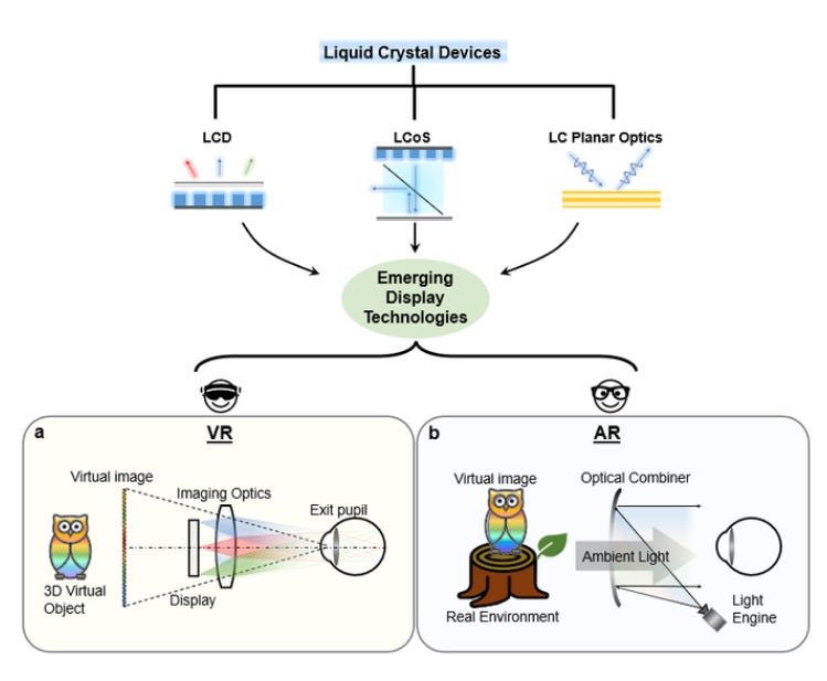
AR glasses need to project digital images onto transparent lenses without blocking the real world. A micro-display (OLED or LCD) is magnified through a lens system, then guided via coupling prisms and freeform optics to form a virtual image floating in front of the user’s eyes. Meanwhile, real-world scenes pass directly through the lenses, overlaying with the digital imagery.

To balance image quality and lightness, trade-offs are required between field of view (FOV), resolution, pupil size, and weight. Common technologies include micro-displays, waveguides, diffractive gratings, and lens arrays. For example,Magic Leap 2andHoloLens 2use glass or silicon waveguides combined with micro-display projectors, whileXREAL One ProandVITURE Luma Proemploy micro-OLED projection with prism waveguides.
Meta : World-Locked Rendering (WLR)

The core ofMeta Orionglasses isWorld-Locked Rendering (WLR), which “locks” virtual objects into the real environment so they don’t drift when the user’s head moves. According to analysis by ServeTheHome, WLR involves depth computation and synthesis, occlusion handling, audio spatialization, and demands ultra-low latency and power consumption.
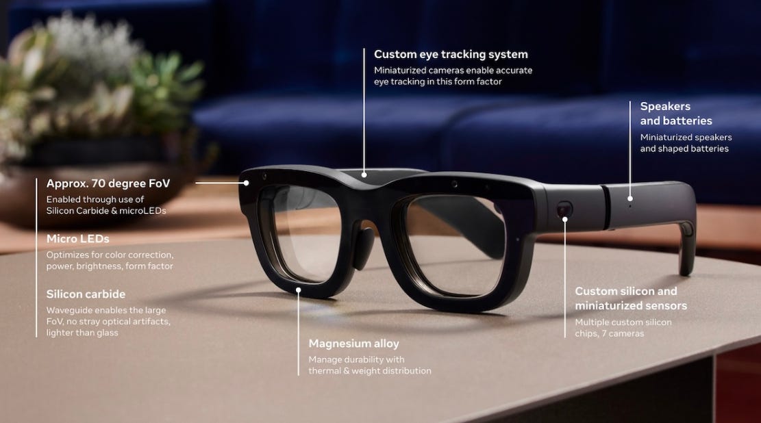
To reduce power and latency, Orion splits computation between the glasses and an external “compute puck”:
On the glasses:Two display processors (one per eye) handle reprojection and time-warp correction, each with large amounts of embedded SRAM to reduce external memory access. The main on-glasses processor manages eye- and hand-tracking as well as camera input.
On the compute puck:A large co-processor handles computer vision, machine learning, audio rendering, and HEVC codec operations.
Positioning and Tracking:
AR glasses must perceive both the user and the environment. Common components include:
Cameras and depth sensors:For example,Apple Vision Profeatures two high-resolution main cameras, six environmental tracking cameras, four eye-tracking cameras, and a LiDAR scanner.Meta Quest 3has two 4MP RGB cameras and four IR cameras, plus a depth projector for environmental scanning. These systems generate spatial maps to support gesture/eye input and occlusion.
Inertial Measurement Units (IMU):Combinations of accelerometers, gyroscopes, and magnetometers provide head orientation and motion data. Widely used in VR headsets and enterprise AR glasses (e.g.,RealWear Navigator 520integrates three IMUs).
Eye and hand tracking:HoloLens 2uses two IR cameras for eye tracking, combined with a depth sensor and SLAM algorithms for natural interaction.Apple Vision Pro’s R1 chipcan process camera and IMU data within 12 ms to update visuals in real time.
Rendering and Latency Control:
Both VR and AR devices require ultra-low latency image pipelines. Meta Orion’s WLR algorithm is highly sensitive to latency, so it uses a custom5 nm processorand specialized compression techniques to minimize memory power consumption.
XREAL One seriesuses itsX1 chip, achieving ~3 ms motion-to-photon (M2P) latency at 120 Hz refresh, far lower than theXREAL Air 2 (~20 ms)andApple Vision Pro (~12 ms).
Virtual Reality (VR) Display Principles
Stereoscopic Vision:
VR headsets create the illusion of 3D depth by presenting slightly different images to each eye. This is achieved either through two independent displays (one per eye) or by splitting a single display into left and right eye views. The difference between these images simulates binocular disparity, generating stereoscopic depth perception.
Tracking and Interaction:
VR headsets integrate gyroscopes, accelerometers, magnetometers, and internal or external cameras to track head orientation and position. With6 Degrees of Freedom (6DoF)tracking, users can move freely in a virtual space—walking, crouching, or leaning naturally. Handheld controllers add buttons, analog sticks, triggers, andhaptic feedback, allowing users to interact with the environment through gestures and tactile input.
Spatial Audio and Haptics:
Many VR systems incorporateimmersive 3D spatial audioand vibration feedback to enhance realism. Surround sound technologies simulate how sound travels in a physical environment, while haptic motors in controllers (and sometimes in gloves or vests) provide physical cues such as vibration, resistance, or pressure, amplifying immersion.
Supplementary Notes:
Latency and Refresh Rate:To maintain immersion and prevent motion sickness, VR headsets require high refresh rates (typically 90–120 Hz or higher) and very low motion-to-photon latency (~20 ms or less).
Field of View (FOV):Wide FOV (90–120°) is critical to create a natural, enveloping experience.
Eye Tracking:Advanced headsets (e.g., Meta Quest Pro, PlayStation VR2) incorporate eye-tracking forfoveated rendering, which reduces GPU load by rendering only the gaze region in full detail.
Wireless and Cloud VR:Next-generation systems are reducing reliance on wired connections, with wireless streaming and edge/cloud rendering emerging to offload compute demands while maintaining low latency.
Meta Orion

70° FOV waveguide display using silicon carbide waveguides and full-color LEDoS micro-LED projection; weight ~98 g.
The glasses house two display processors (one per eye) plus a main processor, along with a custom 5 nm silicon chip; the external compute puck contains a co-processor handling computer vision, ML, audio, and HEVC codec tasks.
Employs world-locked rendering to anchor virtual objects at low latency. Currently available only to developers; commercialization is expected post-2027.
XREAL One / One Pro (2024)

Features a 0.68-inch micro-OLED display (Pro: 0.55-inch), with FOV of 50° and 57° respectively, and a 120 Hz refresh rate; equipped with Bose audio and detachable modular camera.
Powered by theX1 chip, XREAL’s first custom AR-specific silicon (developed over three years), serving as a display co-processor enabling standalone spatial computing and 3 DoF world-locking capability.
The chip stably locks virtual screens with latency reduced to ~3 ms @120 Hz; compatible with USB-C devices.
VITURE Luma Pro (2025)

Sony micro-OLED panel providing 1920×1200 resolution and 52° FOV; peak brightness of 1000 nits.
Uses its own compute module with 3 DoF capability; through the Spacewalker app, enables world-locked and immersive 3D display.
Supports plug-and-play screen mirroring, with adjustable nose pads and built-in diopter adjustment; targeted at personal cinema and productivity applications.
Ray-Ban Meta Smart Glasses (AI Glasses)

Equipped only with camera and microphones, with no display; positioned as a generative AI interface and content creation tool (photography, live streaming, translation).
Powered by Meta’s custom chip; integrated with the Meta AI assistant, supporting multimodal input and voice control.
Launched in 2024 and quickly gained popularity, establishing the market for non-display AI glasses.
RealWear Navigator 520 (2023–2025)
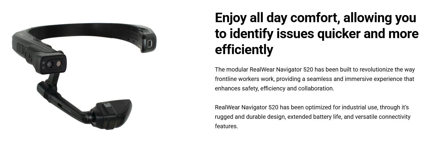
Equipped with a 0.35-inch 24-bit LCD panel, resolution 1280×720; 24° FOV; offers a 20% wider field of view and double the resolution compared to the Navigator 500.
Powered by an 8-core 2 GHz Qualcomm Snapdragon 662 processor with Adreno 610 GPU, 4 GB RAM, and 64 GB storage; includes 3 IMUs, GPS, and other sensors; built-in 48 MP camera supports stills and 1080p60 video recording.
Hot-swappable battery enables full-shift operation; ruggedized with IP66 and MIL-STD-810H certification; designed for industrial remote assistance and maintenance.
Vuzix M4000 (2021–2025)

Uses a 1 mm-thick transparent waveguide to deliver projected imagery into the eye; WVGA 854×480 DLP display with 28° diagonal FOV and brightness up to 5000 nits.
Powered by an 8-core 2.52 GHz Qualcomm XR1 processor, 6 GB RAM, and 64 GB storage; supports GPS/GLONASS, IP67 water/dust resistance, and 1 m drop protection.
Hot-swappable battery system (internal 135 mAh + external 1000 mAh) enables 2–12 hours of operation; emphasizes 3 DoF head tracking, voice control, and barcode scanning; widely used in remote support and repair.

Microsoft HoloLens 2 (2019–present)
Features 2K×2K waveguide displays (>2.5k radiants/radian); adjustable interpupillary distance; supports retinal rendering.
Runs on Qualcomm Snapdragon 850 compute platform and second-generation custom Holographic Processing Unit (HPU); 4 GB LPDDR4X memory; equipped with 4 tracking cameras, 2 eye-tracking cameras, a Time-of-Flight depth sensor, and IMU.
Supports gesture and voice control, enterprise-grade security, and 2–3 hours of battery life; primarily used for industrial training, remote collaboration, and 3D design.
Magic Leap 2 (2022–2025)
Employs LCOS microdisplay and waveguide, with a custom 14-core image processing unit supporting local dimming.
Powered by AMD 7 nm Zen 2 CPU (4 cores / 8 threads, up to 2.4 GHz) and a custom CVIP co-processor (1,700 GOP/s fixed-point, 6 vector computer vision cores, 2 machine learning cores); also integrates 6 Cortex-A55 cores and 2 MB shared cache.
Split design keeps headset weight to ~260 g, while the compute pack provides processing and power; targeted at enterprise and medical applications, with support for environmental awareness and depth scanning.
Meta Quest 3 (2023)

Dual LCD panels, 2064×2208 resolution per eye.
Uses next-generation pancake lenses, making the body 30–40% thinner than Quest 2; weight ~515 g.
Supports 90/120 Hz refresh rates.
Powered by Qualcomm Snapdragon XR2 Gen 2 processor, delivering 2× graphics performance compared to the previous generation; 8 GB RAM and 128 GB storage.
Front sensor suite includestwo 4 MP RGB cameras, four IR cameras, and a depth projector, enabling full-color passthrough and environmental scanning.
Built-in 6 DoF tracking and PC streaming; improved audio and haptics with the newTouch Plus controllers.
Apple Vision Pro (2024)

Dualmicro-OLED displayswith over 4K pixels per eye and custom lens assemblies.
TheR1 chipprocesses data from12 cameras, 6 IMUs, a LiDAR, and ambient light sensorswithin 12 ms.
Equipped with Apple’s in-houseM2 chip(8-core CPU, 10-core GPU, 16-core Neural Engine) + R1 chip; 16 GB unified memory.
Supportseye tracking and Optic ID iris authentication.
Uses an external battery pack with ~2 hours of runtime.
Premium pricing, starting at$3,500+.
PlayStation VR2 (2023)
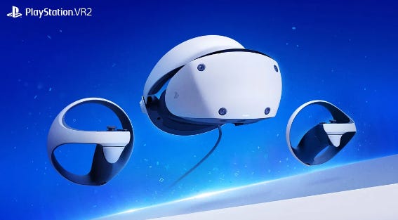
Dual4K HDR OLED panels, 2000×2040 resolution per eye, 90/120 Hz refresh rate, ~110° field of view.
UsesFresnel lenseswith interpupillary distance (IPD) adjustment.
Powered by acustom SoC co-developed with MediaTek(detailed specs not disclosed).
Inside-out tracking with four external cameras plus two eye-tracking cameras.
BundledSense controllersfeaturing adaptive triggers, haptic feedback, and finger-touch sensing.
Supportseye tracking and foveated rendering.
HTC Vive XR Elite (2023)
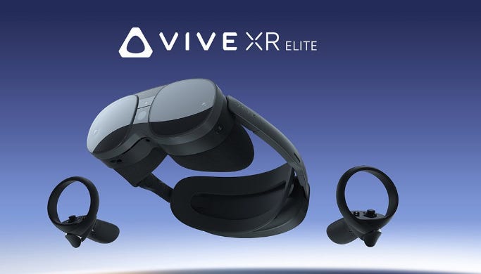
Dual LCD displays, 1920×1920 resolution per eye, ~110° FoV, 90 Hz refresh rate.
Detachable battery and modular design.
Powered byQualcomm Snapdragon XR2, with 12 GB RAM and 128 GB storage.
Equipped with a16 MP RGB camera, four tracking cameras, and a depth sensor.
Hot-swappable battery with ~2 hours of runtime.
Supports6 DoF inside-out tracking.
Players and Ecosystem
The AR/VR ecosystem is rapidly taking shape, spanning from upstream key materials, optics, and sensing components, to midstream chips, displays, and system platforms, and further to downstream applications and content service providers. This ecosystem not only brings together global technology giants such as Meta, Apple, Microsoft, and Sony, but also includes semiconductor and computing platform leaders like TSMC, Qualcomm, and NVIDIA, as well as specialized suppliers in optics and manufacturing equipment such as Corning, Schott, EVG, and SUSS. At the same time, startups like Dispelix, DigiLens, NIL Technology, and Lumus are driving innovation in waveguides, holographic optics, metalenses, and nanoimprint technologies, pushing the boundaries of AR/VR display and interaction. With the addition of content developers and cloud platforms, the overall ecosystem is evolving into a cross-disciplinary, cross-industry landscape that integrates hardware and software, computation and applications, collectively building the foundation for the next generation of immersive experiences.
Major Ecosystem Platforms
Meta Horizon OS Platform:
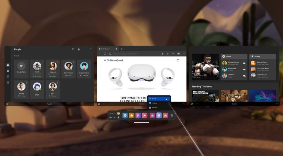
Meta has built up a large user base and content library through the Quest series. According to TS2, by 2025 Meta has licensed Horizon OS to ASUS, Lenovo, and other manufacturers to develop dedicated VR headsets. This may evolve into a multi-vendor collaboration model similar to Android. Quest 3 and the upcoming Quest 3S provide entry-level products starting at $300.
Apple visionOS Ecosystem:

Vision Pro runs on visionOS, supporting iPad and Mac apps in windowed operation. Backed by the App Store and a new spatial media format, it is positioned as a high-end "spatial computing" platform. Its high price limits adoption, but its immersive video experiences and partnerships (such as Disney+) showcase strong content potential.
Android XR Platform:

Google and Samsung’s Project Moohan mixed reality headset is expected to launch at the end of 2025, powered by the Snapdragon XR2+ Gen 2 chip. It will reportedly offer up to 4.3K resolution per eye, full-color passthrough, and eye tracking. The platform emphasizes compatibility with the Android app ecosystem and will integrate the Google AI assistant.
SteamVR / PC Ecosystem:
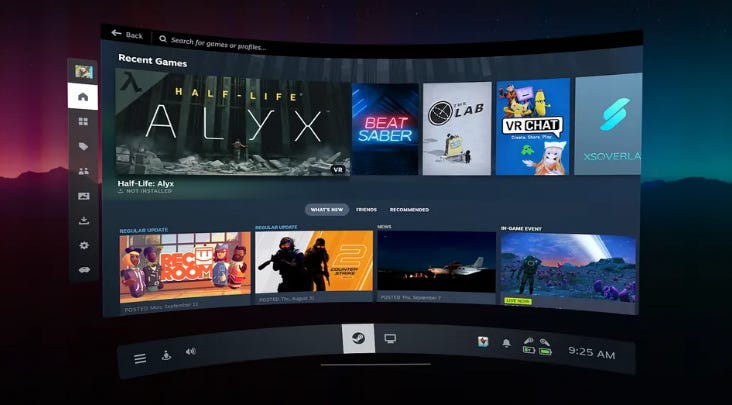
Valve’s SteamVR remains the core platform for PC VR, supporting a wide range of headsets and offering a massive library of mods and simulation games. The rumored Index 2 (Deckard) may feature a wireless design and new controllers. PS VR2 can also connect to SteamVR via a PC adapter.
Industrial Software and Services:
Devices from RealWear and Vuzix are often paired with remote collaboration software such as TeamViewer Frontline and Microsoft Dynamics Guides. They support MDM (mobile device management) and enterprise security requirements.
Market Landscape
Consumer Segment:
In 2025, the VR market is estimated to be worth around $6.7–7.0 billion, with over 1.8 million headsets in use globally. The high-end segment is led by Apple Vision Pro, the mid-range market is contested by Meta Quest 3 and HTC Vive XR Elite, and the low-end is covered by Quest 3S or continued Quest 2 shipments. Display-based AR glasses are also gaining popularity, withXREALandVITUREholding strong positions in personal cinema and mobile productivity.
Enterprise Segment:
Industrial applications show strong demand for "wearable, rugged, hands-free" devices. Products like RealWear Navigator 520 and Vuzix M4000 emphasize long-duration use and durability. Combined with remote collaboration software, they are used in maintenance, inspections, training, and logistics management.
New Entrants:
Google/Samsung’s Moohan project and Meta’s Orion are set to redefine the future of AR form factors. TS2 highlights that competition among the three major platforms—Meta, Apple, and Android XR—will become the focal point of the industry.
AR Glasses Application Analysis
- Remote Assistance and Industrial Maintenance
Smart glasses provide see-through guidance for field technicians. As described in a Wideum article, engineers can livestream through the glasses and receive real-time guidance from remote experts for maintenance, inspection, and troubleshooting. These applications reduce downtime and save travel costs. For example,ENGIEuses Iristick glasses to train field technicians, whileKUKAandAmazonuse AR glasses for equipment maintenance. The rugged design and voice control ofRealWear NavigatorandVuzix M4000make them suitable for factories, mining sites, and oil platforms.
- Training and Knowledge Transfer
AR glasses can project virtual instructions, operating steps, or 3D models, enabling learners to practice in real environments. According to Wideum, companies use AR remote training to accelerate onboarding and reduce the learning curve. In healthcare, AR glasses are used for surgical assistance and remote teaching.HoloLens 2andMagic Leap 2offer high-precision environmental sensing and gesture control, making them well-suited for medical simulation and surgical planning.
-Entertainment and Personal Cinema
Display glasses such asXREAL OneandVITURE Luma Proprovide users with a massive “personal screen.” The VITURE Luma Pro, with a Sony micro-OLED panel, offers1920×1200 resolution, 52° FOV, and 1000 nits brightness, equivalent to watching a 152-inch screen from 10 feet away. The XREAL One Pro features a0.55-inch micro-OLED display with 57° FOV. Users can watch movies, play cloud games, or connect to handheld devices like the Steam Deck. ItsX1 chipprovides 3 DoF world-locking to prevent image drift.
-Productivity and Virtual Office
AR glasses can display multiple virtual screens for document editing, coding, or data analysis. The developer edition ofMeta OriondemonstratesWorld-Locked Rendering (WLR), fixing multiple work windows in real space with AI assistant and voice input interaction.VITURE Luma Proallows three fixed surrounding screens in 3 DoF mode and supports immersive 3D display. These features are attractive to mobile professionals who need multiple monitors.
-Navigation, Translation, and AI Assistant
Smart glasses with cameras and microphones can support real-time translation, navigation, and information retrieval.RokidandSoloshave released micro-LED glasses with translation subtitles.Ray-Ban Meta glassesintegrate the Meta AI assistant, enabling voice-based queries, foreign language translation, and first-person short video recording. With the rise of large language models and cloud computing, glasses are evolving into a keyAI interface.
- Consumer Retail and Demonstration
Retailers use AR glasses to offer virtual try-on, product guidance, and in-store navigation. Customers can see virtual outfits or product information directly through the glasses, enhancing the shopping experience. Similarly, real estate agents use AR glasses to allow clients to visualize virtual furniture or interior designs on-site. These applications require high-precision positioning and realistic occlusion, which depend on technologies like WLR.
- Future Outlook
Micro-LED and LEDoS Displays:Meta Orion’s full-color LEDoS micro-LED technology offers high brightness and compact size, but current costs are high and waveguide resolution remains limited. Consumer-ready products are expected around2026–2027.
6 DoF and Environmental Awareness:Most current display glasses support only 3 DoF, butVITUREandXREALare developing 6 DoF tracking. Future devices will integrate depth cameras and SLAM algorithms for full spatial computing and persistent positioning.
Split Compute and Cloud:To reduce headset weight, many AR devices adopt a split architecture.Meta OrionandMagic Leap 2use external battery/compute packs. With advancements in cloud rendering and edge computing, glasses may further evolve into lightweight display terminals.
Platform Competition and Standardization:Starting in 2025,Meta, Apple, and Google/Samsungform the three dominant platforms. Ecosystem richness and application content will shape the market landscape. Open standards likeOpenXRare already driving cross-platform development.
AR/VR glasses are transitioning from prototypes to practical tools. World-Locked Rendering (WLR), micro-displays, waveguide optics, and artificial intelligence are the key driving technologies. Meta Orion leverages custom silicon and split computing to achieve 70° FOV and low-latency WLR; XREAL and VITURE target personal cinema and mobile productivity with lightweight display glasses; while RealWear and Vuzix focus on industrial remote collaboration. In the coming years, as Micro LED costs decline, 6 DoF tracking becomes mainstream, and AI assistants are integrated, AR glasses will evolve from auxiliary tools into intelligent terminals that seamlessly support work, production, entertainment, and learning.

Meta Orion Smart Glasses and World-Locked Rendering (WLR) Technology (Hot Chips 2025)
-WLR Technology Principles and Architecture: Creating an Immersive Mixed-Reality Experience
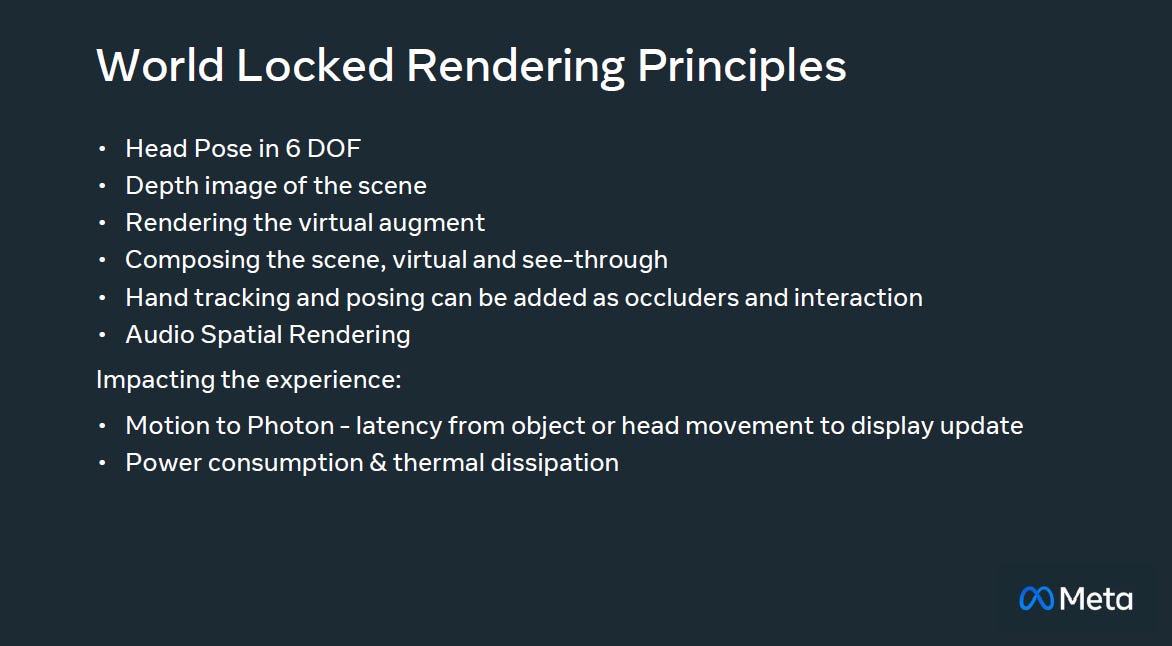
Meta’s Orion smart glasses useWorld-Locked Rendering (WLR)as the core technology to achieve seamless blending of real and virtual imagery. WLR involves six key steps:
Head pose capture (6DoF)
Scene depth map construction
Virtual content rendering
Real/virtual image composition
Hand tracking and gesture recognition
Spatial audio synchronization

The overall architecture spans frominput (IMU, cameras, depth sensors)→compute (depth processing, virtual rendering, audio processing)→output (real/virtual composition and display), forming a tightly integrated closed-loop system. Key performance metrics aremotion-to-photon latencyandpower/thermal efficiency, which determine immersion and comfort, requiring full-stack hardware optimization.
-Custom Chip Design: Breakthroughs in Power, Size, and Sustained Compute
To support continuous WLR operation, Meta developedthree dedicated processorsfor Orion, each handling data collection, image display, or compute-intensive tasks. The three major optimization strategies are:
Power Control:5 nm advanced process, minimized DRAM usage, data compression, low-voltage/high-frequency operation, and DVFS (dynamic voltage and frequency scaling).
Size Integration:System-in-Package (SiP) to reduce interconnects and shrink module size for eyewear miniaturization.
Sustained Operation:Decentralized control and modular activation to support long-duration workloads with low latency and flexible scalability.
Among the three processors:
Theeyewear processorhandles image input and tracking, integrating eye-tracking and gesture accelerators.
Thedisplay processorstabilizes visuals with reprojection algorithms to reduce dynamic latency.
Thecompute co-processorprovides SLAM, VIO, CV, ML, and audio rendering, serving as the compute hub with5.7 billion transistors.
-Orion System Integration: Distributed Collaboration of Glasses + Wrist Puck
Orion is not a single device but a distributed system composed ofsmart glassesand awrist controller (“Wrist Puck”). The Wrist Puck connects via Wi-Fi/Bluetooth, providing interaction and sharing compute/control workloads. Its advantages include:
Modular separationfor flexible use and convenience.
Power partitioning, with independent power domains for the three processors and energy-efficient wrist design to extend battery life.
Synchronized data and real-time rendering, with high-speed wireless links preventing misalignment or lag in visual/audio output.
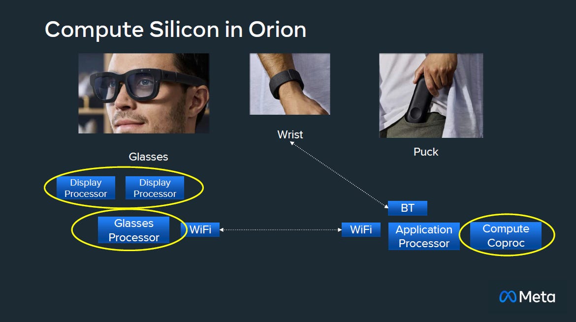
Orion demonstratesend-to-end innovationfrom rendering technology to chip design and product integration. It sets a technical benchmark for consumer-grade AR/MR devices and highlights Meta’s strategic leadership in wearable computing.
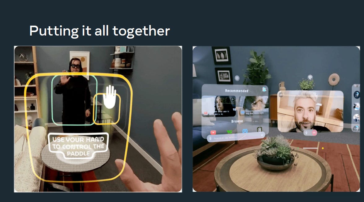
TSMC and the Development & Future Roadmap of AR Smart Glasses Sensing Technologies
TSMC’s Strategic Position in Sensor Technologies
As Augmented Reality (AR) technology gradually enters the consumer market, the importance of sensors is steadily increasing. If processors are the “brain” of smart glasses, then sensors are the “eyes and ears,” determining whether the device can accurately perceive its surroundings and deliver a stable, immersive experience.
As the world’s leading foundry,TSMCnot only has a strong advantage in advanced logic processes but is also actively expanding into the sensor field. At itsNorth America Technology Symposium, TSMC explicitly stated:
“Sensor Technologies: CIS (CMOS Image Sensors): Fabricated on N22/N45 to support high-resolution environmental sensing and surround vision.”
This statement reveals two key messages:
CIS (CMOS Image Sensors)are a fundamental building block for AR devices.
TSMC is already leveraging its dedicated22nm and 45nm nodesto deliver high-resolution CIS solutions, supporting environmental sensing and surround vision in AR systems.
CIS technology offers high resolution, low power consumption, and fast capture speeds—ideal for miniaturized, wearable AR devices. With multiple CIS modules embedded, smart glasses can capture multi-directional imagery and, combined with software algorithms, reconstruct a3D model of the environment. This forms the foundation for accurate virtual image overlay. Since AR experiences demandlow-latency real-time rendering, even minor frame delays or jitter degrade immersion. Therefore, CIS readout speed and power efficiency are critical performance indicators.
TSMC’s participation in this field means that beyond being an AI chip foundry partner, it is also becoming akey enabler of smart sensing solutions.
Global CIS Suppliers and Process Evolution
Currently, major global CIS suppliers includeSony, Samsung, onsemi, and OmniVision, among others. At the same time, foundries such asTSMC and UMCare actively positioning themselves as next-generation CIS manufacturers.
1) Global CIS Market Share Dynamics (2024–2025)
Smartphone CIS Market (the core sub-market):
Throughout 2024, Sony maintained the No.1 position with>50–55% sharein smartphone CIS. Samsung System LSI ranked second, and OmniVision third, with quarterly variations.
Industry Scale:
Research firms project the CIS market will surpassUSD 30 billion by 2030. After modest growth of ~6–10% YoY in 2024, revenues are rebounding. Sony remains the industry leader overall.
Geographic Breakdown (2024):
China: ~19% (OmniVision, SmartSens, Gpixel, etc.)
Japan: ~48% (dominated by Sony)
Korea: ~21% (dominated by Samsung)
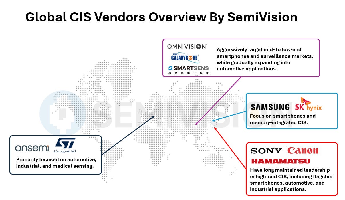
Automotive CIS:
According to TechInsights, OmniVision claimed>30% share in automotive CIS in 2024, overtaking onsemi, which had been long dominant. This indicates rapid reshuffling in the automotive segment, with competition intensifying.
Supplier Strategies in CIS
Sony:Continues to lead with stacked BSI architectures, multiple-layer pixel designs, and pushing high-performance imaging across mobile and beyond.
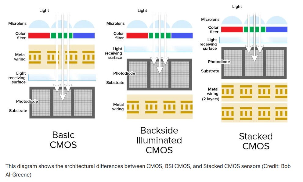
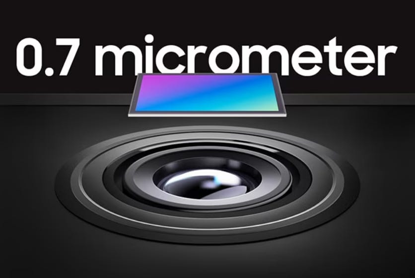
Samsung:Advances itsISOCELLbrand withultra-small pixels (0.7 µm, HP2/HP3 200MP), and innovations in pixel isolation, pixel binning (Tetra^2pixel), and low-light computational algorithms.
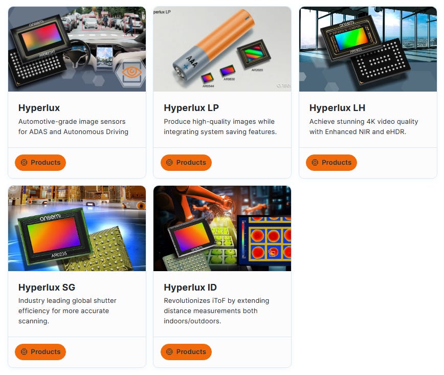
onsemi:Focuses on itsHyperlux familyfor automotive/machine vision, emphasizingglobal shutter, LED flicker mitigation (LFM), and high dynamic range (HDR).
OmniVision:Actively promotesTheiaCel™ technology(low-light and anti-glare), alongside high-resolution stacked pixel innovations down to0.56 µm.

At GTC 2024, OMNIVISION will demonstrate its OX08D10 image sensor on NVIDIA Omniverse, a platform of APIs, SDKs and services for 3D applications such as autonomous vehicle simulation
In short,TSMC’s entry into CIS manufacturing aligns with global AR demand for advanced sensors. With CIS evolving towardstacked architectures, ultra-small pixels, HDR, and LFM, the collaboration between foundries (TSMC, UMC) and device suppliers (Sony, Samsung, onsemi, OmniVision) will shape the future of AR smart glasses—whereprecision sensing is just as critical as AI computing power.
Process and Architecture Evolution
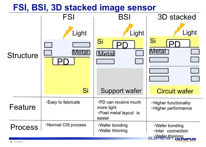
FSI → BSI → Stacked BSI:
CIS technology has shifted from front-side illumination (FSI) to back-side illumination (BSI). Two-wafer stacking (pixel layer + logic layer) is now widely adopted, with the industry moving further towardthree-wafer stacking(e.g., pixel + analog/memory + logic).TSMC has already transferred three-wafer stacked BSI into mass production.
Sony’s “2-Layer Transistor Pixel”:
Separates pixel transistors and photodiodes into different layers and then stacks them, significantly improving full-well capacity and low-light performance (publicly announced by Sony in 2021).
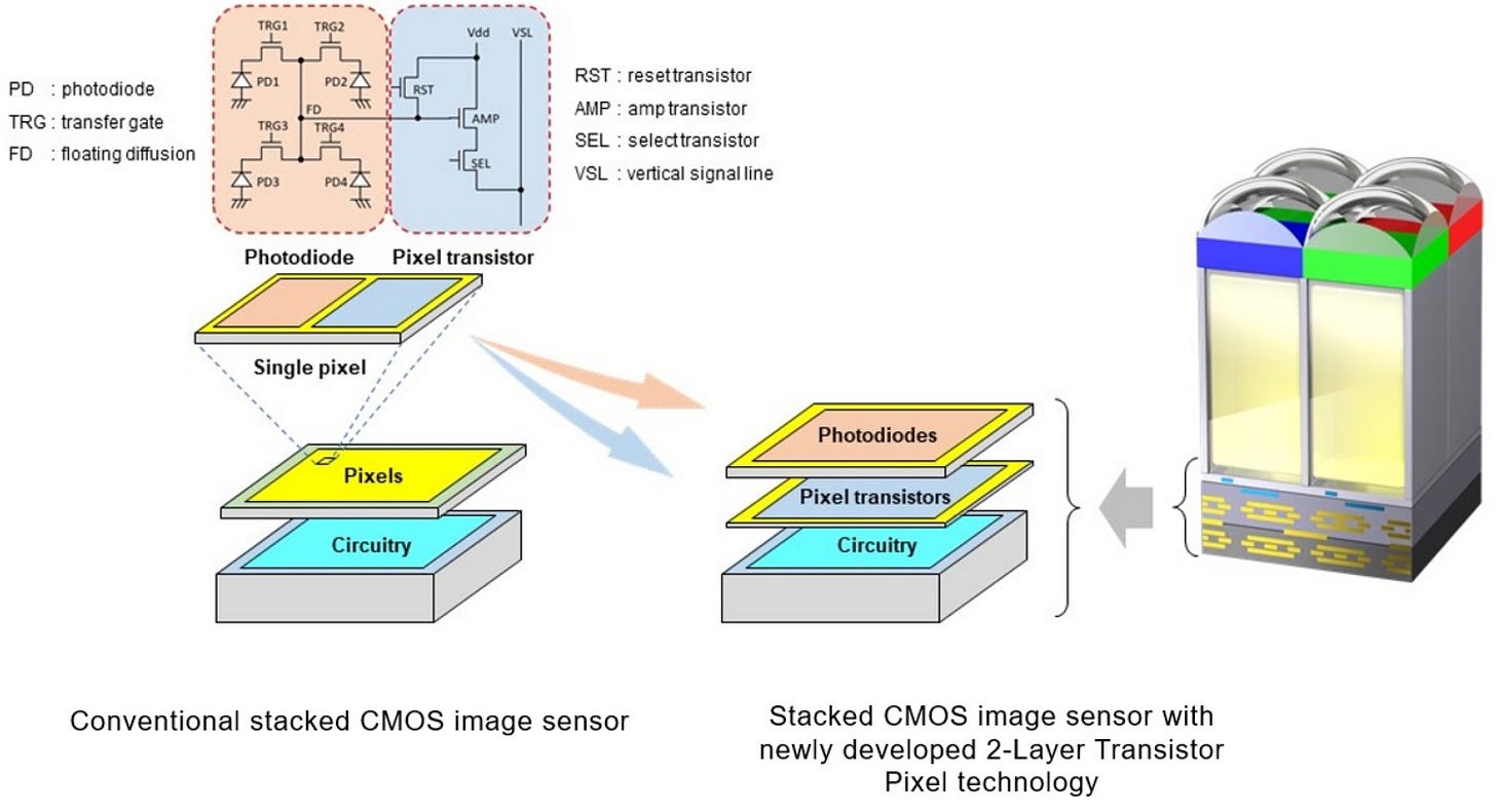
Source: sony
Pixel Scaling and Isolation:
ISOCELL/DTI (Deep Trench Isolation)and material/structural optimizations support pixel sizes down to0.6 µm and below. Multi-in-one pixel binning (Quad/Tetra/Hexa) improves SNR and low-light dynamic performance.
HDR and LFM:
Implemented through multi-reset,dual conversion gain (DCG), andLOFIC(often combined with 3D-MiM). TSMC’s published data shows that3D-MiM LOFIC improvements can deliver ~14 dB performance gain.
Global Shutter:
Achieved via pixel charge storage or stacked capacitors with low-leakage design. Rapid adoption in industrial and automotive applications.Toweralso offers a65 nm BSI GS platform and IP.
Emerging Directions:
Technologies such asevent-based/neuromorphic cameras, metasurface optics, and curved sensorsare expanding the application frontier.
Major CIS Foundry Landscape (Primarily TSMC / UMC) and Next-Generation Directions
TSMC (CIS and Specialty Technology Platform Integration)
3-Wafer Stacked BSI:Alreadytransferred to manufacturing. By optimizing and stacking pixel, analog/memory, and logic tiers, this architecture improves dynamic range, noise performance, and functional integration.
LOFIC × 3D-MiM:TSMC reported that improvements in LOFIC (Lateral Overflow Integration Capacitor) combined with 3D-MiM yield ~14 dB performance gains.
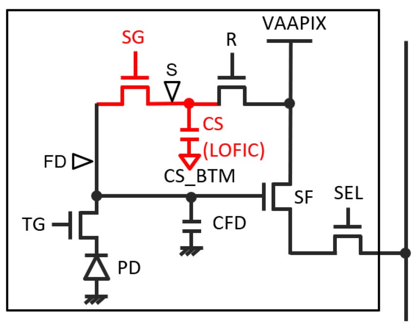
Pixel circuit schematic of a lateral overflow integration capacitor (LOFIC) pixel.
Integration with Advanced ISP Nodes:TSMC emphasizes the co-optimization of CIS/ISP with advanced low-power logic at N22 and N12, which is critical for mobile, automotive SoCs, and highly integrated modules.
Official Technology Pages:TSMC’s CIS webpage clearly lists BSI, W2W stacking, advanced pixel/packaging capabilities, and platformized services.
Technology Forum Context:Although the 2025 TSMC Technology Symposium centered on AI and packaging, post-event materials and the official site also highlightedsensing and specialty technologiesas strategic platforms.
Industry Chain Connections:OMNIVISION has long relied on TSMC for wafer foundry, with VisEra handling BSI/color filter/packaging — a classicfabless + foundry + OSATmodel.
UMC (Mature Nodes, BSI, and 3D Connectivity)
300 mm BSI Platform:UMC offers 200 mm FSI and 300 mm BSI solutions with pixel sizes down to 1.1 µm, targeting smartphones, automotive, security, and industrial control.
Historical Cooperation and Evolution:UMC collaborated with ST on a 65 nm BSI (1.1 µm pixel) as an open platform at Fab12i (Singapore). Later, UMC continued expansion in 22/28 nm logic, including ISP support.
3D/Hybrid Bonding Capabilities:Together with Cadence, UMC demonstrated 40 nm hybrid bonding 3D-IC verification, establishing EDA/process linkage for stacked CIS customization — critical for next-gen architectures.
Other Foundry and IDM Players
Samsung:Predominantly in-house (IDM/System LSI + Samsung Foundry). Pursues ISOCELL roadmap (0.6 µm, 200MP, Tetra^2pixel pixel-binning).
Sony:Primarily IDM/in-house production, pushing2-Layer Transistor Pixeland multiple stacked architectures.
Tower Semiconductor:Provides 65 nm BSI/Global Shutter platform and IP, focusing on industrial and automotive applications.
SMIC / HHGrace / Nexchip (China):Provide mature-node foundry services for CIS/DDI. In 2025, SmartSens and Nexchip announced a long-term strategic partnership, underscoring China’s efforts to vertically integrate CIS supply chains.

Next-Generation CIS — A Practical Roadmap
Three-Layer Stacked Mass Production (Pixel / Analog-Memory / Logic Partitioning)
→ TSMC has alreadytransferred to manufacturing. OMNIVISION and top-tier smartphone makers are potential early adopters. Automotive applications, particularly those requiring high HDR and low-light performance, will also benefit.
0.5x µm-Class Pixels + Large-Area, High-Pixel Sensors
→ Samsung ISOCELL continues to push 0.6 µm pixels to the limit with pixel binning optimization; Sony leverages stacked transistor pixel architectures to improve low-light and dynamic range.
HDR/LFM New Structures (LOFIC × 3D-MiM, DCG Multi-Mode)
→ TSMC has demonstrated ~14 dB performance gains. Automotive and machine-vision applications are the most immediate beneficiaries.
Global Shutter + NIR/Polarization/Multi-Spectral
→ Tower Semiconductor and multiple industrial/automotive supply chains are developing standardized process and pixel IP platforms, enabling faster customization.
Event Cameras / Neuromorphic & Metasurface Optics
→ Still accelerating toward commercialization, with initial adoption in industrial, surveillance, and robotics (per Yole’s perspective).
AI Voice Technology: Positioning and Algorithmic Architecture Evolution
- Voice as the Core of Human–Machine Interaction
In the evolution of human–machine interfaces, keyboards and mice were once dominant, followed by touchscreens becoming the most intuitive interaction after the rise of smartphones. However, as devices and use cases multiply, users now expect a morenatural, intuitive, and spatially unconstrainedinteraction mode. Against this backdrop,voice has emerged as a key interaction paradigm.
The primary advantages of voice are itslow barrier and high intuitiveness. Speaking is faster and more natural than typing, and it overcomes the limitations of visual or manual interaction. For example, during driving when touch is unsafe, voice commands improve both safety and convenience. On lightweight devices like wearables or smart glasses, voice is the most natural input method.
Yet for voice to be truly practical, challenges go beyond simply “recognizing human speech.” Systems must:
Capture speech accurately in noisy environments
Process data in real-time under limited device compute and power budgets
Leverage language models for semantic understanding
Respond withnatural-sounding voice output
This requires afull-stack algorithmic and architectural pipeline— from front-end sensing, signal processing, and language understanding to back-end speech synthesis.
- Algorithm-Driven Audio Processing Logic
(a) From Hardware to Algorithmic Intelligence
Traditional microphone arrays or directional microphones relied on physical design to reduce noise. As devices become thinner and more power-constrained, hardware alone is insufficient. The introduction ofAI algorithmshas transformed voice processing:
Speech/Non-Speech Separation:Deep learning networks can isolate human voice signals from complex soundscapes with high accuracy, even in cafés, cars, or outdoor environments.
Noise Suppression & Echo Cancellation:Algorithms identify background noise patterns and proactively filter out interference such as keyboard clicks, fans, or other voices.
Voiceprint Recognition:Converts speech into unique biometric features for authentication, preference detection, and personalized experiences.
(b) Layered Architecture: Perception, Understanding, Response
Perception Layer:Converts analog sound into clean, usable digital signals. Requires highly efficient signal processing, especially on low-power platforms.
Understanding Layer:Processes digital signals through language models for semantic analysis and command interpretation. Key challenge: balancing model size, inference accuracy, and resource efficiency.
Response Layer:Uses speech synthesis to transform system feedback into natural, fluent, and emotionally expressive voice output.
This modular “building block” design allows algorithms to be flexibly configured across different devices and scenarios, enabling scalable deployment ofAI voice interfacesin smart glasses, wearables, and other platforms.
Next-generation CIS will be driven bystacked architectures, ultra-small pixels, HDR/LFM, and specialty imaging (GS, NIR, multi-spectral, event cameras). In parallel,AI voice technologyis evolving as the most natural form of interaction for lightweight AR/VR devices, requiringend-to-end algorithmic innovationacross sensing, understanding, and response layers.
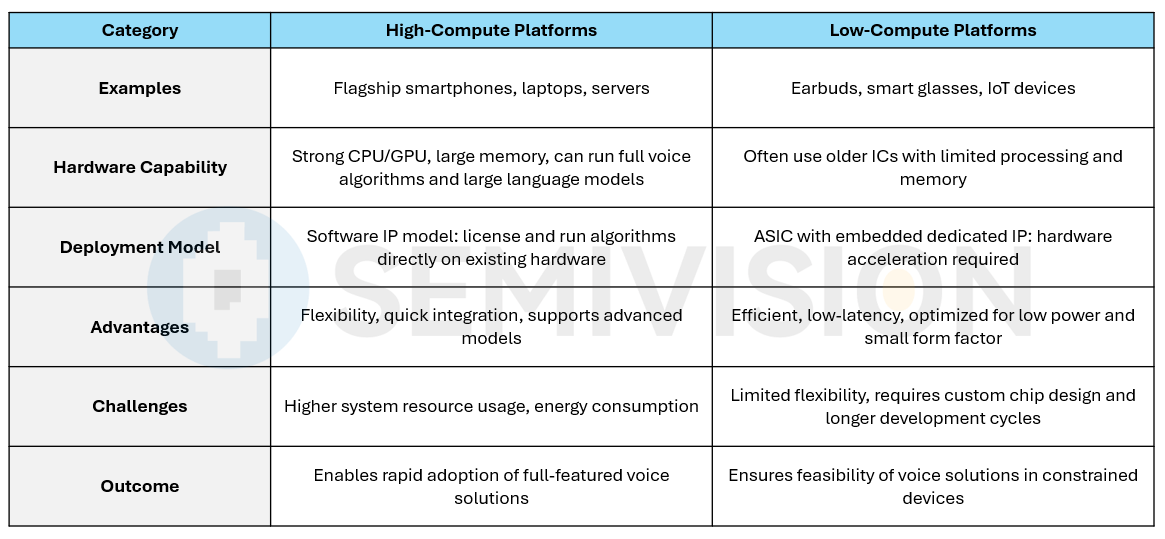
- Differences in Platform Compute Power and Solutions
Whether voice algorithms can be successfully deployed depends heavily onplatform compute capability, which varies significantly across devices and presents major challenges for algorithm design.
High-Compute Platforms:
Devices such as flagship smartphones, laptops, or servers can directly run complete voice algorithms and large language models. On these platforms, voice technology is typically delivered in anIP model—software algorithms are licensed and executed within the customer’s existing hardware and OS environment.
Low-Compute Platforms:
Devices such as earbuds, smart glasses, or IoT terminals often rely on ICs designed years ago and may lack support for modern, compute-intensive algorithms. In these cases, solutions requireASIC chips with embedded dedicated IP, using hardware acceleration to boost efficiency while minimizing latency and power consumption.
Comparison:
High-compute platforms enableflexibility and rapid deploymentof advanced voice algorithms but at the cost of higher system resources.
Low-compute platforms demandhardware-level innovation(ASIC + IP integration) to deliver real-time voice performance under strict energy and size constraints.
This“dual-track model” of IP and ASICensures that voice technology can scale across a wide variety of device platforms, overcoming compute limitations and enabling broad adoption.
- The Value of Modularity and Replicability
One of the biggest challenges of voice technology is the wide diversity of end-device use cases. If every device required a fully customized algorithm, the ROI (return on investment) would be unsustainable.
Thus,modularityandreplicabilitybecome core strategies:
Modularity:Break algorithms into independent building blocks, such as anoise suppression module,voiceprint recognition module, andspeech synthesis module. Customers can freely combine modules based on their needs, quickly creating suitable solutions.
Replicability:Once an algorithm module is validated on one platform, it can be quickly replicated to others with only minor adjustments.
This architecture not only reduces deployment costs but also makes large-scale commercialization of voice technology feasible.
- Voiceprint and Natural Language Models
Beyond traditional speech recognition, the future of voice interaction emphasizespersonalizationandnatural dialogue:
Voiceprint Recognition:Allows devices to identifywhois speaking. This enables identity verification and personalized responses based on user preferences.
Natural Language Models:The next step after voice input is semantic understanding. Traditional systems rely on fixed commands, but natural language models can interpret flexible semantics and support more complex interactions.
However, general-purpose language models demand massive compute resources, making them unsuitable for all devices. Thus,lightweight modelsare the trend:
Domain-Specific Models:Compact models tailored for automotive, earbuds, or smart glasses, focusing on limited semantic ranges to reduce memory and compute needs.
ASIC + Algorithms:Hardware acceleration enables low-power devices to run simplified language models with improved responsiveness and efficiency.
- From “Voice” to a “Voice Interaction Ecosystem”
The evolution of AI voice technology is not just about signal processing algorithms, but about building acomplete ecosystem for voice interaction:
Voice Cleaning:Ensuring the device correctly hears the human voice.
Language Understanding:Enabling devices to comprehend commands and context.
Natural Response:Allowing devices to reply in a fluent, human-like manner.
This three-step closed loop makes voice the truecore of human–machine interaction. With the spread of smart glasses, automotive platforms, and robotics, voice will surpass human-to-human communication needs and become the mainstream mode for human–machine interaction.
The evolution of AI voice algorithms marks anew era of HMI (Human–Machine Interaction). From early reliance on microphone hardware, to today’s deep learning-driven speech separation and voiceprint recognition, and now the integration of natural language models for all-scenario interaction—voice is no longer just an input method, but theprimary sensory channel of smart devices.
Differences in compute capability across platforms have driven thedual-track strategy of IP + ASIC, while modularity and replicability ensure scalable deployment. As lightweight language models mature and hardware acceleration converges, voice interaction will becomeubiquitous.
Ultimately, the advancement of AI voice technology will not only transform device operation but also reshape the entire ecosystem of human–machine interaction, establishingvoice as the true gateway to future smart living.
VisEra’s Optical Roadmap and the Fusion of Metalens Technology
VisEra, a subsidiary of TSMC, has long specialized in image sensors and optical components, and in recent years has extended its focus to thecore optical modules required for AR and MR (Mixed Reality)devices. Among its R&D directions, the most noteworthy is the integration ofMetalens technologyintoCMOS Image Sensors (CIS)andMicro-Optical Elements (MOE).
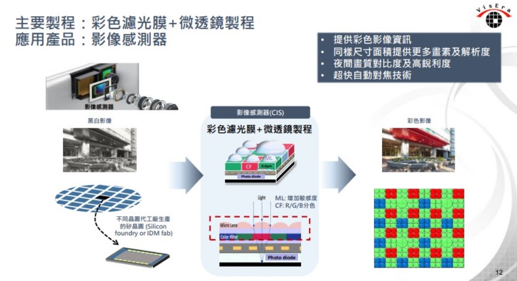
Unlike traditional lenses, which rely on curved refraction or reflection to focus light, Metalens usesnanoscale structuresto manipulate light in a flat form factor. This approach significantly reduces optical module thickness while improving light-focusing efficiency and image quality—ideal for miniaturized devices such as smart glasses, where bulky lenses add size, weight, and reduce comfort for long-term wear.
This innovation delivers multiple advantages:
Thinner and lighter AR modules, solving the common “bulky feel” problem of traditional AR devices.
Deep integration with CIS, embedding optical control directly onto the sensor surface, reducing the need for additional lens components and lowering both power consumption and latency.
Flexibility via Metalens + MOE integration, enabling adjustable optical parameters for different AR use cases—such as industrial inspection, medical assistance, or entertainment.
For TSMC, this is not only an extension of process capability but also astrategic move from semiconductor manufacturing into optical modules, showcasing its ambition to penetrate the AR ecosystem comprehensively.
Microlens technology has also been applied to TSMC’s Optical Engine. Publicly available technical information clearly shows that the Silicon COUPE architecture integrates a Microlens Array design to enhance optical coupling and overall performance.
ToF Modules and Eye-Tracking Applications
Another crucial aspect of AR experiences iseye tracking. The core function is to capture the user’s pupil position and gaze direction in real time, aligning virtual imagery perfectly with human vision. VisEra’s roadmap highlights the adoption ofTime-of-Flight (ToF) modulesto support this function.

By emitting light pulses and measuring the return time, ToF delivershigh-precision depth information. Integrated into AR glasses, ToF can measure the relative position between the eye and the optics, enabling accurate eye-movement detection.
The application value is significant:
Display accuracy:Ensures virtual objects remain anchored to real-world positions, eliminating the “floating” effect caused by head or eye movement.
Performance efficiency:Enablesfoveated rendering, where only the gaze area is rendered in high resolution while peripheral vision is downscaled, reducing compute and power consumption.
Natural interaction:Transforms the eyes into input interfaces—users can interact simply by looking, bringing revolutionary intuitiveness to AR.
TSMC and VisEra’s investment here positions them to enhanceperformance, user experience, and power efficiencyin AR systems.
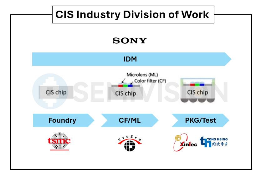
The CMOS Image Sensor (CIS) industry operates under a highly specialized division of work, where different players take on distinct roles in the value chain:
IDM (Integrated Device Manufacturer):
Companies likeSonydesign and integrate the CIS chip, handling the overall system and technology development.
Foundry:
TSMCprovides advanced wafer manufacturing for CIS chips, leveraging its specialty process nodes.
CF/ML (Color Filter & Microlens):
VisErafocuses on applyingcolor filters (CF)andmicrolenses (ML)to enhance image quality and light sensitivity.
PKG/Test (Packaging & Testing):
Companies such asXintecandTong Hsingspecialize in advanced packaging and final testing of CIS devices, ensuring performance, reliability, and readiness for integration into end products.
This ecosystem exemplifies thefabless–foundry–OSAT collaboration model, allowing each partner to focus on its core strengths while jointly driving innovation and mass production in the CIS industry.
Integration Trends and Future Outlook
Taken together, TSMC and VisEra’s roadmap outlines acomplete blueprint for future AR smart glasses:
CIS sensorsdeliver precise environmental image capture.
ToF modulesenable eye tracking and depth sensing.
Metalens and MOEsprovide a lightweight, high-performance optical foundation.
Combined withmicro-OLED or Micro-LED displays, these technologies create a system defined bycompact size, low power, and high immersion.
Importantly, TSMC is not just acting as a foundry—it is building avertically integrated value chainthat spans wafer process, optical modules, and system applications, in collaboration with ecosystem partners.
The AR market’s potential goes well beyond gaming or entertainment. Industrial manufacturing, medical diagnostics, education, and remote collaboration are among the domains poised for transformation. By advancing Metalens, ToF, and CIS into maturity and mass production,TSMC is positioning itself as a foundational enabler of the entire industry.
From this perspective, devices likeMeta’s Orionare only thefirst step toward mainstream adoption. Over the next 5–10 years, as processes advance and optical materials continue to improve, AR smart glasses are likely to become amainstream terminal on par with smartphones—with TSMC serving as anindispensable technology driverbehind this shift.
Nanoimprint Lithography (NIL) × AR Glasses: Replicating Nanostructures onto Glass and Optical Films
UV-based Nanoimprint Lithography (UV-NIL)adopts a“master → replica stamp → mass-production imprinting”process flow, enabling nanostructures to be quickly replicated onto glass or resin films. This approach provides large-area coverage, high throughput, repeatability, and low unit cost, directly addressing the mass-production challenges of AR waveguides.
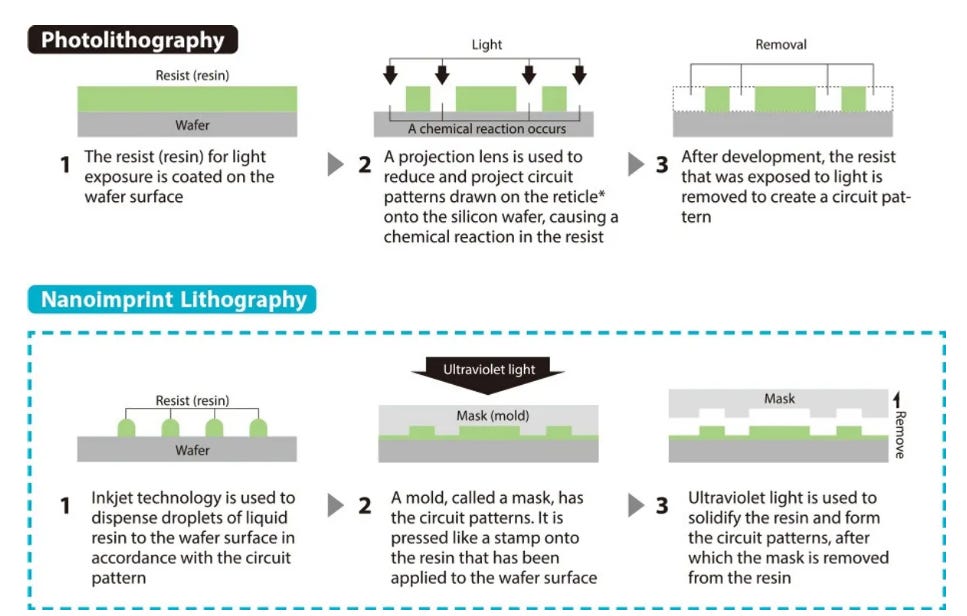
Source: Canon
Production Platforms:
Full-field SmartNIL:Designed for large-area, wafer-level, and wafer-level optics (WLO) stacking.
Step-and-repeat NIL:Uses stepper imprinting and high-precision alignment to stitch nanostructures across the entire substrate, achieving resolutions down to tens of nanometers—ideal for large-aperture optics and segmented gratings with varying parameters.
Process Flow:
Master Source:Typically produced by e-beam lithography (EBL) or ArF/DUV processes for high-precision templates, then replicated into soft/hard working molds via step-and-repeat or full-field rolling transfer. The anti-adhesion coatings and durability of these molds directly affect lifetime and yield.
Materials:Input/output couplers often employ high-refractive index materials (n ≈ 1.7–2.0) to widen incidence-angle tolerance and boost diffraction efficiency. High-n UV-NIL resins paired with high-n glasses (e.g., Corning, Schott) are common to meet system-level design goals.
Design Trade-offs:Between efficiency and dispersion. A common approach is mixing slanted/blazed grooves with binary gratings. Recent research also shows UV-NIL can fabricate high-index slanted gratings to improve coupling efficiency and field of view (FOV).
Coating:Traditional spin-coating can leave uneven residual layers (RLT). More production lines are adoptinginkjet dispensing + NILto improve thickness uniformity and reduce large-area defects.
Production Modes:Full-field SmartNIL supports 200/300 mm wafers and WLO stacking for high-throughput DOE/SRG replication. Stepper NIL relies on “stepper imprint + high-precision alignment” for full-panel stitching, especially suitable for large substrates and multi-zone, variable-parameter designs.
Key Applications of NIL in AR:
Waveguide SRG Couplers and EPE:Large-area replication of 1D/2D pupil-expansion gratings with multiple segmented duty cycles and depths. Overlay and stitching precision directly affect MTF and eyebox uniformity. Industry examples already show high-index glass (n ≈ 1.9) + high-n resins mass-produced on 300 mm wafers.
Meta-Optics (e.g., Metalenses):Used in eye-tracking cameras, speckle/dot projectors, and NIR sensing modules. Multiple optics can be replaced by a single flat element. Production flow:EBL prototyping → NIL replication.
Microlens Arrays / Freeform DOE:Used for beam shaping and homogenization in projection optics (e.g., micro-OLED / micro-LED collimation). WLO stacking enablesforming + alignment + packagingin a single station, reducing process steps and tolerance chains.
Mass Production & Yield Engineering:
RLT and sidewall angles affect coupling efficiency and polarization response.
Stitching misalignment reduces EPE uniformity, creating “butterfly EPE” edge artifacts.
Slant angle deviations reduce FOV edge efficiency.
Surface roughness and secondary interactions at the input coupler set the upper limit (“efficiency ceiling”) of system performance.
Countermeasures:Joint material-structure co-design, zonal parameter scanning + DFM, and building secondary interaction physical models for coupler optimization.
Reliability:High-n resins must demonstrate UV stability and moisture resistance. Suppliers now offer NIL resins balancing high-n and long-term stability.
Cost & Throughput:300 mm wafer-based layouts with multi-device singulation maximize cost efficiency. Stable supply ofhigh-flatness, high-index glass wafersand large substrates is critical to scalable production.
Waveguides × AR Glasses: The Optical Backbone Delivering Images to the Eye
Mainstream AR waveguide technologies can be grouped into three categories:
Surface-Relief Grating (SRG):High-index glass is etched with input couplers, EPE, and output gratings. Pros: flexible design, scalable to full-color. Cons: requires careful handling of dispersion, polarization, coupling losses, and eye-glow leakage.
Volume Holographic Gratings (VHG/HOE):Recorded in photopolymers. High efficiency, narrowband, laser-friendly. Often combined with SRG to balance efficiency and color.
Partial-Mirror Reflective Waveguides:Cascade semi-reflective mirrors for 2D pupil expansion. Pros: high brightness, excellent outdoor visibility, good color/white balance. Different cost/process structure from diffraction/holography.
Typical System Architecture:
Projection engine (LCOS / micro-OLED / micro-LED / LBS) → Input coupler → 1D/2D EPE → Output coupler → Eyebox.
High-index glass is preferred as the guiding medium to enhance total internal reflection (TIR) tolerance and reduce coupler pitch.
Design Challenges:Eyebox size, FOV, dispersion, and polarization control.
EPE:Common designs include 1D stripes + 2D overlays, or butterfly EPE segmentation. Energy distribution directly affects eyebox uniformity and edge brightness.
Color:SRG typically uses RGB triple-channel coupling, sometimes with slanted gratings to mitigate rainbow/color artifacts. Recent research includes low-dispersion full-color SRGs and dual-layer DOE hybrids.
Polarization:Efficiency and eye-glow depend heavily on polarization; groove shape and depth must be optimized for TE/TM states.
Input Coupler Loss Floor:Multiple interactions at the input set a physical ceiling for efficiency; models of secondary interactions must be incorporated at the design stage.
NIL + Waveguide = DTCO (Design-Technology Co-Optimization):
SRG geometry (period, duty, depth, slant), mold manufacturability, and resin process windows must all be co-optimized between optical design and manufacturing feasibility. Zonal parameter scans are often used for EPE uniformity.
Mass Production Workflow (Glass Wafer Example):
High-index glass → NIL SRG replication → Thin-film coatings (AR/polarization) → Laser dicing → Layer stacking/alignment → Edge blackening → Full inspection.
Supply Chain:NIL/WLO equipment covers full-field and stepper routes; hybridinkjet + NILprocesses also exist. Materials include high-index glass + high-n resins for design flexibility and stable production.
System and Application Trends:
Reflective waveguides achieve outdoor readability through high coupling efficiency and low leakage.
Power-saving concepts such as electrowetting deflectors send light only to the pupil zone, boosting system efficiency.
Matching display engines with waveguides is crucial, since different sources (LBS / LCOS / micro-OLED / micro-LED) vary in cone angles and polarization, constraining coupler/EPE design. Patent teardowns of earlier headsets reveal practical experience inscanner + EPE integration.
NIL enables scalable replication of the nanostructures required for AR optics, while waveguides form the optical backbone that delivers imagery to the eye. Their co-optimization defines the pathway toward efficient, lightweight, and manufacturable AR glasses.
Engineering Checklist: From PoC to MP
Quantitative KPIs include:
Total system efficiency (input / expansion / output coupling)
Field of View (FOV)
Modulation Transfer Function (MTF, center and edge)
Eyebox size and uniformity
Color uniformity and white balance
Eye-glow
Outdoor brightness (nits)
Rainbow artifacts and halo/glare
Weight / thickness and center of gravity
Reliability indicators: UV stability, damp-heat, and thermal cycling
NIL process window must consider:
Residual Layer Thickness (RLT) uniformity
Sidewall angle and groove depth error
Overlay precision at stitching seams
Repeatability of slant angle
Mold lifetime and anti-contamination performance
Defect density (bubbles, scratches, particles)
Resin shrinkage and residual stress
Material strategy:
Usehigh-index glass (n ≈ 1.9–2.0)paired with high-n resins
Verify UV stability and moisture absorption rate
Optimize AR/polarization film stacks, edge blackening, and light-shielding management
Design co-optimization recommendations:
Use optical simulations (including RCWA/FDTD) to establishsecondary interaction models for input coupling
Applysegmented grating arrays with power weightingto raise the upper limit of input coupling efficiency first
Then fine-tune EPE and output coupling performance
Supply Chain Map and Deployment Strategy: From Equipment and Materials to Design & Manufacturing
Equipment and Process Platforms:
Full-fieldSmartNILandstepper NILhave become complementary: the former excels inhigh throughput and WLO stacking, while the latter is stronger inresolution and alignment precision. Hybrid approaches such asinkjet dispensing + NILcan help suppress residual layer variations.
Materials and Substrates:
High-index, high-flatness glass (n ≈ 1.9–2.0) and high-n UV-NIL resins are the two cornerstones.
Waveguide and Design-Manufacturing Ecosystem:
A specialized division of labor has emerged:
Some players focus onSRG waveguide and EPE modeling.
Others specialize inhigh-index glass + NIL mass-production routes.
Some suppliers emphasizehybrid SRG + HOE architectures, or2D reflective waveguidesoptimized for outdoor brightness.
Inmeta-optics/metalenses, a commercial chain of“EBL prototyping → NIL mass production”has formed, widely applied ineye-tracking cameras, beam shaping, IR sensing, and dot projection.
Deployment Recommendations
Dual Route Development:
Short-term: Pursue SRG + NIL for manufacturability and cost efficiency. For outdoor brightness, introduce reflective or SRG/HOE hybrid routes.
Mid-term: Optimize for full-color, low-dispersion performance with slanted gratings and dual-layer DOEs.
Process Introduction Order:
First establishinput coupling efficiency / secondary interaction models.
Then defineEPE energy distribution.
Next, conductmass-production parameter scansfor duty cycle, depth, and slant angle.
Implement SPC control for NIL residual layer and stitching.
Finally, converge on global uniformity and minimize eye-glow.
Partnership in the Supply Chain:
Collaborate withhigh-index glass and high-n resin suppliersthroughformula–structure–process joint calibration.
Plan capacity and cost curves around a300 mm wafer ecosystem.
Lock in reliability and lifetime evaluations early.
Key Questions and Insights
Can NIL fabricate slanted gratings?Yes. UV-NIL has already demonstrated high-index slanted gratings, significantly improving coupling efficiency and FOV.
SRG vs. VHG—choice or hybridization?SRG offers design flexibility, broad color gamut, and wide angles; VHG excels in narrowband laser efficiency and low eye-glow. Hybrids combine efficiency and cost benefits.
Reflective waveguides—pros and cons?They deliver high brightness, outdoor readability, and excellent color/white balance. However, their process and cost structure differ from diffraction/holography. For thin consumer products, reflective waveguides are viable.
Is high-index glass ready?Yes. High-index, ultra-flat waveguide glass is now available in 300 mm wafer form, supporting cost and throughput scaling.
Why is the input coupler often the efficiency “ceiling”?Multiple scattering interactions lead to spatial losses and image degradation, which set physical limits. The solution is to optimize withcombined efficiency/illumination/MTF mappingat the design stage, raising the physical ceiling of input coupling.
NIL is thekey mass-production process for AR waveguides, enabling wafer-scale replication of SRG/slanted gratings, microlenses, and metalenses—solving the challenges of large area and cost.
Waveguides remain theoptical backbone of AR displays, withSRG, VHG, and reflective architectureseach suited for different scenarios. Their convergence with NIL transformsstructural freedom, material choices, and stitching precisionintomanufacturable product strength.
The industrial roadmap is already emerging:
Equipment:Full-field and stepper NIL
Materials:High-index glass and high-n resins
Design & Manufacturing:SRG / HOE / Reflective routes
The next step will be tosimultaneously improve efficiency, outdoor brightness, and full-color dispersion performance while reducing system cost, pushing AR glasses toward thetipping point of mass-market adoption.
EV Group (EVG) — NIL Technology Leader
Equipment and Layout
EVG is currently the leading supplier of nanoimprint lithography (NIL) equipment and integrated processes. Its technology has been mature for many years, transitioning from research-focused applications to mass production, covering wafer sizes from 2-inch up to 300 mm, as well as large-area panel applications.
Its flagship system, theEVG®7300 UV-NIL, supportsSmartNIL, Wafer-Level Optics (WLO), and lens stackingin one platform. It achieves resolutions of ≤10 nm with alignment accuracy up to ±300 nm, making it suitable from R&D through high-volume manufacturing.

Strategic Direction
EVG is focused onhigh-throughput, production-grade optical component manufacturing and large-area nanostructure replication, particularly for AR/MR waveguides, meta-optics, and micro-optical lenses.
Canon — Focus on Semiconductor-Grade NIL
Equipment and Layout
Canon is driving NIL adoption in mass production, leveraging its expertise in high-precision wafer handling and alignment from its semiconductor lithography tools.
Its main system, theFPA-1200NZ2C, was delivered in September 2024 to theTexas Institute of Electronics (TIE). It offersnanometer-scale NIL capabilities, specifically targeting the stringent requirements of semiconductor imprinting.

Strategic Direction
Canon’s NIL equipment is positioned for thesemiconductor wafer imprint market, providing potential improvements in resolution and cost efficiency, and is designed to integrate with Canon’s existing semiconductor lithography ecosystem.
SUSS MicroTec (SUSS) — Multi-Purpose NIL Platforms
Equipment and Layout
SUSS extends its NIL solutions from its well-establishedmask aligner systems, widely used in photomask alignment. These platforms deliver precise imprint alignment and planarization control, supporting substrates from small pieces to 300 mm wafers.
ItsSMILE series (SUSS MicroTec Imprint Lithography Equipment)offers:
Precise control of resist thickness and uniformity
Double-sided structure imprinting
Microlens wafer stacking and UV bonding
Alignment accuracy of ±1 µm
Capability to process warped wafers
Strategic Direction
SUSS focuses on providingflexible, multi-functional NIL equipmentthat can bridge R&D and low-volume production, covering optical components, MEMS, microfluidics, and mask manufacturing.

Global NIL Technology Supply Chain Overview
Major Equipment Vendors:
EV Group (EVG)
Canon Inc.
SUSS MicroTec SE
Nanonex Corp. (USA)
NIL Technology (NILT, Denmark)
Obducat AB (Sweden)
AMO GmbH (Germany)
Stensborg A/S (Denmark)
Germanlitho (Germany)
Morphotonics (Netherlands)
R&D and Integration Platforms:
imec (Belgium):Integrating NIL into semiconductor manufacturing environments, supporting a wide range of substrates and nanopatterning.
Obducat (Sweden):Offering micro-/nano-lithography solutions and process technologies for versatile applications.
Emerging Chinese Suppliers:
Prinano Technology (China):Delivered its first semiconductor-grade NIL system (PL-SR), capable of processing 300 mm wafers with sub-10 nm linewidth resolution, entering the global NIL supply chain.
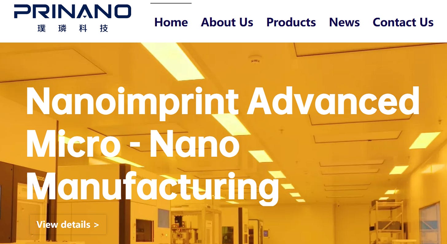
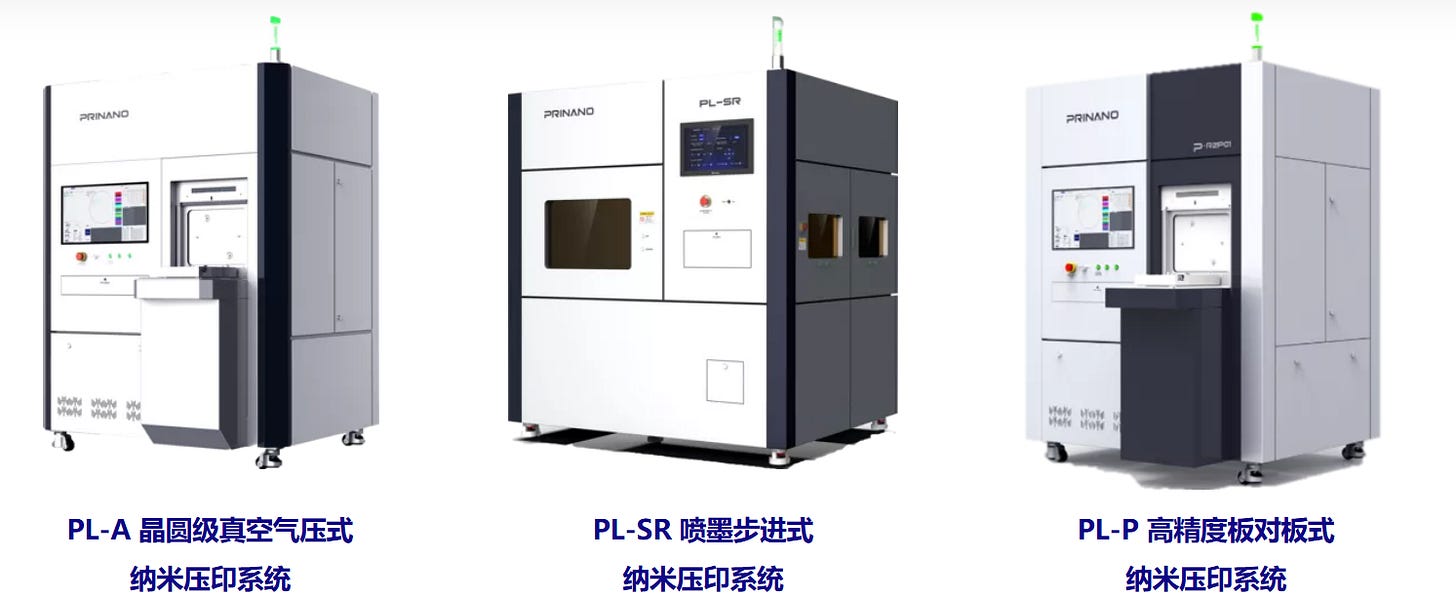
In the NIL (Nanoimprint Lithography) field,EVG, Canon, and SUSSeach have distinct focuses:
EVGtargetshigh-volume optical manufacturingfor AR/MR waveguides, meta-optics, and related applications.
Canonfocuses onsemiconductor production lines, leveraging its lithography expertise for wafer-level NIL.
SUSSprovides aflexible R&D platformand multi-purpose NIL solutions for optics, MEMS, and microfluidics.
Theglobal NIL supply chainis already taking shape, spanning equipment vendors, process and materials suppliers, research institutes, and emerging regional players.
However, themarket entry barrier remains high: precision, reliability, and mass-production consistency are still the critical benchmarks for NIL adoption.


PreviousNext
TopLatestDiscussions








See all