Lightmatter: Transforming AI Infrastructure with the Power of 3D Photonics
Lightmatter: Transforming AI Infrastructure with the Power of 3D Photonics
- Source: SemiVision
- Author: SEMIVISION
- Published: 2025-08-29T15:25:16+08:00
- URL: https://tspasemiconductor.substack.com/p/lightmatter-transforming-ai-infrastructure Lightmatter: Transforming AI Infrastructure with the Power of 3D Photonics


Lightmatter: Transforming AI Infrastructure with the Power of 3D Photonics
Original Articles By SemiVision Research (Hotchip . Nvidia , Broadcom , Marvell , Lightmatter , Celestial AI , AyarLab ,Lightelligence)

Aug 29, 2025
∙ Paid

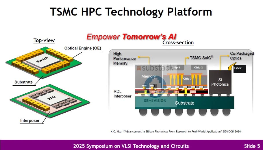
TheHot Chips conferenceis about to begin, marking a pivotal moment in the evolution of AI infrastructure. As large-scale models continue to expand, the bottleneck in performance is shifting—away from the raw compute of individual processors and toward theinterconnects and data movementthat bind entire systems together. Traditional electrical interconnects are increasingly constrained in efficiency, latency, and scalability, struggling to keep pace with the demands of generative AI and ultra-large-scale training workloads.


2025年6月22日
Against this backdrop, the introduction ofphotonicsis emerging as a core force driving the next generation of AI computing architectures. In particular,3D photonic interconnectspromise not only higher bandwidth density and lower power consumption, but also the ability tofundamentally redefine how processors and datacenters are linked at the architectural level.

Today, our attention turns to the latest advances fromLightmatter, a pioneer in photonic computing and photonic interconnects. At this year’s Hot Chips, the company will deliver a keynote presentation:
“Transforming AI Infrastructure with the Power of 3D Photonics.”
This topic extends far beyond a single technological breakthrough—it is intimately tied to the future of the entire AI ecosystem. How can datacenters operate with the efficiency of a unified supercomputer? How can compute performance continue to scale even as power consumption rises relentlessly?3D photonic interconnects may hold one of the most promising answers.
Nick Harris
Founder and CEO of Lightmatter

Title:Transforming AI Infrastructure with the Power of 3D Photonics
Abstract:
3D photonics’ edgeless I/O paradigm overcomes the reach and bandwidth limits of traditional interconnects, linking thousands of GPUs with unprecedented scale-up throughput and energy efficiency. This talk will unpack the enabling technologies—silicon photonics integration, 3D packaging and high-density laser arrays—that make faster, more efficient AI model training and next-generation data-center architectures possible.
Biography:
Nick Harris is the founder and CEO of Lightmatter, a pioneering photonic-computing company that is redefining AI infrastructure. An MIT-trained engineer and scientist, he won the MIT Technology Review’s TR35 award and holds numerous patents on revolutionary photonic technologies. His prolific research—published in top-tier journals such as Nature—has seeded new fields in photonic AI interconnects, processor design, and quantum computing. Under his leadership, Lightmatter has introduced the world’s fastest AI interconnects and set the industry benchmark for energy-efficient, high-performance 3D photonics, shaping the future of computing.
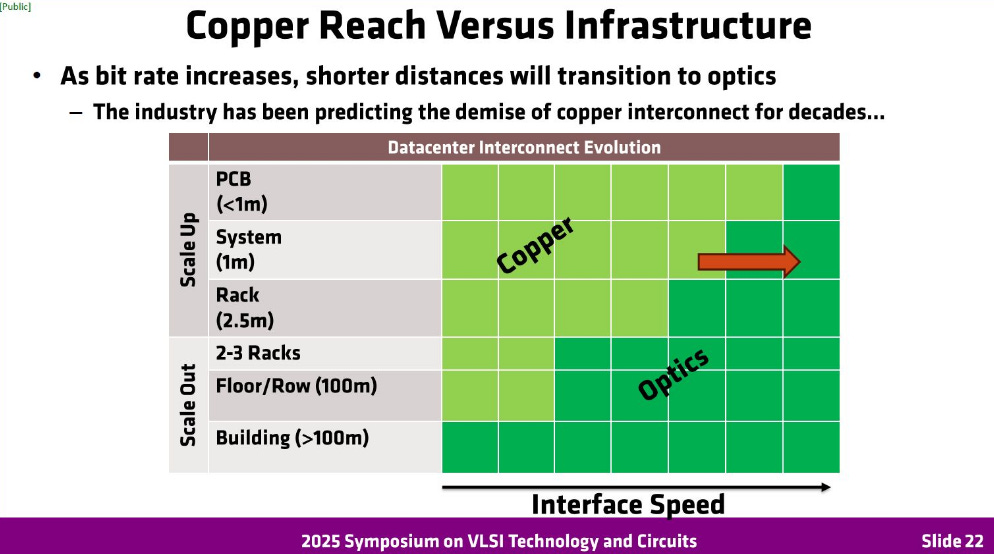
Copper remains viable for sub-meter and system-level connections, but optics is becoming essential for rack-scale and beyond.
In the rapid evolution of AI infrastructure,optical interconnectionhas emerged as a core technology to overcome the limitations of traditional electrical interconnects. As large-scale models demand ever-higher bandwidth, lower latency, and greater energy efficiency, a new wave of startups and pioneering companies focused on photonics is rising—driving efforts to reshape the network architectures of data centers and high-performance computing.
Among them,Lightmatterleads the industry with itsPassage 3D photonic interconnect platform, featuring high-density DWDM transmission and co-packaged optics (CPO) solutions.Celestial AI, on the other hand, leverages itsPhotonic Fabrictechnology to decouple memory from compute, enhancing the scalability of AI clusters.Ayar Labsfocuses onphotonic I/Oto replace traditional SerDes, delivering more efficient interconnects between servers and GPUs. Meanwhile,Lightelligencecombines photonic computing with interconnect technologies in an attempt to build an end-to-end optoelectronic acceleration platform.


2025年7月4日
Together, these companies form thecore camp of photonic interconnect innovators. They are not only pushing forward the technologies that will power the next generation of AI computing, but also demonstrating diverse pathways through which data centers may transitionfrom electricity to light.
The introduction of photonic interconnects not only alleviates the bandwidth bottlenecks between GPUs, CPUs, and specialized accelerators, but also triggers a complete reconfiguration ofadvanced packaging, memory architecture, network protocols, and data center topology. From on-chip photonic I/O to optical switching across racks and even entire facilities, the AI compute chain is rapidly converging toward a design paradigmcentered on light.
This also means that future competition will no longer be defined by hardware specifications alone, but by who can first establish aholistic photonic platform that integrates hardware, software, and ecosystem support. Lightmatter is advancing this vision with its dual-engine strategy of Passage (interconnect) and Envise (compute); Celestial AI targets memory disaggregation through its Photonic Fabric; Ayar Labs and Lightelligence pursue I/O and photonic acceleration respectively. While each company follows a different path, they all point toward the same trend—the transition of data centers from electrical to photonic architectures.
On the stage of Hot Chips, these forward-looking concepts represent more than technical showcases; they signal the direction of the entire industry. For those tracking the future of AI, this “photonics revolution” is not only about faster GPU links or larger model scales—it is ultimately about whether AI can continue to expand under the dual constraints ofenergy and cost.
For Paid Members, SemiVision will discuss topics on
Lightmatter
Celestial AI
Ayar Labs
Lightelligence
Lightmatter: Using Photonic Computing to Address the AI Energy Crisis
The Story of Lightmatter: A Photonic Journey from MIT Labs to the Future of AI
Spotlight on Lightmatter: The Three Core Products—Passage, Envise, and Idiom
Passage: The Optical Interconnect Platform
Envise: The Photonic AI Accelerator
Idiom: The Photonic Computing Software Platform
Lightmatter’s Dual-Engine Strategy
Lightmatter : Market Landscape
-
Data Centers — Reducing Energy, Enhancing Scalability
-
AI Technology Companies — Tackling Compute Bottlenecks in Vertical Domains
-
Cloud Service Providers — Breaking Traditional Networking Bottlenecks
Competitive Landscape: NVIDIA, Broadcom, Marvell vs. Lightmatter
Lightmatter’s Differentiation
Market Size in Global AI Product and Service Market
AI Market Outlook & Lightmatter’s Challenges
Competitors in Photonic Compute & Interconnect (Celestial AI / Ayar Labs )
Competition from Traditional Semiconductor Giants (NVIDIA / Cerebras Systems )
Lightmatter’s Position
Business Model in Lightmatter
Strategic Outlook
Quantum and Photonics Funding Boom
Key Opportunities
Key Risks
Lightmatter’s Core Opportunities vs. Challenges
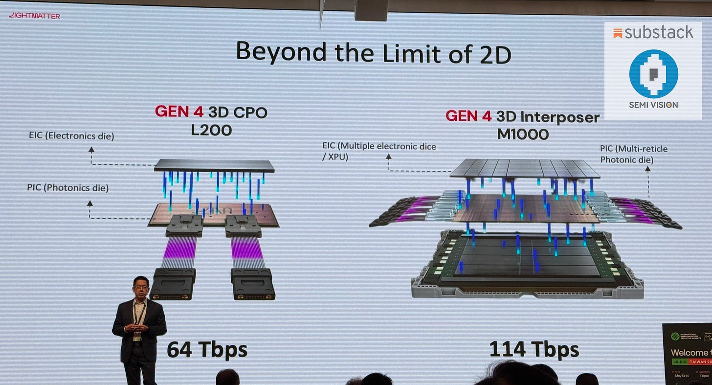
Silicon Photonics Integration: PIC and EIC Synergy
Architectural Impact: Radix Expansion & Topology Optimization
Lightmatter
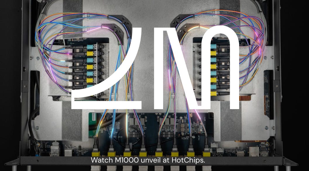
Lightmatter’s core strength lies in itsPassage 3D photonic interconnect platform, which integratesDWDM (Dense Wavelength Division Multiplexing)withCo-Packaged Optics (CPO)within a single package. This design enables up to16 wavelengths on a single fiber, delivering extremely high bandwidth density and low-power data transmission. It is particularly suited for the massive interconnect demands ofAI clusters and wafer-scale computing. Lightmatter positions itself as acomprehensive photonic interconnect solutions provider, extending its roadmap beyond interconnects intophotonic computing chips (Envise)—giving it a first-mover advantage in the convergence of optics and compute.
Celestial AI
Celestial AI focuses on its Photonic Fabric architecture, which emphasizes compute-to-memory disaggregation. Its platform establishes ultra-high-bandwidth, low-latency optical links between processors and memory, directly addressing the “Memory Wall” problem in large-scale AI training. By enabling efficient memory access for models with massive parameter counts, Celestial AI is positioned as a leader in memory interconnect and data-access optimization, making it particularly valuable for workloads requiring both high throughput and scalable memory bandwidth.

Ayar Labs

Lightelligence
Lightelligence takes a different path, combiningphotonic computingwithphotonic interconnectsto build anend-to-end optoelectronic acceleration platform. Beyond developingphotonic AI accelerators(e.g., the PTC series), the company has expanded into interconnect technologies, aiming to integrate compute cores and interconnect layers into a unified architecture.
Its product portfolio includes:
PACE– A photonic compute engine optimized for matrix operations and specialized AI/optimization workloads.
Hummingbird (oNOC)– An on-chip optical network (optical Network-on-Chip), designed with anall-to-all broadcast topologyto improve latency and energy efficiency.
Photowave™– A data center–level photonic interconnect platform, compatible withPCIe/CXL protocols, enabling higher-efficiency inter-server and inter-rack connections.
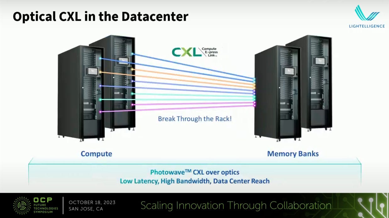

With this full-stack strategy, Lightelligence is not just competing against NVIDIA in the compute domain but is also entering the interconnect race, offering a“photonic system-level solution.”Unlike peers who specialize in a single domain (e.g., Ayar Labs on Optical I/O, Celestial AI on memory interconnect), Lightelligence differentiates itself as across-domain playerwith a more ambitious vision: to deliver a complete photonic ecosystem that spans from chip-level compute to data center–scale interconnect.

Short summary:
Lightmatter =broad platform player, bridging compute + interconnect.
Celestial AI =memory interconnect specialist.
Lightelligence =ambitious full-stack contender, integrating compute + interconnect for a holistic solution.
Lightmatter: Using Photonic Computing to Address the AI Energy Crisis
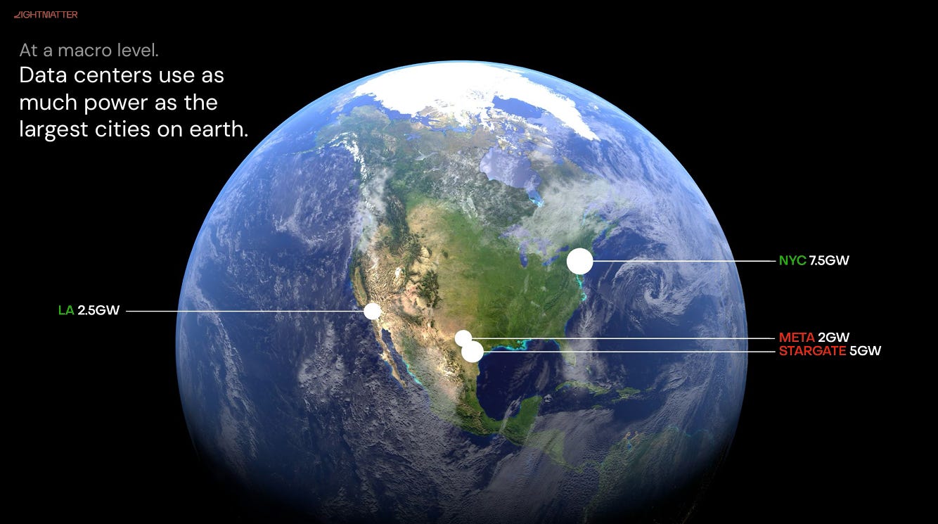
The world’s data centers are consuming energy at an astonishing pace. Forecasts suggest that by2026, their electricity usage willdouble, reaching a level equivalent to Japan’s annual power consumption. More strikingly, as ofOctober 2024, data centers dedicated to artificial intelligence (AI) already account for70% of incremental energy demand.The surge comes from two fronts: the immense power required to train foundation models and the ongoing consumption generated by inference workloads from services like ChatGPT, Claude, and other generative AI platforms.

Take ChatGPT as an example. ByAugust 2024, the platform had over200 million weekly active users, consuming roughly564,000 kWh of electricity per day. Just six months later, its user base doubled to 400 million, suggesting that energy demand may have doubled as well. Even Deepseek—celebrated for its efficient R1 model—consumes power levels comparable to, if not higher than, rival AI systems.

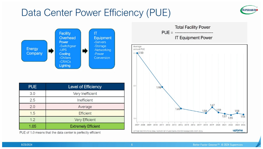
Energy consumption is not only about computation.Coolingis a parallel drain. AI processors generate enormous heat, overwhelming traditional air-cooling systems, which require constant energy input to maintain stable temperatures. Liquid cooling is therefore emerging as a critical solution. As of August 2024,22% of data centershad adopted liquid cooling; by 2029, that figure is expected to rise to50%.

Against this backdrop,Lightmatterpositions itself as a disruptor, usingphotonic computing and photonic interconnectsto attack the energy bottleneck head-on. By processing and transmitting data with light rather than electrons, Lightmatter aims to deliver higher computational throughput while cutting energy use—precisely where AI workloads and data-intensive applications are most constrained.
Nicholas Harris, Lightmatter’s CEO, has been explicit about this vision:
“Within the next few years, every GPU used for AI training and inference will be built on the Passage platform.”
ThePassage platform, Lightmatter’s flagship 3D photonic interconnect, is designed to scale data centers beyond the limits of electrical interconnects. By combiningDWDM (dense wavelength division multiplexing)andco-packaged optics (CPO), Passage enables ultra-high bandwidth density at lower power, directly tackling the energy overhead of traditional architectures.
In essence, Lightmatter is not just developing another chip; it is proposing a paradigm shift. If successful, its technology could enable AI infrastructure to keep expanding without overwhelming global power grids—anew path for the sustainability of the AI revolution.

The Story of Lightmatter: A Photonic Journey from MIT Labs to the Future of AI


Source: CNBC
The Founding of Lightmatter (2017)
Lightmatter was founded inSeptember 2017by three co-founders whose diverse expertise brought together the worlds ofsemiconductors, photonics, quantum science, and business strategy.
Nicholas Harris (CEO)brought the vision. Before founding Lightmatter, he worked as an R&D engineer atMicron Technology, focusing on DRAM and NAND circuit design. During his PhD and postdoctoral research atMIT, Harris concentrated on quantum and photonic computing. His doctoral thesis,“Programmable Nanophotonics for Quantum Information Processing and Artificial Intelligence,”outlined how nanophotonic architectures could overcome the bottlenecks of traditional computing. At MIT, he led the Quantum Photonics Laboratory, published69 research papers, and secured17 patents—credentials that positioned him at the forefront of photonics-driven computing innovation.
Darius Bunandar (Chief Scientist)complemented Harris on the scientific front. Bunandar earned dual undergraduate degrees inPhysics and Mechanical Engineeringat the University of Texas at Austin, before completing aPhD in Physics at MIT in 2018. His expertise in photonics and quantum computing was integral to transforming Harris’s conceptual frameworks into viable technological pathways.
Thomas Graham (CFO, former COO)provided the operational backbone. With a background in finance and corporate strategy, Graham worked atMorgan StanleyandGooglebefore earning his MBA from theMIT Sloan School of Managementin 2018. His experience in scaling organizations and securing capital would prove critical in transitioning Lightmatter from a research idea into a business.
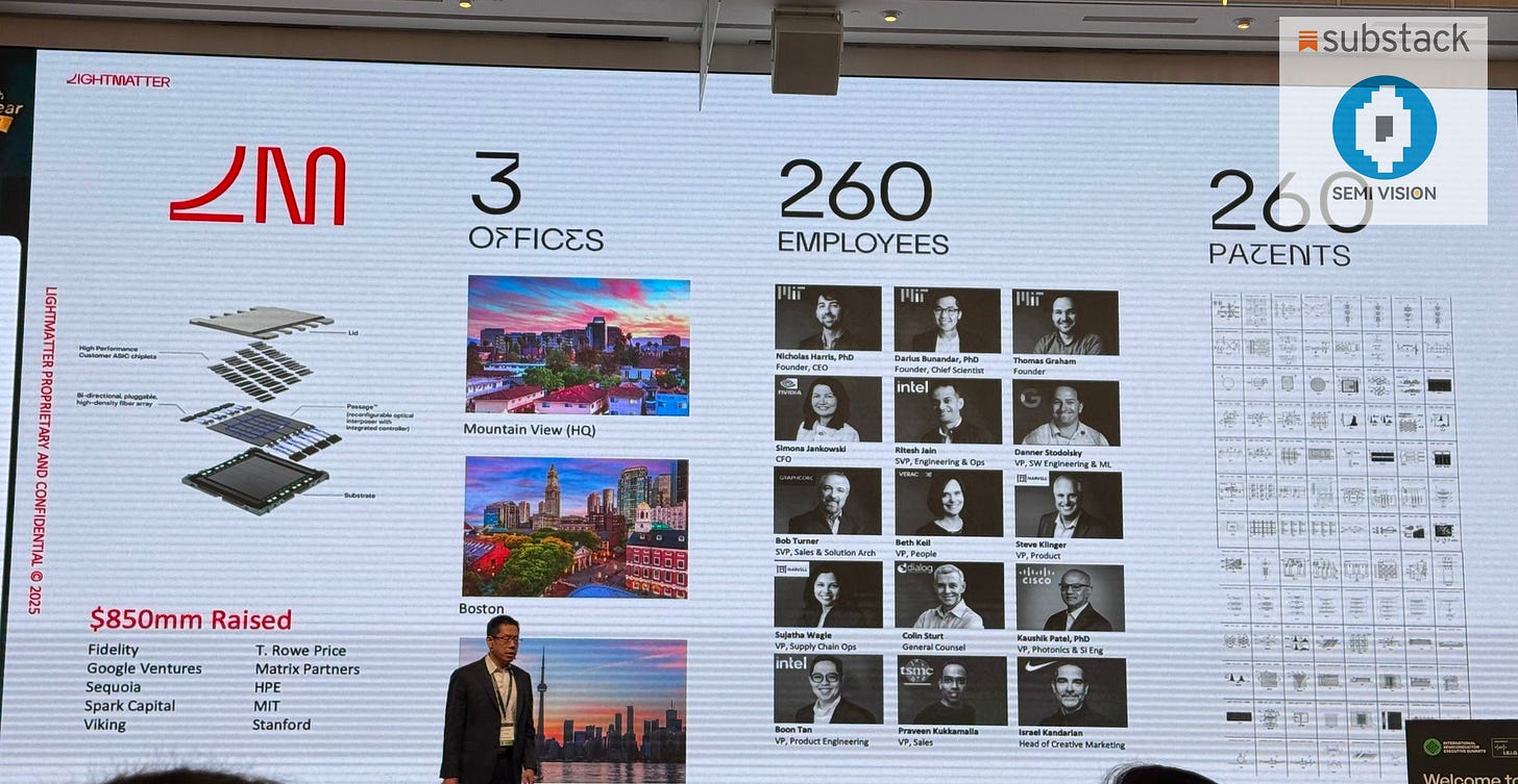
The three co-founders first crossed paths on theMIT campus. Harris and Bunandar were immersed in photonics experiments at MIT’s quantum lab, while Graham was pursuing management studies at Sloan. Harris realized that the photonic systems originally developed for quantum computing could also revolutionizedeep learning, where compute and energy bottlenecks were becoming unsustainable. This insight changed the trajectory of his career. Instead of becoming a professor, Harris decided to build a company. Together with Bunandar and Graham, he launchedLightmatter.
In its first year, Lightmatter entered MIT’s startup competition and won$100,000 in seed funding—a milestone that allowed the team to formally embark on their journey. What began as an academic experiment soon evolved into a startup with the ambition toredefine the future of AI infrastructure through photonics.
Management Evolution
Since its founding in 2017,Lightmatter’s leadership teamhas gone through several notable transitions, reflecting the company’s shift from an MIT spin-out to a scaling deep-tech enterprise.
Thomas Graham, one of the three co-founders, initially served asCOO from 2017 to May 2023. During this period, he was instrumental in shaping Lightmatter’s early operations, fundraising strategy, and company culture. In mid-2023, Graham transitioned into the role ofCFO, focusing more directly on financial structuring and investor relations while maintaining his role as a co-founder within the leadership circle.
InJuly 2024, Lightmatter appointedSimona Jankowskias its newCFO. Jankowski brought with her an impressive background as aformer Managing Director at Goldman Sachsand later asVice President of Investor Relations and Strategic Finance at NVIDIA. Her appointment was widely seen as a strategic move, signaling Lightmatter’s ambition to position itself not just as a technology pioneer, but also as a company capable of navigating Wall Street, global capital markets, and the investor expectations that come with scaling transformative infrastructure.
As ofFebruary 2025, Graham continues to remain at Lightmatter in his capacity as aco-founder, still engaged with the company’s internal operations and long-term vision. This continuity provides stability while Jankowski steers the financial strategy toward Lightmatter’s next stage of growth.
These leadership transitions have occurred against a backdrop ofescalating global energy pressures in data centers. AI workloads, particularly the training and inference of large-scale models, are driving unprecedented demand for power and interconnect efficiency. Lightmatter’s combined platform ofphotonic computing and its Passage photonic interconnect systemdirectly addresses these challenges, offering a path to reduce energy consumption while increasing scalability.
FromNicholas Harris’s foundational research at MITon programmable nanophotonics to Lightmatter’s emergence as an industry reference point, the company’s trajectory has mirrored one of the most urgent questions facing the semiconductor and AI ecosystem:how can the expansion of AI be sustained under finite energy constraints?
Looking ahead, the next several years will be decisive. As data center scale and AI power consumption continue to grow, Lightmatter’s ability tomove Passage into mass production and broad adoptionwill determine whether it can establish itself as acore infrastructure provider in the photonic computing era. If successful, Lightmatter won’t just be a startup story—it will be a cornerstone of how the world powers the next generation of artificial intelligence.
Company Products
Background: Moore’s Law and the Energy-Efficiency Bottleneck
For decades, advances in computing power have been driven by two fundamental forces:
Moore’s Law: Transistor density doubling approximately every two years, driving exponential growth in processor performance.
Dennard Scaling: As transistors shrank, power density remained constant, enabling improved energy efficiency as chips became smaller.
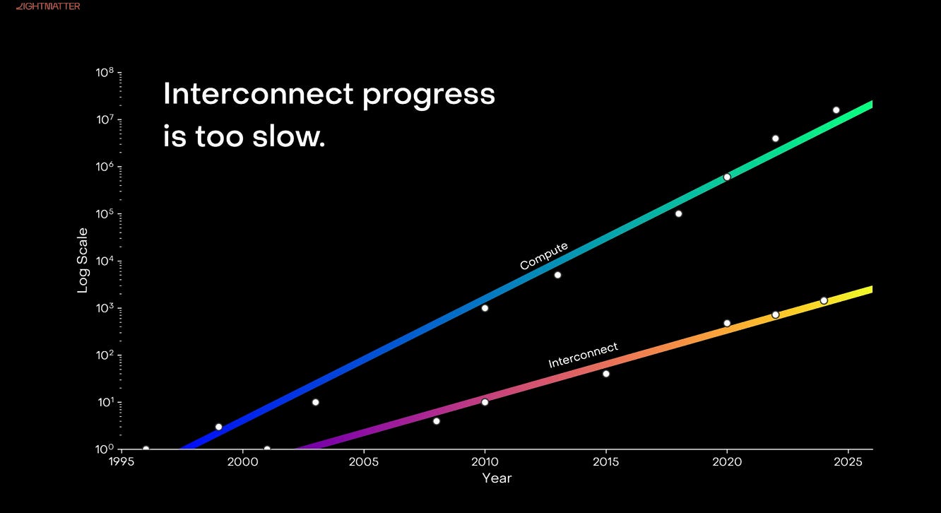
These trends underpinned decades of exponential performance improvements and cost reductions across the information technology industry. However, since around2005, transistor scaling has been approaching physical limits. Gains in energy efficiency and cost improvements have slowed dramatically. This means that relying solely on traditional semiconductor process advances is no longer sufficient to meet the rising compute demands of AI and high-performance computing (HPC).
Nicholas Harris,Lightmatter’s CEO and founder, recognized this limitation and proposedphotonic computingas a breakthrough path forward:
“Photonics allows computation to occur in parallel, because different colors of light can each carry separate streams of data simultaneously. For example, red light can transmit an image of a dog, green light an image of a cat, and blue light an image of a tree. All of this information can be processed at the same time within a single photonic matrix accelerator, enabling much higher compute density and energy efficiency per unit area.”

Spotlight on Lightmatter: The Three Core Products—Passage, Envise, and Idiom
Building on this vision, Lightmatter has introduced three flagship products:
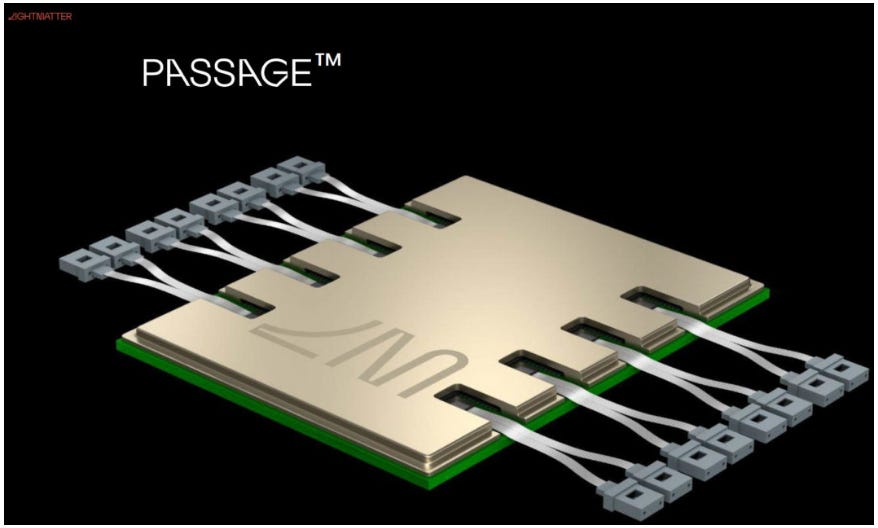
Passage– aphotonic interconnect chipdesigned to overcome data center bandwidth bottlenecks.
Envise– aphotonic computing acceleratorbuilt to directly handle AI workloads.

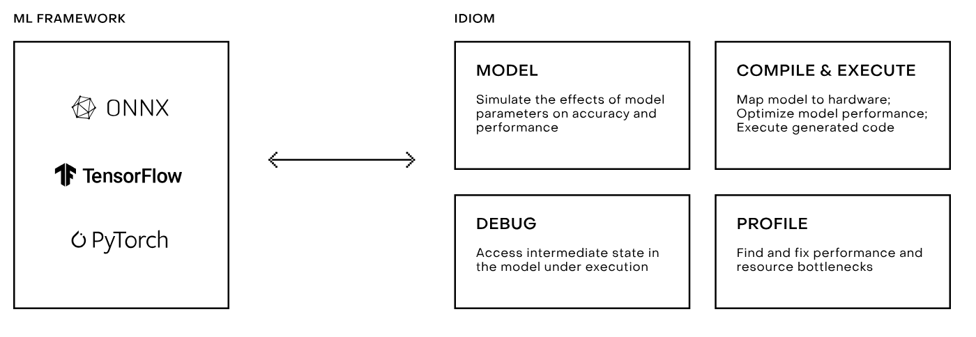
Idiom– asoftware toolchainthat improves the usability and efficiency of photonic computing platforms.
Passage: The Optical Interconnect Platform
Positioning
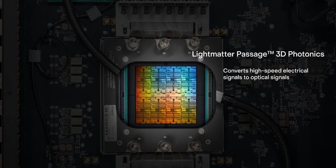
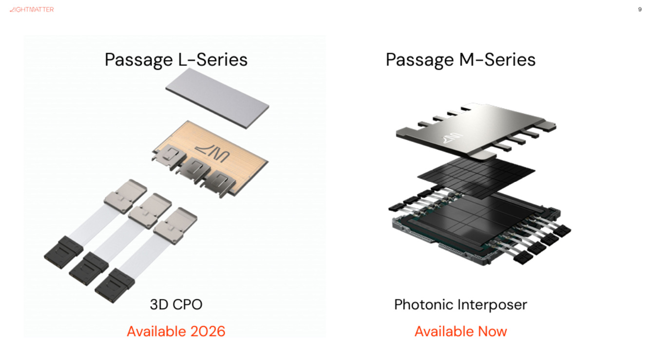
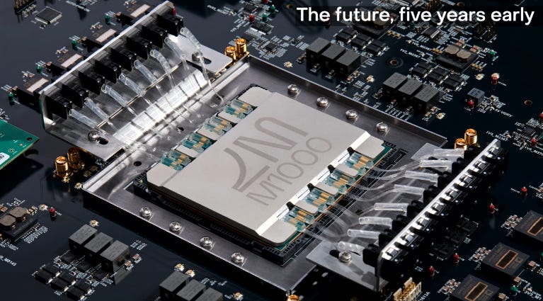
Passage isLightmatter’s photonic interconnect platform, designed to tackle one of the most pressing challenges in modern AI infrastructure:high-speed data transfer between GPUs, CPUs, and XPUs inside data centers. Unlike traditional PCB-based electrical interconnects, Passage embedssilicon photonics directly into the packaging layer, enabling chip-level optical communication. This approach directly addresses today’s biggest bottlenecks in AI clusters—I/O bandwidth limitations and insufficient port density.
Architecture and Operating Principle
At its core, Passage functions as aphotonic interposer:
It can sit between processors and memory (such as SRAM), allowing data to traveloptically within the package.
Usingoptical I/O, it supports bothchip-to-chipandnode-to-nodecommunication.
ThroughDense Wavelength Division Multiplexing (DWDM),multiple wavelengths can travel simultaneously on a single fiber, dramatically boosting bandwidth density.
Key Features
Compatibility with existing hardware: Seamlessly integrates with today’s GPUs and CPUs, without requiring a full overhaul of existing infrastructure.
Ultra-high bandwidth: Provides100 Tbps-class optical bandwidth, far exceeding current electrical SerDes interconnects.
High-density packaging: Can connect up to48 processors(GPUs, CPUs, or photonic accelerators) in a single interconnect network.
Photonic channel design: Up to40 optical channels compressed into a single fiber, reducing routing complexity and space requirements.
Value Proposition
Infrastructure efficiency: Significantly reduces the number of fibers and switch ports needed in data centers, alleviating space and cabling constraints.
Scalability: Enables larger and more efficient AI training and inference clusters.
Energy savings and signal integrity: Compared to PCB-based signal routing, Passage offers lower power consumption, higher signal fidelity, and better thermal stability.
Broader Significance
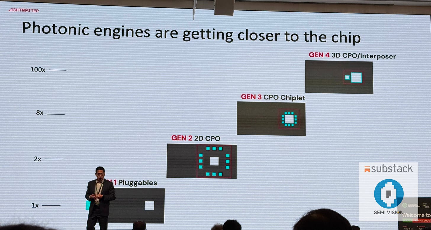
Passage represents a decisive step away from the constraints of copper wiring and PCB routing, paving the way forphotonics-centered co-packaged optics (CPO) architecturesin next-generation data centers. By embedding photonics directly into the compute fabric, Lightmatter provides a scalable solution to supportever-growing AI modelswithout overwhelming power budgets or interconnect complexity.
In essence, Passage is not just an interconnect—it is anenabling platformthat could redefine the architecture of high-performance computing and accelerate the transition towardall-optical AI infrastructure.
Envise: The Photonic AI Accelerator

Positioning
Envise is the world’sfirst general-purpose photonic AI accelerator, a groundbreaking processor that integrateselectronic computing (EIC)andphotonic computing (PIC)within a single platform. Unlike conventional interconnect products, Envise is designed to directly execute neural network tasks, making it not just a communication layer but afull-fledged photonic processorfor AI workloads.
Architecture and Design
Optical Matrix Accelerator: Harnesses optical interference and wavelength-division multiplexing (WDM) to acceleratematrix multiplications—the foundational operation of neural networks.
Electro-Photonic Co-Design: EIC handles control, logic, and device driving; PIC delivers ultra-fast computation and transmission. Both are tightly integrated throughadvanced packagingfor seamless cooperation.
Scalable Interconnect: Each chip supports6.4 Tbps optical interconnect, allowing Envise to scale from a single device tomulti-server clusterswith minimal bottlenecks.
Performance and Energy Efficiency
Power Consumption: A blade server built with16 Envise chips consumes only 3 kW, compared to 6.5 kW for an equivalent NVIDIA A100 system—representing a54% improvement in energy efficiency.
Memory Configuration: Each Envise chip supports1 TB of DDR4 DRAMand3 TB of SSD storage, enabling the handling of large-scaleLLMs (Large Language Models)and diverse AI workloads.
Software Ecosystem: Envise isnatively compatible with PyTorch, allowing developers to deploy neural networks without modifying their codebase, ensuring seamless adoption.
Application Scenarios
Envise is designed for a wide spectrum of AI workloads, including:
Conversational AI and voice assistants
Autonomous driving systems
Generative AI platforms(e.g., ChatGPT, Claude)
Large language models (LLMs)and other deep learning applications
By combining high throughput, low latency, and superior power efficiency, Envise emerges as aheterogeneous AI compute platform—one that complements and extends beyond traditional GPUs, addressing their core limitations inenergy consumptionandmemory bandwidth.
Extended Outlook
Envise represents more than an incremental performance boost—it signals aparadigm shiftin how AI workloads can be accelerated. By moving from electron-based to photon-based computation, Envise demonstrates that AI models no longer need to be constrained by Moore’s Law or the thermal ceilings of silicon. In a world where AI energy demand is skyrocketing, Envise offers a path towardsustainable scaling of intelligence infrastructure.
If successfully scaled into production, Envise could become a cornerstone technology for future data centers—bridging the gap betweenAI’s growing computational appetiteand theplanet’s finite energy resources.
Idiom: The Photonic Computing Software Platform
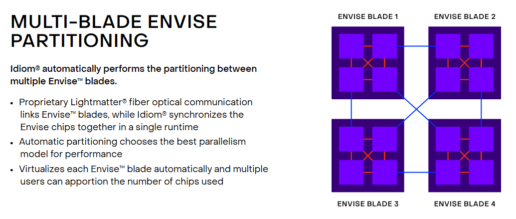
Hardware alone cannot unlock its full potential without the right software ecosystem. Recognizing this, Lightmatter builtIdiom, a complete software platform designed specifically forEnvise, ensuring that neural networks can run efficiently in a photonic computing environment. Idiom bridges the gap between novel photonic hardware and the workflows familiar to AI developers, making next-generation acceleration both accessible and practical.
Core Modules
idCompile (Graph Compiler)
Automatically partitions large neural networks into smaller, parallelizable modules and distributes them across multiple Envise units.
Supportsdata parallelismandmixed-precision computing, striking a balance between accuracy and energy efficiency.
idProfiler (Performance Analyzer)
Provides real-time monitoring of memory usage and compute unit efficiency.
Assists developers in identifying system bottlenecks and optimizing workload allocation strategies.
idBug (Parallel Debugging Tool)
Purpose-built for multi-chip parallel environments.
Enables fast error detection and correction across distributed workloads.
idML (Machine Learning Optimization Toolkit)
Deeply integrated withPyTorch, offering model quantization and knowledge distillation features.
Providesquantization-aware training (QAT), parameter visualization, and advanced model optimization, reducing computational costs while improving efficiency.
Value Proposition
Idiom’s role is totransform photonic computing from a laboratory concept into production-grade AI infrastructure.By enabling seamless deployment of Envise, it lowers barriers for developers while maximizing performance under strict energy constraints. With Idiom, developers can harness the advantages of photonics—massive parallelism, high bandwidth, and low power—without rewriting their models or abandoning existing machine learning ecosystems.
Extended Perspective
The importance of Idiom goes beyond enabling a single chip—it is thesoftware fabricthat will determine whether photonic computing scales across industries. Just as CUDA unlocked the GPU revolution, Idiom could become the defining software layer forphotonic acceleration, shaping how AI engineers build and deploy models in the coming decade. By providing a familiar programming interface and robust optimization tools, Idiom positions Lightmatter not only as a hardware innovator but also as aplatform company, cultivating an ecosystem that extends photonics into mainstream AI development.
In this sense, Idiom is not just a companion to Envise—it is thekey enablerthat allows photonic hardware to transition from experimental prototypes intoreal-world AI infrastructure.
Lightmatter’s Dual-Engine Strategy
Lightmatter’s product roadmap reveals a deliberatedual-engine strategy:
Passage→ Solves the“bandwidth and energy bottleneck”inside data centers.
Envise→ Directly challenges traditional GPUs, offeringenergy-efficient AI compute capability.
Idiom→ Serves as thesoftware ecosystem glue, lowering barriers for development and deployment.
Together, these three components form acomplete photonic computing ecosystem. In the post-Moore’s Law era—where both Moore’s Law and Dennard scaling have broken down—Lightmatter is not simply chasing incremental performance gains. Instead, it is attempting tore-architect the entire stack of compute, interconnect, and software.
IfPassageandEnviseachieve broad deployment across hyperscaler data centers, Lightmatter has the potential to emerge as acore infrastructure provider of the photonic AI era, mirroring the role that NVIDIA’sCUDA ecosystemhas played in the GPU-driven AI boom.

Lightmatter : Market Landscape
Customer Segments
As demand for AI foundation models and high-performance computing (HPC) surges, the need forefficient, energy-saving, and scalable data processing solutionshas reached unprecedented levels. Lightmatter’sPassage photonic interconnect platformandEnvise photonic acceleratorare designed to address these demands, with a focus on three core customer groups:
- Data Centers — Reducing Energy, Enhancing Scalability
Global data centers face dual pressures:doubling energy consumptionandexploding cabling complexity.Traditional electrical interconnect architectures require massive copper cabling and switch stacking, which becomes unsustainable when AI clusters scale to hundreds of thousands of GPU nodes. Operators often face what engineers call the“giant spaghetti of cables”problem.
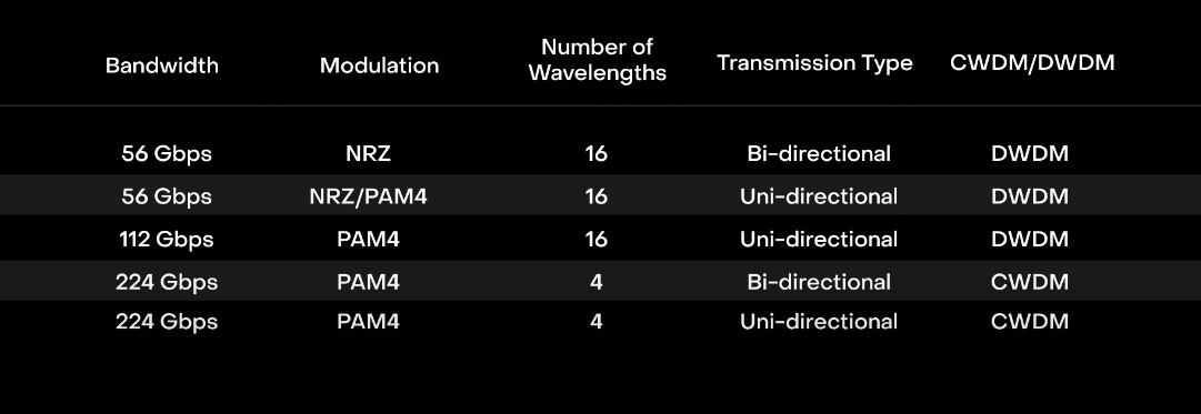
Passage solves this withDWDM technologyandco-packaged optics (CPO), transmitting multiple wavelengths of data through a single fiber. This dramatically reduces fiber and switch requirements while offering higher radix (I/O port scalability). Lightmatter can even customizesilicon photonic interconnect solutionsto match customers’ server floorplans, optimizing data paths.
As early as 2020, Lightmatter entered discussions withAmazon (AWS)andGoogle, showcasing Passage as an alternative to PCB wiring. This demonstrates its early penetration into the procurement and testing pipelines ofhyperscale operators.
- AI Technology Companies — Tackling Compute Bottlenecks in Vertical Domains
Companies building AI for specialized fields (e.g., healthcare, finance, insurance) face growing computational needs. For example,DeepScribeandFreedprocess large-scale medical speech and clinical data, requiring vast compute for transcription and decision support.
For such companies, algorithmic optimization and incremental GPU scaling are no longer enough—the bottleneck has shifted to theinterconnect layer.Stable, low-latency communication between compute components determines whether these workloads run efficiently.
Lightmatter’sEnvise + Passagecombo offershigher efficiency and lower latency interconnects, reducing reliance on endless GPU expansion. For industries handlingreal-time sensitive data—such as healthcare or financial services—this solution is especially critical.
- Cloud Service Providers — Breaking Traditional Networking Bottlenecks
With the commercialization ofGenerative AIandLarge Language Models (LLMs), cloud giants (AWS, Google Cloud, Microsoft Azure) must deliver enormous compute capacity to serve hundreds of millions of users. But currentEthernet/InfiniBand architectureshave reached their bandwidth and latency limits.
As CEONicholas Harrisnoted:
“Cloud providers already recognize the limitations of traditional networking. More efficient, higher-bandwidth interconnect technologies have become indispensable infrastructure.”
In this context, Passage enables hyperscalers to support massive GPU/XPU clusters withfewer fibers, lower power, and simpler cooling requirements, directly improving bothCAPEX and OPEX efficiency.

Lightmatter is not just a point-solution vendor—it positions itself as a full-stack AI infrastructure provider. In an era of exponential AI energy demand, its customer pain points align precisely with the market fit of Passage and Envise
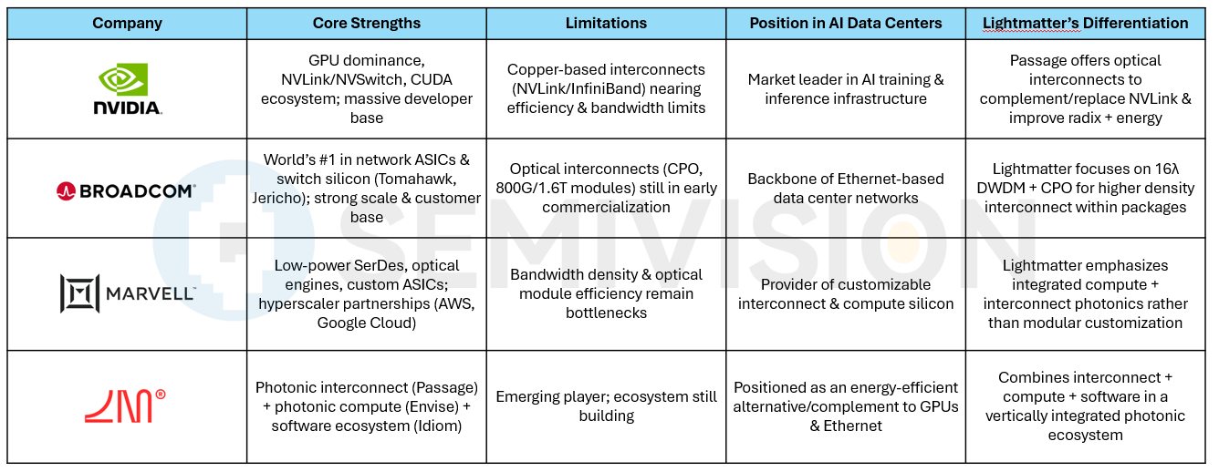
Competitive Landscape: NVIDIA, Broadcom, Marvell vs. Lightmatter
While Lightmatter is carving out its niche withphotonic interconnectsandphotonic accelerators, in the data center market it competes against established semiconductor and networking giants.
NVIDIA
Currently thedominant player in generative AI infrastructure, NVIDIA commands most of the AI training market through itsGPUs, NVLink/NVSwitch, and CUDA ecosystem. Its major customers include AWS, Google, Microsoft, and Meta. NVIDIA’s strength lies in itscomprehensive software stack and vast developer ecosystem, but its interconnects still rely on copper-based NVLink and InfiniBand, both of which are approaching limits inenergy efficiency and bandwidth density.

2025年5月28日
Broadcom
As the world’s largest supplier ofnetwork ASICs and switch silicon, Broadcom’sTomahawk and Jericho seriesare the de facto standards in Ethernet switching for data centers. Recently, Broadcom has also been pushing intoco-packaged optics (CPO)and800G/1.6T optical modulesto maintain leadership in AI data center networking. Its strength lies in itsscale and established customer base, but its optical solutions remain at an early stage of commercialization, lacking breakthroughs such assingle-fiber, 16λ BiDi multiplexingthat Lightmatter highlights.

2025年6月4日
Marvell
Marvell’s strategy is centered oncloud SerDes, optical engines, and custom ASICs, with deep collaborations with hyperscalers like AWS and Google Cloud. Its focus is onlow-power SerDesandCPO platforms, with strong emphasis oncustomizationto meet unique hyperscaler requirements. Compared with Broadcom’s standardized approach, Marvell offers greaterflexibility and differentiation, but still struggles with bandwidth density and power efficiency limits in optical modules.
2025年7月8日
Lightmatter’s Differentiation
Lightmatter’sPassageandEnvisecreate a mix of complementarity and competition:
Complementary: NVIDIA GPUs remain central to AI compute, but Passage could replace NVLink/InfiniBand, reducing power and improving radix scalability.
Differentiated: Unlike Broadcom and Marvell, which focus on Ethernet/SerDes, Lightmatter emphasizes anintegrated solution of photonic interconnect + photonic compute, bringing data transfer and computation into the same package.
Forward-Looking: Lightmatter doesn’t just provide interconnect chips—it also advances aphotonic compute roadmap (Envise)that could, in part, challenge NVIDIA’s GPU dominance.
This means Lightmatter is not attempting to replace NVIDIA, Broadcom, or Marvell outright. Instead, it is targeting thepain points they have yet to solve: bandwidth density, energy efficiency, and AI cluster scalability. If Passage and Envise achieve hyperscaler-scale adoption, Lightmatter could become acritical incremental playerin the AI infrastructure supply chain.
Market Size in Global AI Product and Service Market
Global AI Products & Services Market
According to multiple forecasts, theglobal AI products and services marketis expected to reach$780B–$990B by 2027, up from$185B in 2023, representing exponential growth.
This surge is driven by three main factors:
Commercialization of Generative AI– Applications such as ChatGPT, Claude, and Copilot are fueling both consumer and enterprise adoption.
Enterprise AI adoption– Industries such as finance, healthcare, manufacturing, and retail are accelerating AI deployments for automation and intelligent decision-making.
Expansion of cloud and edge AI– Hyperscalers offer large model training and inference services, while edge AI (IoT, autonomous vehicles) adds incremental demand.
AI Hardware Market
In2023, the AI hardware market was valued at$53.7B, and it is projected to reach$473.5B by 2033, with aCAGR of 24.5%.
Growth drivers include:
Advances in semiconductor technology(GAAFET, advanced packaging, CPO, etc.) that boost AI chip performance.
Explosion of AI inference demand– Inference, not just training, is driving massive deployments and hardware requirements.
Edge AI applications– Smart vehicles, healthcare diagnostics, and IoT are extending AI chips beyond data centers.
TheAI inference chip marketis set to be the fastest-growing segment:
Valued at$15.8B in 2023.
Expected to reach$90.6B by 2030, at aCAGR of 22.6%.
Will account for40% of the overall AI hardware market.
As inference workloads surpass training in scale, inference chip costs are expected to dominate theAI cost structure, reshaping chip design and supply chains.
Photonic Integrated Circuit (PIC) Market
Amid growing challenges of power and interconnect efficiency, thePhotonic Integrated Circuit (PIC) marketis expanding rapidly:
Valued at$8.6B in 2023.
Expected to grow to$47.6B by 2032.
CAGR:20.9%.
Key growth drivers include:
Data center energy pressure– Rising compute power drives massive electricity demand, pushing photonic computing and interconnect adoption.
AI/HPC and photonic convergence– Hyperscalers seek lower power and higher radix, fueling development of silicon photonics platforms (CPO, OIO).
5G/6G and optical communications– Beyond AI, telecom and test/measurement also expand PIC demand.
Market Positioning & Challenges
Lightmatter stands as apioneering playerin photonic computing with itsPassage photonic interconnectandEnvise photonic accelerator.However, the technology is still in itsearly commercialization phase.
Current markets remain dominated byGPU giants (NVIDIA, AMD)due to:
Ecosystem lock-in– NVIDIA’s CUDA stack and developer community.
Mature process and supply chain– Established GPU/CPU design, yield, and supply advantages.
Adoption inertia– Enterprises deeply invested in GPU infrastructure are reluctant to switch in the short term.
Thus, the success of photonic computing depends on three critical factors:
Integration with existing GPU/CPU architectures– Photonics must serve as a complementary interconnect/accelerator, not demand a full ecosystem replacement.
Standardization– Common interfaces and design toolchains must reduce development and deployment costs.
Hyperscaler adoption– Large-scale commercialization will only happen if AWS, Google, and Microsoft drive the transition.
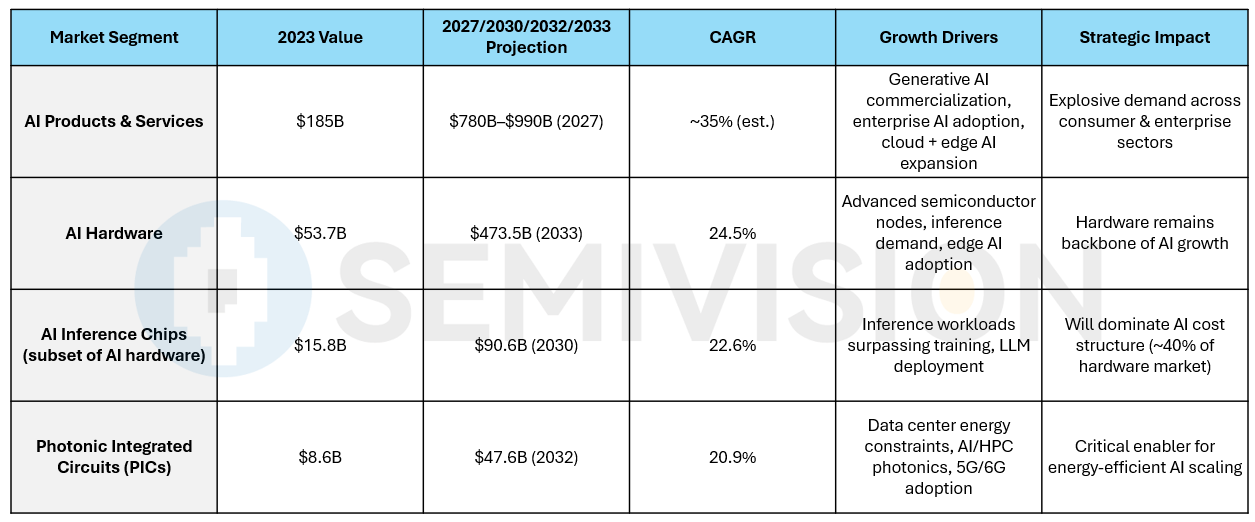
The AI market is entering exponential growth, with inference and photonic integration as the fastest-growing segments. Lightmatter’s opportunity lies at the intersection of these trends—addressing the dual bottlenecks of energy and bandwidth in the post-Moore’s Law era.
AI Market Outlook & Lightmatter’s Challenges
AI Overall Market: From 2023 to 2027, CAGR exceeds40%, driven by full-scale commercialization.
AI Hardware Market: By 2033, expected to approach$500B, withinference chipsas the growth engine.
PIC (Photonic Integrated Circuits) Market: Nearly5x growth in a decade, fueled by AI, HPC, and data center efficiency demands.
Lightmatter’s Challenge: Technologically ahead, but must overcome three barriers—integration, standardization, and customer adoption—to stand shoulder-to-shoulder with NVIDIA and AMD, and truly unlock market potential.

Global AI Products and Services Market
According to industry research forecasts, theglobal AI products and services marketis expected to reach$780B–$990B by 2027, compared to$185B in 2023, representing more than afourfold increase. This remarkable growth is driven by:
Full-scale commercialization of generative AI— Applications such as ChatGPT, Claude, and Copilot are fueling explosive growth across both enterprise and consumer markets.
Adoption in vertical industries— Finance, healthcare, retail, and manufacturing sectors are rapidly deploying AI for automation, speech recognition, and predictive analytics.
Dual growth of cloud and edge AI— Hyperscalers are expanding their AI training and inference infrastructure, while edge AI is rising in autonomous vehicles, IoT, and industrial applications.
AI Hardware Market
In2023, the globalAI hardware marketwas valued at approximately$53.7B. By2033, it is projected to grow to$473.5B, with a10-year CAGR of 24.5%.This rapid growth is fueled by three key factors:
Semiconductor breakthroughs— Advances such as next-generation process nodes, chiplet architectures, advanced packaging, and co-packaged optics (CPO) are accelerating deployment.
Rise of edge AI— Demand for low latency and real-time processing is pushing compute closer to endpoints.
Within this, theAI inference chip marketis the fastest-growing subsegment:
Valued at$15.8B in 2023.
Expected to reach$90.6B by 2030, with aCAGR of 22.6%.
Already accounts for40% of the AI hardware market.
As large models are increasingly deployed for inference,inference costs are expected to dominate the overall AI cost structure.This signals a shift in competitive focus for AI hardware—from “maximum training performance” towardinference efficiency and cost optimization.
Photonic Integrated Circuit (PIC) Market
As traditional electrical interconnects approach their efficiency limits, the value ofphotonicsis rapidly being recognized. In2023, the globalPhotonic Integrated Circuit (PIC) marketwas valued at$8.6B, and is projected to reach$47.6B by 2032, with aCAGR of 20.9%.
Key growth drivers include:
HPC and AI energy pressures— Photonic interconnects deliver significantly higher bandwidth per unit of power, making them strategically vital for data centers.
Advances in advanced packaging— Technologies such as CPO (co-packaged optics), OIO (optical I/O), and hybrid bonding are driving heterogeneous integration of photonic and electronic systems.
Emerging applications— Beyond AI training and inference, PICs are being widely adopted in5G/6G communications, quantum communication, and sensing technologies.
Market Positioning and Challenges
AlthoughLightmatteris one of the most representative startups in the field of photonic computing—pioneering with thePassage photonic interconnectand theEnvise photonic accelerator—the broader market remains in itsearly adoption phase:
NVIDIA and AMDcontinue to dominate, with matureGPU/CPU architecturesand robust software ecosystems (e.g., CUDA).
For photonic computing to gain widespread adoption, it must achieveseamless integrationwith existing hardware and software stacks; otherwise, the barriers to real-world application remain high.
Adoption and validation byhyperscalers(AWS, Google, Microsoft) will be the decisive inflection point for the commercialization of photonic computing technologies.
As such, while Lightmatter holds afirst-mover technological advantage, its market feasibility will depend on:
Compatibilitywith existing GPU architectures.
Maturity of standardization and design toolchains.
Adoption speedamong cloud hyperscalers.
At the same time, themarket opportunity is enormous:
Theglobal AI products and services marketis projected to surpass$900B by 2027, becoming a core driver of the digital economy.
TheAI hardware marketis expected to approach$500B by 2033, withAI inference chipsemerging as the key growth engine.
Thephotonic integrated circuit (PIC) marketis set to nearly5x within a decade, closely tied to energy pressures in AI and HPC.
In summary, Lightmatter sits at the technological frontier. But to truly penetrate a mainstream market dominated by NVIDIA and AMD, it must overcome the three structural challenges ofecosystem integration, standardization, and customer adoption.
Competitors
Lightmatter addresses two critical markets through its core products:
Envise (Photonic AI Accelerator):Targets high-performance AI compute, competing against traditional electronic chips.
Passage (Photonic Interconnect Platform):Focuses on photonic interconnects and co-packaged optics (CPO), challenging SerDes and copper interconnect approaches.
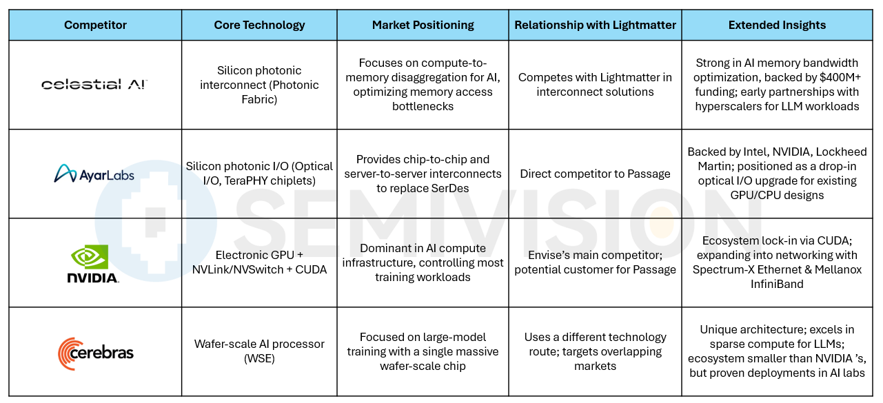
Envisedirectly competes withNVIDIA H100,Google TPU, andCerebras WSE-3, differentiating itself by replacing electronic computation withphotonics, reducing both power consumption and cooling bottlenecks.Passagecompetes withAyar LabsandCelestial AI, while networking giants likeBroadcomandMarvellcontinue to evolve along the Ethernet and SerDes roadmap.
Competitors in Photonic Compute & Interconnect
Celestial AI
Positioning:Specializes inmemory and interconnect optimization. Its flagship product,Photonic Fabric, uses silicon photonics to deliver14.4 Tbps bandwidth per linkand chiplet-based architectures to solve GPU/CPU memory access bottlenecks.
Differentiation:Like Passage, Celestial AI focuses on photonic interconnects but emphasizesmemory disaggregationand accelerator-to-accelerator communication. Lightmatter, in contrast, is building abroader photonic platformthat integrates lasers and dynamic network switching to optimize AI cluster infrastructure.
Capital Strength:As of Feb 2025, Celestial AI has raised$338.9M, backed bySamsung Catalyst Fund, Temasek, and the US Innovative Technology Fund; valuation stands at$1.2B.
Ayar Labs
Positioning:Founded in 2015, Ayar Labs focuses onOptical I/O, replacing SerDes with photonic links to improve chip-to-chip/server-to-server data transfer.
Competition:Overlaps with Passage in photonic interconnect, but emphasizespoint-to-point I/Orather than cluster-wide CPO networks.
Funding & Strategy:
May 2023: Raised$155M Series C, led by NVIDIA, to integrate Optical I/O into GPU racks.
Dec 2024: Closed another$155M Series D, surpassing$1B valuation, with investors including AMD Ventures, Intel Capital, and NVIDIA.
Total funding:$374.7M(as of Feb 2025).
Pros & Cons:Backed by major chip giants with real commercialization potential, but lacks Lightmatter’sDWDM and large-scale CPO cluster platform capabilities.
Competition from Traditional Semiconductor Giants
NVIDIA
Market Position:As of Feb 2025, market cap of$3.3T, controlling70–95% of AI chip share—an absolute market leader.
Product Strength:TheH100 GPUdominates AI acceleration, priced at ~$30,000 per unit; itsclosed CUDA ecosystemis the industry standard.
Challenges:
High costs push some customers to explore alternatives.
Single GPUs provide only80GB HBM, insufficient for trillion-parameter models, forcing massive GPU deployments that drive up costs and complexity.
Relationship with Lightmatter:
Competition:Envise directly challenges NVIDIA GPUs on efficiency and scalability.
Potential Partnership:Passage could replace or augmentNVLink/InfiniBand, offering higher bandwidth and lower power interconnects between GPUs.
Cerebras Systems
Positioning:Pursues a differentiated route withwafer-scale processors (WSE). Its latestWSE-3, deployed in CS-3 systems, is branded the “world’s fastest AI processor.”
Performance Highlights:
TrainingLLaMA 3.1 (8B and 70B)at1800 tokens/s and 450 tokens/srespectively.
Provides7,000x higher memory bandwidththan NVIDIA H100, addressing storage bottlenecks in GPU clusters.
Supports distributed compute, scaling to trillion-parameter models.
Difference from Lightmatter:
Cerebras focuses onelectronic computation + wafer-scale integration.
Lightmatter emphasizesphotonic computation + interconnectto boost efficiency and scalability.
Both disrupt NVIDIA’s GPU model, but withdifferent technological approaches.
Lightmatter’s Position
Envise: Competes head-to-head withNVIDIA GPUs, Google TPU, and Cerebras WSE, differentiating withphotonic compute efficiency and scalability.
Passage: Faces competition fromAyar Labs and Celestial AI, but offers a more advanced roadmap with16λ DWDM + CPO integration.
NVIDIA: Both a competitor and a potential customer—Passage could complement NVLink/InfiniBand.
Strategic Opportunity:If Lightmatter proves advantages inefficiency, cost, and hyperscaler adoption, it can not only challenge NVIDIA and Cerebras but also build aunique moat in both photonic compute and interconnect.

Lightmatter is unique in bridgingphotonic compute and photonic interconnect, while competitors tend to specialize in narrower domains (memory, I/O, or wafer-scale compute). This positions Lightmatter as asystem-level disruptorrather than a niche challenger.
Business Model in Lightmatter
As ofFebruary 2025, Lightmatter has not yet disclosed a specific pricing model. However, based on its product positioning and market trajectory, its business model is already beginning to take shape. The company’s core strategy is to embedphotonic interconnects (Passage)andphotonic compute (Envise)directly intoadvanced packaging and system architectures, providing data centers and hyperscale AI clusters with infrastructure solutions that are bothmore efficient and more energy-saving.
- Direct Product Sales
Lightmatter’s primary revenue stream is expected to come from thedirect sales of chips and system-level products:
Envise Photonic Accelerator:Positioned as dedicated hardware for AI/HPC training and inference. Likely to be sold in formats such assingle cards, blade servers, or complete system racks.
Passage Photonic Interconnect Platform:Can be sold as astandalone CPO interconnect moduleor as part of an integrated solution with XPUs/GPUs/CPUs/ASICs.
CEONicholas Harrishas stated that Envise’s pricing will be “highly competitive compared to standard silicon chips, though extreme performance may justify a premium.” This suggests a pricing strategy built on“performance premium + system-level total cost advantage.”
In other words, while individual chips may carry a higher upfront price, thetotal cost of ownership (TCO)is expected to be lower than traditional solutions, thanks toenergy savings and reduced expenditures on cabling and switches.
- Strategic Partnerships & Customization
Lightmatter’s target customers arehyperscalers(e.g., AWS, Google, Microsoft, Meta) and large AI-focused enterprises. In these contexts, the business model extends beyond one-off product sales to include deeper, long-term collaborations:
Customization:Tailoring photonic chip configurations and interconnect architectures based on customer-specific data center floorplans or unique AI workload requirements.
Co-Design Projects:Collaborating with customers to co-develop next-generation interconnects or acceleration platforms—akin to NVIDIA’s partnership with TSMC for advanced packaging solutions.
This strategic approach helps Lightmatter buildhigh-entry-barrier customer engagementand increase its influence in the evolving AI infrastructure market.
- Licensing & Integration Services
As photonic computing moves closer to commercialization,Lightmattermay diversify revenue throughIP licensing and ecosystem integration services:
Licensing Model:LicensingPassageinterconnect architectures orEnvisephotonic compute IP cores to other chip design companies or semiconductor foundries.
Software Integration:Leveraging theIdiomsoftware platform to provide compilers, model partitioning, and optimization tools—establishing a recurring revenue stream similar to howCUDAandPyTorchecosystems contribute to NVIDIA’s business model.
Testing & Validation Services:Offering system-level testing for hyperscalers to validate performance and reliability of photonic computing platforms before mass deployment.
- Commercialization Potential & Industry Drivers
With the rapid growth ofAI foundation modelsandcloud computing, data center efficiency and scalability requirements are surging. This creates three major commercialization opportunities for Lightmatter:
Energy Cost Advantage— By using photonic interconnects and compute, Lightmatter reduces data center power consumption, making its solutions attractive to high-energy industries.
Space & Topology Optimization—Passageminimizes fiber and switch requirements, enabling hyperscalers to support larger AI clusters at lowerCAPEX/OPEX.
Technology Substitution Effect— As GPU costs continue to rise (e.g., NVIDIA’s H100 priced at ~$30,000 per unit), thesuperior performance-per-wattofEnviseandPassagebecomes a compelling market differentiator.
Evolving Business Model
Lightmatter’s business model will likely combinedirect product sales + strategic customization + software/IP licensing, evolving over time:
Short-term:Market entry through direct sales ofPassageandEnvise.
Mid-term:Establish long-term revenue stability throughhyperscaler partnershipsand custom co-design projects.
Long-term:Build a multi-layered revenue ecosystem combininghardware + software (Idiom) + licensing.
Strategic Outlook
Major Developments
Over the past two years,Lightmatterhas accelerated the commercialization ofphotonic computingandphotonic interconnecttechnologies, achieving remarkable breakthroughs across three dimensions:technical performance, industry partnerships, and organizational growth.
- Collaboration with Semiconductor Giants
As of 2025, Lightmatter has partnered with global semiconductor leaders such asAMD, NVIDIA, Intel, and Qualcomm, providing them with itsPhotonic Interposerfor compute chips. This platform not only significantly reduces the power consumption of compute clusters but also enables scaling tomillion-node systems, even paving the way for futurewafer-scale computingarchitectures.
Lightmatter CEONicholas Harrisstated:
“Our photonic interposer is the cornerstone of next-generation computing. It will redefine efficiency and scalability, laying the foundation for the world’s largest-scale chips and the pursuit of Artificial General Intelligence (AGI).”
- Performance Breakthroughs
In typical AI training and inference workloads, Lightmatter’s photonic accelerators and interconnect solutions have demonstrated significant advantages:
Speed:Up to10× fasteron certain compute tasks compared to NVIDIA’s A100.
System Throughput:Blade server throughput up to8× higherthan NVIDIA-based systems.
Energy Efficiency:Consumes onlyone-fifth the powerof NVIDIA systems.
This unique combination ofhigh performance + high efficiencymakes Lightmatter exceptionally competitive in data centers, whereenergy pressures are becoming increasingly critical.
- Organizational Expansion
Lightmatter’s workforce is also rapidly growing. As of February 2025, the company employs approximately191 peopleacrossBostonandMountain View, reflecting a46% increase since 2023.This underscores its fast-paced expansion inR&D, productization, and business development.
- Strategic Partnership with Amkor
In November 2024, Lightmatter announced a partnership withAmkor Technology, a global leader in semiconductor packaging and testing, to jointly develop theworld’s largest 3D-packaged chip complex.
Lightmatter and Amkor Partner to Build World’s Largest 3D Photonics Package
Technology Integration:Lightmatter’sPassage photonic interconnect+ Amkor’smulti-die packaging expertise.
Problem Solved:Meeting thestringent interconnect scalability and power-efficiency demandsof modern AI workloads.
Value:Multi-die packaging breaks down large chips into smaller die units integrated within a single package; withPassageoptical communication, cross-die data transfer latency and energy consumption are drastically reduced.
This collaboration represents not only atechnological fusionbut also signals themainstream entry of photonic interconnect into the semiconductor supply chain, paving the way forlarge-scale AI commercialization.
Key Takeaways: Lightmatter’s Breakthroughs
Technical Performance:Surpassing traditional GPUs in speed, throughput, and energy efficiency.
Top-Tier Endorsements:Partnerships withAMD, NVIDIA, Intel, and Qualcomm.
Industry Chain Integration:Alliance withAmkorto merge photonic interconnect with advanced 3D packaging.
Organizational Growth:Nearly50% increase in headcountwithin two years.
Together, these milestones highlight Lightmatter’s transition fromtechnology validationtoindustry deployment, positioning it as a potentialkey player in the AI infrastructure energy-efficiency revolution.
Quantum and Photonics Funding Boom
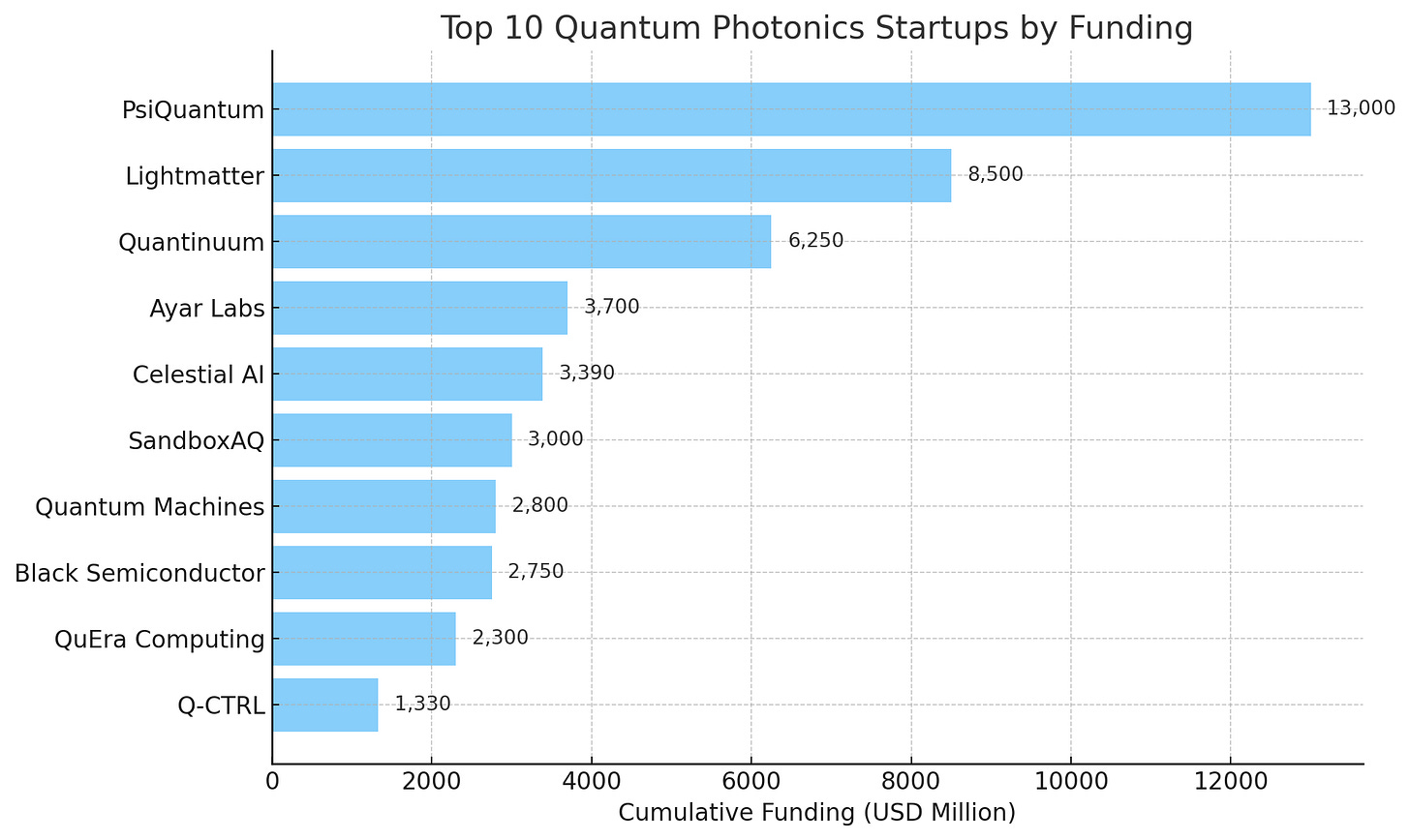
Over the past few years,quantum computing and photonics startupshave emerged as some of the hottest sectors for venture capital. FromPsiQuantum’s record $13B in cumulative fundingtoLightmatter’s $8.5B push into photonic computing, investors are betting heavily on technologies that can overcome the bottlenecks of Moore’s Law.
The trend reflects two key dynamics:
Quantumrepresents the long-term pursuit of next-generation computation, targeting breakthroughs in cryptography, optimization, and materials science.
Photonicsaddresses today’s most urgent challenge — energy efficiency and bandwidth in AI and data centers — with solutions like optical interconnects and photonic accelerators.
Together, these domains are reshaping the future of computing. Capital is flowing not just to ideas, but toinfrastructure that could define the next decade of AI and HPC.
- Latest Funding Round
InOctober 2024, Lightmatter completed itsSeries D financing, raising$400 millionat a valuation of$4.4 billion.
Lead Investor: T. Rowe Price, a leading U.S. asset management firm
Co-investors: Google Ventures, Fidelity, and several existing investors
This marks not only Lightmatter’slargest single funding roundto date but also a strong endorsement from top-tier capital markets of itstechnological maturity and commercialization potential.
As of Series D, Lightmatter has raised a cumulative$850 million across six funding rounds, rankingsecond in the photonics computing trackof SVTR’s (Silicon Valley Tech Review) AI Venture Capital Index — underscoring itsleadership position in emerging photonic computing.
- Historical Investors & Capital Background
Lightmatter has gained wide-ranging support fromventure capital firms, industry investors, and strategic funds, spanning semiconductors, defense, cloud computing, and the AI ecosystem:
Traditional VCs: Matrix, Spark Capital, Sequoia Capital, SIP Global Partners
Industry & Strategic Investors: Lockheed Martin Ventures, Hewlett Packard Enterprise
Institutional Capital: Viking Global Investors, Trajectory Ventures, Eastward Capital Partners
Specialized Funds: FAST (GettyLab’s investment arm)
Thisdiverse investor basereflects both the backing oftop-tier Silicon Valley VCsand thestrategic endorsement from semiconductor and defense industry stakeholders, greatly enhancing Lightmatter’s credibility across government, high-tech manufacturing, and enterprise markets.
- CEO’s Strategic Statement on the Funding
Following the Series D round,Lightmatter CEO Nicholas Harrisstated:
This may be thecompany’s final private funding round, suggesting Lightmatter is approachingcash-flow self-sufficiencyor preparing for anIPO stage.
By October 2024, the company had alreadysecured large-scale purchase commitments, which provided the confidence underpinning this round.
This milestone signals that Lightmatter hasmoved beyond pure R&Dand entered arobust commercialization phase.
- Industry Significance of the Valuation
With a valuation surpassing$4 billion, Lightmatter has become a“Unicorn+”in the photonic computing sector — second only to a handful of late-stage peers.
Capital markets are valuing not only the commercialization potential ofPassage (photonic interconnect)but also thedisruptive role of Envise (photonic AI accelerator)as a next-generation compute engine.
Compared to rivals such asAyar LabsandCelestial AI, whose funding totals are in the$300–400 million range, Lightmatter’slarger financing scale and higher valuationhighlight itsfaster path to market adoptionandgreater technical maturity.
Across six funding rounds, Lightmatter has raised$850 millionwith a current valuation of$4.4 billion, marking a critical inflection point towardindustrial-scale adoption.
The Series D round not only reflects market confidence but also aligns with:
Secured large-scale customer orders
Collaborations withAMD, NVIDIA, Intel, and Qualcomm
A strategic packaging partnership withAmkor
Together, these developments indicate that Lightmatter is no longer just aresearch-focused startup, but is rapidly evolving into acore infrastructure supplier for the AI era— with potential pathways to anIPO or strategic M&A exit in the coming years.

Key Opportunities
- Photonic Interconnect Technology
As Moore’s Law slows and traditional CMOS processes approach both physical and cost-efficiency limits,photonic interconnectsare emerging as a critical breakthrough for high-performance computing (HPC) and AI data centers.
Today, the greatest challenge in data centers is no longer the compute power of individual processors, but rather theinterconnect capacity between processors. As AI model sizes scale from tens of billions of parameters to trillions and beyond, interconnect demand is growingnonlinearly. While GPU and CPU compute performance increases at an annual rate of roughly13% (NVIDIA GPUs)and18% (Intel Xeon CPUs), interconnect requirements are expanding atfour times the pace of core compute growth, creating bottlenecks in latency, routing complexity, and power consumption.
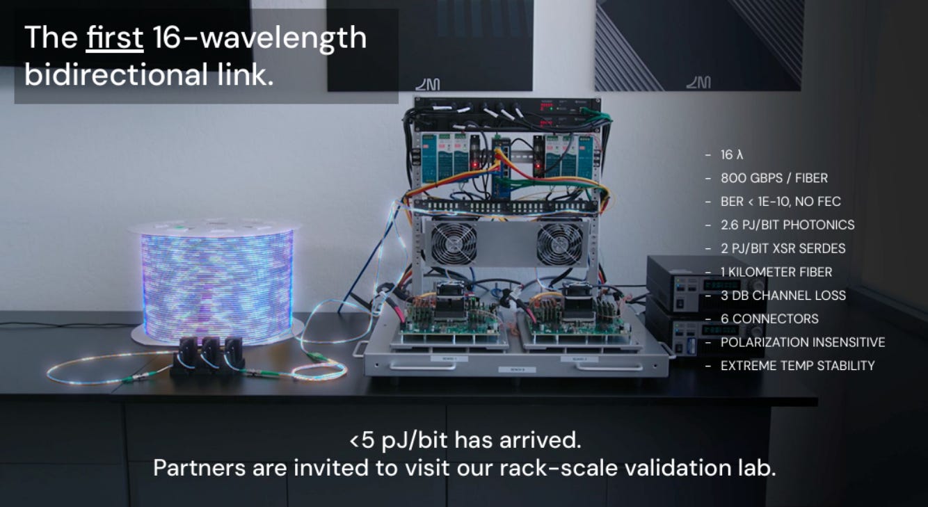
Lightmatter’sPassage technologydirectly addresses this pain point:
With16λ DWDM photonic interconnects, a single optical fiber can deliver800 Gbps of bidirectional bandwidth.
It can support the interconnect demands ofwafer-scale processors (WSEs), enabling data centers to function more likea single unified supercomputer.
Its high density and low energy consumption align closely with the trajectory ofArtificial General Intelligence (AGI)and evenArtificial Superintelligence (ASI).

This suggests that Passage is not merely a product but could evolve intoa foundational layer of future AI infrastructure.
- Next-Generation Chip Substrates
Lightmatter is also extending its reach intonext-generation chip substrates.
Chip substrates serve as thefoundation of all packaging, determiningsignal integrity (SI),power integrity (PI), thermal performance, and system reliability. As chip sizes grow ever larger (e.g., Cerebras’ wafer-scale processors), traditional silicon and organic substrates are struggling to support the requirements of high-speed, low-latencyopto-electronic integration.
Lightmatter’s strategy is to:
Develop substrates thatnatively support photonic interconnects, embedding optical waveguides and couplers directly into the packaging base layer.
Combine3D packaging with photonic channels, allowing a single substrate to host much larger chip modules.
Provide thephysical platformneeded formillion-node-scale AI clustersof the future.
If successful, this positions Lightmatter to secure afirst-mover advantage in system-level substrates, addressing a bottleneck that GPU and ASIC vendors are unable to resolve on their own.
- Laser Technology Innovation
Lightmatter is also exploring the feasibility ofchip-scale erbium-doped waveguide lasers (Er-doped waveguide lasers). While this technology has long been used in optical fiber communications, scaling it down to on-chip integration could deliver three major advantages:
Higher precision and efficiency— Er-doped lasers provide high coherence and stability, reducing signal errors during AI training processes.
Smaller size, greater scalability— Deep integration with photonic chips eliminates the need for bulky and power-hungry external laser arrays.
Lower cost— Compatibility with existing CMOS manufacturing enables better mass production potential and cost reduction.
The potential applications extend well beyond AI and data centers, spanningoptical communications, LiDAR, and precision sensing. This creates new growth avenues for Lightmatter, positioning the company not only in AI infrastructure but also in emerging markets wherecompact, efficient, and low-cost photonic lasersare becoming essential.
Key Risks
Limited Market Adoption
Although photonic computing and photonic interconnects hold tremendous technical potential, as of 2024 the market remains cautious:
High switching costs— Today’s data center ecosystem (GPU + CPU + Ethernet + InfiniBand) is already highly mature. Migrating to a photonic architecture requires hardware retrofitting, software adaptation, and operational process adjustments.
Lack of large-scale customer deployments— Lightmatter has not yet disclosed any hyperscale commercial customers in production, suggesting its products are still in transition fromtechnical validationtoindustry adoption.
The key challenge lies inlowering deployment barriersanddemonstrating overwhelming performance advantagesto break through market hesitancy.
Fundamental Limits of Photonic Computing in Logic Operations
Photonic computing is naturally well-suited forlinear algebra operations(matrix multiplications, convolutions), which align closely with AI training and inference. However, forgeneral-purpose computing, especially tasks involving control flow, conditional logic, and nonlinear operations, photonic computing faces inherent limitations.
Historical precedent— In the 1980s, Bell Labs attempted to develop “optical transistors,” but the technology failed to commercialize due to the uncontrollable nature of nonlinear optical interactions.
Lightmatter’s strategy is to focus on the domains wherephotonics excels(matrix-based computation), avoiding challenges in general-purpose workloads. This gives it an advantage inAI, quantum simulation, aerospace, and chemical modeling. Yet, if the market expects photonic computing toreplacegeneral CPUs/GPUs, a gap in expectations could emerge.
Technology Deployment & Supply Chain Challenges
Packaging and volume manufacturing— Photonic components (microring modulators, detectors, lasers) must be co-integrated with electronic chips in 3D packaging or hybrid bonding environments. Yield and consistency remain major hurdles.
Testing and validation— Photonic systems are far more complex to test than electronic ones, with few mature diagnostic or failure-analysis tools available, which could slow commercialization.
Capital intensity— Photonic computing requires heavy R&D and fab investment. Even though Lightmatter has raised$850 million, without rapid customer scaling, capital pressures remain high.
Lightmatter’s Core Opportunities vs. Challenges
Opportunities:
Break data center I/O bottlenecks withphotonic interconnects (Passage).
Build next-generation AI hardware foundations throughnovel substratesandon-chip lasers.
Deliverorder-of-magnitude gainsin energy efficiency and scalability.
Challenges:
Market adoption may proceed more slowly than anticipated.
Photonic computing’s applicability remains limited compared to general-purpose processors.
Technology deployment, manufacturing yields, and funding requirements carry ongoing risks.
Strategic Implication
Ultimately, Lightmatter’s future hinges on two critical proofs:
Winning large-scale hyperscaler deployments(AWS, Google, Microsoft, Meta).
Demonstrating “performance + cost” advantagessufficient to justify replacing or complementing the entrenched GPU-based ecosystem (NVLink, InfiniBand, Ethernet).
This will determine whether Lightmatter remains a niche innovator or evolves into acore supplier in next-generation AI infrastructure.
Silicon Photonics Integration: PIC and EIC Synergy
At its core, Passage 3D integratessilicon photonic circuits (PICs)withelectronic integrated circuits (EICs)to enable ultra-fast electro-optical conversion and data processing.
PIC design: Eight independent photonic modules, each with14 Tbpsof throughput, combining into massive aggregate capacity.
External ports: 16 optical ports, each delivering7.2 Tbps, connected internally by 256 fibers via FAUs (fiber array units), creating a dense internal optical fabric.
Device integration: Modulators, detectors, waveguides, and receivers are all monolithically integrated, allowing direct interfacing with existing short-reach SerDes and lowering deployment barriers.
A key enabler is themicroring modulator (MRM). Compact enough for dense integration, each channel supports50 Gbps. However, MRMs are extremely temperature-sensitive, with wavelength drift causing inter-channel interference. To counter this, Lightmatter developed aclosed-loop digital stabilization systemthat actively compensates thermal drift, maintaining error rates below10⁻¹⁰even under extreme conditions ranging from 25°C to 105°C.
Additionally, Passage 3D employs apolarization-insensitive design, enabling the use of cost-effective standard SMF instead of expensive polarization-maintaining fiber (PMF), significantly reducing capital costs and simplifying cabling.
Architectural Impact: Radix Expansion & Topology Optimization
The value of single-fiber 16λ BiDi lies in its ability to expand radix and optimize network topologies:
Radix expansion: Doubles connection density per port without adding more fibers, directly equivalent to higher radix for switches and GPUs.
Reduced hops: Higher radix lowers the required number of switch layers and hop counts for a given bandwidth.
Latency and energy efficiency: Fewer hops result in lower end-to-end latency and improved power efficiency—critical for communication-intensive AI training such asMixture of Experts (MoE)models.
Cost advantages: Reduces both fiber and switch requirements, cutting CAPEX and OPEX, while alleviating energy and space constraints in data centers.
In short, Lightmatter’s BiDi technology provides a way todouble network capacity without increasing physical resources—a direct path to building larger, higher-performance AI clusters without linearly scaling interconnect infrastructure.
Engineering Challenges Toward Industrialization
Despite its promise, several hurdles must be overcome before mass deployment:
Wavelength stability— Narrow DWDM spacing requires advanced thermal management and frequency-locking mechanisms.
Manufacturing consistency— Even minor deviations in silicon photonics processes can impact yield at such high channel density.
Thermal and reliability constraints— CPO packaging integrates optics and compute, demanding more rigorous thermal management and reliability assurance.
Nonlinear optical effects— High power densities can induce self-phase modulation and four-wave mixing, requiring compensation strategies.
The Inevitable Evolution of AI Interconnects
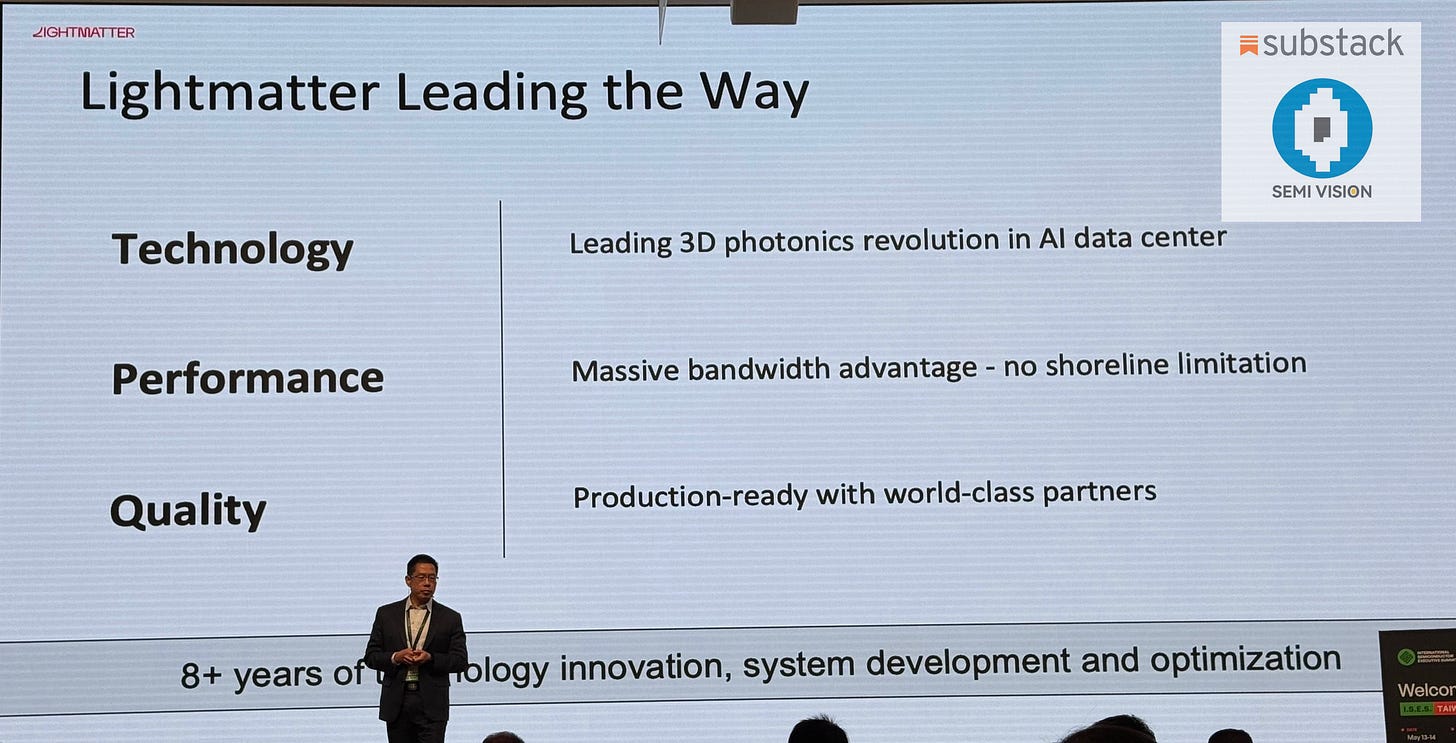
Lightmatter’s Passage 3D is not just about bandwidth—it represents anarchitectural innovation:
Achieving16λ DWDM per fiber, pushing single-fiber capacity to its limits.
Embeddingphotonics and electronics at the package level, reducing footprint while improving efficiency.
Optimizingsystem-level topology, lowering switch counts, cabling complexity, and latency.

This directly addresses the scaling bottlenecks facing AI clusters today, offering a practical pathway formillion-node XPU systems. As AI training workloads become increasingly communication-bound, interconnect efficiency may prove even more decisive than single-chip compute power.
The future growth of AI compute will depend less on electrons—and more onphotons. Passage 3D marks a milestone in that transition, ushering data centers into theera of photonic interconnects.
Doubling Down: World’s First 16-λ Single Fiber Bidirectional Link for AI

Comprehensive Comparison
Lightmatter: Focused onCPO + single-fiber DWDM, leading in bandwidth density and energy efficiency, making it the most targeted solution for data center I/O bottlenecks.
Ayar Labs: Specializes inOptical I/O (OIO), pursuing a low-power SerDes replacement path. It aligns closely with existing compute platforms but delivers more limited bandwidth gains.
Celestial AI: Emphasizesmemory disaggregation, tackling the problem from the system architecture layer. If successful, it could significantly reshape AI model computation.
Lightelligence: Positioned as anoptical accelerator, focusing on compute cores rather than interconnects. Its challenge lies in ecosystem adoption across hardware and software.
The four companies represent different branches of photonic technology:
Lightmatter and Ayar Labs→ focused on theinterconnect and packaging layer;
Celestial AI→ concentrated on thememory-network architecture layer;
Lightelligence→ targeting thecompute core layer.
Among them:
Lightmattershows the greatest breakthrough potential in bandwidth density and CPO commercialization;
Ayar Labsis the earliest to deploy low-power OIO;
Celestial AIcould redefine the AI memory wall challenge;
Lightelligenceoffers strong academic foresight but faces the steepest commercialization hurdles.






PreviousNext
TopLatestDiscussions








See all