How Do Advanced Packaging Equipment Vendors Tackle Challenges in a Globalized Market?
How Do Advanced Packaging Equipment Vendors Tackle Challenges in a Globalized Market?
- Source: SemiVision
- Author: SEMIVISION
- Published: 2025-08-25T16:40:02+08:00
- URL: https://tspasemiconductor.substack.com/p/how-do-advanced-packaging-equipment How Do Advanced Packaging Equipment Vendors Tackle Challenges in a Globalized Market?


How Do Advanced Packaging Equipment Vendors Tackle Challenges in a Globalized Market?
Original Article by SemiVision Research (TSMC,UMC,Samsung,Intel,ASML,AMAT, Lam,TEL,KLA,ASE,Amkor,JCET,Disco,Besi ,ASMPT,K&S,Semes,Hanmi,Hanwha, EVG,SUSS,Teradyne,SCREEN,Canon,Nikon,Lasertec)

Aug 25, 2025
∙ Paid

Global Semiconductor Foundries: Front-End WFE and Back-End Packaging Supply Chain Analysis – Facing Globalization Challenges
The race for advanced process nodes has madeWafer Fab Equipment (WFE)in the front-end, as well as back-end packaging equipment, increasingly critical for semiconductor foundries. Leading players such as TSMC, UMC, Samsung Electronics, and Intel control the world’s most advanced process technologies, yet they remain highly dependent on a globalized ecosystem of equipment and materials suppliers. Entering the AI and high-performance computing (HPC) era, demand for advanced packaging platforms—including 2.5D/3D packaging, Hybrid Bonding, and CoWoS—is surging, reshaping the back-end equipment landscape. This paper analyzes the core elements of both WFE and back-end packaging supply chains, while exploring how equipment vendors are responding to the challenges of geopolitics and globalization.
As Moore’s Law slows, advanced packaging has emerged as the key pathway to sustaining semiconductor performance gains. Technologies such as 2.5D/3D packaging, heterogeneous integration, Hybrid Bonding, high-density substrates, and chip stacking not only test equipment suppliers’ capabilities in precision, yield, and material integration but also place them at the center of a complex global market environment. On one hand, equipment vendors must meet the stringent demands of top-tier foundries like TSMC, Samsung, and Intel for next-generation packaging. On the other, they must adapt to geopolitical pressures, government-driven semiconductor self-sufficiency policies, and supply chain diversification trends. Striking a balance between technological breakthroughs and fragmented markets will determine whether advanced packaging equipment suppliers can maintain leadership on the global stage.

2025年8月10日
In the global semiconductor supply chain, the front-end WFE (Wafer Fab Equipment) and back-end advanced packaging supply chains are increasingly characterized by a dual dynamic of “technological concentration” and “geographic diversification.”
In front-end wafer manufacturing, the sector is almost monopolized by five major players—ASML, Applied Materials, Lam Research, Tokyo Electron (TEL), and KLA—on which foundries such as TSMC, Samsung, Intel, and UMC are highly dependent. While U.S. and Dutch firms remain global leaders in lithography, deposition, and etching, export controls and policies such as the CHIPS Act and the European Chips Act have compelled equipment suppliers to adjust their footprints, establishing new production and service bases across North America, Europe, Japan, and Southeast Asia to strengthen supply chain resilience. Meanwhile, although China’s domestic equipment vendors are rapidly catching up, they currently satisfy less than 14% of back-end demand, making it difficult in the short term to challenge the dominance of international giants.
In the back-end packaging domain, the rise of AI and HPC applications has pushed 2.5D/3D packaging, Hybrid Bonding, andTCB(Thermal Compression Bonding) into the spotlight. The OSAT market is dominated by ASE, Amkor, and JCET, while Disco, Besi, ASMPT, K&S, and Semes form the backbone of the equipment supply chain. For TSMC, CoWoS and SoIC have become critical platforms for driving HPC packaging, which in turn has spurred the development of new materials and technologies such as glass substrates and Hybrid Bonding. Looking forward, as reticle size limitations create bottlenecks,SoW(System-on-Wafer) andCoPoS(Chip-on-Panel-on-Substrate) are expected to gradually replace traditional CoWoS, with glass substrates potentially emerging as the next breakthrough. In this environment, equipment suppliers not only face cost and pricing pressures but must also address challenges related to sustainability, customization, and global competition. Only through technological innovation, product diversification, localized investment, and cross-border collaboration can they maintain leadership and seize the next wave of growth.

2025年7月13日
In the semiconductor industry, advanced logic processes will remain concentrated among a few dominant players, but advanced packaging opens the door for niche companies with specialized technologies to emerge. At the same time, this shift creates a significant opportunity for specialty chemicals, as it represents a transformation pathway from traditional chemical industries into the semiconductor supply chain. In Taiwan, this localization trend has already given rise to many companies pivoting from conventional chemicals to semiconductor materials, including advanced photoresists, molding compounds, underfills, BARC, and ARC.
We are seeing new innovative materials emerging across CoWoS, HBM, and silicon photonics. Therefore, in the future, the semiconductor industry will need to shift its mindset toward the integration of materials as a core consideration.
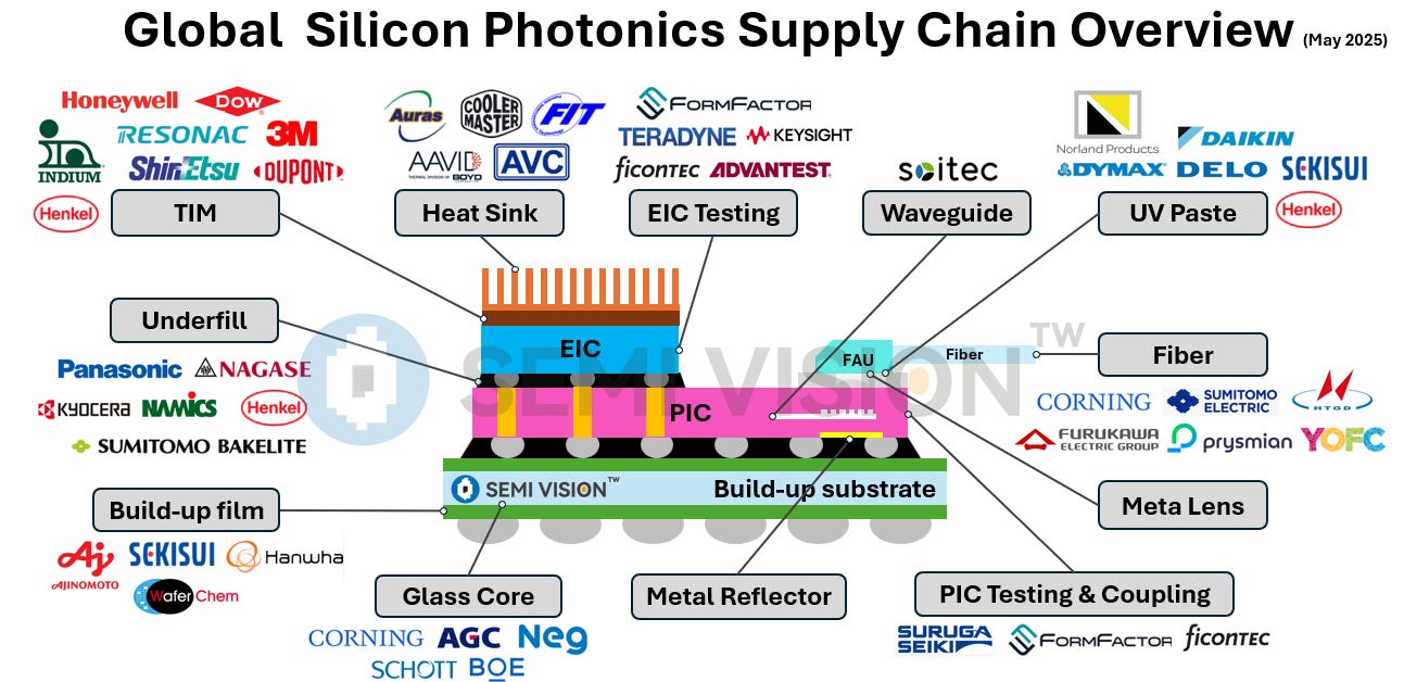
While semiconductor supply chain analysis has traditionally focused on equipment,materials are becoming a critical area of discussion. For example:
In theCoWoS supply chain, we see multiple material suppliers involved.
InOptical Engines, UV resins are being used to connect FAUs (Fiber Array Units) and optical modules.
InHybrid Bonding, specialized adhesives are applied at wafer edges to prevent wafer sliding during wafer-on-wafer (WoW) processes.
Inthermal management, the evolution of TIM (Thermal Interface Materials) has introduced new solutions.
This signals a gradual paradigm shift in semiconductors—from equipment-centric to material-centric innovation.
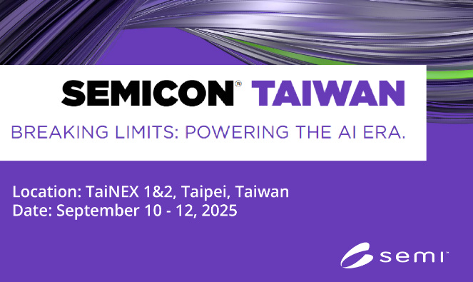
At the upcomingSEMICON Taiwan, numerous equipment vendors are expected to release updates on their latest technologies, illustrating this shift with concrete examples.
SemiVision has compiled a series of important semiconductor suppliers that are well worth exploring. More detailed insights will be prepared and shared with our members.
This article will reference several relevant companies within the semiconductor industry.
TSMC, UMC, Samsung Electronics, Intel, ASML, Applied Materials (AMAT), Lam Research, Tokyo Electron (TEL), KLA, ASE (Advanced Semiconductor Engineering), Amkor, JCET, Disco, Besi (BE Semiconductor Industries), ASMPT (ASM Pacific Technology), Kulicke & Soffa (K&S), Semes, Hanmi, Hanwha, EVG (EV Group), SUSS MicroTec, Teradyne, SCREEN, Canon, Nikon, Lasertec, Kokusai Electric, NAURA, AMEC, Kingsemi, Huaxing, ACM Research, SK hynix, Broadcom, Marvell, Huawei, SMIC, Sony, Denso, Toyota, NVIDIA, Rapidus

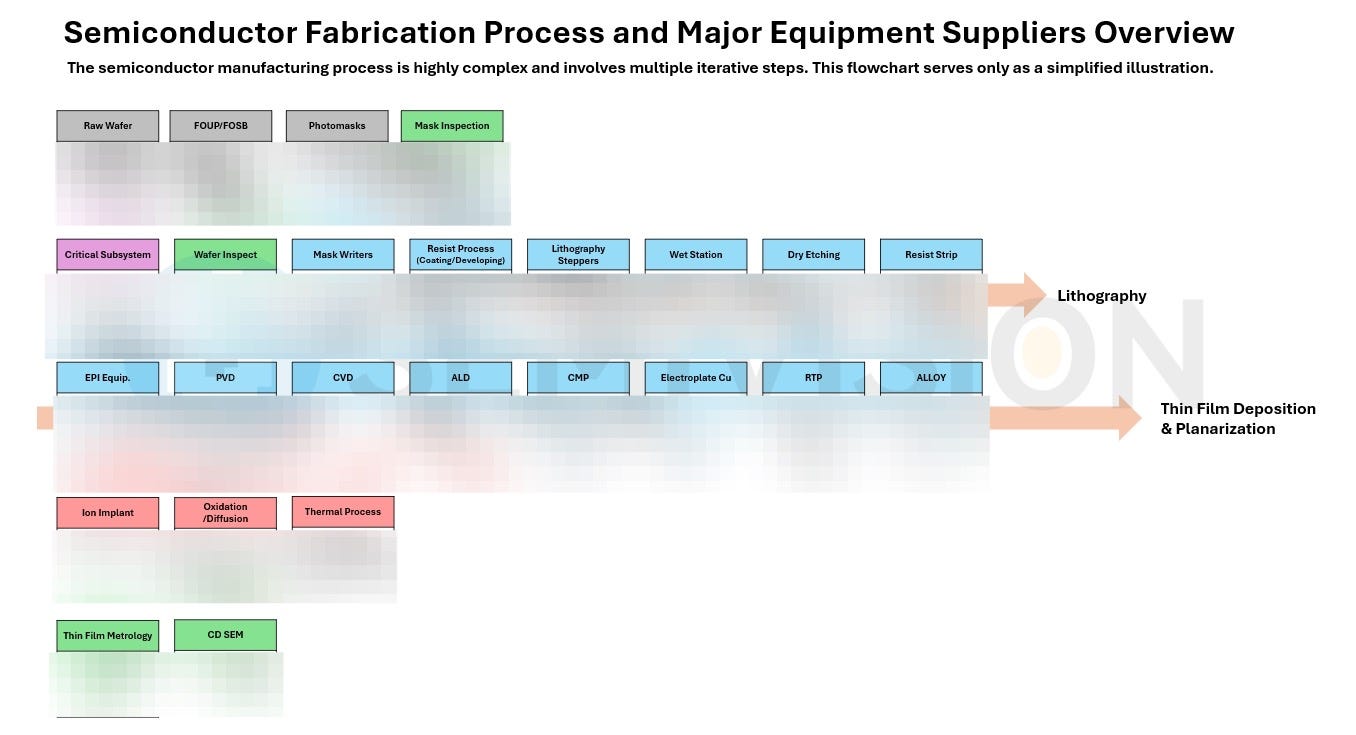
For Paid Members, SemiVision will discuss topics on
Future Development Directions of the Semiconductor Industry
Overview of the Front-End WFE Supply Chain
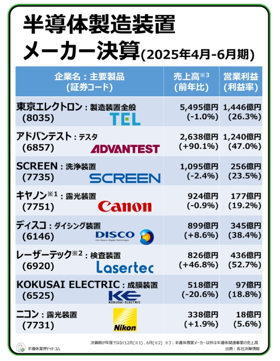
WFE Market Size and Leading Vendors (KE, Lasertec, DISCO, Canon , Nikon, SCREEN, TEL)
Macro Commentary in Semiconductor Industry
Kumamoto’s Second Take-Off: From “Silicon Island” to Semiconductor Revival
Wafer Fab Equipment (WFE) Supply Chain Configuration
Back-End Packaging Equipment and OSAT Supply Chain
Backend Equipment Vendors and Market Share
Advanced Packaging Market Trends and Demand
Supply Chain Strategies in a Globalized Environment
Foundries and OSATs’ Strategies
Impacts and Outlook Amid Globalization Challenges
Global Semiconductor Supply Chain
CoWoS Supply Chain Complexity
Positioning and Limitations of CoWoS
CoWoS Supply Chain and the Rise of Glass Substrates
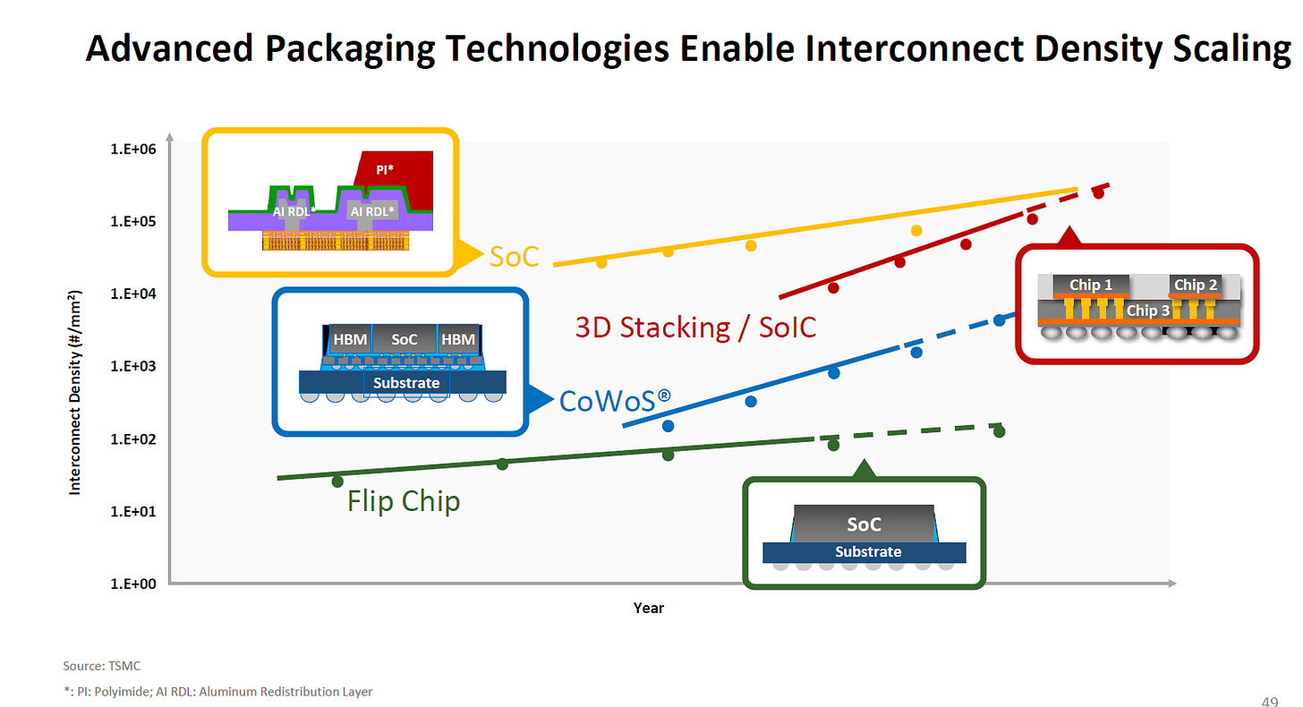
Interconnection Density as a Packaging Evaluation Metric
SoIC: Capacity and Challenges
Environmental and Sustainability Pressure
Cost and Price Sensitivity in advaced logic node
From Silicon Island to AI Supply Chain
Advanced Packaging and Silicon Photonics Integration
From Copper Interconnects to Optical Interconnects: Materials and Physical Limits
Nonlinear Optics and Material Innovation


Future Development Directions of the Semiconductor Industry
Front-End WFE vs. Back-End Advanced Packaging: A Dual-Axis Trend
The semiconductor ecosystem is increasingly showing adual-axis pattern:
“Technological concentration × geographically dispersed capacity and services.”
Front-End (WFE):Dominated by a handful of players—ASML, Applied Materials (AMAT), Lam Research, Tokyo Electron (TEL), and KLA.
Back-End (Advanced Packaging):Led by OSAT majorsASE, Amkor, JCET, along with key equipment vendors such asDisco, Besi, ASMPT, K&S, and Semes.
The surge ofAI/HPCis driving demand for2.5D/3D integration, Hybrid Bonding (HB), and TCB, which are now the primary growth engines. Meanwhile, the supply chain is acceleratinglocalization across Taiwan, the U.S., Japan, Europe, and Southeast Asiato hedge against geopolitical risks and export controls.

Moore’s Slowdown → Packaging Takes the Lead
With Moore’s Law slowing,advanced packaging has become the primary vector for performance scaling.
CoWoS and SoICare now the main technological pathways.
However,reticle size limits (~9.5X)and rising cost pressures are pushing the industry to exploreSoW/CoPoS architectures, glass substrates, and TGV (Through-Glass Vias)as the next expansion frontier.
Interconnect Density as the Core KPI
TraditionalCoWoSis constrained by micro-bump pitch at ~40 µm.
SoIC with Hybrid Bondingcan achieve ≤10 µm, enablinghigher bandwidth, lower latency, and lower power consumption.
Challenges remain: test accessibility, wafer thinning & warpage, and long-term reliability validation.
From Equipment-Centric to Materials-Centric
As packaging complexity rises,materials integration becomes the new battleground:
UV-curable resins for optical engines.
Edge anti-slip adhesives for HB.
Advanced thermal interface materials (TIM).
Low-Dk, low-CTE dielectric substrates.
The ability tointegrate differentiated materialswill increasingly define competitiveness.
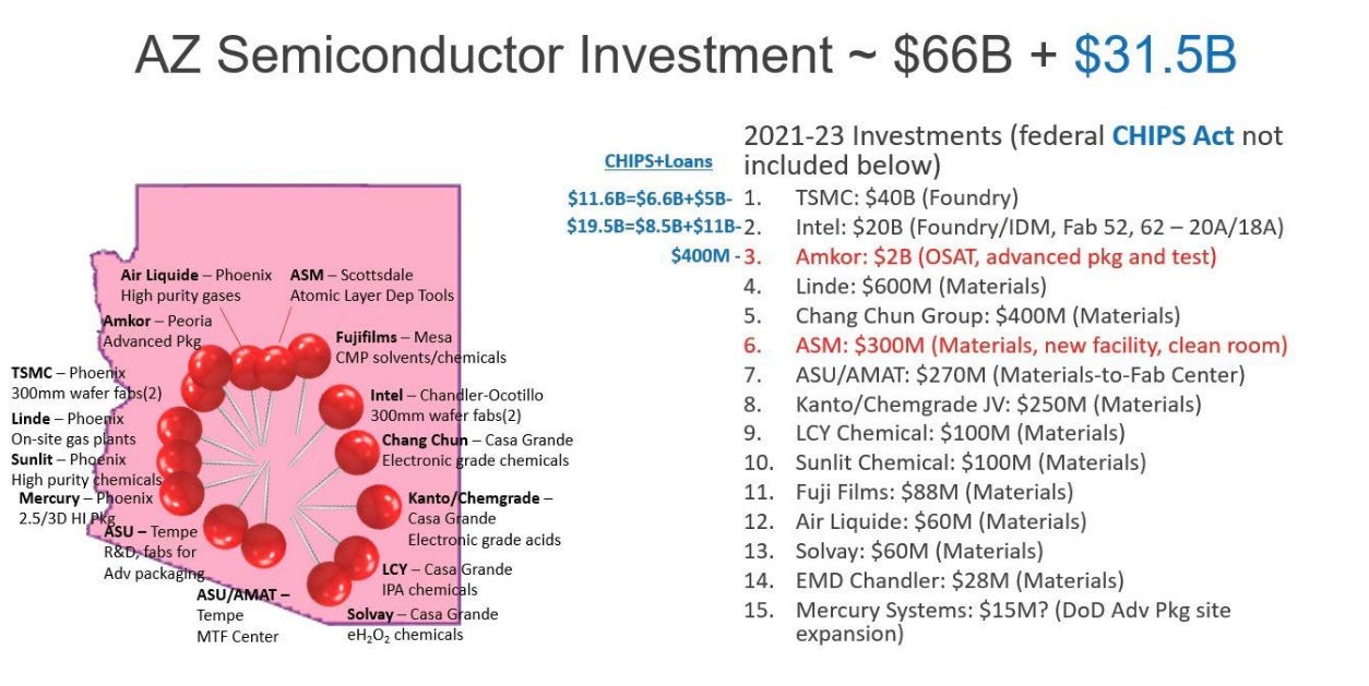
Geopolitics Reshaping the Supply Chain
Export controls + CHIPS Act + EU Chips Actare driving suppliers and fabs towardglobal diversification and regional proximity.
China is boosting equipment penetration, but in the near term it remains difficult to displace global incumbents.
Green Manufacturing as a Hard KPI
Sustainability has becomeembedded into cost and efficiency metrics.
Example:TSMCis acceleratingRE100 targets, supply chain carbon reduction, and long-term renewable power procurement.
ESG is no longer optional—it is now structurally tied toprocess efficiency and cost competitiveness.
Key Takeaways
Moore’s slowdown → Packaging as the growth engine.
CoWoS/SoIC dominate, while SoW/CoPoS, glass substrates, and TGV represent the next frontier.
Interconnect density = core KPI.
Moving from ~40 µm micro-bumps (CoWoS) to ≤10 µm hybrid bonding (SoIC+HB).
Gains in bandwidth, latency, and power efficiency, but new reliability challenges.
Shift from equipment → materials.
Materials for optical engines, HB adhesives, advanced TIM, and low-Dk dielectrics become strategic differentiators.
Geopolitics reshaping supply chains.
Export controls + subsidies acceleratelocalized, resilient ecosystems.
China’s share is growing, but still far from replacing global leaders.
Green manufacturing as a hard requirement.
ESG and RE100 goals embedded into efficiency and cost structures.
Supply Chain Landscape and Market Dynamics
Front-End WFE:
The market is dominated by five giants (ASML, AMAT, Lam, TEL, KLA). In 2024, WFE revenue was approximatelyUSD 13.3B, projected to reachUSD 16.5B by 2029. In the past two years,China has emerged as one of the largest destinations for shipments, driving suppliers to expand global service and manufacturing nodes.
Back-End Packaging:
The rise ofAI/HPCworkloads is fueling demand forHB, TCB, and HBM. Equipment vendors includingBesi, ASMPT, K&S, Semes, Hanmi, Hanwha, EVG, and SUSSare ramping up capacity and upgrading product lines. By 2030, theTCB equipment marketis estimated at ~USD 936M, whileHB equipmentis projected at ~USD 397M.
Metrology & Inspection:
KLAcontinues to dominate, whileHitachi’s CD-SEMremains the industry benchmark.
Technology Roadmaps and Bottlenecks
Platform Competition:
TSMC:3D Fabric (CoWoS/SoIC).
Samsung:CUBE Platform.
Intel:EMIB/Foveros.
OSATs:ASE, Amkor, JCET as key players.
TSMC Node & Systemization:
Transition fromN3 → N2, alongsideA16 (BSPDN/SPR)andA14.
Use ofTransformer Flowto reduce design migration costs.
System Technology Co-Optimization (STCO) througheDTC, IVR, IPD, MIM, MtMat the component level.
Optical Interconnects & Materials:
Copper interconnects are approaching physical limits.
CPO/LPO and PIC-EIC hybrid bondingare accelerating.
Nonlinear optics (TFLN, III-V, LN)represent mid- to long-term breakthroughs, but face hurdles in contamination control, yield, and cost.

2025年5月31日
Geopolitics and Localization
Export controls + subsidies(CHIPS Act, EU Chips Act) are pushing suppliers to build fabs and service hubs inNorth America, Europe, Japan, and Southeast Asia.
Leading fabs (TSMC, Samsung, Intel, UMC) are expanding globally while investing heavily inin-house advanced packaging R&D.
China:actively pursuing localization, focusing in the short term on substitution and scenario-driven adoption.
Japan:revival led byRapidus, strengthening domestic equipment, metrology, and materials. TheKumamoto projectillustrates a dual economic + geopolitical demonstration effect.
Company Observations
TEL:Near-monopoly in track systems; expanding intoGAA/BSPDN; reinforcing SoIC/Hybrid Bonding capabilities.
Advantest:Duopoly with Teradyne in ATE; AI/HBM demand driving CP/FT/SLT growth.
SCREEN:GAA/SPR boosting demand for advanced wet cleaning.
Canon/Nikon:Focused on mature nodes and panel-level lithography; ASML retains EUV monopoly.
DISCO:Central in wafer thinning and dicing; warpage mitigation requires joint material + process innovation.
Lasertec:Near-monopoly in EUV mask inspection.
Besi/ASMPT/K&S/Semes:Key roles in hybrid bonding, die attach, automation integration, TCB, and Korean supply chain ecosystems.
Costs and Sustainability
Rising cost curve:
N2 wafers:~USD 30K.
2 nm fab CAPEX:~USD 27–28B.
Driving interest inCoPoS/CoWoP architectures, cost/area-efficient solutions, and advanced automation/digitalization.
ESG Execution:
AcceleratedRE100 timelines, green power purchase agreements, Scope 1/2 net-zero goals across global sites.
Sustainability is now embedded as ahard procurement and customer requirement.
Risks and Opportunities
Risks:
Export controls & tariffs.
Overlapping investments due to regionalization.
Yield and metrology challenges in HB/TCB.
Cross-contamination and cost uncertainty in new material adoption.
Opportunities:
Technology bets:HB/TCB, glass substrates/TGV, backside power delivery (SPR/PowerVia equipment), advanced precision metrology.
Supply chain strategy:Multi-region manufacturing + nearshoring, collaboration with imec/Leti to shorten POR cycles.
Materials innovation:UV resins, edge anti-slip adhesives, advanced TIM, low-Dk/low-CTE dielectrics, optoelectronic-compatible packaging materials.
Business model innovation:Modular and platformized product lines, custom ASIC and multi-package support, automation/digitalization to reduce cost.
Structural Outlook
Short-term volatility, long-term strength:AI/HPC demand provides structural support, making advanced packaging the next battleground.
Blurring boundaries:Front-end and back-end equipment, materials, design/packaging/testing are converging into cross-domain collaboration and M&A.
Winning formula:Companies that integratetechnological innovation × materials leadership × global-localized supply chains × ESG executionwill secure outsized market share in the next cycle.
Overview of the Front-End WFE Supply Chain
WFE Market Size and Leading Vendors (KE, Lasertec, DISCO, Canon , Nikon, SCREEN,TEL)
According to leading research institutes, global WFE vendor revenue in 2024 is estimated at USD 13.3 billion, of which 83% comes from equipment shipments and 17% from services and maintenance. By 2029, the market is projected to reach USD 16.5 billion. The recognized leaders in the WFE market are ASML, Applied Materials (AMAT), Lam Research, Tokyo Electron Limited (TEL), and KLA. These companies are mainly headquartered in the U.S., Japan, and the Netherlands. While U.S. vendors have historically led in revenue share, in 2023–2024 China became the largest destination for equipment shipments, accounting for nearly one-third of global WFE revenue.
Key Global Semiconductor Equipment Companies
Tokyo Electron (TEL):
TSMC’s EUV/DUV fabs heavily rely on TEL’s coating/develop (track) systems. TEL’s official disclosures highlight collaborative R&D on GAA and BSPDN (Backside Power Delivery). TEL commands ~90% track market share and ranks among the top in deposition/etch/cleaning tools. Having missed opportunities in CoWoS, TEL is now aggressively expanding into SoIC bonding technologies, recognizing their broad applicability to 3DIC and future 4D packaging.

Advantest:
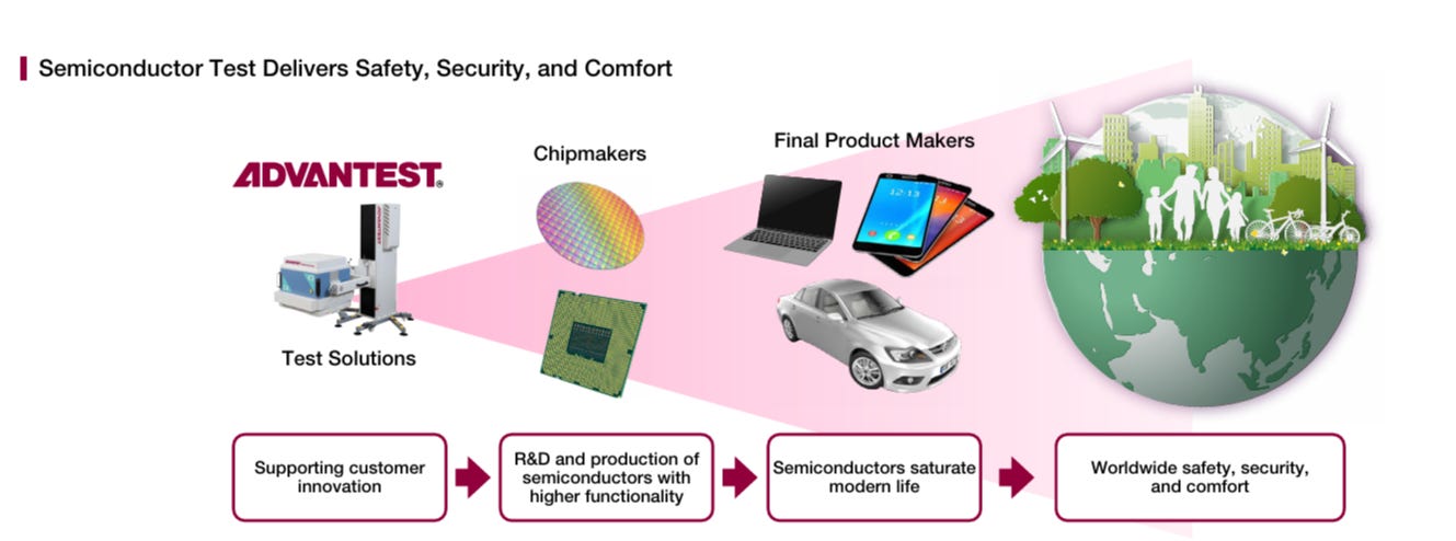
With HBM and AI server demand surging, wafer sort, final test (FT), and SLT requirements are rapidly growing. Together with Teradyne, Advantest forms a duopoly (>80% market share) in ATE. Testing for SoIC (WoW/D2W) integration remains challenging, particularly for TSV probing after stacking, reinforcing the entry barriers for other suppliers.
SCREEN:
A global leader in wafer cleaning (batch/single-wafer), SCREEN is poised to benefit from A16 (SPR) backside processes. The transition from FinFET to GAA architectures significantly increases the importance of wet clean steps, particularly in complex FET structures where sidewall defects can severely impact yield.

Canon / Nikon:
Focused on KrF / i-line lithography for TSMC’s mature and specialty nodes, while ASML dominates EUV for leading-edge. In packaging, DUV demand remains steady, with Canon developing panel-level lithography tools. For CoPoS, however, POR vendors currently dominate the lithography supply chain.

DISCO:
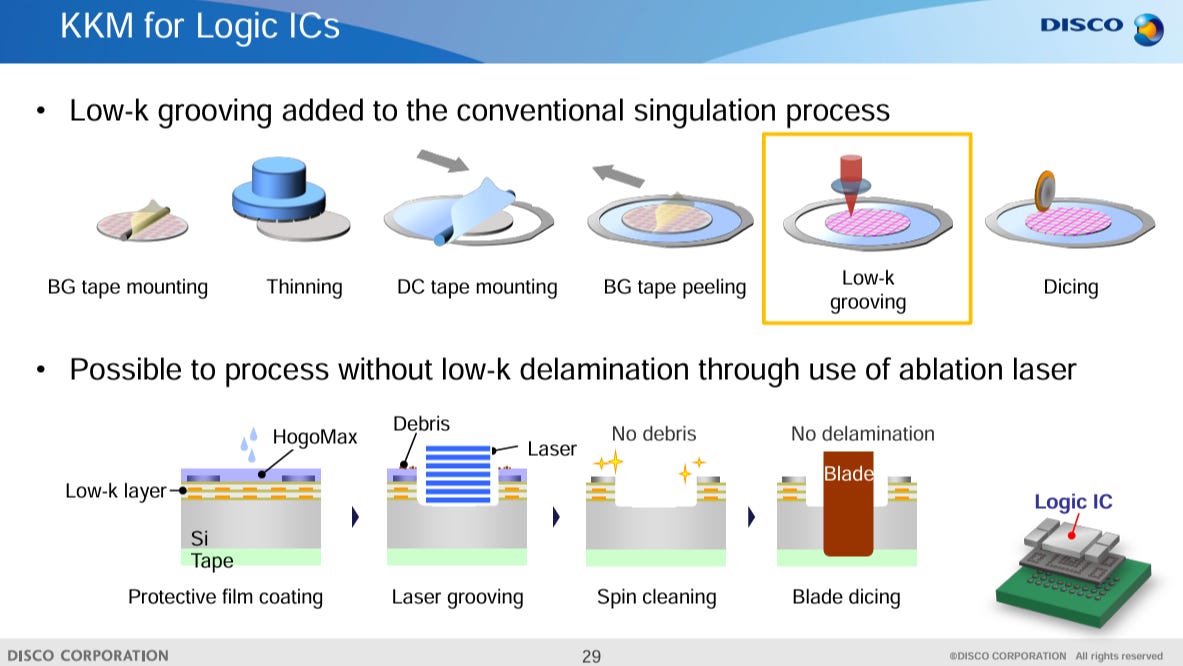
Provides critical dicing, DBG (dicing before grinding), and thinning solutions for TSMC’s CoWoS/SoIC and HBM stacking. As wafers are typically thinned from ~750 µm to ~100 µm for silicon interposers, DISCO’s grinding tools are indispensable. Yet thinning introduces warpage challenges—more severe in CoWoS-L than CoWoS-R, due to the integration of RDL, LSI, eDTC, IVR, molding, and complex materials. TSMC has demonstrated advanced warpage mapping in CoWoS-R (2025 ECTC), but CoWoS-L remains more challenging due to stronger material-property-driven warpage effects. Potential mitigations include thermal treatments, oxide/metal deposition, and optimized material stacks.
Lasertec:
Holds a near-monopoly (~100%) in actinic EUV mask inspection, making it indispensable for TSMC’s EUV and High-NA adoption. In EUV inspection, Lasertec and KLA form a two-player dominance across complementary categories.

Kokusai Electric:
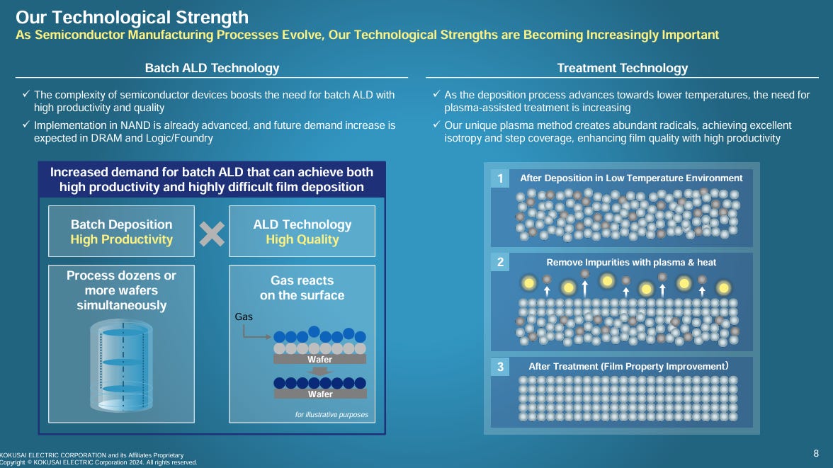
A global leader in batch ALD/LPCVD, diffusion, and annealing tools, widely adopted across logic and memory nodes. TSMC continues to use Kokusai’s deposition tools across multiple process generations.
Macro Commentary in Semiconductor Industry
China is projected to be the largest WFE demand market in 2024 (40%), with rising domestic equipment penetration. However, advanced lithography remains constrained. This trend affects demand for Canon/Nikon (mature lithography) and SCREEN (cleaning tools), while also pushing Japanese suppliers to accelerate regional diversification and local service expansion.

2025年7月19日
Currently, Japan is actively strengthening its domestic semiconductor supply chain through projects such as Rapidus, which aims to achieve 2nm process mass production by 2027. This ambitious goal requires extensive support from process equipment, metrology, and materials. As a result, Japanese semiconductor equipment vendors such as TEL (Tokyo Electron), Advantest, SCREEN, Lasertec, and DISCO are playing increasingly critical roles in the global supply chain. These companies are not only core suppliers to leading foundries such as TSMC, Samsung, and Intel, but also serve as the “localization pillars” of the Rapidus program, providing essential equipment ranging from coating and lithography tracks, cleaning, thinning and dicing, testing and inspection, to EUV mask inspection.
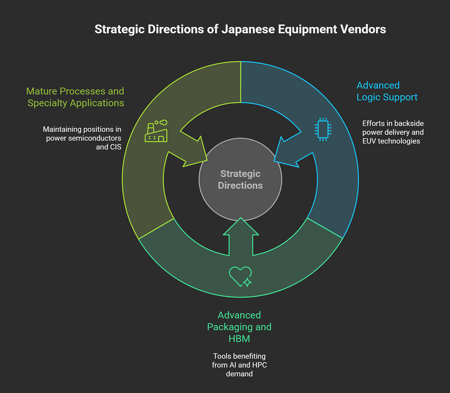
Looking ahead, the strategic directions of Japanese equipment vendors will focus on three areas:
Advanced Logic Support: With the introduction of GAA and SPR, Japanese vendors are ramping up efforts in backside power delivery, ultra-thinning, double-sided alignment exposure, and EUV/High-NA inspection technologies.
Advanced Packaging and HBM: DISCO’s thinning and dicing tools and Advantest’s testing platforms are direct beneficiaries of AI and HPC-driven demand for advanced packaging.
Mature Processes and Specialty Applications: Canon and Nikon continue to supply KrF/i-line lithography tools, while also maintaining strong positions in power semiconductors and CIS, consolidating their role in mature nodes and localized supply.
Overall, Japanese equipment makers are enhancing their global influence through partnerships with TSMC and Intel, while also leveraging the localization momentum driven by Rapidus to secure a solid position in the next generation of advanced process technology.

Source: The Economist
Kumamoto’s Second Take-Off: From “Silicon Island” to Semiconductor Revival
Kumamoto, once proudly known as Japan’s“Silicon Island,”is experiencing an unexpected second act. For decades, the region was home to a cluster of semiconductor factories and electronics suppliers, but much of that glory faded as production shifted overseas. Now, with TSMC’s multibillion-dollar investment and its partnerships with Sony, Denso, and Toyota, Kumamoto is reclaiming its place on the global technology map.
The changes are tangible. Job opportunities are surging, with thousands of new positions opening not only in fabs but across supporting industries, from logistics to construction. Infrastructure is expanding rapidly—roads, housing, and utilities are being modernized to support the influx of workers and their families. The local economy, once stagnant, now hums with the energy of a region being rewired for the future.
Beyond economics, there is a subtle cultural blending taking place. Taiwanese influence is visible on the ground, from supermarkets selling pineapple cakes and bubble tea, to bilingual “Welcome” signs in Chinese and Japanese. For many residents, this cross-cultural exchange is a reminder that the semiconductor industry is not just about chips, but about the movement of people, knowledge, and culture.
Strategically, Japan views Kumamoto’s revival as part of its broader attempt to reclaim relevance in the semiconductor race. Bolstered by generous government subsidies and aligned with the strategic needs of allies like the United States, this project aims to ensure that chipmaking capacity is not concentrated in a single region. By diversifying production beyond Taiwan, Japan contributes to a more resilient global supply chain—a critical priority as geopolitical risks threaten the world’s most vital industry.

If successful, Kumamoto could become the symbol of Japan’s “semiconductor second take-off.” It is a model of how advanced manufacturing reshapes not only local economies but also national strategy, demonstrating that industrial revival can carry both economic dividends and geopolitical weight. In this sense, Kumamoto is more than a regional success story; it is a test case for how democracies can rebuild technological sovereignty in an era of fragile supply chains and intensifying competition.
Wafer Fab Equipment (WFE) Supply Chain Configuration
Major foundries remain highly dependent on a small group of international suppliers. Due to high technological barriers and capital intensity, only five global giants provide the majority of WFE tools. The following table (based on public information) summarizes the key equipment suppliers forTSMC, UMC, Samsung, and Intel:
Globalization Challenges
Geopolitics and Export Controls:
The U.S. and its allies have imposed restrictions on exporting advanced lithography machines and certain semiconductor manufacturing equipment to China, particularly ASML’s EUV systems. This has forced equipment suppliers to diversify markets and revenue streams. Tokyo Electron (TEL) disclosed that export restrictions reduced its China revenue share to ~30%, but strong demand for advanced nodes from other regions remains. Meanwhile, U.S.–China trade tensions have led governments to introduce subsidies such as theCHIPS Actand theEuropean Chips Actto attract local fabs, significantly reshaping the equipment supply chain.
Market Volatility and AI-driven Equipment Demand:
While mainstream consumer electronics recovery remains sluggish, AI and HPC demand has boosted adoption of 2.5D/3D packaging and HBM (High Bandwidth Memory). As a result,Thermo-Compression Bonding (TCB)andHybrid Bondinghave become critical technologies. WFE vendors, facing demand volatility, are expanding product portfolios and application coverage to sustain revenue. BothHBMandCoWoSrequire robust bonding solutions.
China’s Catch-Up and Localization Push:
Domestic Chinese equipment vendors currently meet only about14%of back-end equipment needs. While government policy and funding are accelerating local capability, they cannot yet replace international suppliers in the short term. To address localization requirements, vendors are setting up new manufacturing and service bases outside China—in the U.S., Europe, Japan, and Southeast Asia. Most suppliers rely on geographical diversification, local production, and strategic technology partnerships to mitigate tariff and logistics risks.
Back-End Packaging Equipment and OSAT Supply Chain
Packaging Processes and Equipment Categories
Back-end packaging includes wafer preparation, interposer fabrication, die attach, underfill, solder ball/paste attach, molding, dicing, and testing. Based on SemiVision Research’s process classification, the following summarizes key steps, market characteristics, and suppliers:


Five Major Suppliers in Control:
By 2025, the WFE market will remain dominated byASML, Applied Materials, Lam Research, Tokyo Electron (TEL), and KLA, together accounting for more than70% of total revenue. Each company holds leadership in different segments:
ASMLmonopolizes EUV lithography,
Applied Materialsleads in deposition and ion implantation,
Lam Researchis ahead in dry etch, electroplating, and dry strip,
TELhas absolute strength in coater/developer tracks and diffusion furnaces,
KLAcommands 56%–85% market share in process control and optical inspection.
China’s Rapid Catch-Up:
With strong government support,NAURA, AMEC, Kingsemi, and Huaxingare actively developing dry etch, ALD, PVD, CMP, and cleaning equipment. While their current global market share in most sub-segments remains in the single digits, adoption rates at domestic foundries are rising. By 2025, Chinese suppliers are expected to capture5%–10%market share in areas such as single-wafer cleaning, dry etch, PVD, and ALD.
Rising Demand for Backend Packaging and Copper Plating:
The growth ofHBM and 2.5D/3D packagingis driving rapid increases in demand for electroplating, CMP, and cleaning tools. Suppliers such asLam
Research and ACM Researchare accelerating shipments, with the related market expected to see aCAGR above 9%.
Increasing Importance of Metrology and Inspection:
As process nodes advance to2 nm and GAA (Gate-All-Around) structures, precision requirements for optical and e-beam inspection tools have sharply increased.KLAcontinues to strengthen its leadership through optical, e-beam, and scanning X-ray solutions, whileHitachi CD-SEMhas established itself as the industry standard with a70% market share.
Total (Top 10 combined): USD 41.56 billion, with YoY growth of 3%.

Currently, the foundries offering comprehensive advanced packaging platforms are mainly concentrated inTSMC’s 3D Fabric Platform,Samsung’s CUBE Platform, andIntel’s EMIB and Foveros Platforms.

2025年5月1日
ASE (Advanced Semiconductor Engineering) also provides a highly comprehensive advanced packaging platform. In addition, ASE has entered the field ofSilicon Photonics with CPO (Co-Packaged Optics) technology. Beyond that, ASE has also developed certainpower-related technologies, including applications involtage regulators.
Furthermore, ASE has extended itsPoP (Package-on-Package)technology intoCPO applications, showcasing its ability to innovate across different domains of advanced packaging.


2025年6月18日
Backend Equipment Vendors and Market Share
Based on projections for2024–2025, the backend equipment sector has consolidated into atop five leading players:
Disco– Specialized in wafer thinning, grinding, and dicing, holding a20% market share in 2023. ItsTaiko thinning and dicing technologiesare critical for advanced packaging. TheTaiko waferis a highly specialized process, widely adopted by foundries, particularly forBGBM (Backside Grinding Backside Metallization)applications.
Besi (BE Semiconductor Industries)– Known fordie attach and hybrid bonding tools, with a~11% market share. Recently,Applied Materials acquired a 9% equity stakein Besi, highlighting the importance of heterogeneous integration.
ASMPT (ASM Pacific Technology)– With a9% market share, ASMPT offers a broad portfolio of backend equipment, focusing heavily onautomation and system integration.
Kulicke & Soffa (K&S)– Holds8% market share, a leader inwire bonding and die bonding equipment, and actively developingTCB (Thermo-Compression Bonding)technology. ItsFlexless TCBtechnology is a key focus area. Currently, K&S uses aformic acid process, but also aligns withplasma clean approaches.
Semes– A Samsung subsidiary with a5% market share, offering diverse backend equipment and maintaining a strong position in theKorean market.
Other growing suppliers include Hanmi, Hanwha (Korea), EVG (Austria), and SUSS MicroTec (Germany). Meanwhile, OSATs like Amkor are expanding advanced packaging capacity, while equipment makers such as Hanmi, Semes, Hanwha, K&S, and ASMPT are scaling up their TCB capabilities to meet surging AI-driven demand.
2025年7月13日
Advanced Packaging Market Trends and Demand

AI and HPC Driving 2.5D/3D Packaging
The demand for AI and high-performance computing (HPC) is accelerating adoption of 2.5D/3D packaging and HBM memory, with Hybrid Bonding and Thermo-Compression Bonding (TCB) emerging as critical technologies. Solutions such as CoWoS and SoIC enable high-bandwidth interconnects between logic and HBM within the same package. Equipment vendors are investing heavily in R&D to support finer-pitch hybrid bonding and advanced thermo-compression processes.
Rapid Growth of the Equipment Market
The market for TCB equipment is projected to reach USD 936 million by 2030, while hybrid bonding tools could grow to USD 397 million. Flip-chip and die bonders remain the core for high-volume packaging, while wire bonding continues steady growth in cost-sensitive markets such as automotive and industrial control.
Geopolitics Driving Supply Chain Restructuring
The backend equipment supply chain faces challenges from tariffs, export restrictions, and regional industrial policies. To mitigate risks, vendors are adopting strategies such as geographic diversification, technology partnerships, and localized production. The U.S. and Europe are establishing advanced packaging R&D centers, while Taiwanese players (TSMC, UMC, ASE) are also investing in overseas packaging capacity. Reports further note that Chinese domestic equipment currently fulfills less than 14% of demand, with a mature ecosystem not expected until after 2030.
Supply Chain Strategies in a Globalized Environment
Equipment Vendors’ Strategies
Product Portfolio Diversification:
To address market volatility and dependence on single customers, WFE and backend equipment vendors are expanding their product and application portfolios. For example, ASML has introducedHigh-NA EUVin addition to standard EUV; Applied Materials partnered withCEA-Letito co-develop new materials and invested inBesito strengthen packaging equipment capabilities.
Strategic Alliances and Investments:
Applied Materials’ equity stake in Besi symbolizes the convergence of front-end and back-end equipment suppliers. TEL extended its collaboration withimecto accelerate sub-2nm node development. In packaging,HanmiandHanwhaare competing in the TCB market, while Besi’s TCB shipments and ASMPT’s hybrid bonding tools have seen strong orders.
Geographic Diversification and Localization:
To reduce risks from export controls and logistics, vendors are building factories and service centers inNorth America, Europe, Japan, and Southeast Asia. Foundries in Taiwan, Korea, and the U.S. are also requiring suppliers to establish nearby support centers to strengthen supply chain resilience.
Foundries and OSATs’ Strategies
Cross-Border Investments and Supply Chain Decentralization:
TSMC and Intel are building fabs in Arizona and Ohio, while Samsung is constructing a new fab in Taylor, Texas, to secure CHIPS Act subsidies and be closer to customers. UMC is expanding 12-inch capacity in Singapore and collaborating with partners to establish advanced packaging lines.
In-House Advanced Packaging R&D:
TSMC is building large-scale advanced packaging fabs to expand CoWoS and SoIC platforms. Samsung is relocating advanced packaging R&D closer to its manufacturing bases, focusing on hybrid bonding and HBM. Intel has positioned packaging services as a key revenue stream for its foundry business, expanding hybrid bonding capacity.
Regional Ecosystems and Government Collaboration:
Governments in the U.S., Japan, and the EU are supportingadvanced packaging pilot lines. According to DQIndia, suppliers are collaborating with governments and academic institutions to strengthen regional capabilities and leverage subsidies to establish production bases.
Impacts and Outlook Amid Globalization Challenges
Short-Term Volatility, Long-Term Opportunities:
The slow recovery of mainstream consumer electronics once drove backend equipment utilization below 60%. However, AI and HPC demand is driving a new wave of investments. Backend equipment revenues are expected to grow 32% QoQ in 2025, reaching USD 1.74 billion in Q1.
Rising Costs of Supply Chain Resilience:
Geopolitical risks are forcing vendors and foundries to establish redundant capacity across regions, increasing capital expenditure. Export restrictions may slow Chinese market growth, but they are also spurring China to accelerate domestic equipment development to gradually raise local supply ratios.
Packaging as the New Battleground:
With Moore’s Law slowing, advanced packaging has become the key lever for performance improvement. TSMC, Samsung, and Intel are competing with platforms such as CoWoS, I-Cube, and Foveros. OSATs and equipment vendors are becoming increasingly important, and industry boundaries are blurring. Through investments and joint ventures, equipment suppliers are advancing packaging capabilities, and more cross-sector collaborations and M&A are expected over the next decade.
Global Semiconductor Supply Chain
The semiconductor supply chain is characterized by high globalization and technological concentration. Front-end WFE is dominated by ASML, AMAT, Lam, TEL, and KLA, on which TSMC, UMC, Samsung, and Intel are heavily dependent. Backend packaging is controlled by OSATs such as ASE, Amkor, and JCET, with equipment vendors led by Disco, Besi, ASMPT, K&S, and Semes. AI and HPC demand for 2.5D/3D packaging and HBM is reshaping backend equipment dynamics.

Facing geopolitical pressures, export controls, and post-pandemic supply chain bottlenecks, both equipment makers and foundries are boosting resilience throughdiversification, alliances, geographic dispersion, and in-house packaging R&D. With governments prioritizing semiconductor supply chain security, future investments in wafer fabrication and packaging will become more decentralized. Packaging equipment vendors will need to establishglobal R&D and manufacturing footprints, and co-develop technologies with customers to stay competitive.
CoWoS Supply Chain Complexity
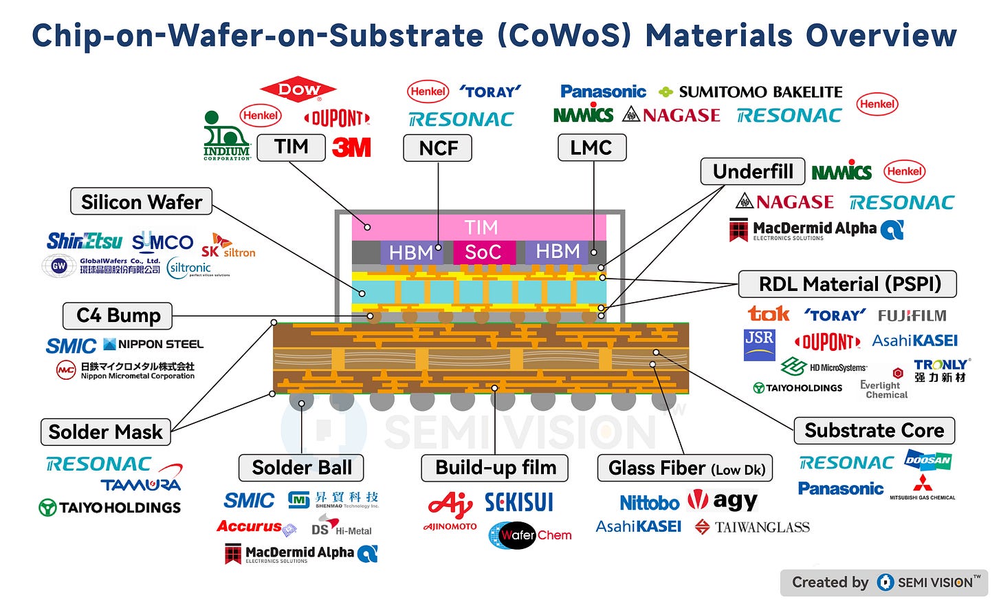
CoWoS is an innovative process, and we have simplified itsprocess flowandsupply chain relationships. Currently, CoWoS requires a wide variety of materials. Taiwan’s supply chain is actively promotinglocal-to-local participation, with suppliers working to qualify materials. However, material qualification involves many factors—such asreliability, reproducibility, and stability—meaning suppliers must patiently navigate a long certification process.
Global Supply Chain Management
The CoWoS supply chain is highly diversified, involvingequipment, materials, and integration, making it one of the mostcomplex manufacturing ecosystemsin semiconductors.
•Challenges: Advanced packaging relies on a highly complex global supply chain. Equipment vendors must navigate trade tensions, tariffs, and logistical disruptions. In addition, raw materials or components sourced from different parts of the world may face shortages or quality control issues, affecting the timely delivery of equipment.
•Opportunities: Diversifying supply sources and investing in regional manufacturing capabilities can mitigate risks. For example, setting up local production and service hubs can help reduce lead times and improve customer support.
Technological Advancements
Positioning and Limitations of CoWoS
The core objective ofCoWoS (Chip-on-Wafer-on-Substrate)is to provide asystem-level integration platformfor AI chips. As AI chip sizes grow rapidly, largesilicon interposersallow logic and HBM memory to be integrated together, deliveringhigher bandwidthandlower latencyperformance advantages.
However, theinterposer areain CoWoS is limited by thereticle size. Currently, TSMC defines9.5X reticle sizeas the threshold. Beyond this limit, conventional CoWoS faces manufacturing bottlenecks.
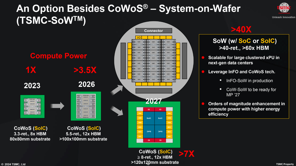
To overcome these challenges, TSMC is promotingtwo alternative paths:
SoW (System on Wafer)– Uses the entire wafer as the platform, breaking the reticle limitation. It is well-suited forultra-large-scale AI system integration.
CoPoS (Chip-on-Panel-on-Substrate)– Provides expansion at the packaging level. While itsperformance densityis not as high as SoW, itscost structure is more favorablethan CoWoS, making it an innovative and scalable compromise solution.
Although CoPoS is relatively cheaper, multiple factors must be considered, including:
Coefficient of Thermal Expansion (CTE) mismatch
Packaging warpage
Power/Signal Integrity (PI/SI)
Substrate manufacturing capability
These challenges make CoPoS acomplex technological innovationthat requirescross-supply chain collaboration.

CoWoS Supply Chain and the Rise of Glass Substrates
TheCoWoS technology chainis primarily concentrated in theCoW (Chip-on-Wafer)segment, where TSMC holds a strong leadership position. As a result, many potential entrants and supply chain partners have chosen to focus on theoS (Wafer-on-Substrate)stage, particularly in advancingnew substrate materials.
This explains why companies inEurope, Singapore, the U.S., and South Koreaare actively investing in:
TGV (Through-Glass Via) processes
Glass Substrates
Glass Interposers
Glass, with itslow dielectric constant (Dk),low coefficient of thermal expansion (CTE), andlarge-area manufacturing advantages, is regarded as a critical material toovercome reticle limitationsand enablehigher signal integrity. This domain is now seen as anew blue ocean for advanced packaging.

Interconnection Density as a Packaging Evaluation Metric
In advanced packaging, one of the most important technical benchmarks isInterconnection Density.
Calculation factors include:
Number of vias or microbumps per unit area (via pitch, microbump pitch)
Number of vertical stacking layers
General observation:
CoWoS + SoICprovides the highest interconnection density available today.
Traditional CoWoS is limited by microbump pitch (~40 μm).
SoIC, with Hybrid Bonding, can shrink pitch to 10 μm or smaller, further enhancing density and signal performance.
SoIC: Capacity and Challenges
Although SoIC’s current production capacity is limited, TSMC is investing heavily in this field.
Its core value lies in enabling direct chip-to-chip bonding viaFace-to-Face (F2F)orFace-to-Back (F2B)methods, which delivers:
Extremely high interconnection density
Lower signal latency
Reduced power consumption
Key challenges include:
Measurement difficulty: Once chips are bonded, probing the electrical and structural state of intermediate dies becomes difficult.
Wafer handling: Thinned wafers are prone to warping and damage.
Reliability analysis: Long-term reliability under thermal cycling, mechanical stress, and bond interface integrity requires rigorous validation.
To address this, the industry is moving towardlow-temperature Hybrid Bonding, reducing thermal stress and material mismatch risks—an area TSMC frequently highlights in its technical papers and international conferences.
Future Applications of Hybrid Bonding
Hybrid Bonding was first applied inCMOS Image Sensors (CIS)for high-resolution pixel stacking.
Looking forward, its applications are expanding:
HBM (High Bandwidth Memory): Direct bonding with logic dies to reduce TSV and microbump limitations.
Optical Engines: Heterogeneous integration of photonic and electronic dies, enabling lower insertion loss and higher energy efficiency.
AI/HPC chips: Ultra-high bandwidth interconnects between multiple dies, scaling next-generation AI accelerators.

2025年7月11日
Tokyo Electron (TEL) has also introduced Hybrid Bonding solutions and highlighted its potential across CIS, HBM, optical engines, and 3D IC—signaling that Hybrid Bonding is becoming aglobal focal pointin advanced packaging.
CoWoS: Key enabler for large-scale AI systems, but limited by reticle size—leading to alternatives like SoW and CoPoS.
Glass substrates and TGV: Emerging as new industry hotspots, driving investment across Europe, the U.S., and Asia.
SoIC + Hybrid Bonding: Offers thehighest interconnection density, though challenged by yield, measurement, and reliability.
Hybrid Bonding’s future: Expanding from CIS to HBM, optical engines, and HPC, positioning itself as thecore technology in packaging evolution.
•Opportunities: Investing in R&D and collaborating with foundries and customers can drive innovation in advanced packaging. Equipment vendors that can provide cutting-edge solutions (e.g., precision assembly, high-throughput bonding, or multi-chip packaging) will be positioned for growth.
Environmental and Sustainability Pressure

- Green Management and Green Manufacturing Strategies
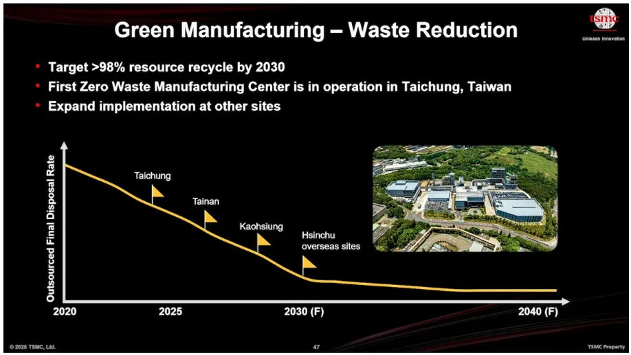
TSMC has fully integrated green management into its daily operations, advancing multiple sustainability initiatives in climate and energy management, water conservation, resource recycling, and air pollution control. The company emphasizes embedding environmental principles into process efficiency improvements and resource savings, striving to become a global benchmark enterprise in environmental protection.
TSMC also continues to introduce energy-saving designs, raw material optimization, and reduction measures into its processes, while actively promoting in-fab resource recycling to enhance resource utilization efficiency.
- Renewable Energy Adoption and RE100 Progress
RE100 Commitment: In 2020, TSMC became the world’s first semiconductor company to join RE100, pledging to power its operations with 100% renewable energy, with the initial target set for 2050.
RE100: An interview with TSMC on its increased ambition
Timeline Acceleration: In September 2023, TSMC announced that its RE100 target had been brought forward from 2050 to 2040. At the same time, the company raised its 2030 renewable energy target from 40% to 60%.
Progress to Date (as of 2024):
All global offices and overseas fabs have achieved 100% renewable energy usage.
Company-wide renewable energy adoption has surpassed 14%.
Supply Chain Collaboration: Through its “GREEN Agreement” with suppliers, TSMC requires domestic suppliers in Taiwan to achieve 85% renewable energy use by 2030, while overseas suppliers must reach 100%. More than 50 suppliers have signed on, covering around 90% of supply chain emissions.
Long-Term Procurement: TSMC pioneered a joint renewable energy procurement model, signing a 20-year power purchase agreement for 20 billion kWh, enabling subsidiaries and suppliers to secure stable renewable electricity sources.
- Carbon Reduction Actions and Targets (Scope 1–3)
Scope 1 (Direct Emissions): TSMC continues upgrading greenhouse gas abatement facilities, adopting carbon-neutral natural gas, and has achieved net-zero emissions for Scope 1 and 2 at overseas sites since 2022. The company has also earned LEED Platinum green building certifications, representing the largest certified floor area in the semiconductor industry.
Scope 2 (Indirect Energy Emissions): In line with its accelerated RE100 roadmap, TSMC is rapidly increasing its renewable energy adoption.
Scope 3 (Value Chain Emissions): Through joint renewable energy procurement, TSMC helps suppliers secure green power, thereby strengthening industry-wide decarbonization capacity.
SBTi Goal: TSMC has pledged to achieve a net-zero target in line with the Science Based Targets initiative (SBTi) by 2035, covering Scopes 1, 2, and 3.

2025年5月17日
TSMC demonstrates a strong environmental commitment by advancing internal energy optimization and emission reduction, while also collaborating with suppliers and pioneering renewable energy procurement. These efforts mark a clear trajectory toward green manufacturing and achieving net-zero goals.
•Challenges: Global environmental regulations, such as those related to energy efficiency, materials usage, and waste reduction, can require equipment vendors to invest in eco-friendly solutions. Balancing sustainability goals with the performance requirements of advanced packaging equipment is a key challenge.
•Opportunities: Emphasizing green technologies, such as energy-efficient packaging and sustainable materials, can appeal to customers seeking to reduce their environmental footprint and comply with regulations.
The TSMC 2023 Sustainability Report covers the Company’s ESG performance over the past year.
Cost and Price Sensitivity in advaced logic node
As the cost of advanced logic processes continues to climb, overallsystem packaging costshave risen sharply. Recent industry surveys indicate that TSMC’s2 nm wafer pricinghas reached$30,000 per wafer, significantly higher than the$18,000–20,000level for 3 nm.
This sharp increase primarily reflects thegreater complexity and expenseof incorporating advancedEUV lithography steps, heterogeneous materials, and GAAFET transistor architectures, which require substantial investment in cutting-edge equipment.
Moreover, the construction cost of a2 nm fabis estimated at$27–28 billion, forcing manufacturers to pass on part of the cost burden to downstream customers.
To address these cost challenges,advanced packaging innovationssuch asCoPoS (Chip-on-Panel-on-Substrate)andCoWoP (Chip-on-Wafer-on-PCB)have emerged.
Challenges:
In a highly competitive semiconductor industry, suppliers face dual pressure toreduce costs while maintaining performance and yield. Packaging equipment vendors must adjust their solutions without sacrificing quality, but soaring front-end manufacturing costs make this task increasingly difficult.
Opportunities:
Vendors capable of offeringhigh-performance, reliable, and cost-efficient packaging solutionswill see stronger demand. Drivingautomation and digitalizationin manufacturing can effectively lower costs, improve yield, and secure a competitive position inprice-sensitive markets.
Customization and Integration
GlobalASIC demandis accelerating, as in-houseCSPs (Cloud Service Providers)aggressively develop their ownAI chips—primarily to undercut the high pricing of NVIDIA’s solutions.
As a result,Broadcom and Marvellhave become critical players in this wave of AI chip development. In earlier sections, we highlighted not only theirASIC business momentum, but also their significant efforts and contributions inoptical interconnect technologies.

2025年2月28日

•Challenges: With the growing trend of application-specific integrated circuits (ASICs) and the need for highly customized solutions, packaging equipment vendors must be flexible and able to meet the unique requirements of different customers.
•Opportunities: Providing tailor-made solutions, along with flexible equipment platforms that can handle various package types and sizes, can set vendors apart in the market. Offering integrated equipment that supports multiple processes, such as testing and inspection, will be a competitive advantage.
Global Competition and Market Consolidation
From Silicon Island to AI Supply Chain
Taiwan, long known as theSilicon Island, is now evolving into acomplete supply chain from AI chips to AI servers. Across upstream, midstream, and downstream segments, the ecosystem operates in full coordination. At present, onlyNVIDIAhas the capability to orchestrate such end-to-end supply chain management—this is why NVIDIA holds thestrongest competitive edge in AI chips.

Meanwhile,Chinais also aggressively developing its AI industry. The country possesses a vast pool of AI talent, but due to the ongoingU.S.–China semiconductor conflict, the importance of domestic chip development has been placed squarely onSMIC, withHuaweiserving as a crucial industry leader. Huawei’sAscend chipshave become a key indicator of China’s progress, showing that it has reached a certain level of capability. At the same time, many Chinese firms are actively entering the self-developed chip market.

2025年3月28日
Yet, a central question remains: under restrictions on access to advanced semiconductor equipment, SMIC has relied onDUV lithographyto develop high-end chips for localization purposes. While China faces difficulties in acquiring tools foradvanced packaging, it continues to push forward with research inHybrid BondingandFOPLPtechnologies. Furthermore, significant resources are being invested intoSilicon Photonicsas part of the country’s long-term strategy.

Turning toSouth Korea, the spotlight is onHBM, whereSK hynixhas emerged as the biggest winner, whileSamsungis still working hard to catch up. In advanced process technology, Samsung has faced hurdles with yield rates and customer demand, but recently secured aTesla order, marking a notable success. On the advanced packaging front, Samsung has introduced its own packaging platform; however, such platforms must still be paired withleading-edge logic processesto deliver real competitiveness. Looking ahead,glass substratesmay provide Samsung with a new strategic pathway.
Tesla-Samsung $16.5 billion supply deal may spur chipmaker's US contract business
Glass technologies—includingglass interposers, glass carriers, and glass substrates—offer diverse applications across packaging and integration. Each, however, requires significantlesson learningbefore reaching maturity.

2025年4月22日
•Opportunities: Strategic partnerships, mergers, or acquisitions with key players in the semiconductor and packaging ecosystems can help vendors strengthen their market position. Expanding into emerging markets where demand for advanced packaging is increasing (e.g., automotive, IoT, and 5G) is another growth opportunity.
Adapting to Customer Needs
In the AI era, TSMC has effectively become the world’s sole and irreplaceable manufacturing supplier for AI chips. Notably, its success does not rely solely on leadership in advanced logic process nodes. As technology continues to scale down, the challenges of CMOS scaling have intensified significantly. While Moore’s Law is slowing, TSMC has still demonstrated meaningful innovation in the transition from N3 → N2, marking a generational leap from FinFET structures to GAA (Gate-All-Around) transistors. This represents a dramatic shift for chip designers. To reduce the burden of “lesson learning” in design migration, TSMC introduced the Transformer Flow, a design conversion tool that enables customers to move efficiently into GAA, underscoring TSMC’s deep strength in Design-Technology Co-Optimization (DTCO).
2025年2月5日
Looking ahead toA16 and A14 nodes, TSMC has adopted adual-track strategy:
A16:ImplementsBSPDN (Backside Power Delivery, SPR solution), a fundamental restructuring of the power delivery network.
A14:Extends theN2 CMOS scalingpath, providing a more conservative option for customers who prefer incremental design migration.
This dual-track approach not only reflectsdifferent customer preferences for risk-performance trade-offs, but also demonstrates TSMC’s flexibility in steering the industry roadmap.

2025年5月9日
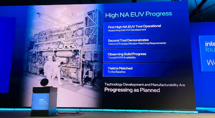
Against this backdrop, comparisons with Intel often arise: Intel is advancing with PowerVia and High-NA EUV, while TSMC has not yet adopted High-NA EUV. How does TSMC remain competitive? The key lies in its vertical integration across design, process, and packaging. By leveraging a mature EUV ecosystem, improving multi-patterning efficiency, and strengthening Advanced Packaging capabilities, TSMC has forged a path distinct from—but equally effective as—Intel’s.
(Image credit: Tom's Hardware)
2025年5月1日
Advanced Packaging and Silicon Photonics Integration
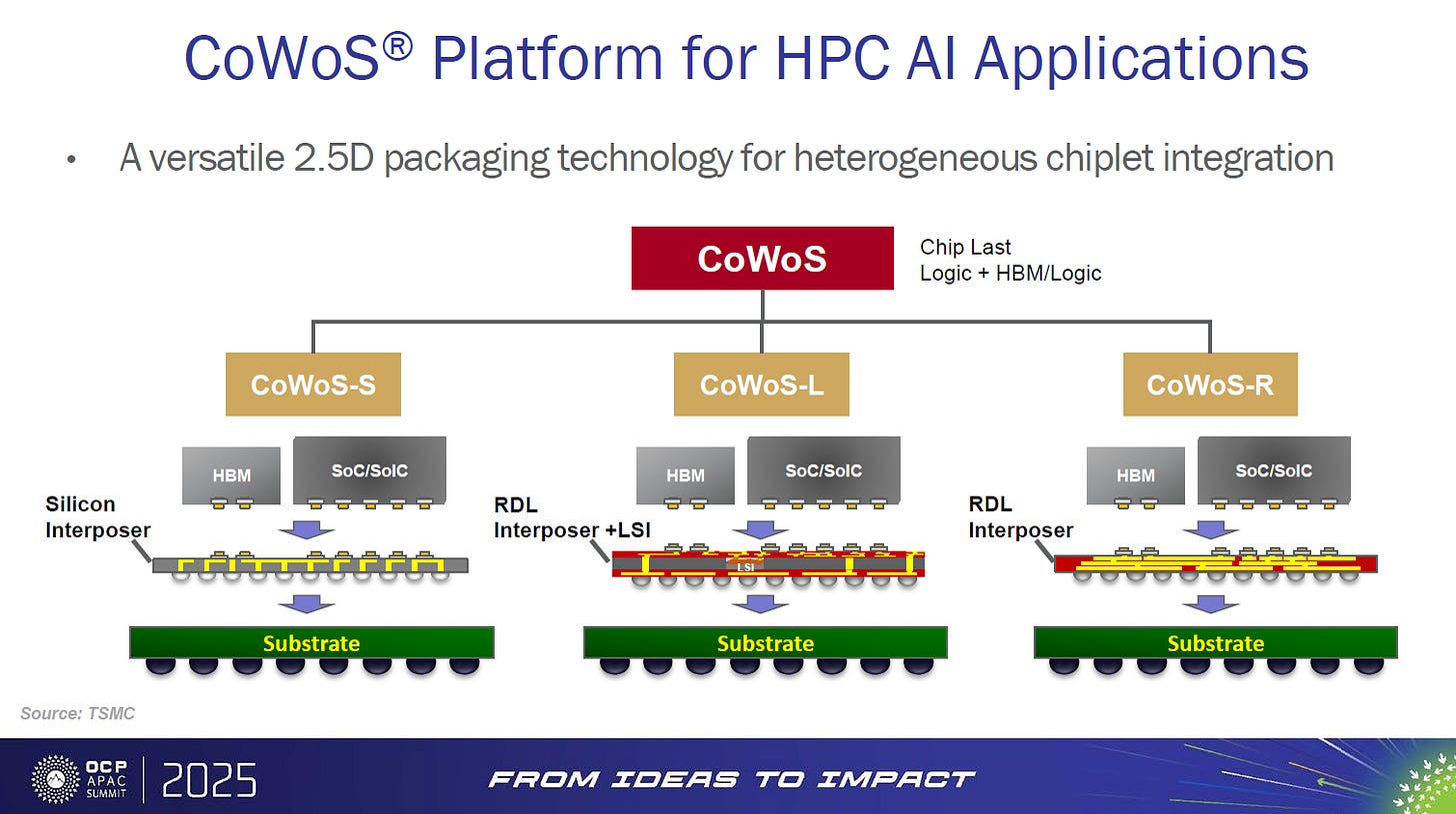
TSMC has long regardedAdvanced PackagingandSilicon Photonicsas thesecond growth curve beyond process scaling. Following the evolution fromCoWoS → SoW (System on Wafer) / CoPoS (Chip-on-Panel-on-Substrate), the next step is clear: strengtheningSoICand3D Stackingto enhancesystem-level interconnection density.
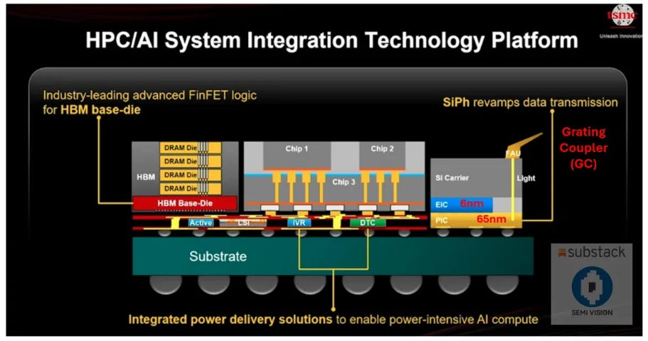
However, as AI chip designs become increasinglylarge and complex, simple logic stacking is no longer sufficient. Challenges inPower Integrity (PI)andSignal Integrity (SI)are emerging rapidly. To support high-speed, large-scale AI computation, TSMC and the industry have proposed multiple device-level solutions:
eDTC (embedded Deep Trench Capacitor):Reduces PDN impedance and enhances power stability.
IVR (Integrated Voltage Regulator):Enables fine-grained on-chip voltage regulation, minimizing transmission loss.
IPD (Integrated Passive Devices), MIM (Metal-Insulator-Metal Capacitor), and MtM (Metal-to-Metal):Improve signal quality and reduce parasitic effects.
How to efficiently integrate these components within advanced packaging has become a central focus for both TSMC and industry R&D. A growing number of technical papers point toward a future centered on System Technology Co-Optimization (STCO).

2025年5月27日
From Copper Interconnects to Optical Interconnects: Materials and Physical Limits
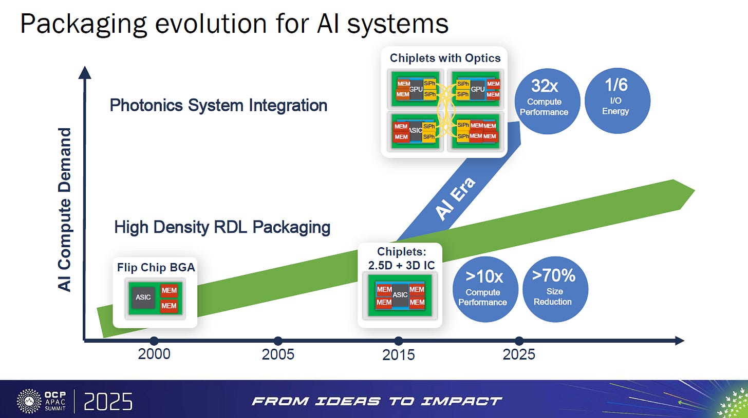
As traditionalcopper interconnectsface fundamental physical limits in bandwidth and power consumption,Optical I/Ohas become the inevitable successor.
The key challenge lies inpractical deployment:
Technology Maturity: A complete solution is required, evolving from optical engines to standardized modules such asCPO (Co-Packaged Optics)andLPO (Linear Pluggable Optics).
Customer Adoption: The pace of deployment will depend heavily on real-world adoption byhyperscalersandAI chipmakers.
Currently, major players are already conducting real-world validation:
NVIDIAhas demonstrated high-performance applications of optical interconnects through itsCPO switch.
BroadcomandMarvellare advancing co-packaged optics integration inEthernetandSerDes.

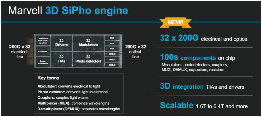
These breakthroughs highlight one overarching reality:silicon itself has inherent limits, making the search for the next-generation“successor to silicon”an urgent priority.
In previous articles,SemiVisionhas discussed extensively the development of silicon photonics technologies by Broadcom and Marvell, while also exploring some questions from a materials perspective. For more details, readers may refer back to those earlier discussions.
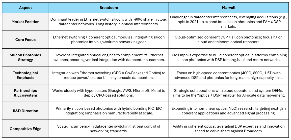
When looking at silicon photonics within TSMC’s published roadmap, we can see certain applications emerging—particularly the integration ofoptical enginesusinghybrid bondingto connect PICs (photonic integrated circuits) with EICs (electronic integrated circuits). However, TSMC’s current focus remains largely onsilicon-based photonics. At the same time, we observe that leading foundries worldwide are moving aggressively into applications involvingnon-linear optics (NLO). These areas are extremely complex, and as such, NLO is becoming an increasingly important topic of research and development.
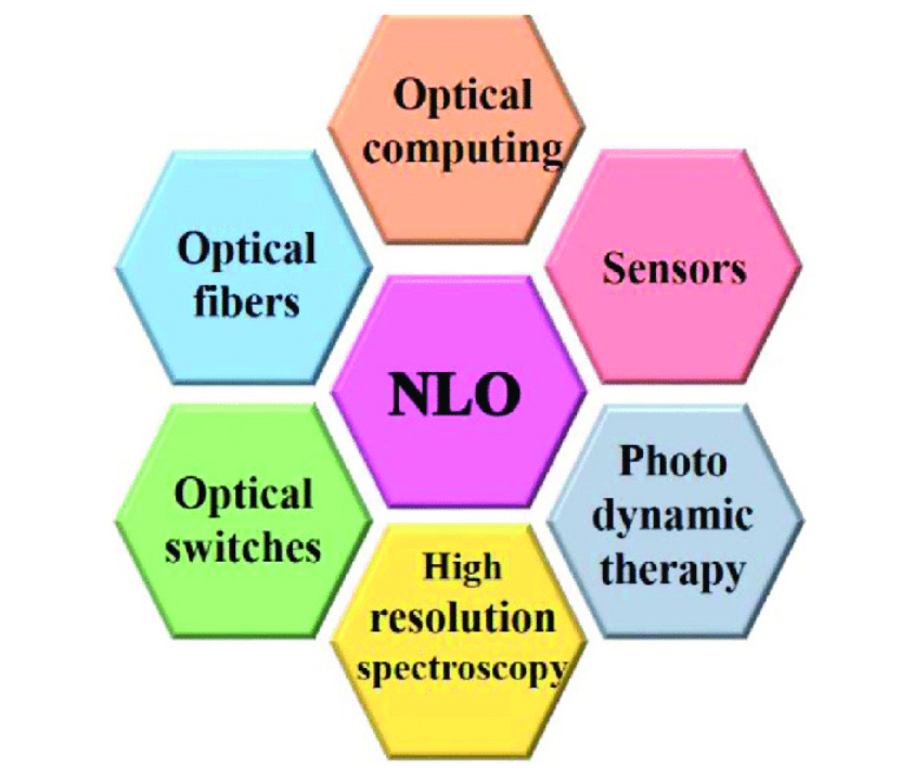
Nonlinear Optics and Material Innovation
Nonlinear optics (NLO) is increasingly regarded as a highly promising option. At its core, it seeks to leverage the properties of new materials to overcome performance bottlenecks in optical transmission and signal modulation. However, since wafer fabs have long relied on silicon-only processes, the introduction of new materials (such as LiNbO₃, III-V compounds, or TFLN) faces significant challenges:
Process integration: Preventing contamination from heterogeneous materials.
Yield control: Ensuring consistency across multi-material processes remains an obstacle.
Cost efficiency: NLO components must achieve a viable cost structure at the system level.
Currently, multiple forums and industry–academia collaborations in Europe, the United States, and China are actively advancing nonlinear optical applications, while the broader industry ecosystem is beginning to explore the potential for cross-material collaboration.
In summary, TSMC now stands at the intersection of three major strategic axes:
Advanced process technologies (N2 → A16/A14):the transition to GAA and BSPDN.
Advanced packaging (SoIC, 3D Stacking):system-level optimization.
Optoelectronic interconnects and materials innovation (CPO, nonlinear optics):next-generation breakthroughs.
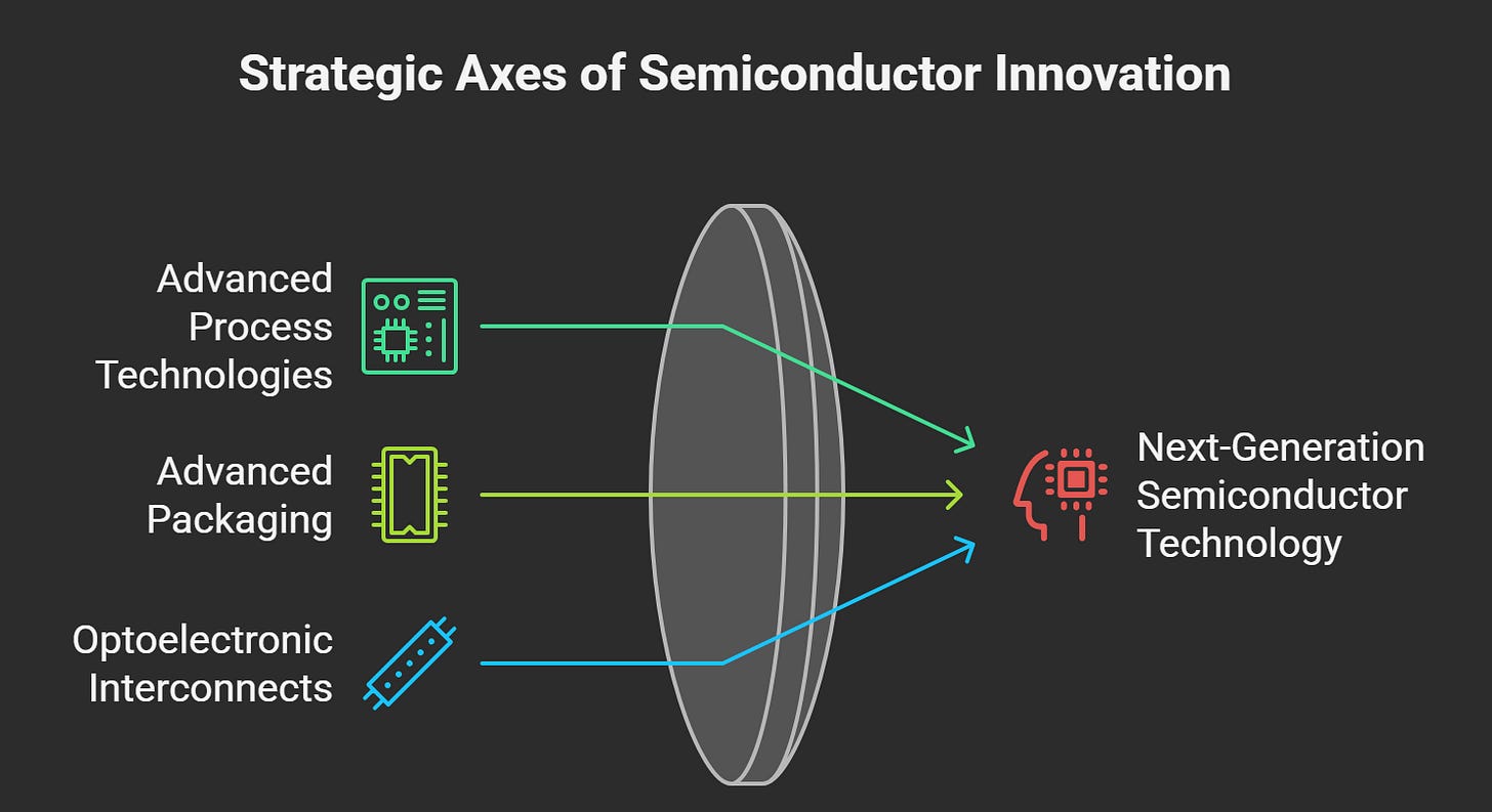
Together, these three directions will determine whether TSMC can maintain its leadership in the AI infrastructure era and will profoundly shape the technological evolution of the global semiconductor industry.
•Challenges: Semiconductor manufacturers are increasingly looking for faster time-to-market and more integrated solutions. Equipment vendors must adapt quickly to the rapidly changing needs of customers in areas like 5G, AI, and automotive electronics.
•Opportunities: By staying close to their customers and understanding their evolving needs, vendors can develop products that are highly aligned with industry trends. This customer-centric approach will build long-term relationships and trust.
In summary, advanced packaging equipment vendors can navigate the globalized landscape by focusing on technological innovation, cost efficiency, sustainability, and customization while adapting to market shifts and customer demands.


PreviousNext
TopLatestDiscussions








See all