Semiconductor IC Testing: A Comprehensive Analysis from Core Processes to Advanced Packaging Challenges
Semiconductor IC Testing: A Comprehensive Analysis from Core Processes to Advanced Packaging Challenges
- Source: SemiVision
- Author: SEMIVISION
- Published: 2025-08-20T13:18:45+08:00
- URL: https://tspasemiconductor.substack.com/p/semiconductor-ic-testing-a-comprehensive Semiconductor IC Testing: A Comprehensive Analysis from Core Processes to Advanced Packaging Challenges


Semiconductor IC Testing: A Comprehensive Analysis from Core Processes to Advanced Packaging Challenges
Original Article by SemiVision Research (TSMC , Nvidia , Advantest , Teredyne , KLA, Onto , Camtek, Nova , FiconTEC ,Chroma, Cohu)

Aug 20, 2025
∙ Paid
Semiconductor IC Testing: From Fundamental Processes to New Challenges in Advanced Packaging and the Silicon Photonics Era

In the past, IC testing in semiconductor development was largely regarded as a standard procedure following fabrication. For traditional logic chips, the testing flow typically involved wafer sort, post-package ATE (Automatic Test Equipment) testing, burn-in, and final product verification. While these steps were complex and time-consuming, they were still considered relatively fundamental tasks aimed at filtering defects and ensuring yield.
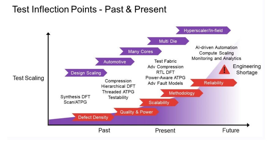
However, with the rise of AI chips, 3D ICs, and heterogeneous integration, testing has evolved into a critical pillar that directly impacts cost, reliability, and co-optimization with design rules. It is increasingly recognized as the next frontier of industry competition.
Source: Synopsys
From Conventional to Advanced Nodes: Coupling Tooling Rule and Packaging Design Rules
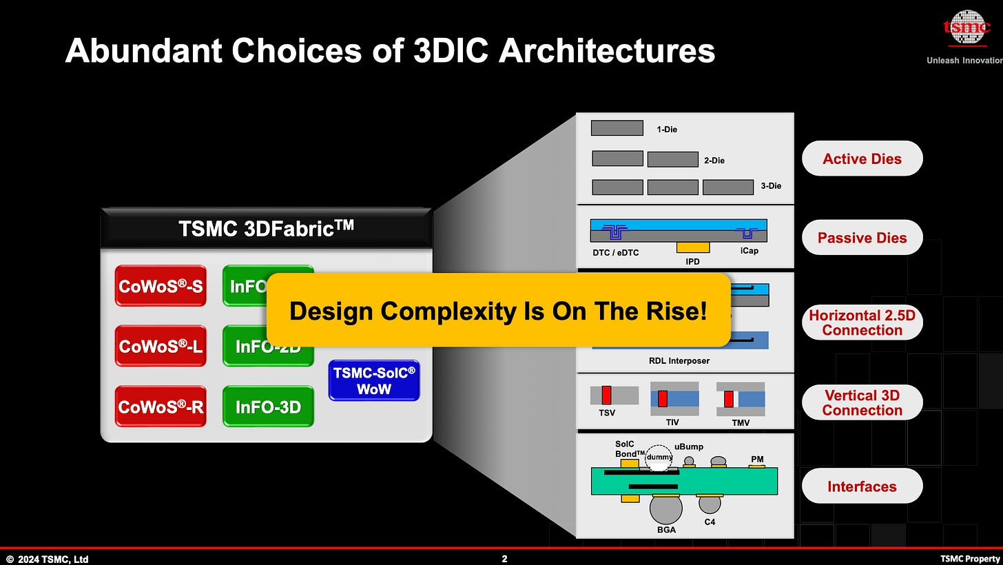
Today, advanced process nodes and advanced packaging are no longer viewed in isolation. When customers evaluate Tooling Rule , they must also consider compatibility with advanced packaging approaches such as 2.5D/3D IC, chiplet, and SoIC architectures. In such system designs, it is not only circuit routing that must comply with design specifications—power distribution networks (PDN), signal integrity (SI), andpower integrity (PI)must also be co-optimized. Otherwise, unpredictable failures may arise under high-speed, high-frequency operation.
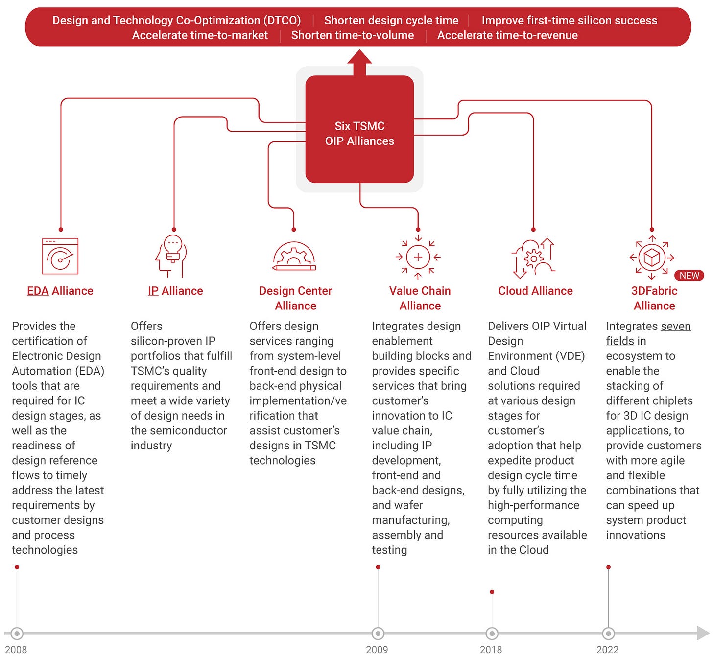
To address this, foundries such asTSMChave introduced dedicated 3D IC design rules, requiring customers’ designs to operate within a defined process window in order to clarify accountability. However, many system companies often prefer to “stretch the rules” in pursuit of maximum performance. This not only tests the flexibility of foundry processes but also elevates the role of testing, making it critical for both early-stage validation and high-volume manufacturing.
Expanding Test Coverage and Reliability Requirements
With rising frequencies and data rates, test coverage has gone far beyond conventional DC tests and functional verification. Greater emphasis is now placed on high-speed interfaces, high-frequency signal integrity, and long-term reliability. For AI chips, which incorporate massive SerDes links, HBM stacked memory, and complex chiplet interconnects, testing methodologies must validate high-speed links, power transients, and cross-die signal transmission.
At the same time, reliability testing requirements have grown significantly, encompassing high-temperature operating life (HTOL), high-voltage stress, thermal cycling, and mechanical stress tests. These measures ensure that products can operate stably over extended lifespans in demanding environments such as data centers and automotive electronics.
The Evolving Roles of ATE, Burn-in, and SLT
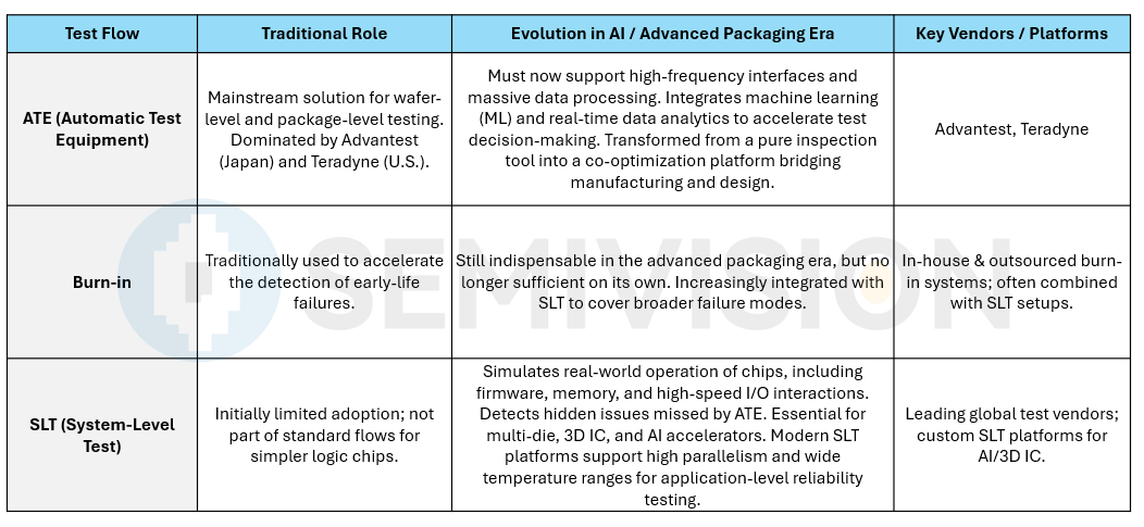
ATE (Automatic Test Equipment): Traditionally the primary solution for wafer-level and package-level testing, dominated by Japan’s Advantest and the U.S.’s Teradyne. With the acceleration of AI chips, ATE must now support high-frequency interfaces and massive data processing, while integrating machine learning (ML) and real-time data analytics to enhance test decision speed. As a result, ATE has transformed from a pure inspection tool into a critical platform for co-optimization between manufacturing and design.
Burn-in: Historically used to accelerate the screening of early-life failures. While still indispensable in the advanced packaging era, Burn-in alone can no longer capture all failure modes and is therefore increasingly integrated with system-level test (SLT).
SLT (System-Level Test): Simulates real-world chip operation, covering interactions among firmware, memory, and high-speed I/O. SLT is capable of identifying latent issues that ATE cannot capture. For multi-die, 3D IC, and AI accelerators, SLT has become an essential stage. Leading global test vendors have introduced SLT platforms that support high parallelism and wide temperature control, bringing reliability testing closer to actual application conditions.
In modern test strategies, a common approach is “Shift Right + Shift Left”: first capture system-level failures through SLT, then feed the failure modes back into ATE and design rules, creating a closed-loop optimization cycle.
Testing supply chain and major suppliers
The semiconductor test supply chain remains dominated by a handful of giants. Japan’s Advantest virtually monopolizes ATE supply for AI and advanced-node chips, whileTeradyneis rapidly expanding in SLT and parallel testing. Supporting equipment such as handlers and probers is largely dominated by Japanese firms such as TEL and Tokyo Seimitsu. This high concentration of the supply chain makes advanced chip testing resources increasingly strategic. Together, Advantest and Teradyne account for more than 70% of the global ATE market.
Chromahas achieved strong penetration and rapid growth in Asian markets, particularly in Taiwan and China.
Cohu(including Xcerra and LTX-Credence) holds a position in the market by offering a comprehensive “ATE + Handler” solution.
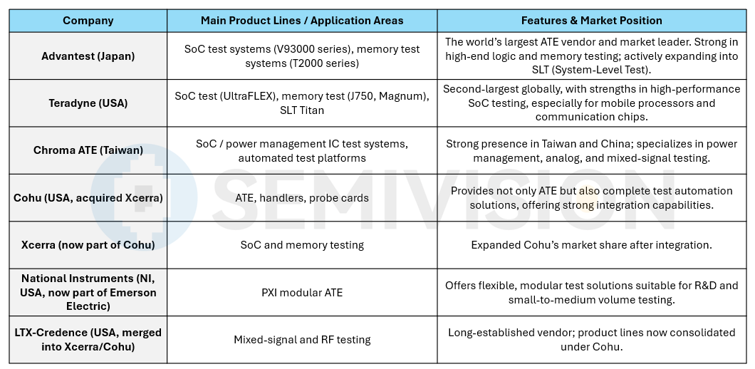
Meanwhile, regional players in China and Southeast Asia are emerging in niche markets such as automotive and consumer IC testing, presenting new competition to the international leaders.
In this article, our focus will be on key challenges in semiconductor testing and an analysis of testing methodologies. We will also provide a basic overview of the upstream, midstream, and downstream segments of the supply chain.
In semiconductor manufacturing, Wafer Acceptance Test (WAT) and Process Control Monitor (PCM) are critical quality checkpoints conducted after wafer fabrication. By measuring multiple monitoring structures, they evaluate both across-wafer and intra-wafer electrical distributions, providing customers with essential data to assess process uniformity and yield. At the same time, fabs also perform QA defect density inspections to ensure products meet specifications before proceeding to subsequent processes or shipment. Traditionally, this stage marked the “end point” of a foundry’s responsibility. However, with the rise of advanced packaging, it has increasingly evolved into the “starting point” of the packaging process.
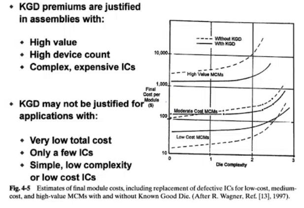
Before entering advanced packaging technologies such as CoWoS, SoIC, or InFO, Known-Good-Die (KGD) screening is mandatory to prevent defective dies from being stacked, which would otherwise result in costly rework. At the same time, the industry has placed greater emphasis on testing interposers and substrates, including RDL formation quality, micro-bump coplanarity, and defect detection. These checks must be implemented at mid-process stages through AOI and electrical testing to avoid defects propagating into final assemblies. Therefore, the true “starting point” of advanced packaging is not only KGD but also yield assurance for interposers and substrates, ensuring stability in subsequent integration.
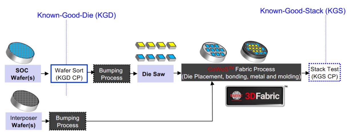
At the CoWoS/SoIC packaging stage, testing focuses on the electrical and reliability characteristics of RDL traces, TSVs, and micro-bumps. Test structures such as daisy-chain, Kelvin, via-chain, and meander patterns are used to validate continuity and RC characteristics, while reliability is assessed under accelerated stress conditions like thermal cycling and baking. Micro-bumps, in particular, require close attention to Joule heating under high current density and coplanarity issues, which are common failure sources. With increasing packaging density and a surge in interconnect counts, both test complexity and cost are escalating significantly.
With the introduction of silicon photonics and co-packaged optics (OIO/CPO), testing challenges rise further. Optoelectronic integrated components must undergo not only electrical testing but also optical characterization, including insertion loss, extinction ratio, coupling efficiency, and electrical parameters such as BER, eye diagrams, and aging performance. This demands test platforms capable of supporting optical fixtures, precision alignment processes, and system-level correlation testing for thermal drift and long-term aging. Measurement uncertainty must also be incorporated into guardbands to avoid misjudgments. These requirements highlight why traditional logic testing methodologies are no longer sufficient to meet future demands.
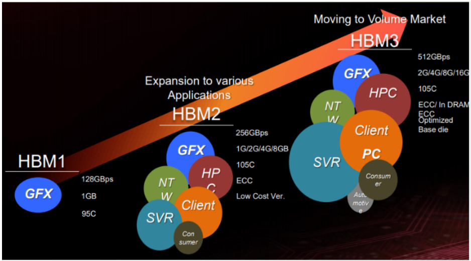
In GPU and HBM high-bandwidth integration, signal integrity (SI) and power integrity (PI) have become critical factors for system-level optimization. By strengthening the power delivery network (PDN), increasing metal thickness, and adopting advanced RDL designs (such as eDTC technology), jitter and power consumption in high-speed data transmission can be effectively reduced. The linewidth, spacing, and layout of RDL have significant impact on SI/PI, requiring close coordination across design, packaging, and testing stages.
Meanwhile, the acceleration of SerDes and PCIe introduces new challenges. For example, in PCIe 7.0, operating at 32 GHz, channel loss, jitter, and BER specifications are far more stringent. To meet these requirements for high-speed serial links, server motherboards must employ ultra-low Dk/Df materials such as Megtron 7 or Tachyon. This means that testing must extend beyond IC-level validation and be closely integrated with PCB material choices and system design, forming an end-to-end testing methodology.
In summary, the role of testing has evolved from being the “end point of wafer-level inspection” to the “starting point of advanced packaging,” and is now progressing toward the “core of system design and packaging integration.” This progression spans wafer-level WAT/PCM and QA, KGD and interposer screening, CoWoS/SoIC packaging tests, silicon photonics and optoelectronic integration, as well as system-level validation of GPU × HBM and SerDes/PCIe. By strengthening interposer screening and optical-electrical measurement planning, this holistic testing framework can serve as an internal standard, enabling designers, foundries, OSATs, and testing teams to collaborate effectively and ensure quality and reliability from process to system.
SemiVisionhas conducted an in-depth analysis of the current inspection and testing supply chain, covering key suppliers in Inline Inspection. Leading players include KLA (optical and e-beam inspection and metrology platforms), Onto Innovation (optical defect inspection, overlay, and metrology solutions), Camtek (wafer AOI and automated packaging inspection), Nova (optical metrology and material characterization), and Hitachi High-Tech (SEM and metrology equipment). Together, these companies form a comprehensive ecosystem for inspection and metrology across different stages of wafer process control and defect detection.

2025年4月15日

2025年8月10日
2025年7月16日
Source: Synopsys
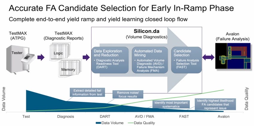
In the areas ofFailure Analysis(FA),Material Analysis(MA), andReliability Analysis(RA), the article also introduces widely used techniques. For example, TEM (Transmission Electron Microscopy) is used for nanoscale lattice and defect observation; SEM (Scanning Electron Microscopy) is applied for surface morphology and cross-sectional structure analysis; FIB (Focused Ion Beam) enables precision cross-section preparation and circuit modification; and SIMS (Secondary Ion Mass Spectrometry) allows depth profiling and dopant concentration analysis. For advanced packaging, Acoustic Microscopy is used to detect voids and delamination inside packages, while TSV and 3D IC structures often require X-ray and CT (Computed Tomography) for observing buried structures and interconnect integrity.
The article further extends to new challenges in silicon photonics and optoelectronic testing, including the measurement of optical parameters such as insertion loss, extinction ratio, and coupling efficiency, as well as high-speed driver and TIA eye diagram and BER testing. It emphasizes that traditional logic testing methodologies are insufficient for the demands of photonic-electronic integration. Finally, SemiVision also reviews foundational testing concepts—from CP (chip probe/wafer test), FT (final test), to SLT (system-level test)—along with the introduction of modern testing strategies such as Part Average Testing (PAT) and Adaptive Test (AT), providing readers with a complete view of the semiconductor testing and inspection ecosystem.
This article will serve as a must-read reference for anyone seeking to understand the full chain from wafer processing and packaging to system-level testing. Whether the focus is on the equipment supply chain for industry analysis or the technical depth needed by engineers, readers will find substantial value.
SemiVisionhas pointed out that future design will move toward chiplet architectures, which means the complexity in testing will only continue to increase. SemiVision recommends that readers who are interested in chiplets consider attending this seminar.
NHanced Semiconductors & University of Florida to Present Chiplet Paper at 36th Electronics Packaging Symposium Held at GE’s Aerospace Research Campus
NISKAYUNA, NY (August 19, 2025) – At the upcoming 36thElectronics Packaging Symposium, held September 3 – 4, 2025, NHanced Semiconductors and a team from the University of Florida will present a technical paper – “The Future of Electronics Packaging: Chiplet Architecture and AI Defect Inspection” – describing how copper-to-copper hybrid bonding enables chiplet interfaces at sub-10µm pitches to increase interconnect densities in advanced packaging assemblies.
NHanced vice-president Dr. Charles Woychik will present the paper, co-authored with U F’s Pavanbabu Arjunamahanthi, et al. from the Department of Electrical & Computer Engineering, during the Symposium’s session on Heterogeneous Integration.
The paper examines the emerging chiplet ecosystem including process architectures, integration flow, and fabrication challenges associated with hybrid bonding for chiplet-to-wafer packaging. Also included are standardization trends, such as Universal Chiplet Interconnect Express (UCIe), that guide the development of scalable, high-yield chiplet integration platforms.
According to Woychik, “Hybrid bonding has emerged as a leading solution for fine-pitch die-to-die chiplet integration with robust electrical, mechanical, and thermal continuity. These characteristics are particularly beneficial in chiplet architectures for high performance computing.”
The36thAnnual Electronics Packaging Symposiumwill be held at the GE Aerospace Research Center in Niskayuna, NY from September 3 - 4, 2025. The conference is organized by theUniversity of Binghamton’s Integrated Electronics Engineering CenterandThe Center for Advanced Microelectronics Manufacturing, in conjunction with GE Aerospace and IBM Research. The Symposium is focused on electronic packaging and the evolution of advanced packaging toward a chiplet future. Registration for the event is availablehere.
About NHanced Semiconductors, Inc.
Based in the US,NHanced Semiconductorsis the world’s first pure-play advanced packaging foundry, specializing in leading-edge BEoL semiconductor technologies. Its capabilities include chiplets, 3D-ICs, silicon interposers, 2.5D, additive silicon manufacturing, photonics, microfluidics, and other innovative technologies. The foundry works with both standard and non-standard substrates, III‑V compound semiconductors, and many specialized materials.
Headquartered in Illinois, NHanced has a development and manufacturing facility near Research Triangle Park, NC, performing small volume manufacturing, in-house process development, and customer prototyping, and an advanced packaging and assembly facility in Odon, IN. For more information, please visit:
Media contact:
Chris Burke, BtB Marketing Communications
(919) 637-3510
For Paid Members, SemiVision will discuss topics on
Integration Challenges in Future Silicon Photonics Testing
Exploring in Supply Chain (KLA ,Onto ,Camtek ,Nova….)
Supply Chain Dimensions and Collaboration Workflow
Industry Value Chain and Company Types
Key Stages and Objectives of IC Testing: Step-by-Step Screening from Wafer to System
Wafer Acceptance Test (WAT)
Wafer Probe (CP)
Final Test (FT)
Reliability Testing (R-Test)
Electrical Quality Check (EQC)
System-Level Test (SLT)
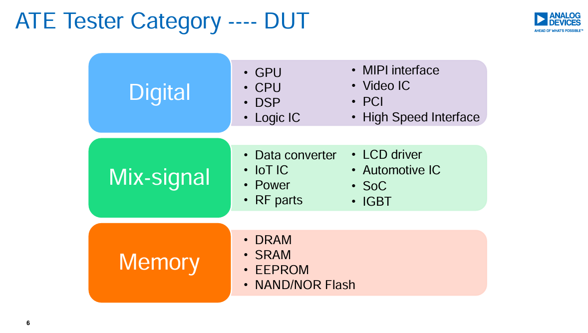
Core Test Technologies and Equipment: Bringing ATE Capabilities “Onto” the DUT
Test Specifications and Datasheet Alignment: One Unified Ruler from Design to Production
Common Test Items: Practical Highlights in DC / Functional / AC
DFT and Memory Testing: Designing Testability In
Boundary Scan and High-Speed Interface Testing
Advanced Packaging (CoWoS / SoIC): Dedicated Test Challenges and Countermeasures
Power Semiconductor Testing: High-Voltage/High-Current Measurements and Reliability
Yield Analysis and Data Science: From Patterns to Root Cause
Test Economics and Capacity Operations: Making Every Second Count
ESD/EOS, Power Sequencing, and Failure Prevention: Testing Is Not a Destructive Experiment
Practical Integration of Advanced Packaging: Design—DFT—Packaging—Testing as One
Integration Challenges in Future Silicon Photonics Testing
As silicon photonics gradually enters HPC and data center applications, testing becomes increasingly complex. Electro-optical integrated chips (EIC + PIC) require not only electrical testing but also optical parameter verification. This means that future test platforms must integrate testers, handlers, wafer probers, and optical measurement modules in order to simultaneously validate high-speed electrical signals and optical performance.
This integration concept will be a key driver in upgrading the supply chain. For example, under the CPO (Co-Packaged Optics) architecture, ensuring coupling yield, insertion loss, and BER performance between the optical engine and ASIC will be core challenges that the testing stage must address.

Semiconductor IC testing is shifting from “passive inspection” to a core function of “design–process co-optimization.” From ATE and Burn-in to SLT, and eventually to silicon photonics testing, the entire supply chain is confronting a new wave of integration challenges. With the advent of the AI and silicon photonics era, testing is no longer merely a yield safeguard—it has become a strategic tool that drives the co-evolution of process, design, and packaging.
In the semiconductor value chain, IC testing assumes the mission of quality verification following design, wafer fabrication, and packaging. As process nodes advance to A16, A14, and beyond—and as 2.5D/3D heterogeneous integration (CoWoS, SoIC) becomes mainstream—testing is no longer just an “acceptance” step. Instead, it spans across design, manufacturing, packaging, reliability, and system integration, forming a closed loop. The rising difficulty and cost of testing make it imperative to strike an optimal balance among test coverage, yield, schedule, and cost—directly impacting both product competitiveness and business performance.
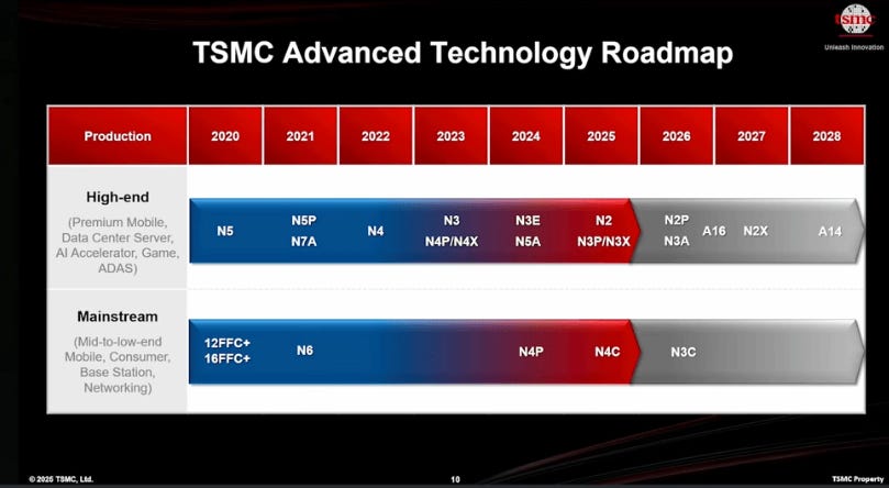
In recent years, CMOS scaling has converged toward two primary vectors:Super Power Rail(SPR, backside power delivery) and Gate-All-Around (GAA). SPR relocates the power network to the wafer backside, alleviating front-side metal congestion and improving IR drop and transient power stability. GAA, by employing an all-around gate structure, enhances electrostatic control, suppresses short-channel effects, and delivers higher device performance. While these innovations do not radically alter the fundamental structure of the upstream material, midstream equipment, or downstream packaging ecosystem—which largely continues under existingPlans of Record (POR)—the industry has begun evaluatingHigh-NA EUVlithography for critical layers. Its single-exposure capability could reduce overlay errors and random defects caused by multi-patterning, thereby offering yield and cost advantages at future nodes.
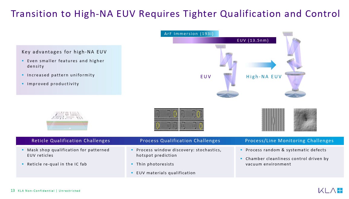
Against this backdrop, the role of testing and metrology is becoming increasingly vital. With SPR and GAA adoption,WAT/PCMmust incorporate backside alignment measurements, residual silicon thickness and wafer warpage control, backside via resistance chains, backside metal electromigration stress tests, as well as Vt variability and self-heating monitoring for GAA devices. High-NA EUV requires additional focus beyond traditionalprocess windows (DoF/E.E.), such as on LER/LWR (line-edge/line-width roughness) and the statistical distribution of stochastic defects. These must be correlated through sensitive test structures, defect maps, and electrical validation to build accurate models. By coordinating across upstream, midstream, and downstream ecosystems—including metrology tools, probe cards, and failure analysis—industry players can establish a complete closed-loop monitoring system, spanning from wafer-level testing to system-level validation. This framework will be essential to ensure yield ramp, maintain performance metrics during advanced node transitions, and pave the way for the cost-effective adoption of High-NA EUV at future technology generations.

In the field of advanced logic processes, the leading inspection equipment suppliers remain KLA, Onto Innovation, Camtek, and Nova, which hold strong advantages in critical dimension (CD) control, line width metrology, defect inspection, and hybrid optical/e-beam measurement. As the industry moves into the GAA, EUV, and high-density interconnect era, their tools have become standard equipment for ensuring yield.
In advanced packaging, however, inspection extends beyond traditional AOI (Automated Optical Inspection), CD, and overlay metrology, requiring more specialized approaches. Examples include:
Acoustic/Ultrasound Inspection: Used to detect voids and delamination in molding film or underfill.
TSV Metrology: Covers 2D/3D mapping, aspect ratio control, via diameter uniformity, and metal fill completeness. In addition to conventional optical metrology, X-ray CT and confocal microscopy are often required for supplementary analysis.
Image Processing & Algorithms: AI/ML-based defect classification to improve anomaly detection rates and traceability in packaging.
For failure analysis and materials characterization, higher-resolution and multi-dimensional tools are relied upon, including:
SEM / TEM: Nanoscale structural and defect observation.
FIB: Cross-section cutting and precision site-specific analysis.
AFM: Surface roughness and nanoscale morphology measurements.
SIMS: Elemental distribution and dopant concentration profiling.
X-ray / CT: Non-destructive internal structure and packaging defect inspection.
Raman Spectroscopy: Stress distribution analysis and material composition variation monitoring.
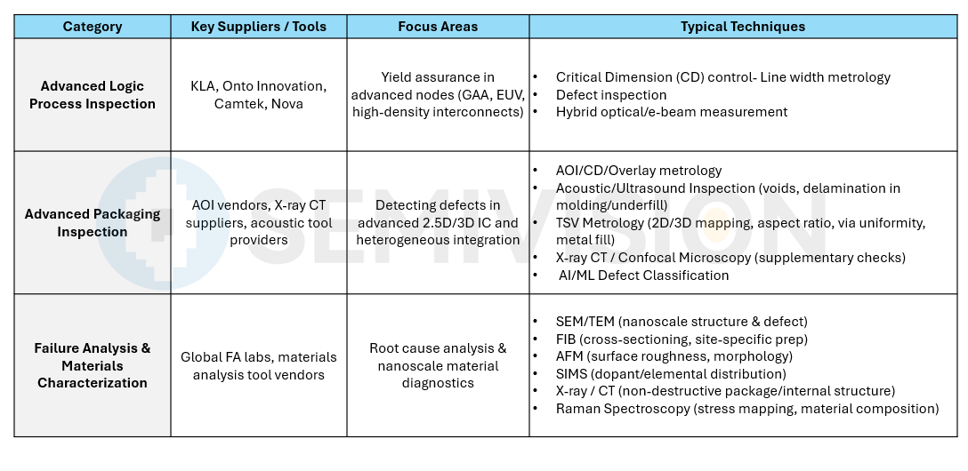
Exploring in Supply Chain (KLA ,Onto ,Camtek ,Nova)
Equipment Layer:KLA, Onto Innovation, Camtek, and Nova occupy central positions in logic process inspection; in packaging, additional specialized suppliers such as Bruker (white light interferometry/AFM), Nordson (acoustic/X-ray), and Hitachi (SEM/TEM) play important roles.
Materials / Process Layer:Collaboration with wafer foundries such as TSMC, Samsung, and Intel, as well as OSAT providers like ASE, Amkor, and SPIL, is essential to ensure that packaging materials (molding compounds, RDL, TSV) are properly matched with inspection solutions.
Back-End Validation / FA Laboratories:Reliability labs of companies such as ASE and TSMC, along with equipment vendors like Keysight and JEOL, provide failure analysis and reliability measurement capabilities.
Through this vertical integration of inspection and analysis across the supply chain, yield optimization in advanced process nodes and advanced packaging can be achieved, forming a closed loop of Design → Process → Inspection → Analysis → Feedback. This closed-loop system is becoming a key enabler for the semiconductor industry to advance toward next-generation nodes.

Major Equipment Suppliers
KLAprovides comprehensive defect inspection and metrology tools for Advanced Wafer-Level Packaging (AWLP), including:
Kronos 1190: High-resolution optical defect inspection system, suitable for Cu-pillars, Cu bumps, TSV, and RDL. Capable of identifying 150 nm-level defects and supporting process monitoring.
CIRCL-AP: Modular cluster platform covering defect inspection and metrology across 2.5D/3D advanced packaging flows.
PWG5™ XT: Detects wafer shape and large voids after bonding, enhancing pre- and post-bond key control monitoring.
Zeta™-5xx/6xx: Automated optical profilometry system for bump height, RDL CD, UBM step height, film thickness, wafer bow, and other parameters.

Onto Innovationoffers key tools widely used in advanced packaging, such as:
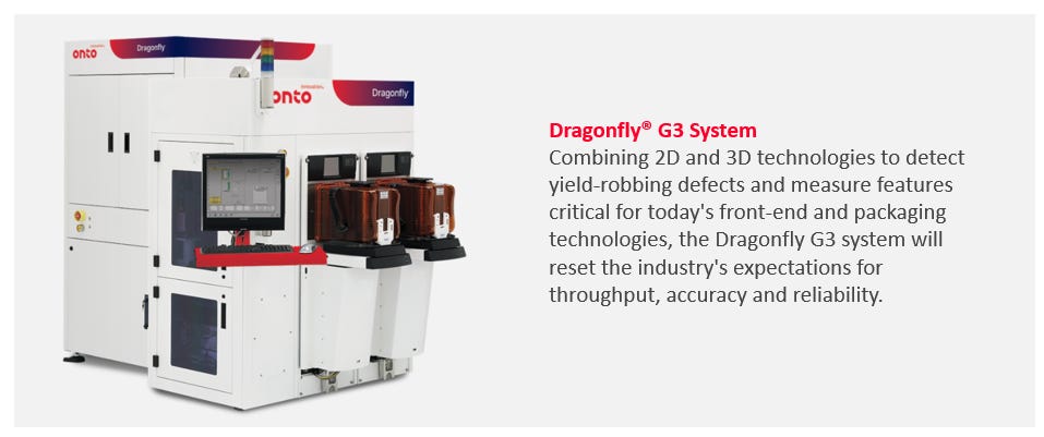
Firefly G3: Supports 2D/3D defect inspection and metrology, including bumps and packaging defects.
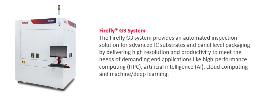
NSX® / F30®: Comprehensive platform for CD, RDL/TSV, 2D bump, and full 2D/3D surface measurements.
Echo™ (Opto-Acoustic): Acoustic-based thin-film metrology tool, capable of detecting voids that may form within molding compounds.
Other tools: Firefly (submicron panel inspection), IVS series (overlay/CD/height metrology), Atlas V (thin film/OCD), Element (FTIR spectroscopy), Aspect (high-aspect-ratio OCM).
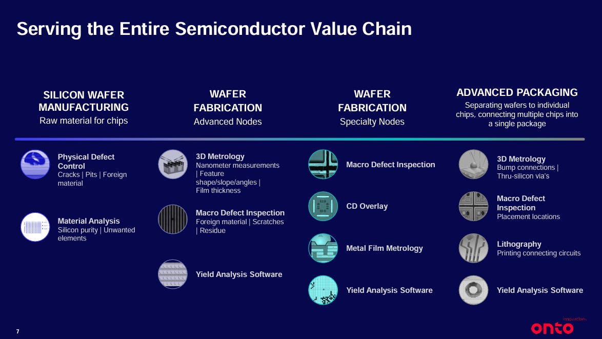
Other Suppliers:
Bruker, Camtek, and Nova also provide a wide variety of optical/electronic inspection and metrology solutions.
Bruker’swhite light interferometry (WLI)tools enable high-precision measurement of bump height variation, die shift, and other surface parameters.
While WLI cannot detect voids (as light cannot penetrate), it is often combined with X-ray and other non-destructive testing techniques to achieve comprehensive coverage.

Specialized Inspection Methods in Packaging Processes
Ultrasound / Acoustic Inspection (Opto-Acoustic):
For example, Onto’s Echo™ can measure voids within molding films using a non-contact acoustic approach.
2D / 3D Mapping and Imaging Techniques:
Optical metrology is used to capture the 3D structure of RDL/TSV, enabling analysis of CD, height, and morphology.
Systems such as Dragonfly G3 and NSX perform full-surface 2D/3D scanning and defect mapping.
Confovis offers AOI and multi-sensor metrology for 3D stacked chips (3D IC), providing precise evaluation of CD, topography, and layer stack.
Non-Destructive Materials Analysis / Failure Analysis Tools:
Includes TEM, SEM, FIB, AFM, SIMS, X-ray, and Raman for high-resolution destructive or non-destructive analysis.
X-ray combined with AI can be applied in advanced packaging to perform 3D measurement and detection of buried interconnects (e.g., voids and defects).
Comet Yxlon: High-End Industrial X-Ray & CT Solutions
Comet Yxlon is a global leader in industrial X‑ray and computed tomography (CT) systems, providing non-destructive testing (NDT) solutions across a wide range of industries—from R&D labs to high-volume production environments
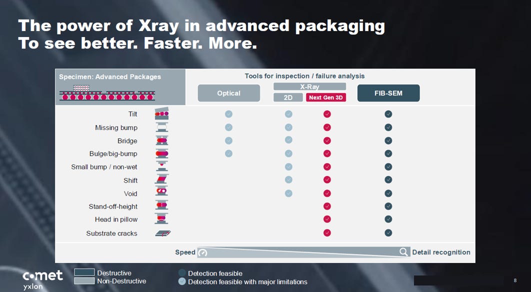
Technologies & Software Capabilities
Industrial X‑ray & CT Technologies
Comet Yxlon’s systems cover a broad energy range (20 kV–600 kV) and support various NDT scenarios—from small components in semiconductors to bulky aerospace parts.
Computed Laminography
A specialized technique for inspecting flat or non-rotatable components (e.g., PCBs or 3D stacked chips), providing faster and more efficient imaging than standard CT.
Geminy Software Suite
A unified user interface supporting CT workflows with automation features, artifact reduction, and advanced CT techniques for consistent, reliable inspection results.
Data Analytics & AI Integration
Comet Yxlon integrates AI-powered tools such as:
Dose Manager to protect sensitive components during inspection.
Batch Manager for seamless multi-part processing.
Dragonfly 3D World for intuitive 3D image analysis and deep learning segmentation of scan data
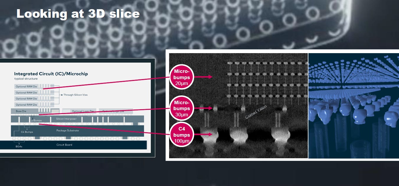
Supply Chain Dimensions and Collaboration Workflow
Positioning of Equipment Suppliers
KLAandOnto Innovationare the mainstream suppliers. KLA is strong in modular cluster platforms and AI-enabled toolchains, while Onto excels in diverse panel/molding metrology and acoustic defect inspection.
Camtek,Nova, andBrukerprovide complementary solutions, particularly for optical/e-beam inspection addressing specialized needs.
Confovis, as an emerging AOI supplier for 3DIC, is well-suited for customers requiring high-precision heterogeneous integration.
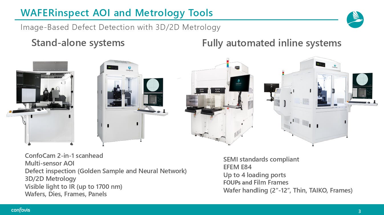
Confovis Technology Overview
Confovis specializes in optical inspection and 3D surface metrology. Its patented CONFOCAM module combines confocal microscopy with optical sectioning, making it suitable for inspection across semiconductors, advanced packaging, glass, metals, and polymers.
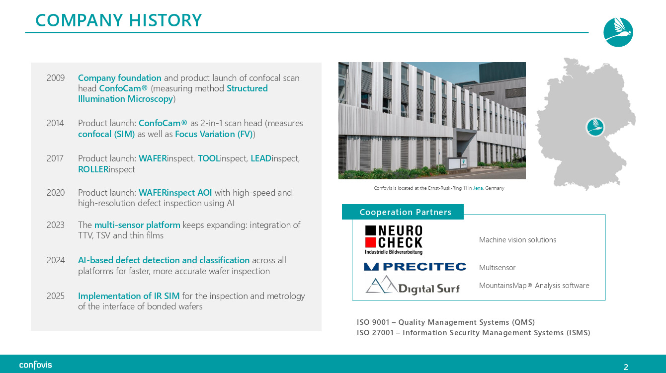
Key Technical Features
Material-Independent
Performs consistently across metals, glass, semiconductors, and polymers.
AOI with RGB & High-NA Lenses
Equipped with high numerical aperture lenses and RGB imaging, enabling high-contrast images and optimized illumination for improved automated optical inspection (AOI).
Large Field of View
Covers wider areas in less time without compromising resolution, improving inspection efficiency.
Surface & Sub-Surface Defect Detection
Capable of detecting both surface and sub-surface defects. Using SIM (Structured Illumination Microscopy), the system provides optical sectioning for in-depth inspection of RDL, TSV, and 3DIC stacks.
Best-in-Class Components
Built with industrial-grade optics and mechanical parts to ensure system stability and long-term reliability.
Application Areas
Advanced Packaging: CD/overlay and defect inspection for RDL, TSV, and micro-bumps.
3DIC Stacking: Inspection of layer alignment, warpage, and structural integrity of stacked dies.
Material Inspection: Surface and sub-surface defect detection in glass, polymers, and metals.
AI/Automated Inspection: Integrated algorithms for defect classification to enhance efficiency in high-volume packaging inspection.

Upstream Process Integration
Close coordination with equipment vendors is required during process steps, for example:
During wafer thinning and bonding, tools like PWG5 XT are used for shape and void monitoring.

For RDL/TSV lithography, overlay, and CD control, platforms such as Dragonfly, NSX, and IVS are deployed in parallel.
After molding, thin-film void and film stack inspection is performed using acoustic systems like Echo or X-ray tools.
Failure Analysis and Quality Feedback
When abnormalities are found at a fab or OSAT, root cause analysis can be conducted using SEM, TEM, FIB, AFM, SIMS, and Raman.
Coupled with AI/ML-based analytics (e.g., X-ray + ML), defect recognition models and process feedback mechanisms can be established.

Key Suppliers
KLA, Onto Innovation, Camtek, Bruker, Nova, Confovis
Optical Metrology Tools
Acoustic Inspection (Void Detection)
3D / TSV / CD Mapping
Non-Destructive Inspection (X-ray / AI)
X-ray + ML for non-destructive buried interconnect analysis
Destructive Failure Analysis Tools
TEM, SEM, FIB, AFM, SIMS, Raman
Supply Chain Integration Approach
Process integration with tools, failure analysis feedback, and the adoption of AI-driven data analytics.
Industry Value Chain and Company Types
The semiconductor industry value chain can be broadly divided into three main stages: upstream IC design, midstream wafer fabrication (foundry), and downstream packaging and testing (OSAT), before ultimately moving into distribution and system integration. Depending on their business model, companies vary in how much control they have over testing:

Integrated Device Manufacturers (IDMs) – Companies such as Intel and Samsung manage design, fabrication, packaging, and testing in-house. Their test strategies can be deeply co-optimized with process and packaging, but this model comes with the highest capital and technology barriers.
Fabless Companies – Firms such as NVIDIA, Apple, and MediaTek focus solely on design, while manufacturing and packaging/testing are outsourced to foundries and OSAT providers. This model requires tight collaboration among design companies, foundries, and OSATs to share design-for-test (DFT) features and yield improvement mechanisms.
IP Design Service Companies – Providers like ARM and M31 supply semiconductor IP and test controllers (e.g., MBIST controllers, boundary scan circuits), helping customers shorten the time needed to integrate and deploy testing.
OSAT (Outsourced Semiconductor Assembly and Test) Providers – Deliver end-to-end services such as wafer probing, packaging, final test, and system-level test. According to TrendForce’s 2024 survey, the global top 10 OSAT companies by market share are ASE Group, Amkor Technology, JCET, Tongfu Microelectronics, Powertech Technology (PTI), Huatian Technology, China Testing International, Hana Micron, KYEC, and ChipMOS. Notably, Chinese firms such as JCET and Huatian Technology have grown rapidly in recent years.

Key Stages and Objectives of IC Testing: Step-by-Step Screening from Wafer to System
Wafer Acceptance Test (WAT)
Wafer Acceptance Test (WAT) represents the earliest stage of mass production testing and serves as the closest electrical health check to process physics. Using standardized test keys (PCM/test keys), WAT measures parameters such as threshold voltage (Vt), drive current (Idsat), subthreshold slope, gate leakage, sheet resistance, contact resistance, metal RC delay, dielectric reliability, and E-test ring oscillators. These results establish statistical baselines at the wafer, lot, and tool levels.

WAT structures are typically located in the scribe line or around the die periphery, sharing the same process history as the product. This makes them effective indicators of within-wafer (WiW) uniformity, wafer-to-wafer (WfW) variation, and across-tool differences. Engineers apply SPC/Xbar-R charts, box plots, and interquartile range (IQR) limits, combined with Western Electric / AIAG rules, to detect process shifts and drifts. When Cpk weakens or means deviate, process modules such as ion implantation, annealing, etching, metallization, and CMP are traced for recipe and target review.
Compared to inline metrology (e.g., CD-SEM, film thickness, stress, resistivity), WAT provides more direct linkage to device models. It supports PVT corner extraction, SPICE calibration, LEGO parameter modeling, and yield attribution, and it connects with design guard-bands to provide dynamic limit-setting for downstream tests. For high-current and high-density interconnect generations, Kelvin structures and via-chains reveal open/short defects, voids, and electromigration vulnerabilities early. At advanced nodes, additional monitors such as layout-dependent effect (LDE) sensors, thermal diodes, and power network IR-drop probes are included, linking device testability to product reliability.
To deconvolute different failure mechanisms, WAT is also performed under cold and hot conditions, helping to separate leakage mechanisms from carrier mobility effects. On the metallization side, serpentine/comb structures and Kelvin chains are used to monitor CMP dishing/erosion and interconnect reliability. Wafer release decisions are tied to MES and APC/R2R systems—any excursion beyond release windows triggers lot hold and rapid root-cause checks to prevent systemic excursions.
Large volumes of WAT data are fed into the yield data lake, where machine learning is applied for drift detection and anomaly clustering. This transforms WAT from a point-in-time monitor into a predictive maintenance tool, enabling more proactive and precise process corrections, while also serving as a reference baseline for downstream CP/FT test limits and risk stratification.

Wafer Probe (CP)
Wafer probe (CP) is conducted after WAT and before dicing, serving as the earliest and most cost-effective stage to screen out defective dies and prevent bad chips from entering expensive packaging. The measurement system is composed of an ATE tester, test head, probe station, and probe card. Probe cards have evolved from cantilever designs to vertical/MEMS spring structures to support high pin counts and fine pitch, while temperature-controlled wafer chucks and vacuum clamping ensure flatness.
Test content includes DC continuity, open/short, leakage, and IDDQ, along with DFT assets (scan, LBIST/MBIST, boundary scan, JTAG) to achieve high structural coverage, supplemented by a limited number of at-speed vectors for critical timing validation. For RF/high-speed I/O, simplified measurements or built-in loopback are often used for quick diagnostics.Throughput(UPH) improvement relies heavily on multi-site testing and power management:

The ceiling is constrained by test head resources (VI/DPS/RF/memory), power supply, and thermal dissipation. Engineers address bottlenecks through vector compression, pattern slicing, and parallelism optimization. Alignment and contact are the two pillars of CP success: alignment precision must compensate for die offset and pad/bump size variation; overdrive and scrub determine contact stability and Cres variability; probe tip material, coating, and in-situ cleaning strategies directly impact contact lifetime and contamination risk. With the adoption of flip-chip, Cu pillar, and micro-bumps, CP must tackle new challenges such as oxide removal, indentation depth, and elastic deformation.
Mass production typically adopts an inkless flow, where wafer maps define Pass/Fail/Skip/Repair/Retest categories for dicing and pick-and-place to ensure KGD (Known Good Die). For large dies or 3D-IC/HBM projects, “partial good” rules may be applied to enable selective assembly. To reduce escapes and retests, CP often adopts a two-step strategy: quick screening followed by detailed testing/verification on boundary cases. NVM programming, trimming, and repair (e.g., eFuse memory redundancy) are incorporated in a closed loop to minimize risk exposure before final test (FT). CP data, integrated with WAT and inline metrology, forms die-level genealogy, providing a coordinate system for yield learning and failure traceability downstream.
Final Test (FT)
Final test (FT) takes place after packaging, safeguarding against functional, performance, and packaging-induced defects. Packaging materials, interconnects, and structures introduce additional parasitics, thermal resistance, and mechanical stress, which may alter timing, noise, and power consumption. Thus, FT not only repeats certain CP tests for correlation but also focuses on system-level I/O ports, protocols, and corner conditions to ensure robustness.
The FT chain includes an ATE tester, load board, socket, and automated handler (pick-and-place, gravity, turret, or strip-based), supported by active thermal control (ATU) and appropriate soak times to stabilize ΔT and thermal recovery. Automotive-grade and high-end devices are usually tested at three temperature corners. DFT features accelerate coverage: LBIST/MBIST, boundary scan, and JTAG efficiently verify large logic blocks and I/O connectivity. For high-speed interfaces such as SerDes, DDR, PCIe, and CXL, FT measures jitter tolerance, eye diagrams, training/calibration, and equalization convergence.
Binning strategy is constructed using Shmoo (V-F-T) and power curves to classify parts by speed and power. Dynamic limits (DLimits) and machine-learning–assisted decisions are introduced to balance DPPM targets with yield recovery. To manage power surges and IR/ΔT impacts during testing, FT employs power-aware vector sequencing, soft-start power-up sequences, and standardized thermal conditions, validated by thermal probes or built-in sensors.
Different packaging types (FCBGA, WLCSP, SiP/modules, strip-based) require distinct handler/socket choices and maintenance strategies: strip-based offers high throughput but faces warpage and thermal uniformity challenges; turret handlers suit small packages but involve complex interfaces. FT also uses golden and boundary samples for cross-site, cross-tester, and cross-program correlation, ensuring consistency in test programs, component libraries, and instrument calibration. CP–FT discrepancies are analyzed using Pareto and correlation analysis to identify new defect families introduced by packaging.
Packaging-related defects—such as wire lift, solder cracks/voids, copper migration, and substrate/mold delamination—are caught through boundary-scan interconnect tests, continuity/open checks, thermo-electrical stress tests, and intermittent failure detection under stress. On the data side, FT integrates with cloud analytics platforms for dynamic limits, automated anomaly alerts, and real-time yield feedback, enabling rapid adjustment of binning strategy and customized shipping grades.
Reliability Testing (R-Test)
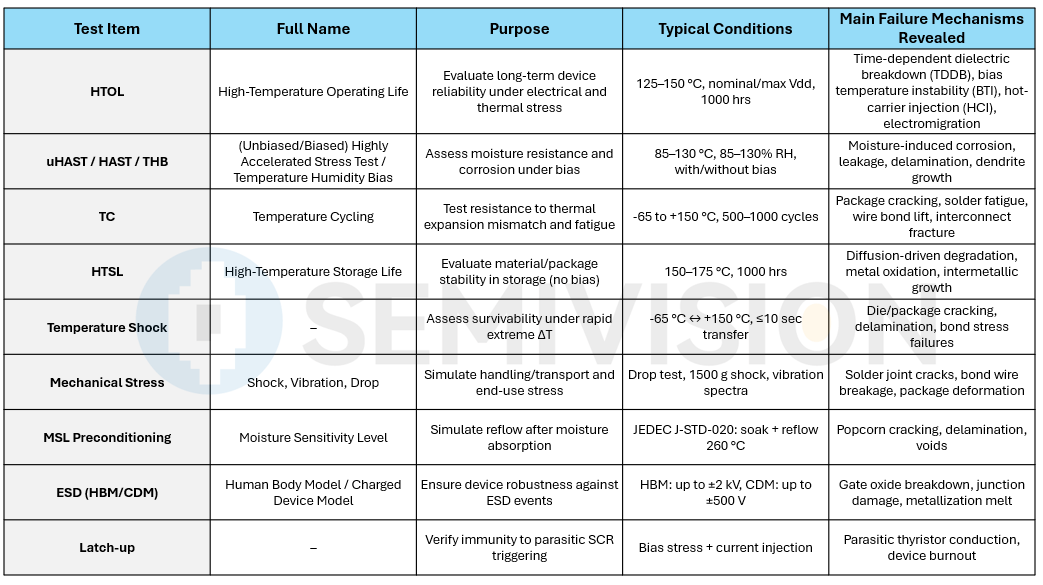
Reliability testing (R-Test) evaluates a product’s ability to withstand environmental and operational stresses throughout its lifecycle, establishing failure rates (FIT), early-life failure rates (ELFR), and lifetime distribution models, with accelerated conditions used to project actual lifetime.
Under the JEDEC and AEC-Q100 frameworks, common test items include:
HTOL (High-Temperature Operating Life)
uHAST/HAST/THB (Unbiased/biased Highly Accelerated Stress Test, Temperature Humidity Bias)
TC (Temperature Cycling)
HTSL (High-Temperature Storage Life)
Temperature Shock
Mechanical Stress (shock, vibration, drop)
MSL Preconditioning
ESD (HBM/CDM) and Latch-up
Test plan design defines sample size, qualification level, binning, and stop criteria, while models such as Arrhenius, Eyring, and Coffin-Manson are applied to derive acceleration factors, ensuring representative failure mechanisms are captured. Automotive and industrial-grade products typically require harsher conditions and longer durations. For new packaging technologies (WLCSP, FCBGA, SiP/modules), reliability must also cover material and interface integrity concerns such as popcorn effect, delamination, electromigration/copper migration, and transistor-level degradations (BTI/HCI/TDDB).
R-Test is tightly linked to mass production:
It serves as essential evidence for new product introduction (NPI) and process change notification (PCN) qualification.
Failure analysis (FA) results—such as cross-sectioning, dye-and-pry, FIB/SEM, IR-OBIRCH, thermal imaging, and acoustic microscopy—feed back into design redundancy, material selection, and packaging conditions.
Sample design covers across-wafer radii, across-lot, and across-process corners to avoid bias. Statistically, results are modeled using Weibull or lognormal distributions to estimate η/β and confidence intervals (e.g., 60%/90% CL); in some cases, zero-failure methodology is applied to compute DPPM upper limits.
In high-reliability markets such as automotive, PPAP/CPK and process capability evidence are mandatory, with PCN-triggered requalification often required. Production-oriented ESS/Burn-in acts as reliability screening, complementing qualification-focused R-Test. Together, their goal is to maximize early-failure interception while maintaining field DPPM within target levels—without introducing new failure mechanisms.
Electrical Quality Check (EQC)
Electrical Quality Check (EQC) is a routine re-test mechanism applied to outgoing lots during mass production, used to monitor process and test system stability, identify lot-to-lot shifts, and perform timely corrections. Essentially, it repeats a representative subset of FT/CP with a shortened flow, serving as a “real-time thermometer” for outgoing shipments.
In practice, AQL and sampling plans are defined based on lot size, risk level, and historical performance. Critical KPIs (e.g., threshold voltage, current, I/O impedance, leakage, timing margin, BIST failure rate, interface BER) are selected, with Delta limits and Trend rules applied; once thresholds are crossed, shipment deferment, MRB, and root cause analysis are triggered. To avoid false alarms caused by measurement system drift, EQC must include Measurement System Analysis (MSA), with regular checks using golden samples, retests/cross-tester comparisons, and Gage R&R to isolate variation sources; corrective actions include calibration, wire/socket replacement, and program revision.
When lot shifts are detected, engineering traces back to WAT and inline metrology for cross-checks to verify whether recipe, material lot, or equipment changes are responsible; if due to test socket aging, stability is restored via socket maintenance and cleaning cycles. For complex products, EQC can be integrated with data science models to build real-time SPC dashboards, monitoring multivariate correlations and early warning signs, while correlating with RMA/customer returns to achieve “disturbance shutdown before shipment.”
Automotive customers often include EQC as part of PPAP and OQC, requiring traceable release reports, limit change records, and lot genealogy; cloud/datacenter customers compare results against SLT/OBA on their side to ensure test platform and software version consistency. On mature lines, skip-lot or dynamic sampling strategies are adopted based on risk, balancing quality control and capacity efficiency.
System-Level Test (SLT)
System-Level Test (SLT) validates the real behavior of chips in near-practical board/system environments, capturing issues that ATE cannot cover, such as interoperability, power-up initialization, firmware handshakes, and long-term stability.
An SLT platform consists of dedicated motherboards, production sockets, and thermal solutions, combined with power sequencing control, reference clocks, programmable I/O emulators, fault injection, and automated firmware/driver frameworks. Test content spans from power-on boot, PLL/clock locking, memory training, to high-speed interface (PCIe/CXL, Ethernet/SerDes, HBM/DDR) link training, BER monitoring, and throughput tests, followed by application-level workloads (encryption/decryption, video transcoding, database stress, AI inference/training fragments) under long-duration operation and thermal cycles.
Compared to ATE, SLT provides higher realism and cross-component integration; however, the tradeoffs are longer test times, high capacity occupation, and costly fixture/software maintenance. Thus, SLT is strategically balanced with FT/Burn-in: high-risk functions are expanded in FT, while system integration risks are shifted to SLT for extended validation, using sampling or conditional triggers to optimize costs.
For high-power AI/networking chips, SLT must incorporate real thermal boundaries—heatsinks, clamping force, airflow ducts, BMC/telemetry, and power modules—to evaluate stability under thermal saturation and transient loads. To enhance insights, engineers build logging/telemetry systems that upload voltage/current/temperature/clock/BER metrics and firmware logs into data lakes, enabling feature extraction and machine learning–based failure mode classification. This accelerates root-cause isolation between firmware, silicon, packaging, or power/thermal boundaries, with knowledge fed back into ATE vectors and DFT strategies to shorten future test times.
On the capacity side, multi-socket parallelization or farm-style racks are deployed, paired with airflow/cold-plate thermal solutions and schedulers optimizing job orders and soak configurations. For ultra–high-value devices, risk-based sampling and conditional triggers (e.g., only applying SLT to CP/FT boundary samples or process-corner lots) achieve the best balance between cost and escape rate.
Ultimately, SLT, FT, CP, and WAT form a closed loop: through cross-stage data correlation and causal analysis, real system issues are brought upstream for resolution in design and manufacturing.
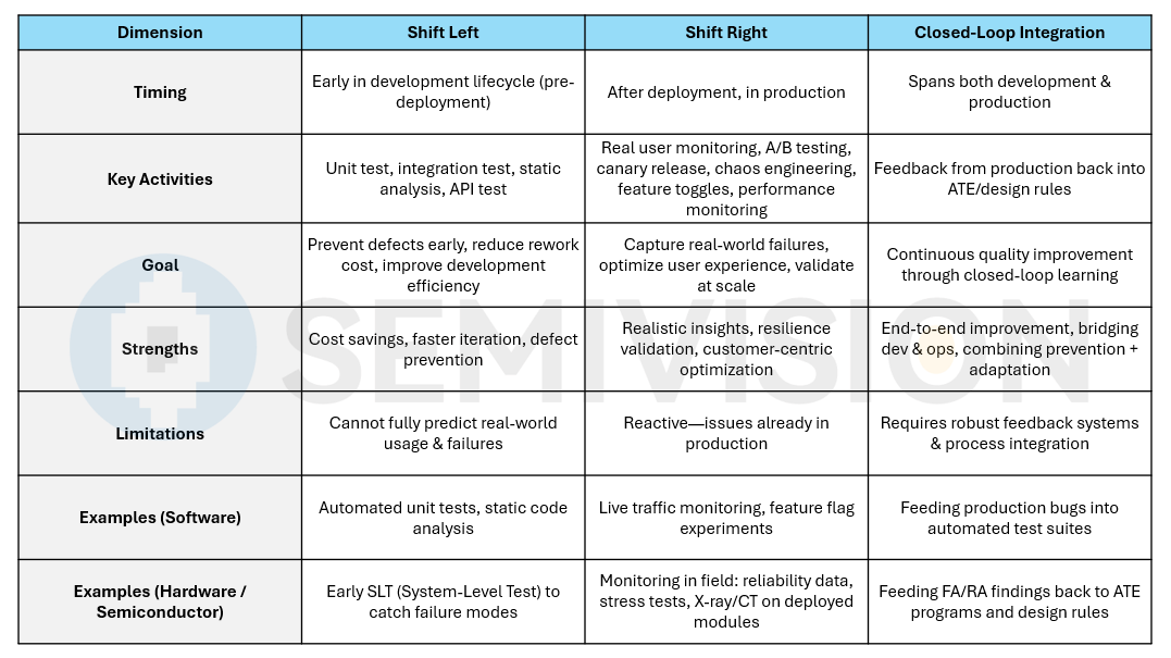
In modern test strategies, a common approach is “Shift Right + Shift Left”: first capture system-level failures through SLT, then feed the failure modes back into ATE and design rules, creating a closed-loop optimization cycle.
“Shift Left” Testing
Definition:Shifting testing activities earlier in the development lifecycle—for example, unit testing, integration testing, static analysis, and API testing—so that verification begins before software is deployed. This reduces the chance of defects propagating into later stages, lowering the cost of fixing issues and improving both quality and efficiency.
Value:Catch errors earlier, reduce the high cost of fixing late-stage defects, and support rapid iteration and continuous delivery.
“Shift Right” Testing
Definition:Conducting testing or monitoring in theproduction environmentafter deployment, including real user behavior analysis, A/B testing, canary releases, chaos engineering, feature toggles, and performance monitoring.
Value:Capture real-world scenarios and failure modes that are difficult to predict in pre-production, gather actual user feedback, and continuously optimize product stability and user experience.
Creating a Closed Loop: Integrating Shift Left + Shift Right
The core idea of this strategy is:
Shift Left:Capture potential defects and failure modes early in development through simulation environments or structured testing processes.
Shift Right:Validate system behavior in production, observing real failures or performance bottlenecks.
Feedback Loop:Feed failure modes detected in production back into ATE (Automated Test Equipment) or design rules, improving both design and testing processes to form a cycle of continuous optimization.
This closed-loop mechanism is a common quality improvement strategy in modernDevOpsas well ashardware validation(e.g., semiconductor testing).
“Shift Left + Shift Right” is a testing strategy: capture failure modes early at the system level (e.g., SLT), then feed these back into ATE and design rules to optimize the overall design and test process—creating a continuous closed-loop improvement cycle.
Core Test Technologies and Equipment: Bringing ATE Capabilities “Onto” the DUT

Pin Electronics (PE) and PMU
PE is the heart of the ATE, serving as the critical interface that “moves measurement capability onto the DUT pins.” A digital PE channel typically consists of a driver, comparator, level generator, and timing gate, enabling precise control of VIH/VIL and VOH/VOL, edge slew rate, and hold time, while per-pin strobe windows are used for logic-level determination. To support fine pitch and high pin-count multi-site testing, PE must also manage simultaneous switching noise (SSN) and return paths to avoid misjudgments under high parallelism.
For mixed-signal or power-related measurements, thePMU (Precision Measurement Unit)provides FVMI/FIMV mode switching and auto-ranging, employing triaxial and Kelvin four-wire force/sense separation to eliminate line resistance and thermal drift. Resolution and linearity at the pA–mA and μV–V scale are fundamental in differentiating platform tiers. In practice, programmable current/voltage clamps and transient protection are added at the PMU front-end to prevent ESD/EOS events from propagating to instrument-grade ADC/DACs. If abnormal surges are detected (e.g., hot-insert or socket contact bounce), the path is shut down within microseconds, and a fault flag is recorded for traceability.
To improve efficiency, ATE systems implement resource virtualization: high-precision PMUs, RF sources, and VI supplies—being scarce resources—are shared across multiple sites through matrix/relay switching. Vector compression and parallel scan techniques are used to shorten pattern lengths. TypicalDC tests(open/short, leakage, ESD diode I–V, gate leakage) use binary search or slope fitting to estimate thresholds, while high-speed I/O leverage built-in loopback/PRBS and BER threshold measurements. Memory repair/trim (eFuse,OTP) and ID/key programming are also executed through PE/PMU, followed by immediate retesting for verification.
To suppress parasitic leakage in nanoamp-level measurements, the load board and socket require guarding and driven guards, with critical traces built from Teflon/low-leakage materials and designed to avoid contamination and flux residues. For high-current paths (e.g., AI/HPC chips drawing tens of amperes at power-up), PE and VI supplies must provide low-impedance delivery with fast current compliance slew, preventing power-up resonance, IR droop, and repeated resets.
Finally, the accuracy of all PE/PMU operations depends on strict metrology traceability: calibration with NIST-traceable standards, golden fixtures, and golden DUTs is performed regularly to correct gain, offset, and temperature coefficients. Calibration factors are then bound to lot, tester, and program version within the MES, ensuring cross-site consistency and full traceability.
Timing and Calibration
High-speed devices under test (DUTs) — such as SerDes, DDR, PCIe, CXL, and HBM — are extremely sensitive towhentest vectors are applied andwhenresponses are sampled. Therefore, per-pin timing sets, deskew, and jitter management are the dividing line between success and failure in measurements.
The ATE timing tree forms a long transmission path, spanning from instrument clocks through the test head, test socket, and finally to the load board. Each segment exhibits unique group delays, distribution delays, and temperature coefficients. Engineers use loopback, delay lines, or TDR/eye-diagram golden samples to estimate the true at-pin timing. A path model is then built, and per-pin deskew is applied to align strobes and edges down to the picosecond level.
Jitter must be decomposed into random (RJ) and deterministic components (DJ, ISI, periodic, crosstalk). The intrinsic jitter of the ATE must be suppressed to within one-tenth of the DUT specification, otherwise the results will be tester-limited. For CDR/PLL-based interfaces, lock behavior and wander must be considered, with training sequences, SSC (spread-spectrum clocking), and jitter tolerance faithfully reproduced in patterns.
Calibration extends beyond timing. PMU gain/offset, VI supply voltage/current feedback, and ATU thermal delta must all be regularly maintained under a closed-loop regime ofcalibration → verification → correlation (CP/FT/SLT) → monitoring. Test programs undergo version freeze before release and are validated with golden samples across multiple temperatures and testers. In production, dynamic limits (DLimits) and guard-banding are applied to absorb short-term drift. When critical KPIs show cross-tester shifts, SPC and pairwise correlation are used to check the triad of instrument/fixture/program; rollback or re-characterization may be triggered if necessary.
For ultra-high-speed links, timing calibration extends into BER measurement windows and FEC-related parameters, ensuring error statistics are not biased by window offsets or PRBS initialization artifacts. In memory and logic at-speed testing, Shmoo (V-F-T) scans and on-die monitors (temperature, IR drop, clock) quantify the correlation among timing, power, and thermal domains, pushing measurement uncertainty below decision thresholds.
Shmoo (V-F-T)
Shmoo testing (Voltage–Frequency–Temperature) is a method to sweep parameters such as voltage, clock frequency, and temperature to analyze whether a chip can operate correctly under different conditions. By plotting Shmoo diagrams, engineers can visually identify operating margins and failure mechanisms. This tool greatly enhances both early design validation and later high-volume failure analysis, improving test efficiency and debug capability.
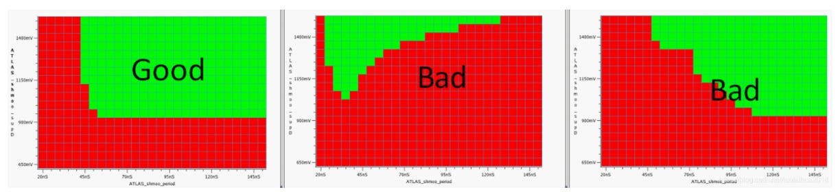
As shown above, when the CPU runs a diagnostic test program, the ROS offset voltage and clock frequency are variable, represented by the horizontal and vertical axes respectively. At a given voltage and frequency, if the diagnostic test passes, it is marked in green (pass); if it fails, it is marked in red (fail). By continuously running the diagnostic program across a range of voltages and frequencies, and then plotting the results, a Shmoo diagram can be generated.
To pass the test, the Shmoo diagram must be sufficiently large to include a rectangle, which represents the minimum tolerance range of offset voltage and timing delay with zero error margin. The optimal ROS offset voltage and timing delay are indicated by a single point at the center of this rectangle.
Load Board and Signal Integrity
The first gate to reliably “transfer ATE capability onto the DUT” lies in the signal chain of load board, socket, pogo pins, and connectors. High-frequency design starts with material choice: low-Dk/Df substrates, controlled-impedance routing, GSSG differential layouts, via back-drilling, microvias, and via-fences for return paths.
For power integrity (PI), the stack-up and decoupling network must be designed around target impedance (Ztarget), handling large current steps and suppressing LC resonance to prevent Vdroop-induced timing misjudgments during at-speed testing.
Calibration relies on TDR to extract at-socket/at-pin impedance discontinuities and validate connector/via models. VNA provides S-parameters (IL/RL/crosstalk), with TRL or 2x-thru de-embedding to strip out fixture/socket parasitics and preserve the “true DUT” response.
In multi-site setups, station-to-station coupling (crosstalk, ground bounce) can amplify, requiring careful ground referencing and isolation zoning. For RF/mmWave paths, short coaxial or flex-coax connections should be used directly to the socket, avoiding unnecessary FR-4 routing.
Socket resistance and parasitics drift with insertion count, temperature, and contamination. Production requires maintenance cycles and in-situ health checks (e.g., 4-wire resistance distribution, IL/RL drift monitoring, calibration pulse reflection checks). Critical lanes should be benchmarked with golden channels to rapidly identify fixture aging or local contamination.
For high-speed SerDes, the ATE must support equalization parameters (CTLE/FFE/DFE) download and readback, with fixed training sequences and initialization to avoid cross-site differences. For memory interfaces, load board topology (T-branch, stub length), termination location, and ODT settings must match datasheet/NPI design. Otherwise, eye margins may collapse despite DUT compliance. In short, robust SI/PI design and consistent de-embedding/models are prerequisites to deliver undistorted ATE accuracy to DUT pins.
Thermal Management
Temperature is the “hidden independent variable” in all electrical measurements. Tri-temp testing (low/room/high) is costly because the challenge lies in stabilizing DUT junction temperature (Tj) at target points, with small ΔT and high repeatability during measurement.
The handler/ATU (active thermal unit) and socket dominate the thermal resistance chain: θCA (cold plate to ambient), θCS (cold plate to package lid), θJC (package lid to die). Poor contact or degraded TIM (thermal interface material) amplifies Tj errors. TIM options include grease, phase-change materials, and graphite pads, combined with controlled clamp force and extrusion specs to ensure consistency across insertions. Cooling can be mechanical (TEC, vortex, compressor) or cryogenic (LN2, ethanol bath). Mechanical is cost-effective, cryogenic enables ultra-low setpoints but requires condensation/safety management.
Production balancing between thermal soak and throughput involves thermal modeling of power-to-ΔT, soak times, preheat/precool profiles, and workload distribution to avoid Tj drift around high-power vectors. On-die sensors (thermal diodes, digital monitors) or IR thermography validate uniformity and stabilization time.
For AI/HPC large-die and HBM/SiP modules, heat non-uniformity is pronounced. Socket geometry, airflow, and clamping optimization are critical; cold plates or liquid-cooled fixtures may be needed for high heat flux. To avoid thermal–electrical interactions, power-aware vector scheduling and soft-start suppress inrush and IR droop at high Tj.
Environmental control adds complexity: low-temp tests require dehumidification, nitrogen purging, and dew-point monitoring; high-temp requires socket/carrier aging and creepage checks. ATU feedback must be calibrated, with stored conversion curves linking ATU setpoint to Tj, preventing hidden inter-site offsets.
The ultimate goal: ensure the same DUT, on any tester, at any time, is measured at the same Tj and thermal boundary conditions — so binning and release decisions reflect product performance, not test environment variability.
Test Specifications and Datasheet Alignment: One Unified Ruler from Design to Production
The core of spec deployment lies in ensuring that parameters are consistently defined across worlds: design simulation, first-silicon, ATE measurement, and system implementation.
The flow begins with Design Specs, establishing nominal device/interface behavior in SPICE and SI/PI simulations, with Monte Carlo and layout effect sampling to capture distributions. This is followed by sensitivity analysis across voltage, temperature, frequency, and load. For interface-class specs (SerDes eye, jitter tolerance, DDR training convergence), “testability” is validated early with channel and noise models to avoid blind spots that can’t be replicated on ATE.
When silicon arrives, aSilicon-to-Simulation (S2S)loop is established: structural tests, Shmoo (V-F-T), and on-die monitors collect actual distributions, fed back into models for bias/gain correction. Statistical assumptions like OCV/AOCV/POCV are adjusted to align timing/power/noise corners with real silicon.
Datasheet min/typ/max specs are then mapped toTT/SS/FF/SF/FS cornersand extreme PVT points, with explicit measurement conditions (VDD, temp, load, terminations, methodology). The Test Spec encodes all ATE details: vectors, timing windows, de-embedding files, instrument resolution/uncertainty, socket/load board parasitics, power preconditions, ATU settings.
Device Corner Plot — TT/SS/FF/SF/FS Corners
In semiconductor manufacturing, the concept ofcornersis used to describe transistor and circuit performance variations arising from process deviations. Factors such as doping concentration, diffusion depth, etching precision, and annealing efficiency introduce variability across wafers, dies, and even batches. To accurately capture these effects, the industry employs thePVT model (Process, Voltage, Temperature), where theProcessdimension is further subdivided into corners such asTT, SS, FF, SF, FS. The two letters correspond to NMOS and PMOS speed conditions, withT = Typical, S = Slow, F = Fast.
In digital circuit analysis, TT/SS/FF corners are typically sufficient, whereas analog circuit analysis often requires SF and FS as well. Together, these five corners broadly cover the ±3σ (~99.73%) process variation space.
Corner analysis serves as an alternative to Monte Carlo simulations, by combining extreme parameter cases to evaluate worst-case and best-case performance scenarios. Variations in threshold voltage (Vt), mobility (μ), and oxide capacitance (Cox) directly affect switching speed and leakage behavior. For example:
SS (Slow-Slow):Higher Vt, reduced IDS, slower switching, lower leakage.
FF (Fast-Fast):Lower Vt, higher IDS, faster switching, but significantly increased leakage.
Voltage and temperature corners extend the analysis: supply voltage shifts impact both speed and power, while temperature extremes (low/room/high) reveal thermal sensitivity. Through PVT and corner modeling, designers ensure circuits function reliably under worst-case conditions, safeguarding both yield and product reliability in high-volume manufacturing.
Guardbands — Definition and Rationale
Aguardbandis a tighter limit than the datasheet specification, applied during calibration and verification to account formeasurement uncertainty. Rather than relying on engineering intuition, guardbands are derived fromrisk-based statistical modeling. Their purpose is to reduce the probability offalse rejects (Type I errors)andfalse accepts (Type II errors)in semiconductor testing.
Why not intuition?
Guardbands are not arbitrarily chosen; they are calculated based on risk analysis and measurement system performance. Specifically:
Identify error sources at every stage (instrument specs, de-embedding residuals, fixturing/contact resistance, operator variation).
Quantify combined uncertainty (Uc), often by root-sum-of-squares of individual contributions.
Apply a coverage factork(e.g., k = 2 for 95% confidence) to obtain expanded uncertainty (U = k × Uc).
Define guardband width accordingly (e.g., Effective Tolerance = Spec Limit − U).
This approach ensures the test pass/fail boundary is set scientifically, balancing risks against DPPM (defective parts per million) quality goals.
Application in Semiconductor Testing
In semiconductor ATE environments, multiple error sources accumulate: tester precision limits, probe card contact resistance, load board parasitics, IR drops, thermal gradients, timing jitter, and long-term drift. If only the nominal spec limits were used, two risks emerge:
False Fail (overkill):good devices incorrectly rejected, reducing yield.
False Pass (escape):bad devices incorrectly accepted, undermining field reliability.
Guardbanding integratesMeasurement System Analysis (MSA), tester-to-tester correlation, and error budgeting into risk models, ensuring that capability indices (Cpk/Ppk) reflectthe product’s true distribution rather than tester artifacts.
Thus, in semiconductor test engineering, the principle“guardbands are not based on intuition, but on quantified uncertainty and risk models”is fundamental to achieving both yield efficiency and product reliability.
- Defining the Role of Guardband
In semiconductor testing processes (CP / FT / SLT), aGuardbandis primarily used to adjust the decision boundary forPass/Fail judgments.
Without Guardband:The device is evaluated directly against the datasheet specification (e.g., ±5% voltage range).
With Guardband:The specification window is tightened according to the measurement system’s uncertainty (e.g., ±5% → ±4.7%), ensuring that even with error margins, defective parts will not be falsely accepted.
In essence, a guardband creates a“protection zone”between the measured test results and the true specification limits.
- How to Integrate Risk Models with Measurement Uncertainty
Quantifying Sources of Uncertainty
ATE system accuracy:channel measurement errors, digital conversion precision, timing resolution.
Probe and load board effects:contact resistance, parasitic capacitance, parasitic inductance.
Environment and temperature:ΔT drift (DUT drift) and IR drop under different thermal conditions.
Operation and statistics:random variations across repeated measurements.
Combining Uncertainty
Use Root Sum Square (RSS) or statistical combination methods to obtain theCombined Measurement Uncertainty (Uc).
Multiply by a confidence factork(e.g., 95% corresponds to k=2) to obtain theExpanded Uncertainty (U).
Designing Guardbands
Formula example:Guardband = Spec Limit – U
(Apply this range to the test program decision logic to keep risk under control.)
- Practical Application Scenarios
CP (Wafer Probe):Because probe contact uncertainty is large, guardbands are often set conservatively to reduce the risk of shipping bad dies.
FT (Final Test):ATE is more stable, so guardbands can be closer to spec, avoiding excessive false fails.
SLT (System-Level Test):Since thermal/power drift is significant, guardbands must integrate ΔT drift models, incorporating thermal effects and aging risks.
High-Reliability Products (Automotive/Medical):Guardbands are usually stricter, as the cost of passing a defective part is extremely high.
- Industry Best Practices
Dynamic Guardbanding:Guardbands adjust automatically based on lot or tester calibration status, instead of being a fixed value.
Closed-Loop Optimization:Failure modes observed at SLT are fed back to ATE to recalculate the uncertainty model and update guardbands.
Risk-Oriented Decisions:Combine Monte Carlo simulations with corner analysis to predict failure rates across PVT conditions, and refine test strategies via guardbanding.
In the field of testing and measurement,DUT drift (Device Under Test drift)generally refers to the performance deviation of a device under test caused by factors such as temperature rise and changes in internal resistance during power-on or operation.
In short: In semiconductor testing, a guardband translatestest system errorsinto arisk modelthat is integrated into spec-based decisions. This ensures that under high-volume production conditions, products are neither over-rejected nor falsely accepted—making guardbanding a critical tool for both test quality and yield control.
- Warm-up Drift
Definition:When an electronic device is first powered on (or when testing begins), its internal circuitry experiences temperature changes due to power application, leading to time-dependent drift in performance parameters. This phenomenon is known aswarm-up drift.
Mechanism:Current flowing through components generates Joule heating, causing the internal temperature to rise. As the temperature stabilizes, the measured values also stabilize, typically within a few minutes.
Example:In force gauges or strain-gauge-based sensors, warm-up drift may cause the readings to shift initially before stabilizing.
- IR/ΔT Drift (Resistance–Temperature Rise Drift)
IR Drift:Here,IRrefers toInternal Resistance, which varies as temperature rises. These changes can affect the measurement signals or device performance. In short, temperature rise induces internal resistance drift, altering output characteristics.
ΔT (Temperature Difference) Effect:Temperature differences within the device, or between the device and its environment, impact measurement accuracy. For example, in Wheatstone bridge-based sensors, if the four resistors heat unevenly, a temperature gradient occurs, leading to drift in the output.
The Meaning of SPC and Process Capability Indices
SPC (Statistical Process Control):
The purpose of SPC is to use statistical methods to monitor the production process, ensuring that it remains within capability limits and stays stable over time. Beyond control charts for trend monitoring, process capability indices—Cp, Cpk, and Ca—are used to quantify how well a process performs relative to specification limits.
Applications in Semiconductor Testing
Wafer Test (CP):Cp and Cpk are used to evaluate the distribution stability of electrical parameters such as threshold voltage, leakage current, and delay time, which directly impacts die yield.
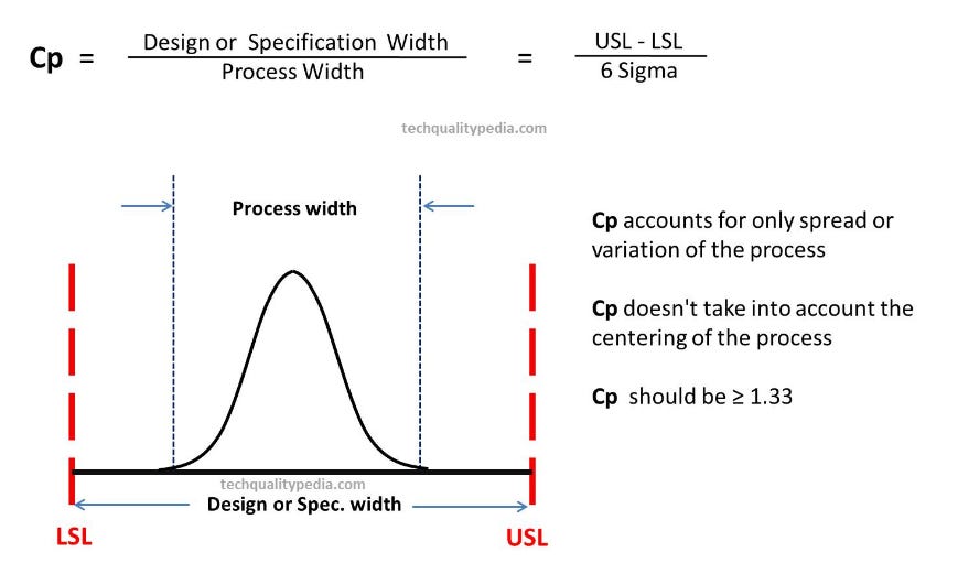
Final Test (FT):Cpk is applied to monitor tester precision and offset, ensuring measurement errors do not compromise Pass/Fail decisions.

System-Level Test (SLT):Ca becomes particularly important, since temperature and voltage drifts can shift the distribution mean, and it must be verified that the process remains within acceptable ranges.
Key Takeaways
Cp:Measures inherent process capability (spread relative to spec).
Cpk:Measures process capabilityplus offsetfrom the target.
Ca:Measures thedegree of mean shift.
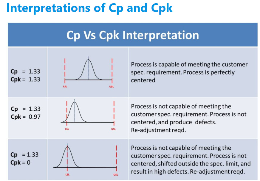
Source: techqualitypedia
Release thresholds are back-calculated from yield and quality goals: consumer devices often require Cpk ≥ 1.33, automotive Cpk ≥ 1.67. Actual lots are tracked via Ppk drift. Non-Gaussian or long-tail distributions are handled with quantiles or EVT instead of normal assumptions.
PAT (Part Average Testing)and Outlier Screening must be pre-designed: dynamic windows on mean/std within wafer/lot/site, multivariate Z-score or Mahalanobis distance for correlated parameters (IDDQ, leakage family, frequency margin, BER, training iterations), with spatial PAT (GDBN) to catch clustered defects. PAT rules are validated in NPI with S2S samples to balance escape vs overkill, tightly coupled with FA.
Basic Concept of PAT
Traditional Testing Approach:Pass/Fail judgments are made solely based on datasheet specification limits (USL/LSL).
Problem:Some defective or marginal dies may still fall within spec but show abnormal deviation compared withother devices in the same lot→ such parts may fail later in the field.
PAT Method:Statistical analysis is performed on test data from the same lot or wafer. For each test item, the mean and standard deviation are calculated, and individual device data is compared against this distribution. If a device’s result deviates excessively from the mean, it is flagged—even if it is still within the datasheet limits.
In short:PAT doesn’t rely only on datasheet specifications; it also detectsoutliers relative to the population average.
Applications and Value
Automotive Electronics (AEC-Q100 requirement):PAT is mandatory to identifypotential early-life failures, ensuring long-term reliability.
High-Reliability Products:In sectors likemedical, military, and aerospace chips, PAT helps prevent “latent defective dies” from escaping into the field.
Semiconductor Mass Production Testing:PAT runs in parallel with traditional spec-based testing, providing enhanced yield analysis and stronger defect prevention.

Source: Anne Meixner/Semiconductor Engineering
PAT (Part Average Testing)is a statistical method used in semiconductor testing to screen out abnormal chips. Traditional pass/fail criteria rely solely on datasheet specification limits, which may allow potentially defective chips to pass if they fall within the limits but significantly deviate from the distribution of other chips in the same lot. The core principle of PAT is to perform statistical analysis at the lot or wafer level, calculating the mean and standard deviation of test data, and comparing each device’s result against this distribution. If a data point falls outside the μ ± Nσ range, it is flagged as a PAT fail. This approach is especially common in high-reliability applications such as automotive, aerospace, and medical devices, and is mandated under theAEC-Q100standard to complement traditional specification-based testing and prevent latent defects from reaching the market.
In practice, duringmass productionandNPI (New Product Introduction)phases, PAT andOutlier Screeningare not limited to fixed thresholds but must be designed with predefined rules and dynamic adjustments. For example, at the wafer, lot, or site level, sliding windows are used to continuously update means and standard deviations. In multivariate cases,Z-scoreorMahalanobis distanceis applied to evaluate anomalies across multiple correlated parameters (e.g., IDDQ, leakage clusters, frequency margins, BER, training iteration counts). Furthermore,Spatial PATis introduced, leveraging theGDBN (Good Die, Bad Neighborhood)method to detect clustering defects on the wafer that might otherwise be masked by global statistics.

Source: yieldwerx
These PAT rules must be validated during NPI through site-to-site sampling to balance the risks ofescapes(defective parts shipped) andoverkill(false fails of good parts). In addition, PAT must work in close collaboration withFailure Analysis (FA)to form a closed-loop optimization between testing and root-cause analysis.
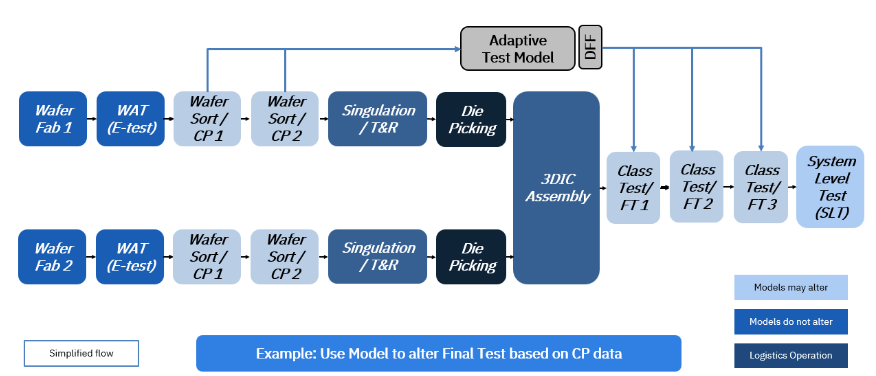
Source: PDF Solutions
In modern semiconductor testing, the traditional reliance on fixed specification limits is gradually evolving into an intelligent strategy centered onDynamic Limits (DL)andAdaptive Test (AT).
DL dynamically adjusts limits based on wafer-, lot-, or site-level statistical data, absorbing process or measurement drifts and reducing the risks of false fails and escapes. AT leverages the correlation and modeling between wafer test (CP) and final test (FT) to determine which tests can be shortened or skipped, thereby reducing test time and cost. If anomalies or borderline samples appear, the system automatically falls back to full testing, ensuring that risks are not overlooked.
All adaptive logic must be safeguarded with safety nets, such as minimum coverage thresholds, cross-site sampling, periodic re-characterization, and strict version control through the MES system combined with PCN workflows, ensuring every adjustment remains traceable.
Furthermore, the industry is pushing towarddigital integration of Datasheets and Test Specifications, establishing aSingle Source of Truth. Each datasheet parameter must be mapped to a unique Test ID, measurement method, and error budget. Once a model or recipe is updated, associated limits, de-embedding algorithms, and Golden Sample references are simultaneously refreshed. Before Test Program release, correlation reports across sites, temperatures, and lots must be completed to prevent rule divergence.
This way, from design to mass production, engineering, product, test, and quality teams all operate under acommon measurement framework, where specifications are no longer just text on paper but ameasurable, auditable, and continuously improvable digital system.
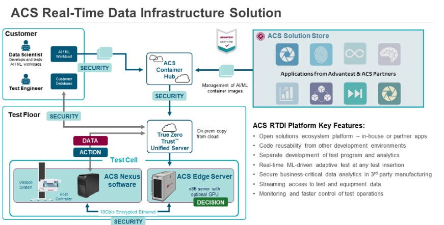
Source: Advantest
Dynamic Limits (DL)andAdaptive Test (AT)reduce cost/time under risk control: DL adjusts limits by lot/wafer/site statistics to absorb drift; AT leverages CP↔FT correlations and models to decide skip/shortened tests, with fallback to full coverage for outliers. All adaptive logic must have safety nets: minimum coverage, boundary samples, cross-site sampling, periodic re-characterization, with strict MES version control and PCN workflows for traceability.
Finally, the Datasheet and Test Spec are bound into a single source of truth: each datasheet spec maps to a unique Test ID, method, and error budget. Any model/recipe update propagates to limits, de-embedding, and golden sample baselines. Test program updates require correlation reports across sites/temps/lots before release.
This ensures that from design to mass production, engineering, product, test, and quality teams operate with the same ruler, and specifications become measurable, auditable, and continuously improvable systems — not just words on a document.
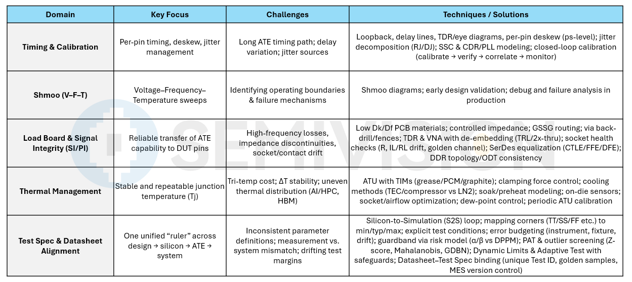
Common Test Items: Practical Highlights in DC / Functional / AC
DC (Connectivity and Basic Electrical Tests)
DC testing is the first gate in mass production, aiming to quickly and cost-effectively screen out obvious defects and establish safe conditions for subsequent measurements. Typically, Open/Short (O/S) and Power Short are performed first: using the PMU to force a small current (Force I) and measure voltage (Measure V), or vice versa, to check if each I/O pin’s diode conduction to VDD/VSS falls within spec, thereby detecting opens, shorts, and damaged ESD structures. To avoid EOS induced by the test itself, voltage/current clamps and slew rate limits are applied. The load board/socket is built with Kelvin four-wire and driven-guard techniques to suppress leakage.
Before power-up, a “pre-power” scan checks for low-impedance shorts on the power network, and I–V sweeps at multiple voltage steps distinguish real shorts from capacitor charge/discharge. IIL/IIH and VOH/VOL tests verify input/output logic levels against datasheet specs: inputs use small-current sweeps to observe threshold/hysteresis; outputs measure VOH/VOL and drive strength under controlled loads, recording static margins. Power current tests include IDDS (standby), IDDD (operating), and IDDQ (static leakage). IDDQ is sensitive to noise at advanced nodes, requiring temperature, IR droop, and SSN control; it is often measured in low-frequency or frozen-clock windows, sometimes partitioned or compared as ΔIDDQ on large die to improve resolution. For multi-power-domain products, each domain is measured independently with checks for isolation and gating states.
PAT/Outlier rules are applied, e.g., Z-score or Mahalanobis distance to filter excessive leakage, abnormal diode voltages, or atypical VOH/VOL combinations. Wafer/strip map spatial info supports GDBN (Good-Die-in-Bad-Neighborhood) screening. DC tests are sequenced early to maximize time/cost savings and cross-checked between CP and FT.
Cross-site drifts trigger inspection of contact resistance, cleaning cycles, socket clamping, and de-embedding files. Ultimately, success in DC testing depends on protective limits, leakage control, and statistical filtering, ensuring later functional and AC tests don’t waste resources on inherently bad devices.
Functional (Vector Verification and DFT Coverage)
Functional testing aims to approximate an infinite state space within finite test time, requiring close reliance on DFT. Mass-production SoCs typically use scan ATPG to cover stuck-at, transition, and path-delay fault models. Scan compression reduces vector volume via on-chip phase shifters/compactors, while X-masking prevents unknowns from corrupting MISR signatures.
LBIST with LFSR/MISR enhances parallelism and independence from external vectors, suitable for large digital arrays and automotive re-test. MBIST applies March, Checkerboard, GALPAT, etc., with redundancy repair (eFuse/OTP). Post-repair, re-test and UID/key programming must be verified. Vector ordering follows power-aware scheduling: low-risk vectors first for health checks, gradually ramping to at-speed critical paths, with recovery vectors interleaved to stabilize power and temperature.
For protocol-based ICs (PCIe, CXL, Ethernet, Display, Imaging), the ATE must provide deterministic boot and handshake tools, fixing training parameters and clock sources to avoid site-to-site variation. Cross-domain/security-domain testing requires authorization and isolation checks to ensure no escapes due to inconsistent definitions among design, process, and test.
Coverage must link todefect density (D0),escape rate, andDPPMgoals, with weighting for dominant fault classes. Scan diagnosis and layout-aware analysis accelerate correlation with process/layout regions, aiding FA and yield ramp. Functional tests complement SLT: ATE ensures reproducible logic/protocol correctness, while SLT validates long-term stability, interoperability, and firmware interaction. Linking their fail modes in a common data lake allows boundary conditions to feed back as new vectors and limits.
Only when the DFT strategy, vector design, power/thermal management, and diagnostic loop are unified can functional testing avoid the pitfalls of “time explosion” or “illusory coverage.”
AC (Timing and High-Speed Interface Characterization)
AC testing focuses on “how fast” and “how reliable at boundaries.” This spans pin-level rise/fall times, propagation delays, setup/hold margins, extending to eye diagrams, jitter tolerance (JTOL), and voltage/time sweeps for SerDes and DDR interfaces.
Pin-level AC relies on per-pin timing and deskew, using calibrated references to align strobes, stepping delays to build input/output timing curves, and sweeping PVT with Shmoo (V–F–T) to capture sensitivities. These results feed directly into datasheet values (tSU/tH, tPLH/tPHL, fMAX). DDR interfaces combine read/write training, Vref sweeps, and ODT/termination settings to extract eye height/width and timing mask margins. For SerDes, ATE/instrument support includes programmable jitter injection (RJ/DJ/SSC), channel loss/crosstalk models (S-parameters/fixtures), and Tx equalization (pre-/de-emphasis), while Rx convergence and BER build bathtub curves and tolerance surfaces.
To ensure at-tester-pin equivalence to spec-defined test points (TPs), strict de-embedding (TRL, 2x-thru) removes fixture/socket parasitics. Without this, eye/JTL results risk being fixture-limited. Mass-production converts “long characterization tests” into “short release tests” via correlation models built during NPI (e.g., limited PRBS31 sampling predicting full BER curves). Production uses quick scans or fixed-stress fast screens, with deep sweeps triggered only for boundary samples. Shmoo results feed binning and dynamic limits absorb drift.
AC testing must be power- and thermal-aware: high-speed vectors create transient power/thermal surges that shrink timing/eye margins via Tj drift. Programs insert cooling/stabilization windows, use on-die thermal feedback to adjust strobes, and sequence vectors to suppress IR droop.
Compliance products require matching industry masks/JTL specs, saving training logs and EQ settings for reproducibility. Cross-site drifts prompt checks on S-parameters, de-embedding files, ATU settings, socket aging, and phase noise.
In summary, AC’s essence is “calibrate to pin, equate to spec, shorten for throughput” — transforming characterization truths into production-worthy release flows without losing fidelity.
DFT and Memory Testing: Designing Testability In
ATPG and Fault Models
To achieve acceptable DPPM in high-volume manufacturing under limited test cycles, the key is to translate the "most probable and most risky" defect types into testable vectors already at the design stage. The basic ATPG models are stuck-at (node stuck-at-0/1) and bridging (metal bridging): the former is sensitive to opens and via failures, while the latter detects weak shorts and resistive coupling common in advanced BEOL with tighter line/space dimensions. More advanced fault models include transition/path-delay and small-delay-defect (SDD), covering edge slowdowns and marginal increases in critical path timing to catch failures that may only appear under low-voltage, high-temperature, or aging conditions.
For advanced nodes (FinFET/GAA), where internal parasitics and variations are significant, Cell-Aware ATPG (deriving fault observability from transistor-level defect libraries) has become standard practice, significantly improving early failure and “hard-to-catch” defect coverage. ATPG is not merely about generating more patterns—it must consider test power (switching density), IR droop, X-sources (unknown values), and multi-power-domain constraints. Techniques include power-aware fill to limit switching, X-masking/compaction to prevent contamination of signatures, and constraint validation to avoid illegal states.
Coverage goals are not isolated percentages but determined jointly by defect density (D0), chip area, sample size, and target DPPM. Common strategies include N-detect (multiple detections per fault) and layout-aware physical targeting to improve effective coverage, while embedding diagnostic capability (diagnosis-driven yield) so that failing vectors already contain distinguishing power to localize to nets or layout regions, shortening FA cycles. Finally, ATPG is converging with data-driven adaptive test: during mass production, PAT/Outlier screening and on-die monitors guide dynamic selection of the most informative vector subset—maintaining risk boundaries while minimizing test time.
Scan Chains and At-Speed Test
Scan is the backbone of digital DFT, turning uncontrollable/unobservable sequential logic into shift registers. Designers plan chain count/length, domain crossing, lock-up latches, and clock-tree impact; in practice, scan reordering reduces routing congestion and coupling. For production, almost all use compressed scan (e.g., EDT): a small number of ATE channels are expanded by phase shifters into high-dimensional stimuli, while outputs are compacted into MISR signatures with X-masking/filtering for unknowns from analog/mixed-signal blocks. Compression ratio, X tolerance, and aliasing risks must be validated across golden samples and test platforms.
At-speed test is crucial for setup/hold and subtle delay defects, with common launch-on-shift (LOS) and launch-on-capture (LOC) methods. If external ATE clocks are insufficient or jittery, on-chip clock controllers/PLLs (OCC/OCP) synthesize GHz-class clocks gated into target domains, while maintaining safe domain crossings and power sequencing. Challenges include power and thermal issues: massive switching can cause IR droop, ground bounce, and junction temperature drift leading to false fails. Mitigation includes power-aware pattern scheduling, slowed scan-shift, partitioned capture, and cooling intervals. For low-power designs, power-aware ATPG/scan stitching ensures each domain is tested under proper on/iso/retention states. Before release, cross-correlation across testers, sites, and temperatures validates pass/fail boundaries, and scan diagnosis links FA with process learning—ensuring scan goes beyond “coverage numbers” to actionable insight.
Embedded Test Access
As SoCs grow in scale and IP diversity, a "transport network" is needed to bring test and debug access everywhere. IEEE 1500 adds wrappers and TAMs (test access mechanisms) to IP cores, allowing consistent drive/observe of internal scan and BIST. IEEE 1687 (IJTAG) maps on-die monitors, sensors, phase shifters, logic analyzers, droop/temperature/clock detectors, and high-speed margining engines into an addressable instrumentation network, controlled via the TAP for retargeting.
This enables a single test/debug key across bring-up, production, and RMA: used in development for PVT measurement and model calibration; in production for adaptive test (e.g., using droop monitors to decide deeper AC scan); and in the field for remote diagnosis. For 2.5D/3D stacking and HBM, IEEE 1838 introduces die wrappers and TAP chaining to structurally test TSVs/micro-bumps across dies. Embedded access also raises security concerns: to prevent scan/instrumentation leaks of keys and firmware, mechanisms like secure TAP, authorization fuses, scan locking, and black-box signatures are applied, with tiered privileges across manufacturing and field use.
In short, embedded test access transforms "reachability" into a systemic capability—making test, calibration, monitoring, and diagnosis stages of the same data pipeline.
BIST / MBIST / BISR
Memory dominates both the area and failure rate of SoCs; without MBIST and BISR, achieving volume production is almost impossible.
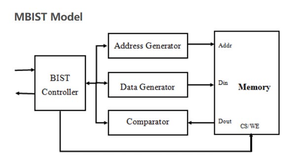
MBIST manipulates memory cells under various stress conditions through algorithmic sequences:
March C-/C+/Y, Checkerboard, Walking 1/0target stuck-at, transition, coupling, and decoder faults.
Retention and Disturb testspause at low voltage, long duration, or high temperature before readout to capture leakage and half-select vulnerabilities.
For eDRAM/eSRAM, extra checks cover write recovery, read disturb, and sense-amplifier timing boundaries.
During NPI, worst-case “corner maps” are built using low Vmin / high-temperature conditions.
BISR passes failing addresses to the BIRA allocator, which assigns spare rows/columns (and sometimes bit/block redundancy) with minimal cost to generate a repair map. This map is stored via eFuse/OTP/laser fuse programming; upon reset, repair logic reroutes accesses, followed by immediate retest verification. Thistest–repair–verify loopis the main driver of yield ramp-up in high-density SRAM/TCAM.

With scaling, ECC and BISR increasingly work hand-in-hand: BISR addresses systematic and large-grain defects, while ECC handles random soft errors and aging. Only co-design ensures the right trade-off among bandwidth, area, and reliability.
To prevent power/IR issues during test, MBIST often uses clock gating, sub-array partitioning, and phase-interleaved algorithms. For automotive/high-reliability devices, MBIST/LBIST is re-executed during power-up or at runtime for self-diagnosis.
In practice, MBIST reporting also links to PAT/outlier handling: e.g., flagging devices with weak retention margins into a risk bin, then applying additional stress tests or down-binning at CP/FT/SLT—balancing quality with yield.
Boundary Scan and High-Speed Interface Testing
IEEE 1149.1 (JTAG) provides the TAP state machine and EXTEST/SAMPLE/PRELOAD instructions, enabling structural verification of board-level interconnects, BGA solder joints, and module connections. IDCODE/BYPASS support multi-device chains and easier debugging.
For AC-coupled differential links (PCIe, SATA, SerDes backplanes), 1149.6 defines structural testing under capacitor-isolated conditions, detecting opens/shorts and termination errors without needing higher-layer protocols.
At very high speeds, structural tests alone are insufficient. SoCs integrate:
PRBS generators/checkers,
BERTs,
Eye diagram scanners,
Margining engines (injecting RJ/DJ/SSC, adjusting Tx pre-emphasis, Rx CTLE/DFE).
These enable link training, margin sweeps, and bathtub curve measurements directly on ATE or SLT. Training logs and equalization coefficients can be read back to diagnose channel, power, or package-related boundary issues.
For DDR/LPDDR/HBM, the controller/PHY runs training steps (Vref, DQS alignment, ODT/termination, write leveling/read gate). Using MPR/fixed patterns for windowing, these results map to datasheet timing/voltage margins.
Production strategy:
Use boundary scan first for quick detection of hard opens/shorts.
Then apply built-in BERT/eye scan for short-time screening.
Reserve deep scans for boundary samples.
Strict version control of de-embedding files, S-parameters, and ATU settings prevents station-to-station variation from producing “tester-dominated” results.
Security must not be ignored: JTAG/scan chains are usually locked or restricted post-shipment, leaving only essential maintenance/diagnostic commands, to prevent attackers from extracting keys or manipulating device states.
In summary:
Boundary scan answers“are the wires connected and terminations correct?”
High-speed embedded instruments answer“under real channels and noise, how much margin remains?”
Together, they establish a reproducible, auditable, and diagnostic test system across board- to system-level.
Advanced Packaging (CoWoS / SoIC): Dedicated Test Challenges and Countermeasures
Advanced packaging integrates multiple dies, heterogeneous processes, and ultra-dense interconnects into one electro-thermo-mechanical system. Testing faces immediate barriers in contactability and observability:
Logic or I/O dies beneath interposers often have no external pads before packaging.
Even if probe channels exist, microbumps at 40 µm or even 25–30 µm pitch defeat traditional 90–150 µm probe cards. Misalignment, overtravel, or scrub miscontrol can irreversibly damage Cu pillars or bumps, triggering later electromigration, microcracks, or contamination.
Core countermeasure: segmented testing + design-for-accessibility.
Wafer-level KGD:
SoC/I/O dies tested with DFT (scan/LBIST/MBIST), key I/O loopback, and power-thermal vectors.
HBM per JEDEC: array test, IO continuity, redundancy repair mapping.
Interposer: daisy chain, Kelvin via chains, CBKR structures to measure TSV/RDL continuity and contact resistance; optionally TDR/CT scans for defect sampling.
Mid-bond/post-bond tests:
IEEE 1838 Die Wrapper Registers (DWRs) wrap each die, chaining TAP through the stack for stepwise TSV/microbump verification.
DFT loopbacks form closed loops (SoC–Interposer–HBM), combined with PRBS/BERT, built-in eyescans, and on-die monitors (droop, temperature, clock) to validate SI and continuity.
De-embedding with S-parameters restores measurement to defined TPs.
Probe/contact engineering: sacrificial pads or low-force wipe contacts (controlled overdrive) minimize damage. MEMS/fine-pitch probes must strictly enforce overtravel limits, with in-situ cleaning cycles and optimized cleaning sheets to keep Cres/contact heating stable. For ultra-fine pitch, non-contact electrical or laser-assisted metrology may be sampled.
HBM specifics: Beyond row/col redundancy and MBIST, additional stress tests under real VDD/temp corners include read/write margin sweeps, refresh/retention stress, and PHY training/margin log readback. Post-package repair (PPR) and downgrade-shipment decision trees must be planned.
Final FT and SLT:
FT locks down reproducible interconnect opens/shorts, equalization convergence, and power-on sequencing.
SLT stresses under real thermal/airflow conditions, using telemetry to catch intermittent or boundary failures.
Advanced packaging test is not a single technique but a systematic engineering stack: segmented testability planning + 3D test standards + high-fidelity interconnect validation + thermal/contact engineering.
Power Semiconductor Testing: High-Voltage/High-Current Measurements and Reliability
Power devices (IGBT, SiC MOSFET, GaN HEMT) operate in a completely different world from digital SoCs: kilovolt voltages, hundreds of amps of current, nanosecond dv/dt and di/dt, and severe self-heating push measurement safety, fixture parasitics, and waveform fidelity to the extreme.
On the measurement side, static parameters such as Vth, RDS(on), gate leakage, and blocking leakage (Idss) must be defined under controlled temperatures. It is critical to record the temperature coefficient of RDS(on) (positive for SiC, trap-sensitive for GaN) and Vth drift. For dynamic characterization, the double-pulse test serves as the backbone to measure turn-on/turn-off losses, switching edge dv/dt and di/dt, gate charge (Qg), diode reverse recovery (or SiC body diode) behavior, and conduction waveforms in the transconductance region. GaN requires dedicated monitoring of dynamic RDS(on)/charge trapping (current collapse) and hard turn-off voltage stress.
For robustness, IGBT/SiC devices undergo short-circuit withstand time (SCWT), avalanche (UIS/clamped inductive switching), and safe operating area (SOA) definition. High-voltage modules require insulation withstand (Hi-Pot), partial discharge (PD) inception voltage, isolation capacitance, and creepage distance integrity.
Mass production equipment chains typically consist of high-power SMUs/curve tracers, dedicated power ATE, isolated high-voltage probes, and low-inductance fixtures, paired with handlers/sockets featuring interlocks and discharge protection. All high-voltage testing must be executed with complete interlock/emergency stop, grounding, and discharge loops, while controlling residual energy (DC bus capacitors, leakage inductance) and thermal accumulation through SOPs.
On the reliability front, SiC/GaN devices face tests such as HTRB, HTGB, H3TRB, temperature cycling, power cycling (ΔTj leading to solder or sintered silver fatigue), high-temperature storage, and moisture sensitivity. At the module level, attention must be paid to wire-bond lift-off, solder fatigue, void growth at silver-sintered interfaces, and dielectric aging of the package.
Deployment of production-grade specs relies on doing three things simultaneously: test point definition + de-embedding + thermal mapping. A low-parasitic busbar, coaxial loops, and minimized switching inductance ensure that the measurement reflects the device rather than the fixture. Thermal imaging or built-in sensors map waveforms to junction temperature (Tj). NPI-stage long-test models must be reduced to short-test and screen methods in mass production—leaving the highest-risk failure mechanisms to be intercepted at the production line, not exposed at the system level.
Yield Analysis and Data Science: From Patterns to Root Cause
Measurement only “extracts” data; yield engineering must “make sense” of it. The first step is pattern recognition: edge rings, center spots, wedge tails, radial streaks, checkerboard hotspots… wafer maps or strip maps often correspond to deposition/exposure non-uniformity, alignment offsets, CMP non-uniformity, particle contamination, thermal deformation, or probe contact issues. Feeding location coordinates, bin types, and process conditions into models helps distinguish real defects from test artifacts.
Statistical monitoring involves Xbar-R/Cpk-Ppk for site/batch capability, Pareto/Top Bin to isolate main contributors, and histograms/Q-Q plots to test normality assumptions (switching to quantile or mixed distributions if distorted). Shmoo plots (V×F, T×V) visualize boundary conditions, helping to separate design timing limits, process variation, and contact instability as root causes.
Correlation analysis is critical: linking CP ↔ FT ↔ SLT with WAT/inline measurements builds die-level genealogy, enabling feature correlation and path tracing. When failures cluster at specific sites or probe cards, fixture wear, Cres drift, ATU settings, and de-embedding file mismatches must be ruled out before pointing upstream.
Data science tools accelerate this: DBSCAN/HDBSCAN handle spatial clustering, Mahalanobis distance and multivariate PAT intercept within-lot outliers, while PCA and feature importance highlight the most informative KPIs among dozens. Going further, hierarchical Bayesian or mixed-effects models disentangle lot/wafer/site structures, avoiding confusion between batch drift and true product variation.
Feeding these insights back into guardbanding, test vector ordering, and work-order scheduling ensures that yield improvement relies on engineering, not prayer.
Test Economics and Capacity Operations: Making Every Second Count
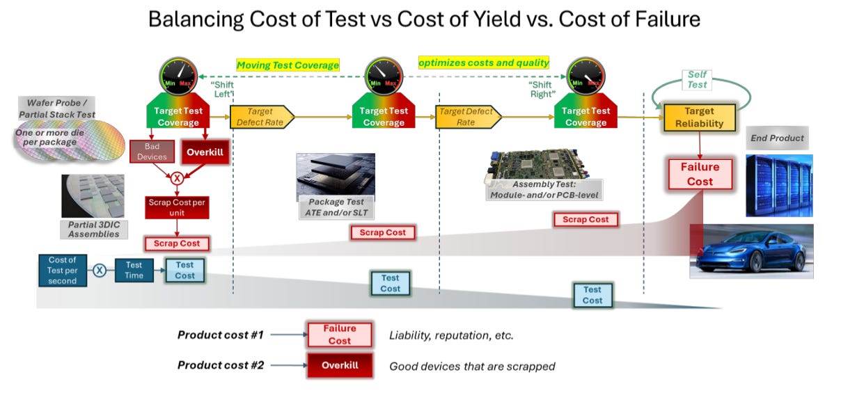
Cost-of-Test (COT) is dominated by equipment depreciation × time; the hourly cost of ATE is so high that saving even a second matters. Adding fixtures/consumables, maintenance, labor, retesting, and yield losses means that any unnecessary test step or idle time burns cash.
The first lever for capacity improvement is multi-site parallelism and resource sharing, but ideal gains (limited by PE channels, power, cooling, handler) are eroded by station swaps, sequencing, ATU recovery time, retests, and yield-driven re-tests. Thus, station balancing, power-aware vector ordering, and soak strategy optimization are required to distribute high-power/long-recovery tests.
The second lever is Test Reduction (TR) and Adaptive Test (AT): cutting low-information items through cross-correlation and failure contribution, moving the most failure-prone “judge tests” upfront for early screening, applying dynamic guardbands and conditional triggers to skip or shorten tests within model confidence intervals, and re-invoking deep scans only on boundary cases. Safeguards—minimum coverage, periodic sampling, cross-site checks, golden sample audits—ensure shorter time does not mean lower quality.
Operational metrics matter: OEE = Availability × Performance × Quality quickly reveals whether equipment is up, running fast, and producing good units. But shop-floor intuition often relies on GUPD (Good Units Per Day): when OEE is stable but GUPD drops, yield or test time is extending; when GUPD is stable but OEE falls, downtime, switching overhead, or scheduling imbalances are to blame.
Finally, make change management institutional: program versions, de-embedding files, ATU settings, and socket lifetimes must all be under MES control; any guardband or test sequence adjustment must follow PCN and requalification. That way, cost reductions are auditable, traceable, and repeatable results—not one-off “engineering magic.”
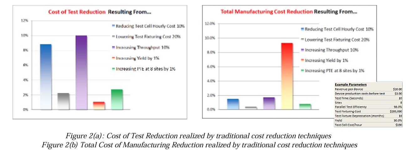
ESD/EOS, Power Sequencing, and Failure Prevention: Testing Is Not a Destructive Experiment
High-density insertions and multiple power rails magnify ESD/EOS risks severalfold. Completing HBM/CDM and JESD78 Latch-up certification before mass production is only the starting point. On the production line, the “four-piece set” of charged device control, grounding strategy, humidity management, and tooling material is required to minimize electrostatic sources. Adding discharge paths and grounding clamps around sockets/handlers helps avoid “artificial ESD events.”
For power sequencing, multi-rail products must strictly follow power-up/power-down order. ATE programs should apply controlled ramp slopes, inter-rail delays, and power-on monitoring (voltage window + current limit) to prevent undefined states that may trigger latch-up or mistakenly treat internal ESD clamps as shorts. Pre-power scanning and open-contact detection can reveal early issues such as poor contact, shorts, or socket contamination.
On protection strategies, PMU/VI paths must set hardware clamps and appropriate current compliance slew; hot-plug or transient disconnect events should trigger μs-level shutdown with fault flag logging. On the fixture side, Kelvin four-wire sensing, driver shielding, and low-leakage materials suppress false alarms.
In short, testing is not about “pushing the product until it breaks” but validating specifications and screening early failures within a safe envelope. Proper sequencing, ESD/EOS control, and protection circuitry ensure measurement results reflect the true nature of the product rather than measurement accidents.
Practical Integration of Advanced Packaging: Design—DFT—Packaging—Testing as One
In the CoWoS/SoIC era, testing must be brought to the design and packaging decision table early. At the packaging selection stage, a “testability corridor” must be planned: reserving test structures and measurement channels in the interposer, inserting IEEE 1838/IJTAG access for stacked dies, designing sacrificial pads or low-voltage probing for micro-bumps, and ensuring SI/PI and thermo–mech–electrical models share a common language from the beginning. Later, ATE de-embedding and on-die monitor readings can be cross-verified, naturally shortening bring-up cycles.
In mass production, Foundry–OSAT–ATE–Design must share the same Datasheet/Test Spec/DFT description and failure classification. All programs, de-embedding files, ATU settings, and golden samples are managed under a single source of truth (MES/PLM). Changes follow PCN and requalification processes, while CP↔FT↔SLT data lakes are correlated with WAT/inline measurements and FA results, ensuring yield and quality metrics remain consistent across sites.
When design, packaging, and testing are bound into a closed loop, the complexity of advanced packaging transforms from risk into a moat: you discover issues earlier, adjust parameters faster, deliver products more reliably, and know exactly where each second of test time should be spent.

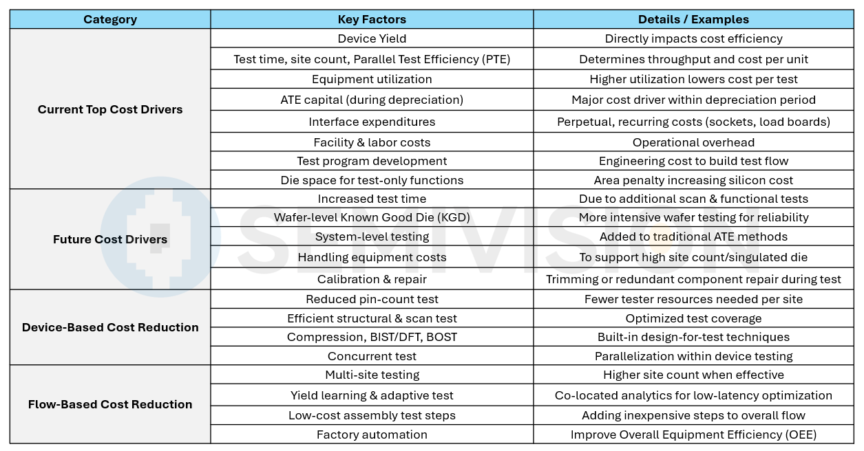


PreviousNext
TopLatestDiscussions








See all