Sailing into the AI Supercomputing Era: Key Technologies and Industry Trends at OCP APAC 2025
Sailing into the AI Supercomputing Era: Key Technologies and Industry Trends at OCP APAC 2025
- Source: SemiVision
- Author: SEMIVISION
- Published: 2025-08-17T11:02:59+08:00
- URL: https://tspasemiconductor.substack.com/p/sailing-into-the-ai-supercomputing Sailing into the AI Supercomputing Era: Key Technologies and Industry Trends at OCP APAC 2025


Sailing into the AI Supercomputing Era: Key Technologies and Industry Trends at OCP APAC 2025
Original Article By SemiVision Research (OCP,Hotchip,ECTC,Broadcom,Nvidia,AMD , Marvell ,TSMC,Nvidia,OpenAI,NTT,Meta,Google,Microsoft,ASE ,Astera Labs,ARM, MTK,Coherent,iPronics,TE,Oriole Networks)

Aug 17, 2025
∙ Paid

At a time when large language models are moving beyond the “parameter arms race,” the launch of GPT-5 has shifted the industry’s focus from “can it be done” to “is it usable, affordable, and widely applicable.” OpenAI’s key contribution lies in narrowing the gap between models and real-world workflows through engineering and product methodology. On one hand, it has chosen a favorable balance in the price–performance–reliability triangle, lowering inference costs, stabilizing long-context performance, and reducing hallucination rates—thus improving the success rate and consistency of everyday tasks such as office work, productivity, content creation, analysis, and software development.
On the other hand, it has provided developers with a more complete toolchain and runtime (spanning function calling, file/retrieval, rules and memory management, multimodal input/output, and stronger programmatic reasoning), reducing the friction of going from demo to deployment to a predictable level.
The result is that AI has transformed from “demonstrable features” into “deliverable products,” from point-level automation into auditable, governable, ROI-measurable workflow components—driving enterprises to embed model capabilities into sales, customer support, compliance, R&D, supply chains, and data governance.
At the same time, OpenAI is leveraging both product and distribution to convert model advantages into retention and revenue. For end users, ChatGPT serves as a “high-frequency entry point” for long-form writing, meeting notes, summarization, image interpretation, and lightweight coding assistance—aligning closely with users’ time and workflow needs.
For enterprises and developers, APIs and enterprise-grade features (permissions/auditing, data isolation, privatization, compliance options) make embedding models into existing systems more controllable, while smoothly integrating with DevOps, MLOps, and data stack toolchains. More importantly, OpenAI continues to abstract “model capabilities” into “composable abilities”: lightweight agents composed of task rules, tool use, memory, and retrieval. These can be easily deployed in CRM, knowledge bases, ticketing, and internal process automation. This “semi-automated with human oversight” form balances compliance and efficiency and diffuses more easily within large organizations. From a commercialization perspective, the pathway is clear and repeatable: high-frequency entry points drive stickiness and feedback, APIs expand the boundary, and enterprise features secure budgets and decision-making—together forming a reinforcing feedback loop.
The global application ecosystem is also maturing. On the user side, stable subscription and payment structures have emerged across writing, design, video, translation, data analysis, and programming assistance. On the enterprise side, the most resilient demand does not come from flashy features but from embedding AI into “processes with clear KPIs”—shortening support ticket resolution time, improving sales conversion, reducing R&D defect rates, or increasing efficiency in financial report review and compliance. Once the foundational model is strong enough and its cost/quality predictable, the determinant of unit economics shifts from “model benchmarks” to “scenario fit and distribution efficiency.” Whoever is closest to OS-level entry points, collaboration platforms, or content distribution hubs is best positioned to monetize compute into cash flow. This explains why the U.S. market is faster in productization: software distribution, cloud infrastructure, compliance systems, and procurement workflows are mature, lowering friction from pilot to scale. OpenAI provides the lowest-friction building blocks along this chain.
In China, due to regulatory, data boundary, and infrastructure differences, local vendors tend to focus on industry project delivery and system integration—embedding models into existing workflows. The broader lesson for global players is the same: sustainable value does not come from one-off model benchmarks, but from long-term integration into enterprise data assets and governance frameworks, producing repeatable templates through reliable delivery. In other words, regardless of market differences, sustainable AI growth comes from turning “models into components, components into workflows, and workflows into revenue.” For U.S. readers and decision-makers, the point is not short-term metrics but who can establish clear engineering and compliance paths for data governance, workflow orchestration, permissions/auditing, and hybrid cloud/on-prem deployment. OpenAI’s leadership in productization and developer ecosystems is accelerating the shift from concept to scaled reality.
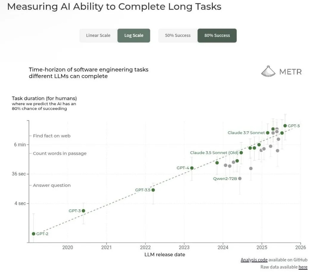
In sum, the significance of GPT-5 is not in declaring a paradigm shift but in creating a pragmatic engineering curve that links usability, affordability, and scalability into a commercial trajectory. Lower costs, better stability, more complete development/runtime capabilities, and dual push across consumer and enterprise use cases make up OpenAI’s engine for AI adoption. For enterprises and developers, the priority is no longer chasing extreme benchmarks, but embedding models into critical workflows with governance, auditing, and measurable ROI. For investors and industry observers, the next stage of defensibility lies in integrating entry points, data, and workflows into reusable, productized capabilities—where OpenAI is turning abstract intelligence into concrete business outcomes.
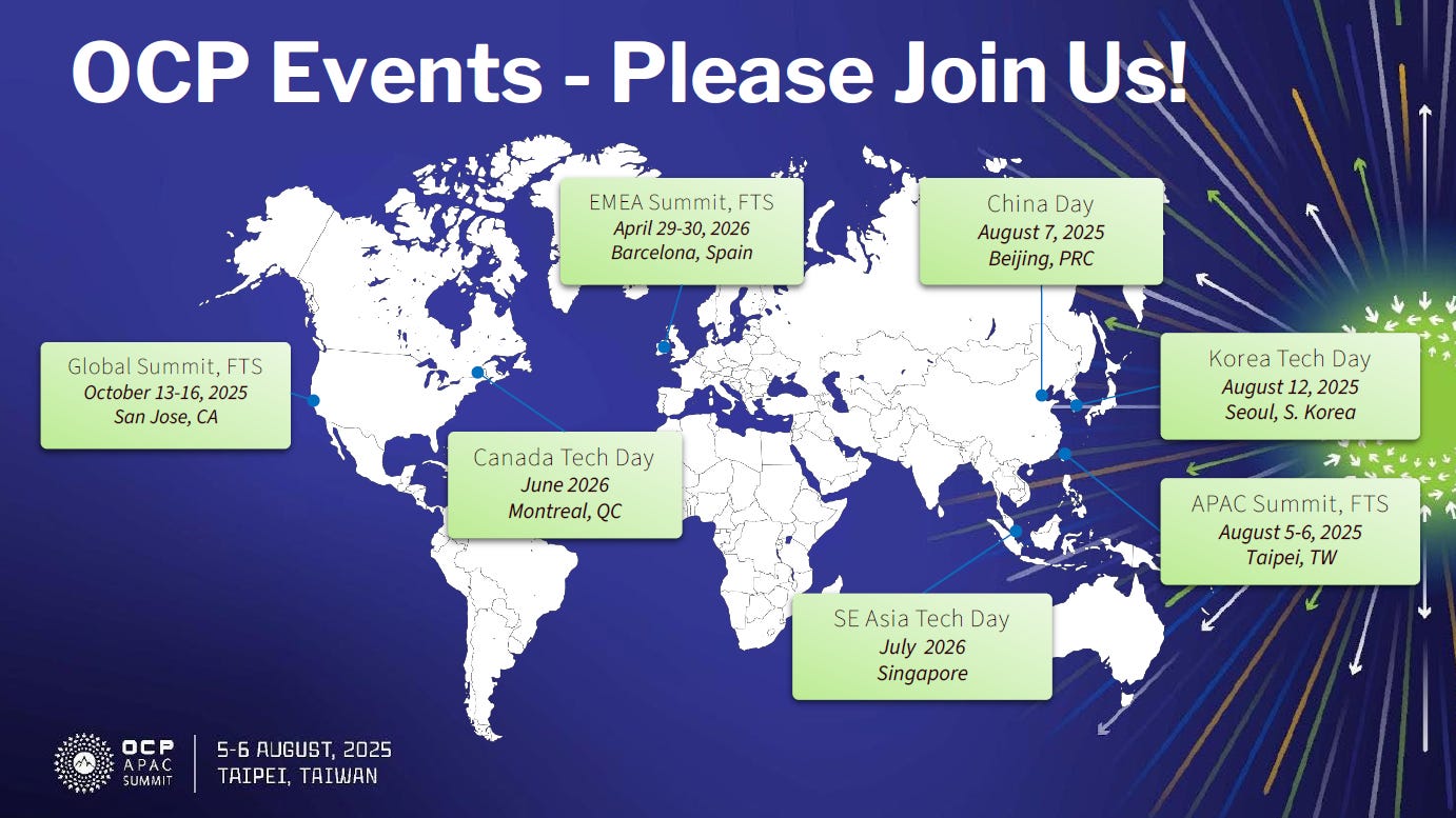
As GPT-5 shifts the industry’s focus toward usability, affordability, and scalability, what truly needs upgrading is thephysical infrastructure that carries these workflows—racks, power, cooling, networking, and sustainability. OpenAI’s product/engineering abstractions—turning models into modular capabilities embedded into governable, auditable workflows—translate on the cloud side into new workload profiles: longer contexts, higher concurrency, tighter latency/throughput coordination, and volatile cost elasticity. These constraints cannot be solved by one vendor in isolation; they are digested and standardized in the open collaboration arenas led by CSPs. This is precisely the role of theOpen Compute Project (OCP)—a pipeline that translates “model requirements” into “hardware specifications and operational conditions.” At OCP, hyperscalers like Meta, Google, Microsoft, and AWS align on cabinet power, liquid cooling, networking/acceleration, and circular storage economy through open specs and reference designs, turning hardware/software, supply chains, and operations into a common language. In 2025, OCP’s summit cadence is clear: the OCP APAC Summit in Taipei (Aug 5) and the OCP Global Summit in San Jose (Oct 13–16), the largest annual gathering for open compute, focused on pushing next-gen datacenter design toward deployable consensus.

In the AI era, several key shifts are visible along this “workflow-to-datacenter translation chain.” First, a“photonics-first” networking view: as applications move toward long-context multi-agent coordination, trade-offs across CXL/PCIe domain architectures and Ethernet/InfiniBand must balance power, latency, and maintainability. OCP’s recent educational activities on Co-Packaged Optics (CPO) reliability reflect the effort to shrink the gap between technical feasibility and scale feasibility by integrating modules, cooling, power, and testing into unified design units. Second,liquid cooling as mainstream grammar: from rack-level to campus-level cooling, standard interfaces, maintenance flows, and safety compliance need community-driven definition, or TCO and safety will fragment. Third,sustainability as a native feature: from green concrete to disk recycling and carbon label standardization, OCP embeds ESG into hardware lifecycles, making procurement, deployment, and recycling auditable. These three strands converge at OCP’s conferences, working groups, and contribution databases into replicable industrial rhythms: open specs → reference designs → testing methods → supply chain recipes.
Viewed this way, OpenAI is operationalizing the growth engine of “model capability → productization → workflows,” while OCP flattens the supply curve of “racks → datacenters → campuses.” The former defines the demand function for compute and software applications; the latter decomposes that demand into standardized, auditable, deployable industrial components. The implications for participants are concrete: software/application teams should translate SLA and latency/concurrency models into explicit networking/cooling targets aligned with OCP standards; component, system, and materials suppliers should time product definitions and roadmaps to OCP events (absorbing local CSP needs at APAC, aligning with global standards at the Global Summit); operations and ESG teams should embed sustainability and recycling into early procurement/design stages. From this vantage point, AI “scalable deployment” is no longer a vendor’s point solution but a chainwide collaboration model: workflows defined by OpenAI, translated into deployable standards via CSP–OCP coordination. For U.S. readers and decision-makers, the strategy is clear: align product and roadmap with OCP’s cadence and language, trading lower friction for faster deployment and stronger unit economics in the next wave of AI commercialization.
(Note: OCP APAC Summit will be held Aug 5, 2025, in Taipei; OCP Global Summit will take place Oct 13–16, 2025, at the San Jose Convention Center.)
The 2025 APAC OCP event has concluded, marking another highly rewarding and important forum. SemiVision has summarized some key takeaways from this year’s forum. The OCP Forum stands out as an innovative, cross-disciplinary platform, and serves as an excellent opportunity for professionals in the semiconductor industry to recharge their technical knowledge. Next on the calendar isHot Chips, which is another highly significant event.

2025年8月7日
First, we observed that OCP’s scope has expanded beyond racks, now covering AI chips, CoWoS, and CPO technologies.
At the same time,NTT Deviceshared extensive insights into silicon photonics technology, while theIWON Forumexplored the concept of an All-Optics Network. We also noted active discussions aroundOCS, with OCP now including it as a planned project.
In previous articles, we have covered numerous forums and papers fromECTC. The call for papers forECTC 2026will open soon. Looking ahead, the major events for 2025 will beHot Chips,Semicon Taiwan,IEDM, andECOC.
Hot Chips 2025
Website:https://hotchips.org/
Hot Chips 2025 will be held Sunday, August 24 - Tuesday, August 26, 2025 at Memorial Auditorium, Stanford, Palo Alto, CA.

The 2026IEEE Electronic Components and Technology Conference (ECTC), the premier technical conference and product exhibition for the world’s semiconductor packaging industry, has announced a Call for Papers. ECTC 2026 will take place May 26-29, 2026 at theJW Marriott & Ritz-Carlton Grande Lakes Resortin Orlando, FL. More than 2,000 scientists, engineers and business people from more than 20 countries are expected to attend.
Abstract submission will open on August 18, 2025 and the deadline for submissions is October 6, 2025.For all details and to submit an abstract, please visit theECTC 2026 Call for Papers.
The ECTC 2026 technical program will address new developments, trends and applications for a broad range of topics, including components, materials, assembly, reliability, modeling, interconnect design and technology, device and system packaging, heterogeneous integration, chiplet architectures, hybrid bonding, WLP and PLP, fan-out and fan-in packaging, flip-chip technologies, integrated photonics and optoelectronics, LEDs, 5G, quantum computing and systems, and other emerging technologies in electronics packaging.
Applied Reliability
Assembly and Manufacturing Technology
Electrical Design and Analysis
Emerging Technologies
Interconnections
RF, High-Speed Components & Systems
Materials & Processing
Thermal/Mechanical Simulation & Characterization
Packaging Technologies
Photonics
Interactive Presentations
At the recently concluded 2025 APAC OCP Taiwan event, what unfolded was far more than a forum on “open compute”—it was a declaration of a full-stack industry transformation, spanning from racks to silicon, from fiber optics to firmware. This high-density, cross-disciplinary exchange placed AI/HPC computing topologies, optoelectronic packaging, interconnect protocols, thermal and power systems, and supply chain strategies onto the same strategic blueprint.
This was not a mere product showcase, but a deep alignment exercise among engineers, supply chain decision-makers, and system architects. Core players including Broadcom, TSMC, ASE, Meta, Astera Labs, the UALink Consortium, and NTT revealed critical design trade-offs for the next generation of computing infrastructure—ranging from Scale-up versus Scale-out topology choices, to CPO and CoWoS efficiency boundaries, to deployable OCS and all-optical network solutions. More significantly, Taiwan, South Korea, and mainland China will no longer be isolated markets, but interconnected hubs within an Asia-Pacific “silicon ecosystem” — each contributing unique strengths in manufacturing density, memory modularization, and all-optical system integration.
If you want to know—
Why has OCP’s scope expanded from rack specifications to the entire silicon ecosystem?
What packaging and testing hurdles must CPO overcome to move from concept to mass production?
How Broadcom, AMD, and NVIDIA’s Scale-up and Scale-out strategies are shaping the AI factory landscape?
Whether OCS and all-optical networks will become the true inflection point for million-GPU clusters?
How Taiwan can seize a “Golden Decade” amid the supply chain tug-of-war between de-globalization and re-globalization?
This in-depth analysis takes you behind the scenes of the forum, decoding the engineering logic and industrial positioning that will define the computing landscape for the next decade. Understand this, and you’ll understand the hidden cards in the next AI infrastructure race.
In addition, when we think of Broadcom, another company that comes to mind is Marvell.
OCP (Open Compute Project) Global Summit – Marvell’s Showcase and Presentations
The OCP Global Summit is a major event for the open hardware community, held every fall in San Jose, California. Marvell frequently uses this platform to showcase its next-generation data infrastructure chips and optical modules, while also sharing its technical directions through various talks.
2024 OCP Global Summit
Exhibit and Demonstrations:
The event took place onOctober 15–17, 2024 at the San Jose Convention Center. Marvell exhibited at booth B1, featuring products such as the 1.6 Tb/s PAM4 DSP, Gen6 PCIe retimers, COLORZ® 800 ZR/ZR+ coherent modules, Orion coherent DSP, Spica and Nova PAM4 DSPs, and the Teralynx® Ethernet switch family.
Talks and Panels:
Marvell arranged multiple speaking sessions:
On October 15, thekeynote panel “Scaling AI Clusters: Interconnects and Memory”featured Nigel Alvares, VP of Strategy.
Khurram Malik discussed the challenges and opportunities ofStructera CXL memory devices; Venu Balasubramonian explored AI and cloud DSPs at the expo floor; Nick Kucharewski moderated theOpen Networking Switchesbreakout.
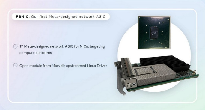
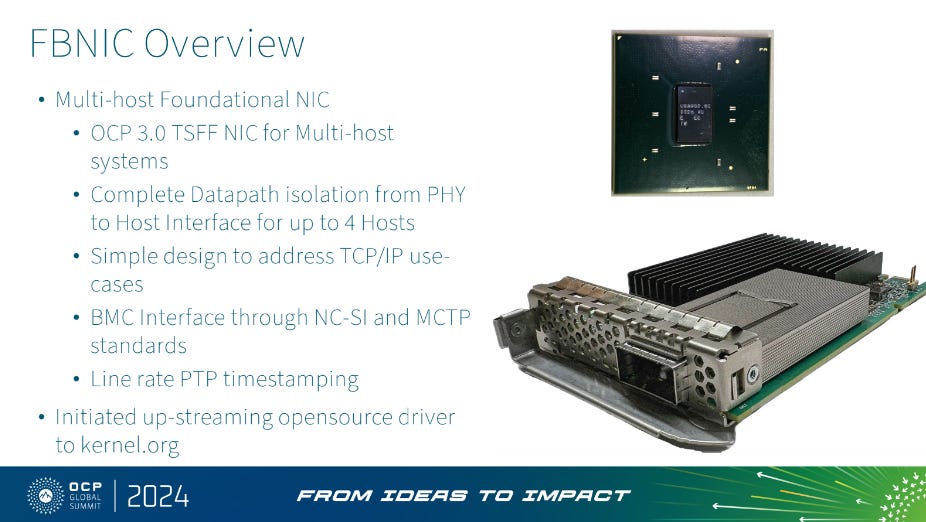
On October 16, several panels included: Jack Harwood joining theAI/HPC Future Connectivitysession to discuss the role of CXL and PCIe in AI networking; Dr. Loi Nguyen participating in anindustry panel on the right path to AI interconnects; Meta’s Dave Fenton presentingFBNIC – Meta’s control plane; plus amulti-vendor AI systemspanel.
On October 17, Marvell researchers presented topics such asusing CXL for near-memory accelerators to overcome the memory wall.
Marvell’s SerDes Optical Engines and Design Services
2025年7月8日

2025年8月4日
3D SiPho Optical Engine and Photonic Packaging
3D SiPho Optical Engine:At OFC 2024, Marvell showcased the industry’s first3D Silicon Photonics (3D SiPho) engineintegrating 32 × 200 Gb/s electrical/optical channels into a single device. Using 3D packaging, the engine combines hundreds of components—waveguides, modulators, photodetectors, modulator drivers, transimpedance amplifiers, microcontrollers, and other passive devices—into a unified package. It delivers2× bandwidth, 2× I/O density, and ~30% lower power consumptioncompared to 100G-class electro-optical solutions. The 3D SiPho optical engine can be deployed in pluggable modules or futureco-packaged optics (CPO), addressing AI datacenters’ demand for high-bandwidth, low-power optical interconnects.
Co-Packaged Optics (CPO) Architecture:In January 2025, Marvell announced its CPO architecture, which places the 3D SiPho optical engine alongside customers’ AI accelerators (XPUs), HBM chips, and other components on the same substrate. By integrating optics directly within the XPU package via high-speed SerDes and die-to-die interfaces, the design eliminates long-reach electrical traces,boosting XPU-to-XPU link rate and distance by up to 100× versus cables, while reducing latency and power. Combined with Marvell’s 6.4 Tb/s 3D SiPho engine, the CPO architecture delivers32 × 200 Gb/s electro-optical channelsin a single device, enabling high-speed optical interconnects for large-scale AI servers.
SerDes IP and Optical Engine Design Services

Marvell’s custom ASIC platform provides a rich IP portfolio and design services for building cloud and AI infrastructure chips:
High-Speed SerDes and Interconnect IP:At 3nm, Marvell offers IP blocks such as 112G XSR SerDes, long-reach SerDes, PCIe Gen6/CXL 3.0 SerDes, and240 Tb/s parallel die-to-die interconnects. These IPs support all packaging options and are deployed in Teralynx® switches, PAM4 and coherent DSPs, Alaska® Ethernet PHYs, OCTEON® processors, Bravera™ storage controllers, and custom ASICs.
SerDes Optical Engine Design Services:Marvell’s IP portfolio includes112G XSR and 224G SerDes, PCIe Gen6/CXL 3.0 SerDes, 240 Tb/s die-to-die interconnects, ARM SoC subsystems, and low-cost packaging options. These enable performance, power, and area optimization for customer ASICs. Its mixed-signal SerDes IP supports1 Gbps to >112 Gbps, covering Ethernet, PCIe, SAS, SATA, and more. Combined with 3D SiPho engines, these IPs can powerpluggable modules, co-packaged optics, and chiplet interconnects.
UALink Scale-Up Solution:In June 2025, Marvell introduced its proprietaryUALink scale-up solution, integrating 224 Gb/s SerDes, UALink PHY IP, configurable controller IP, scalable low-latency switch fabrics, and packaging options supporting both co-packaged copper and optics. This enableslow-latency, scalable interconnectsacross hundreds to thousands of AI accelerators, complementing Marvell’s custom silicon to build high-performance AI clusters.
- Collaboration with AWS
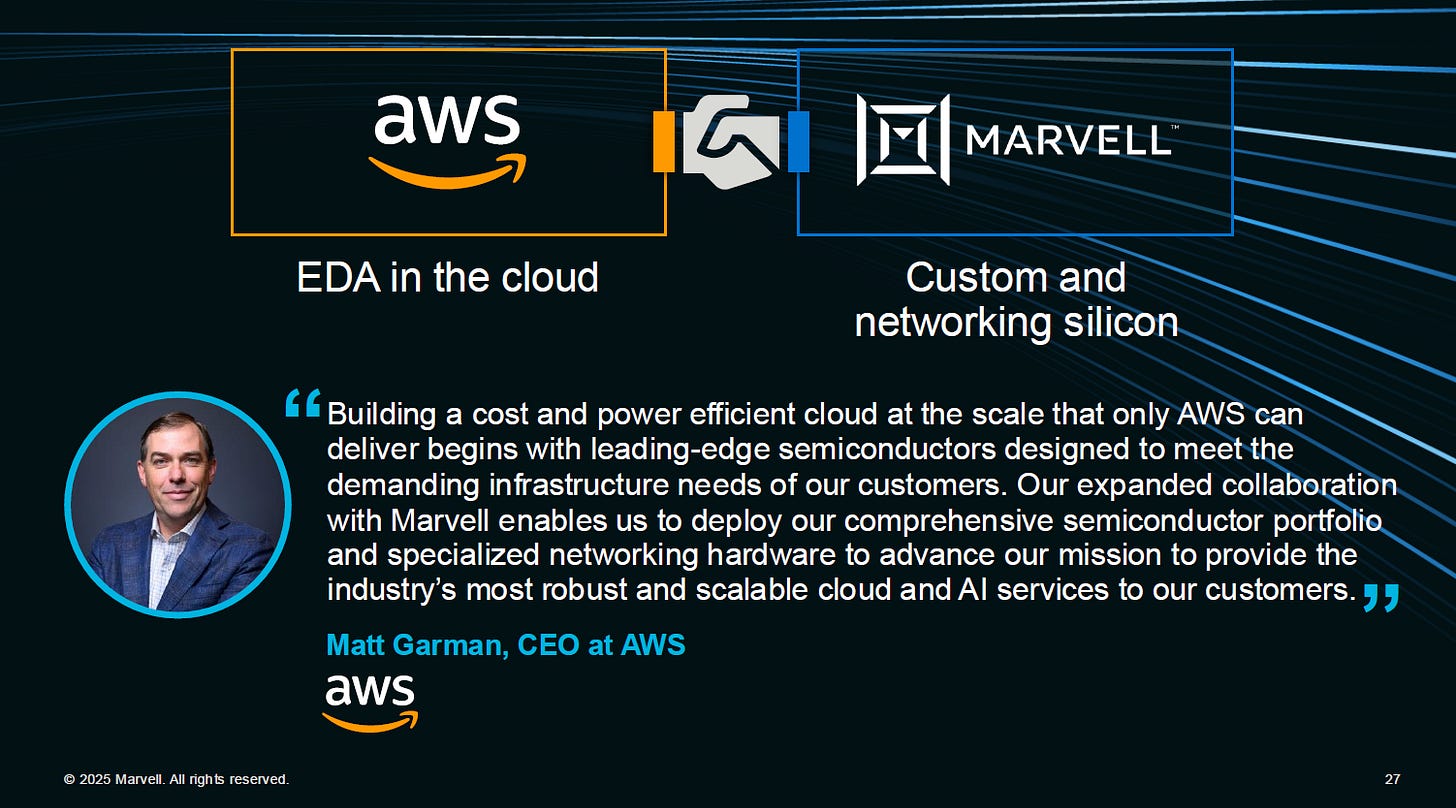
In December 2024, Marvell announced an expanded strategic partnership with Amazon Web Services (AWS):
Supply Scope:Over the next five years, Marvell will provide AWS with a broad range of datacenter semiconductors, includingcustom AI silicon, optical DSPs, active cable (AEC) DSPs, PCIe retimers, datacenter optical modules, and Ethernet switch chips.
Cloud Design Services:AWS will provide cloud-based EDA infrastructure to Marvell, enabling large-scale parallelization of silicon design workloads on AWS, shortening design cycles, and dynamically scaling compute resources.
Executive Perspectives:Marvell CEO Matt Murphy noted that AWS’s EDA infrastructure provides Marvell with dynamic design scalability. AWS CEO Matt Garman stated that Marvell’s semiconductor technologies will enhance theefficiency of AWS’s cloud and AI services, lowering TCO and accelerating time-to-market. This partnership strengthens AWS’s deployment of advanced networking and storage solutions while giving Marvell greater design flexibility.

Marvell at the OCP Global Summit
Since 2022, Marvell has actively participated in theOCP Global Summitat the San Jose Convention Center, presenting its cloud and AI infrastructure portfolio. The company has highlighted1.6T PAM4 DSPs, CXL memory devices, co-packaged optics, and switching/optical modules, collaborating with partners like Arm and Microsoft to demonstrate interconnect and optoelectronic conversion technologies. The2025 OCP Global Summit, themed“Leading the Future of AI”, will again take place in San Jose.
Hot Chips 2025 Keynote Speaker
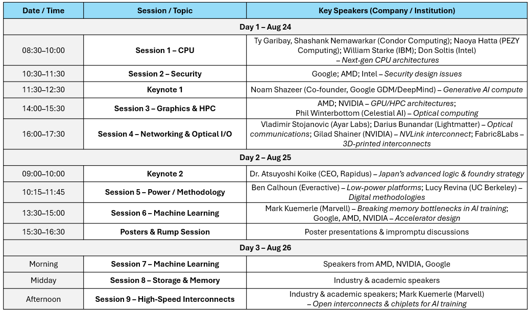
AtHC37 (Hot Chips 2025), which focuses on CPUs, optical communications, machine learning, and security, Marvell’sMark Kuemerlewill join thought leaders such as Google DeepMind co-founderNoam Shazeerand Rapidus CEODr. Atsuyoshi Koiketo present the future of AI hardware and interconnect innovation.
Marvell is aggressively leveraging itshigh-speed SerDes, 3D SiPho optical engines, and custom design servicesto advance innovation in cloud and AI datacenters. Throughcollaborations with AWS and contributions to the OCP community, Marvell is accelerating the growth of the open hardware ecosystem and driving the next wave of AI-scale infrastructure.
For Paid Members , SemiVision will discuss topics on
OCP’s Shift from “Racks” to the “Silicon Ecosystem”
Broadcom : Dual-Engine Compute Architecture: The Engineering Logic of Scale-up and Scale-out
AMD : Open Standards and Interoperability: Dual-Track Strategy of UALink × UEC
Broadcom’s Ethernet Approach: Tomahawk Ultra and AI Fabric Router
Advanced Packaging × Optoelectronic Integration: TSMC’s CoWoS + COUPE
OSAT and Modularization: ASE’s Panel and CoPoS Strategy
OCS and All-Optical Networks: From Data Center Cabling to Campus-Orchestration
NTT IOWN and the All-Optical Network
China’s dOCS and Supernode Solutions
Astera Labs:Interconnect, Memory, and Storage: PCIe Gen6, CXL3, and Gearbox
Key Factors to Watch in Semiconductor Technology
OCP’s Shift from “Racks” to the “Silicon Ecosystem”
The OCP 2025 APAC Summit in Taiwan revealed a clear and decisive transformation: discussions have moved beyond racks, data centers, and server specifications, directly targeting anend-to-end silicon ecosystemthat spans chips → packaging → optical interconnects → networking → thermal → power → firmware → operations. Representatives from Meta, Broadcom, Astera Labs, TSMC, ASE, the UALink Consortium, Digitimes, and others painted a multi-layered and actionable vision around AI/HPC computing topologies (scale-up/scale-out), open interconnects and protocols (UALink, UEC), advanced packaging and optoelectronic integration (CPO, COUPE, CoWoS), storage and memory pooling (PCIe Gen6, CXL3), total cost of ownership (TCO) for liquid cooling, system resilience and security design, and supply chain restructuring.
OCP 2025 APAC Summitshifts its focus from traditional server and rack specifications toward a fully integratedSilicon-to-Systemend-to-end engineering approach:
Interconnect Layer– Using Ethernet/UEC (Scale-out) and UALink (Scale-up) as open backbones, benchmarked against NVLink/NVLink Fusion, AWS NeuronLink, and Broadcom SUE to evaluate trade-offs between performance and openness.
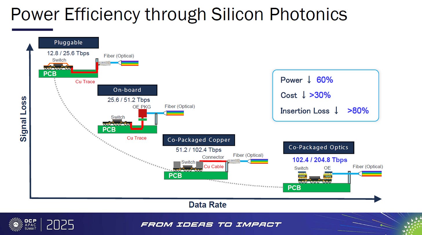
Packaging/Optoelectronics Layer– TSMC leverages CoWoS (S/R/L) together with its COUPE photonic engine to bring CPO from concept to production engineering, achieving optical I/O energy efficiency in the range of 2–5 pJ/bit.
Data Center Networking Layer–Broadcom’sTomahawk Ultra / TH6100 Tbps-class switches andAI Fabric Routerflatten and encrypt topologies from single racks to cross–data center interconnects.
Thermal/Power Layer–Direct-to-Chip (D2C)andimmersion cooling,800V high-voltage power distribution, andVertical Busbar Power (VBP)are deployed to optimize TCO for high power density AI racks.
All-Optical / OCS Layer– Real-world deployments fromGoogle, commercial products fromCoherent/Lumentum,NTT IOWN, and China’sdOCS supernode solutionsare driving the rollout of All-Optical Networks.
Supply Chain Layer– According toDigitimes, “de-globalization” and “re-globalization” are occurring in parallel. Taiwan, with its manufacturing density and modularization/packaging expertise, has become a key hub in the APAC ecosystem.
Broadcom : Dual-Engine Compute Architecture: The Engineering Logic of Scale-up and Scale-out
Core Drivers
The rise of large language models and multi-step reasoning has elevated the importance ofinter-node communication: raw compute power is no longer isolated—the true upper bound of cluster efficiency is now dictated bybandwidth, latency, consistency, and topology. Meta noted that cross-region and cross–data center training will become the norm, meaning the shift from intra-board and intra-rack (scale-up) to inter-rack and inter–data center (scale-out) collaboration is now inevitable.
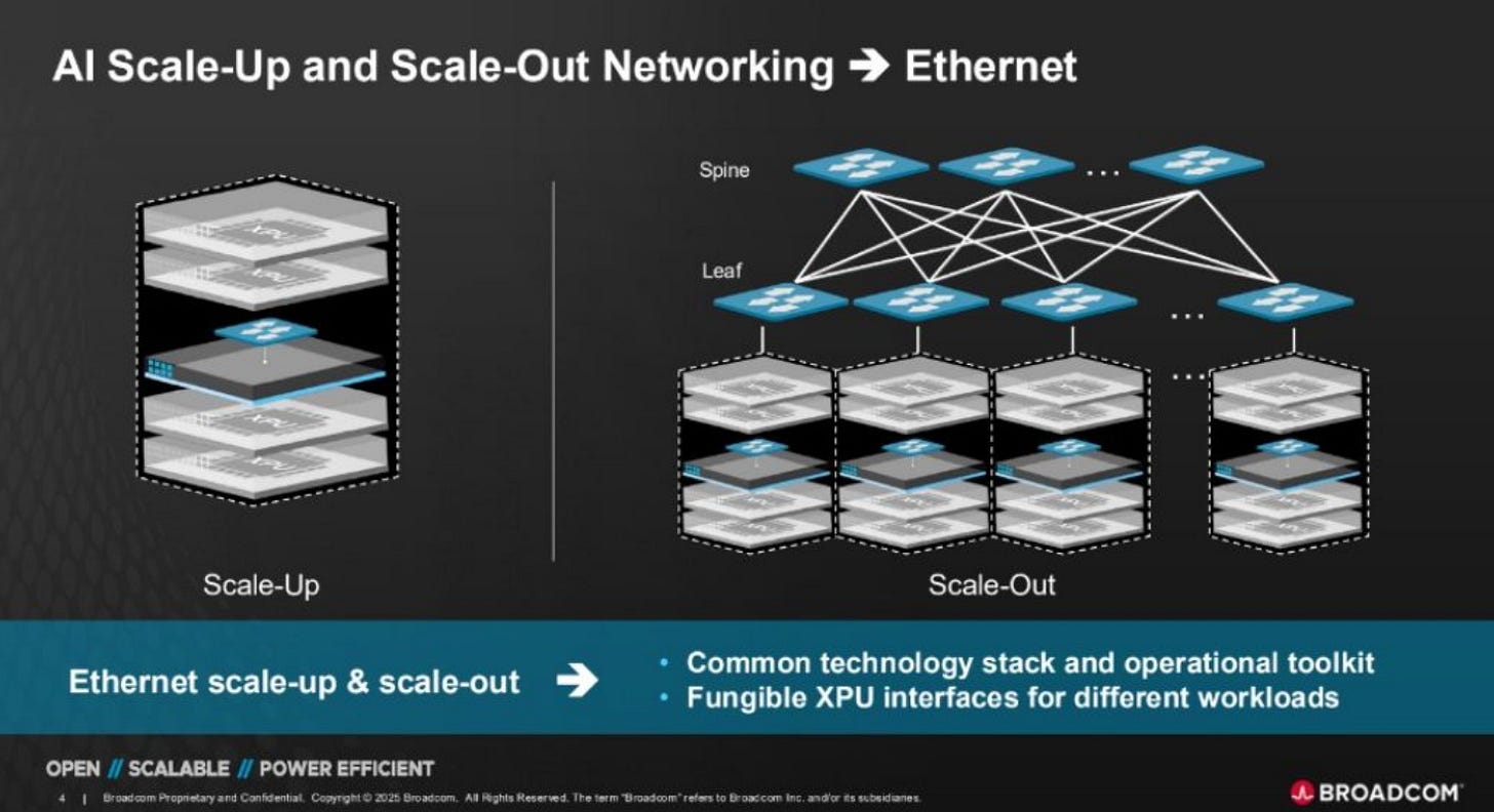
Broadcom uses theCompute–Memory–Networking triangleas its calibration axis, aligning with the architectural transition fromracktosilicon: with exploding model sizes (parameter count, context length, sequence depth) and data throughput, bottlenecks have moved from single-node compute to inter-node bandwidth, latency, consistency, and topology.
Scale-upleverages shared memory and low-latency interconnects to reduce data replication and synchronization overhead, ideal for tightly synchronized training and real-time inference.
Scale-outrelies on flatter network topologies and higher line rates to expand cluster scale, enabling large-scale distributed training and batch inference.
Ultimately,hybrid topologieswith workload-driven orchestration achieve “flexible optimal fit,” co-optimizing power, cost, latency, and scalability—where the design metric is no longer single-node TOPS, but the balanced optimum of compute, memory, and networking.
AMD : Open Standards and Interoperability: Dual-Track Strategy of UALink × UEC
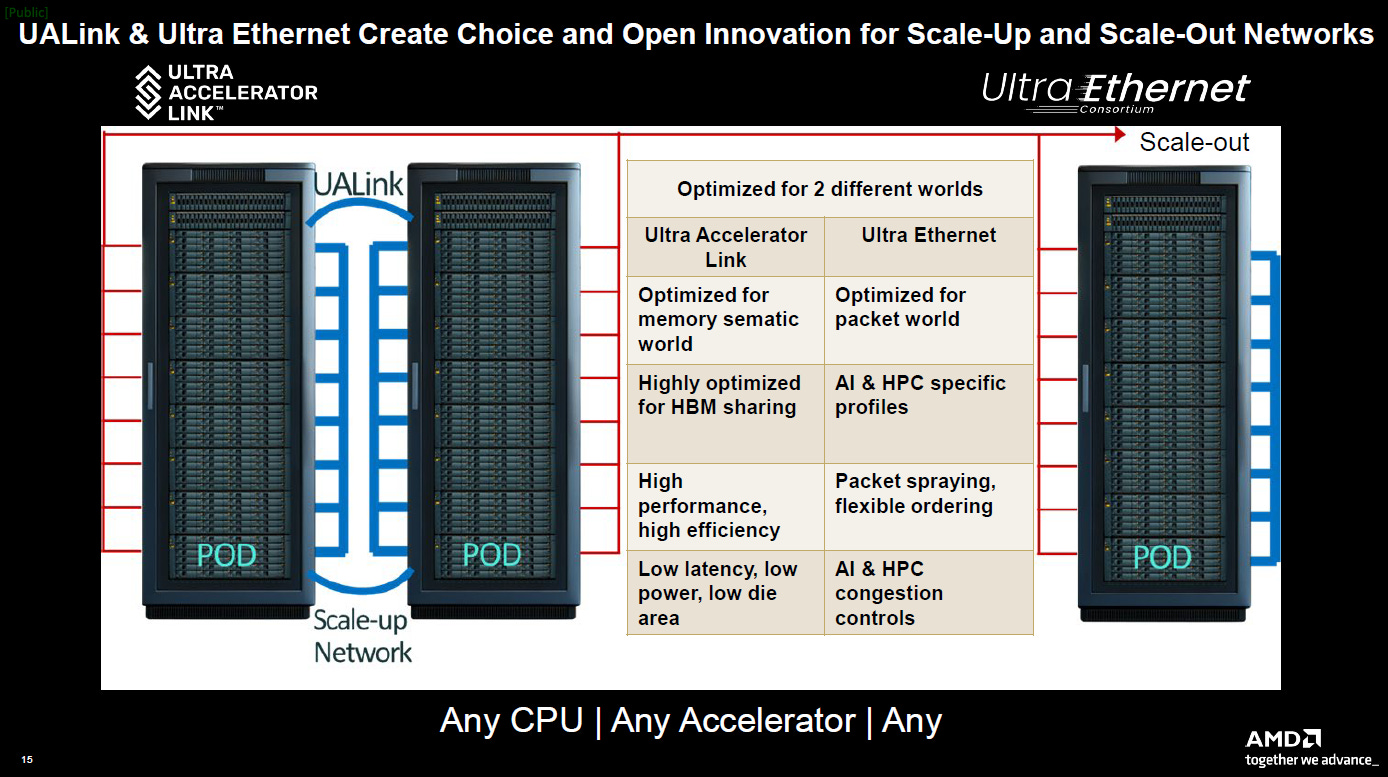
UALink (Scale-up Fabric)
Objective: Implement open-standard, low-latency/high-efficiency direct connections within accelerator domains, supporting multi-vendor CPU/GPU/ASIC and switching.
Technical Highlights: Proprietary protocol stack + IEEE 802.3 DJ 200G PHY (leveraging copper cable ecosystem), in-network collectives, chiplet I/O concepts, virtual pod partitioning, multi-vendor compatibility & certification.
Latency/Efficiency: End-to-end ~210–260 ns, bandwidth efficiency up to ~93%, far superior to conventional Ethernet stack overhead.
Variants:
UALink 200G: Targeting GPU-to-GPU high-efficiency training domains (similar to NVSwitch/NVLink scenarios).
UALink 128G (PCIe Gen7 PHY common mode): Shares frontend with PCIe7, enabling dual-mode switching for heterogeneous systems and inference consolidation.

UEC (Ultra Ethernet Consortium, Scale-out Fabric)
Ethernet excels in openness, cost curve, and operational tooling. In the 200G/400G SerDes era with flatter topologies, it leverages economies of scale to continue driving down latency and optical module costs.
Structural Complementarity: UALink (intra-domain Scale-up) × UEC/Ethernet (inter-domain Scale-out) form a layered interconnect matrix from board-level to cross–data center.
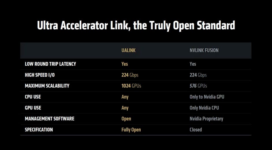
Comparison with NVLink Fusion
NVLink Fusion, under a closed full-stack model, achieves extremely high efficiency for specific combinations, but at the cost of ecosystem exclusivity and a single-track roadmap. UALink, with openness as its core, returns evolution control to the community and lowers switching costs—critical for data centers with multi-vendor, heterogeneous accelerators.
Proprietary System Comparisons
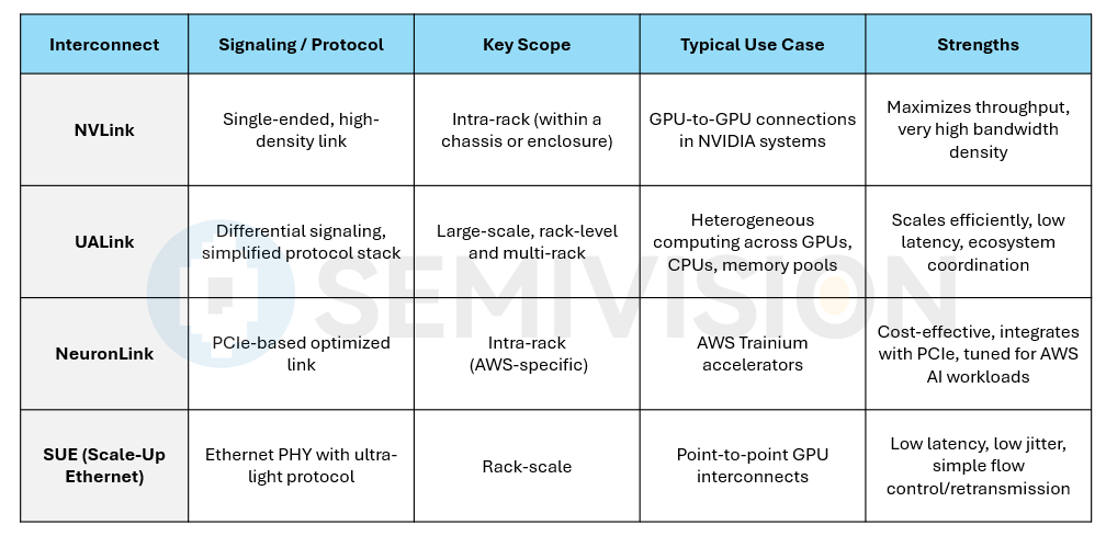
NVLink/Fusion: Excels in single-ended (GRS) signal density, extremely efficient for specific setups; constrained by closed ecosystem, node limits, and distance.
Broadcom SUE: Retains Ethernet PHY with a minimal protocol stack for efficient point-to-point; more scenario-specific and less general than UALink.
AWS NeuronLink: Deep PCIe-based optimization and overclocking with custom switches/gearboxes for AWS’s proprietary scale-up solution.

NVIDIA’sNVLink Fusiontechnology is a semi-custom interconnect platform purpose-built for future AI infrastructure, designed to enable non-NVIDIA chips—such as third-party CPUs or ASICs—to work seamlessly with NVIDIA GPUs through the NVLink high-speed interconnect architecture. Traditionally, NVLink was limited to NVIDIA’s own systems (e.g., Grace + Hopper), but the introduction of Fusion opens the door for companies like MediaTek, Marvell, and Astera Labs to integrate their own chips with NVIDIA GPUs via chiplet or chip-to-chip (C2C) connections, enabling more flexible and differentiated AI solutions. This design not only boosts bandwidth density (up to 1.8 TB/s bidirectional), but also reduces latency and power consumption, while integrating into NVIDIA’s rack-scale architecture in combination with NVLink Switch, SHARP multicast protocol, and the Mission Control automation platform to build a scalable AI compute fabric.
More importantly, NVLink Fusion is not merely a hardware interconnect standard—it is a complete ecosystem encompassing design IP, simulation tools, manufacturing support, and cloud software orchestration. NVIDIA is collaborating with Synopsys and Cadence to integrate design tools, while also partnering with server vendors, networking players (e.g., Broadcom Spectrum-X, InfiniBand), packaging providers, and chiplet technology specialists to further expand NVLink Fusion’s application scope. From AI cloud training platforms and semi-custom data center accelerators to future co-packaged optics and open-standard initiatives, NVLink Fusion positions NVIDIA as an indispensable player in next-generation AI infrastructure—establishing both a technological and ecosystem advantage over AMD’s UALink alliance.
Broadcom’s Ethernet Approach: Tomahawk Ultra and AI Fabric Router
Scale-up Metrics
Ethernet-based SU architecture targets<400 ns round-trip latency, with ~250 ns from switching and ~150 ns from uplink/downlink transmission.Tomahawk Ultracurrently delivers 50 Tbps with a roadmap to 100 Tbps, aiming to reduce network layers, fiber count, and topology complexity.
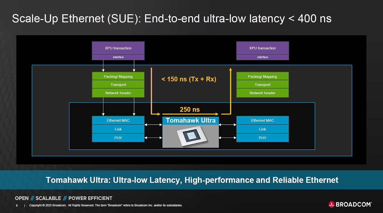
Intra–Data Center Scale-out
With 100 Tbps-class cores, the traditional three-tier topology can be collapsed into two tiers, reducing optical module needs by roughly two-thirds while improving latency and reliability. Capacity planning assumptions show feasibility for 128k–200k GPU clusters per single data center.
Inter–Data Center Scale-out
To reach million-GPU clusters, multiple 50–60 MW data centers must be woven into “geographically distributed—logically converged” superclusters. TheAI Fabric Routerhandles 60–100 km metro-scale links with deep buffering, multi-die stacking, and HBM caching, combined with line-rate encryption to ensure stable and secure inter-site data flows.
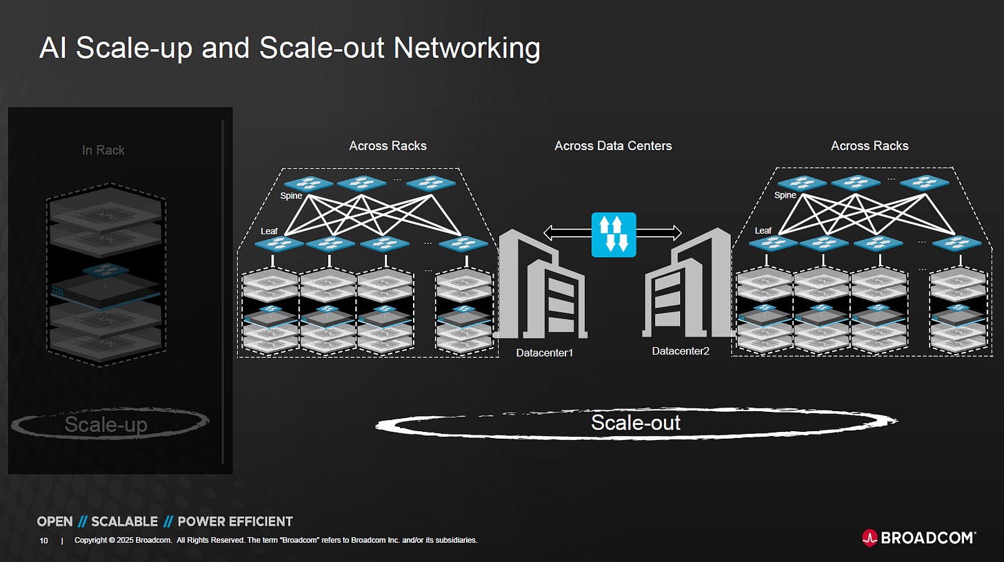
Why Ethernet
Advanced Packaging × Optoelectronic Integration: TSMC’s CoWoS + COUPE

CoWoS Evolution
TSMC’s CoWoS lineup progresses along three parallel paths—CoWoS-S(large silicon interposer),CoWoS-R(organic interposer), andCoWoS-L(hybrid type). Starting with HBM integration in 2016, it pushed interposer scaling limits by 2020 and completed the L variant in 2024. The next step is larger size, higher density, and more 3D stacking architectures, laying the foundation for CPO and ultra-high-bandwidth I/O.
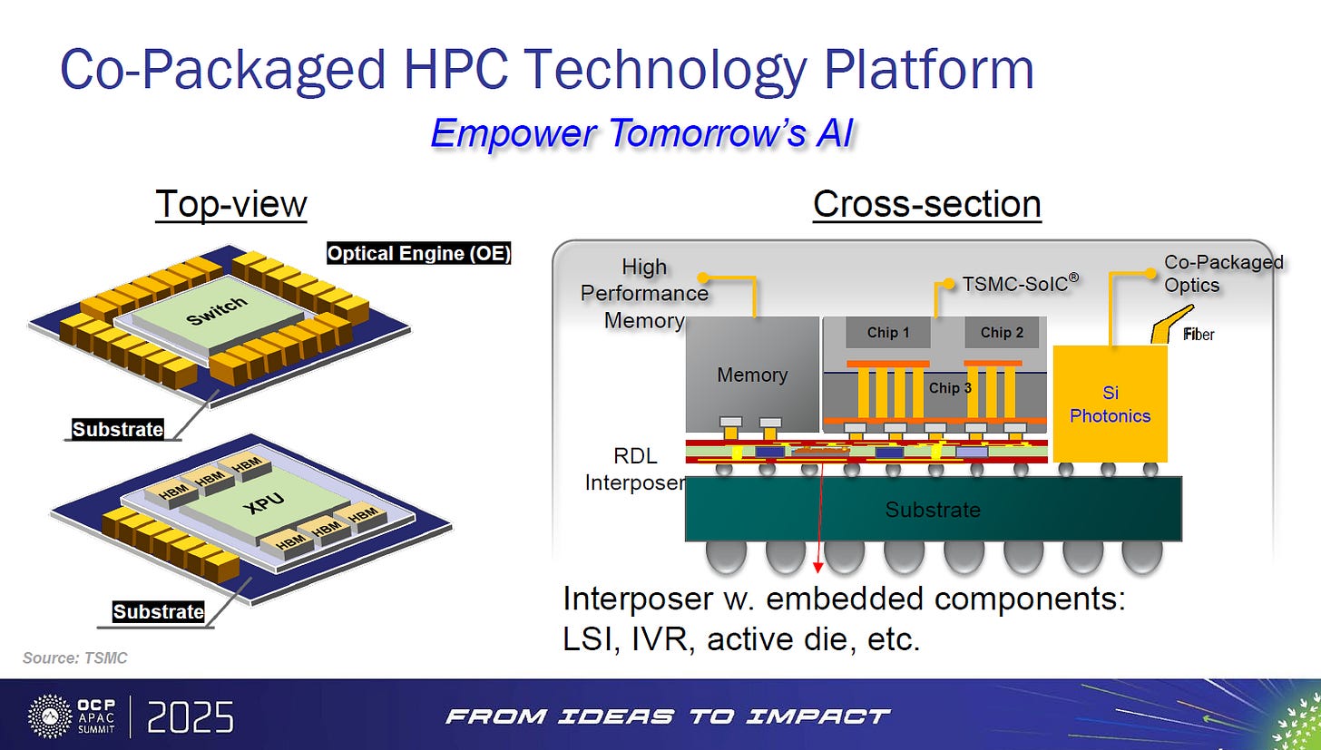
COUPE (Compact Universal Photonic Engine)
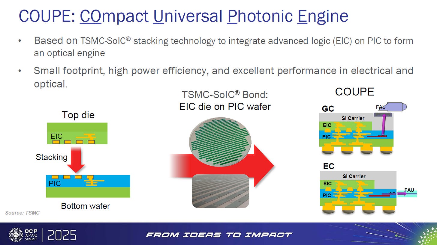
CPO System Perspective
When the photonic engine is co-packaged with the switch ASIC or compute module, SerDes trace lengths are shortened and the electrical-to-optical conversion point is moved closer to the source, reducing both I/O power and latency. CPO directly addresses the I/O wall in AI switches and HPC nodes, and its success is tightly linked with CoWoS channel density and thermal/mechanical/electrical co-design.

Mass Production Keys and Testing Bottlenecks
CP/FD testing, FAU (fiber array unit) integration, high-speed/high-yield packaging, and precision alignment automation form the “four gates” for CPO manufacturing. Without cross-domain coordination across materials, packaging, testing, and systems, achieving practical energy efficiency of 2–5 pJ/bit at stable yields will be difficult to replicate.
2025年7月16日
OSAT and Modularization: ASE’s Panel and CoPoS Strategy
ASE points to two realities: (1) AI-driven thermal and power density challenges push packaging from a device-level issue into full systems engineering; (2)Panel Level Package(including FOPLP) andCo-Packaged on Substrate(CoPoS) offer a cost/yield/modularity trade-off point. Modular heterogeneous integration (logic + photonics + memory) must be defined in concert with system architecture to ensure thermal paths, power integrity, and optical coupling aredesigned from the outsetto be manufacturable, testable, and serviceable.


2025年6月18日
OCS and All-Optical Networks: From Data Center Cabling to Campus-Orchestration
Google and OCS
Google has implemented OCS early in its data centers, using circuit-level optical switching to reduce packet congestion and retransmission overhead. Commercialization by Coherent and Lumentum indicates the supply chain is moving OCS from proof-of-concept toward productized, versioned, and mass-produced systems.
Based on current developments in Optical Circuit Switching (OCS), we observe that Nvidia is making an active push in this space. The reasons are multifaceted; however, OCS remains an emerging and innovative sector with a relatively small supplier base, and many of the challenges still tie back to fundamental architectural and operational mechanisms.
iPronicsis a technology startup originating from the Polytechnic University of Valencia, Spain. Since its founding in 2019, the company has been dedicated to the development and application of software-defined photonics, with a focus on practical OCS deployment in AI data center networks.

In March 2025, iPronics launchedONE-32, the world’s first OCS product based on silicon photonics, positioned as a large-scale optical switching engine for AI model computation and data centers. This 32-port OCS, manufactured using CMOS processes, can reconfigure links in under 300 μs while delivering near-zero latency (<30 ns). It features gain-controlled routing and bandwidth-transparent design, reducing power consumption by nearly half compared with traditional electronic packet switches (EPS) and lowering the number of required optical transceivers—significantly improving both cost and energy efficiency.

In addition, iPronics’Optical Networking Engine (ONE series)supports μs-level all-optical fast reconfiguration, O-band lossless transmission, and real-time monitoring. Leveraging its software-defined photonic integration platform, iPronics delivers ultra-low latency and highly scalable optical switching solutions—particularly suited for large-scale AI cluster low-latency communication demands.
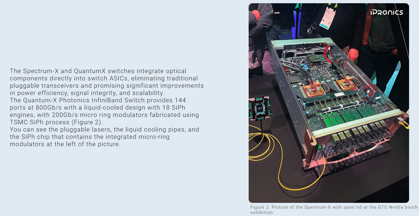
Overall, iPronics stands as one of the pioneers in nanosecond-class OCS technology. Its ONE-32 can be regarded as a commercially viable all-optical switch, laying the groundwork for OCS commercialization in intelligent computing networks and positioning itself as a driving force in the industry’s evolution toward fully optical switching architectures.
Oriole Networks, founded in 2023 and headquartered in the UK, is a startup focused on applying OCS technology to intelligent computing networks. The company has proposedPRISM, the world’s first fully optical network architecture, which utilizes AWGR-based nanosecond-class optical switching technology. PRISM is designed to replace traditional electronic switching equipment, supporting interconnection for million-scale GPU clusters while reducing energy consumption. Oriole’s approach emphasizes “plug-and-scale” expandability, and if successfully deployed, it could redefine OCS’s role in AI model training and inference networks—becoming a key enabler of fully optical intelligent computing centers.
Major OCS Suppliers and Technical Approaches
Lumentum
As a leading manufacturer of MEMS (Micro-Electro-Mechanical Systems) technology, Lumentum’s OCS solutions (such as the R300) support up to 300 input ports mapped to any output ports, offering full non-blocking connectivity, low latency, and high reliability. Leveraging decades of telecom-grade MEMS expertise, these systems eliminate OEO (optical-electrical-optical) conversions, significantly reducing both latency and power consumption, making them well-suited for large-scale AI data center deployments.
Calient
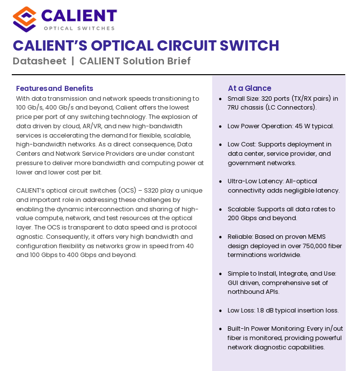
The S320 series all-optical OCS switches support up to 320 ports with port-to-port switching at latencies as low as ~30 ns, completely protocol-agnostic. Built on 3D MEMS technology, they deliver low insertion loss and high bandwidth, making them ideal for high-performance computing and data center network reconfiguration needs.
Coherent
Coherent offers OCS products designed to minimize electrical switching and OEO conversions, optimizing AI cluster network architectures for low power consumption, low cost, and low latency. While specific product details remain limited, Coherent emphasizes OCS as a key enabler for next-generation network designs.
iPronics
A startup specializing in silicon photonics (SiPh), iPronics offers OCS products such as the ONE-32, fabricated on CMOS processes, achieving nanosecond-level switching, high energy efficiency, and ultra-low latency optical-electrical switching. Active in the OCP OCS community, the company is working to extend its technology into commercially viable AI networking scenarios.
Telescent
Developer of high-capacity optical switching systems, such as the G5 fiber patch panel, capable of switching up to 16,128 fibers within a single rack. This solution targets ultra-high-density, highly automated hyperscale data center environments.
Salience Labs
Utilizing SOA (Semiconductor Optical Amplifier) technology, Salience Labs develops OCS photonic integrated circuits with high radix and low insertion loss, suitable for a range of AI network applications, including high-performance computing data centers and financial high-frequency trading environments.
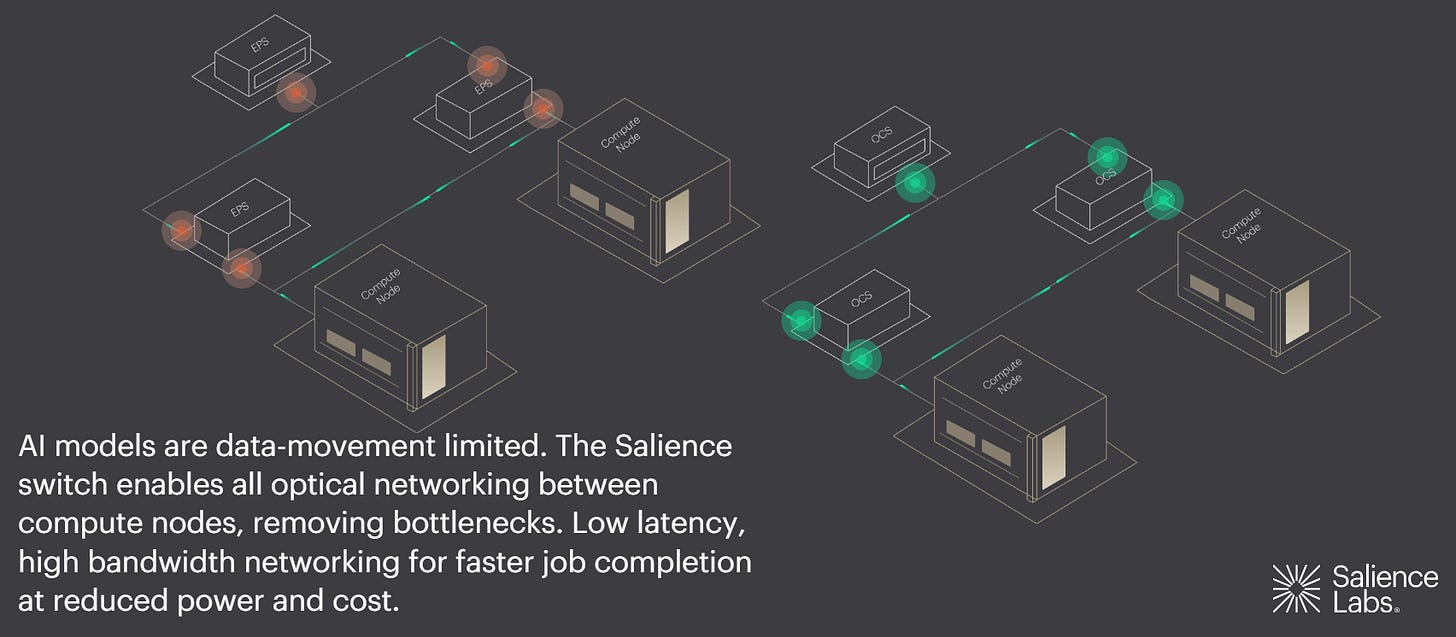
Oriole Networks
Although still in the startup phase, Oriole has proposed the PRISM all-optical OCS architecture, aiming to interconnect million-scale GPU supernodes while optimizing power consumption—positioning itself as one of the high-end nanosecond-class OCS innovators.
As an early adopter of OCS, Google has deployed OCS technology in its Jupiter and Apollo network backbones to enable optical path switching at the top-layer fabric. The company also actively promotes OCS standardization and open-source initiatives.

NTT IOWN and the All-Optical Network
IOWN’s strategy takesend-to-end latencyas the cross-domain KPI, using optical paths as much as possible from intra–data center to cross-campus connections. This makes the layer division between OCS/CPO and Ethernet/UEC clearer: optical data planes can be dynamically provisioned, while control planes run standardized packet protocols. Convergence time and reliability during topology changes become new engineering benchmarks.
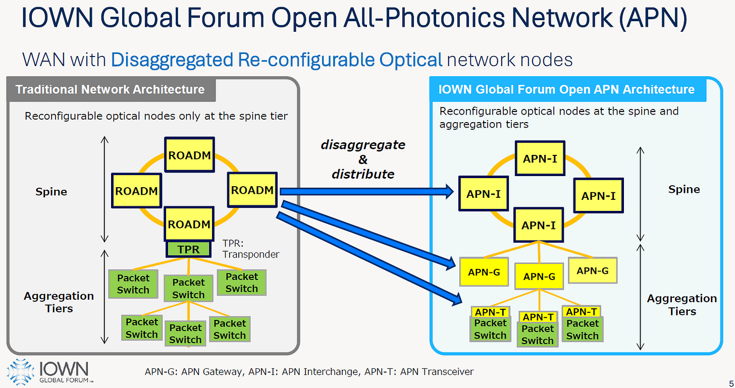
NTT Innovative Devices
In the current landscape of explosive compute demand, high-speed interconnects have become a critical constraint for both data center performance and total cost of ownership (TCO). For short distances (intra-system/intra-rack), copper cables remain dominant due to their lower per-bit energy consumption (pJ/bit) and reduced protocol overhead at sub-meter to meter ranges, offering clear advantages in energy efficiency and robustness. In contrast, Co-Packaged Optics (CPO) offers high bandwidth and low power potential, but its adoption is still in the engineering ramp-up phase due to challenges in packaging, thermal management, optical coupling, and testing. Once the optical link becomes a non-pluggable component, a single point of failure can cascade into board- or even system-level outages—one of the main reasons GPU clusters have yet to fully embrace CPO.
From a network architecture perspective,Scale-up(e.g., NVLink) prioritizes bandwidth density and strong synchronization, making it well-suited for small-scale, high-intensity training domains but limited in node count and reach.Scale-out(e.g., InfiniBand/Ethernet), while offering lower bandwidth density per link, can scale to tens of thousands of nodes, supporting large-scale distributed training and inference. In massive AllReduce scenarios, link failures can significantly amplify rollback costs. Beyond energy savings, CPO’s key value lies in reducing bit error rates (BER) and jitter, thereby improving synchronization stability.
Optical module reliability is primarily influenced by two factors:
Environmental contamination(dust, debris) affecting connector surfaces.
High temperature and thermal cyclingdegrading internal laser components.
Following the Arrhenius principle, elevated temperatures exponentially shorten laser lifespan. CPO must therefore physically isolate lasers from hot zones, employing dedicated cold plates or remote laser designs, and ensure connector designs prevent contamination ingress. While retimers can extend signal reach, they add significant power draw and thermal load; Linear-drive Pluggable Optics (LPO) eliminate the retimer but impose stricter demands on SerDes capability and link budgets. The core principle of CPO is to position the optical-electrical engine (OE) close to the ASIC to minimize electrical loss while keeping the laser operating at low temperatures.
OE integration approaches generally fall into two categories:soldered + connectorizedandsocket + pigtail. The former delivers the best energy efficiency and integration density but suffers from poor maintainability and high yield requirements. The latter supports replaceability, making it suitable for early production ramp-up and operational maintenance, but comes with higher mechanical and optical design complexity. For high-density in-rack scenarios, soldered solutions paired with remote lasers and strict inspection processes are preferred; in large-scale or edge deployments, socket-based solutions offer better maintainability.
Industry integration models are also evolving: pluggable optics provide operational flexibility but require high coordination costs; LPO increases interoperability challenges; CPO demands a redefinition of functional and reliability responsibilities between equipment vendors and operators. Hardware-software interfaces (e.g., CMIS compatibility, SDK/NOS management frameworks) must be locked in early during design to avoid becoming integration bottlenecks later.
Overall, the deployment path for CPO should follow a“short-reach copper, long-reach optical”layered strategy—addressing thermal management first, then optimizing optical path design—converting low BER and low jitter advantages into tangible system-level training efficiency gains. In the near-to-mid term, CPO is expected to roll out first at board edges, rack boundaries, and high-end switching platforms. Long term, with the maturation of remote lasers, socket-based OEs, and unified software management, CPO is poised to become the default configuration for training domains and high-bandwidth edge domains. To navigate early-stage yield and operational challenges, proactive investments in thermal management, replaceability, hardware-software interface alignment, and standardized testing processes will yield the highest return on engineering effort today.
China’s dOCS and Supernode Solutions
At WAIC, the LightSphere X architecture showcased silicon photonics–based distributed optical switching (dOCS), emphasizing pure physical-layer interconnect, switch-free topologies, and reconfigurability. Combined with liquid-cooled chiplet + CoWoS general-purpose GPU modules and domestic AI server/open platform stacks, it forms an “OCS + BR” supernode design. This strategy emphasizes supply chain security, protocol autonomy, and large-scale deployment closure.
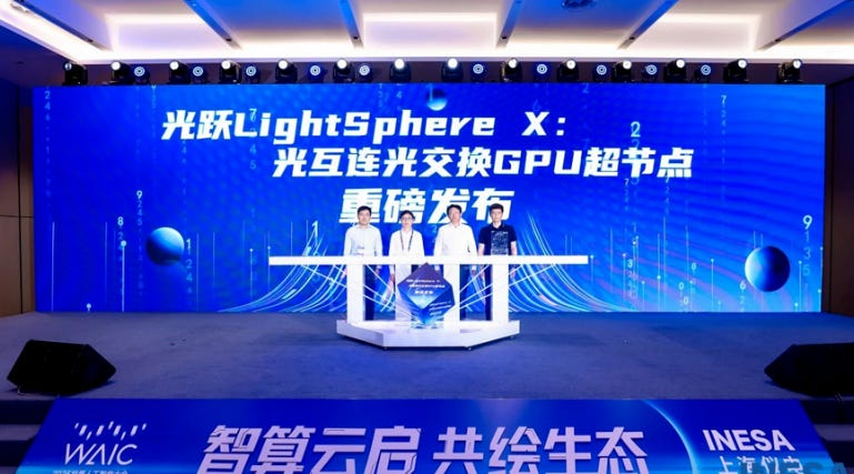
Optical Interconnect Becomes a Must-Have for Supernodes
Currently, there are two common approaches to supernode design:
Increasing the per-rack power capacity to host more GPUs. However, this is constrained by the rack-level power ceiling in data centers, limiting GPU density per rack.
Using optical interconnects to link multiple racks into a supernode, overcoming the physical limitations of traditional interconnect schemes. Compared with copper cables, optical fiber supports long-distance transmission, enabling rack decoupling from delivery constraints.
While optical interconnects offer clear advantages, they still face challenges inpower consumption, cost, and reliability. The industry is therefore moving toward more highly integrated optical products.
Pluggable Optical Modules: In this approach, the optoelectronic conversion chip is often located far from the GPU, which can impact signal integrity, increase loss, and add latency. Supernodes require not only higher per-channel bandwidth but also higher interconnect density and channel counts, driving the emergence ofNear-Packaged Optics (NPO). NPO moves the optoelectronic conversion chip from the switch to the GPU board, shortening transmission distance from 1 meter to about 10 centimeters, increasing interconnect density by 2–3×, and eliminating DSP chips — significantly reducing GPU-to-GPU communication latency. NPO is already being deployed at scale in production systems.
Co-Packaged Optics (CPO): The next core technology stage. CPO integrates the photonic engine and the compute or switching chip on the same substrate using advanced packaging techniques. Traditional optical modules connect to chips via copper traces, which are longer and more lossy. CPO shortens the electrical path from centimeters to millimeters, dramatically reducing signal loss and latency.

During WAIC 2025, Photonera Technology and Enflame Technology jointly unveiled China’s firstxPU-CPO optoelectronic co-packaged prototype system. By co-packaging the optical engine with a compute chip (xPU) directly on the substrate, the electrical distance between the electronic and photonic chips is minimized. Compared with conventional pluggable optics, this design significantly improves signal integrity, reduces loss and latency, greatly lowers system power consumption, and enhances the stability of optoelectronic conversion.
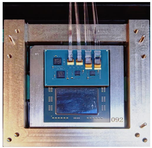
China’s first xPU-CPO optoelectronic co-packaged prototype system
iPronics Programmable Optical Switching
Programmable photonic switching turns optical routing into a software-defined network asset, allowing dynamic channel allocation within clusters across AI training phases, thereby shortening total training cycles.
Astera Labs:Interconnect, Memory, and Storage: PCIe Gen6, CXL3, and Gearbox
Astera Labs offers a deployable rack-level roadmap: PCIe Gen6 raises direct link rates to 64 GT/s, and CXL3 enables memory pooling and dynamic allocation. Demonstrations show reduced inference latency, improved GPU utilization, and better performance-per-watt. The Gearbox bridges different PCIe generations, enabling heterogeneous-generation boards to coexist and reducing asset write-offs during transition periods. With UALink carrying shared memory within accelerator domains and UEC handling large-scale east–west traffic between nodes, PCIe/CXL serves as the flexible “last mile” inside the rack.
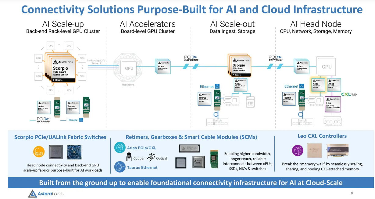
NVLink Fusion and Astera Labs Strategy
NVLink Fusion Ecosystem Membership
Following NVIDIA’s launch of the NVLink Fusion architecture at COMPUTEX 2025, Astera Labs became one of the first partners to join this ecosystem, helping to enable semi-custom AI infrastructure solutions.
Expanding Scale-Up Connectivity
Astera Labs announced that it will integrate NVLink solutions into itsIntelligent Connectivity Platform, enhancing multi-protocol interoperability across its PCIe, CXL, and Ethernet product lines combined with COSMOS software. This enables hyperscalers to rapidly deploy high-performance, low-latency deep accelerator interconnect solutions.
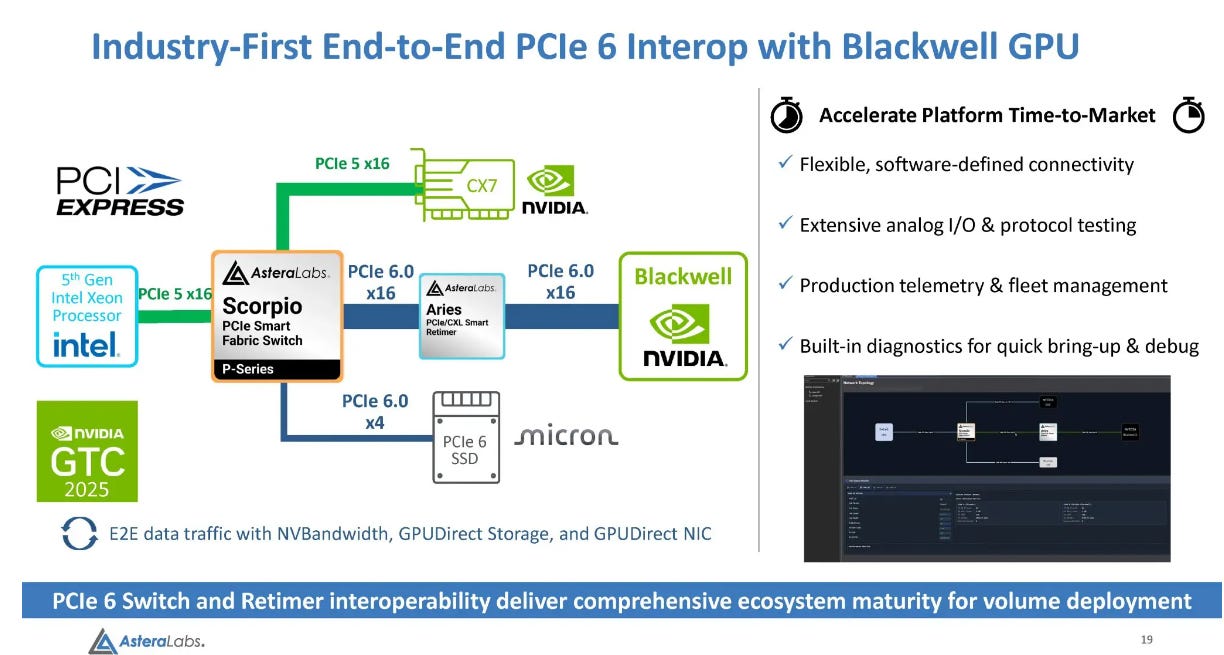
Leader in Networking and Infrastructure Innovation
Astera Labs not only continues to supply interconnect solutions for NVIDIA’s existing architectures but also actively participates in NVLink Fusion, positioning itself as a key interconnect provider for rack-scale, multi-GPU synchronized supernode networks in “AI factory” deployments.
Astera Labs, a U.S. startup specializing in PCIe retimers and switches, has in recent years focused on designing custom switch chips for cloud platforms’ AI accelerators — including the NeuronLink switch for AWS’s Trainium accelerators and the UALink switch for AMD’s MI-series GPUs.
Through its IPO and continuous product innovation, Astera Labs has rapidly risen in the AI data center interconnect space. Its involvement in the NVLink Fusion ecosystem underscores its role as a critical provider of high-speed, low-latency networking solutions, offering scalable interconnect foundations for AI infrastructure while laying the groundwork for future electro-optical convergence and scale-up network architectures.
Astera Labs and Next-Generation Scale-Up Interconnect Summary
Overview: Astera Labs specializes in PCIe retimers and switches, recently focusing on customized scale-up switch solutions for AI accelerators in cloud platforms. The company is engaged with NVIDIA’s NVLink Fusion ecosystem while also participating in AMD’s UALink and AWS’s NeuronLink initiatives.
Objective: Deliver low-latency, high-scalability intra-rack interconnect solutions for AI data centers.
Market Position: Rapidly emerging through IPO success and product innovation, Astera Labs provides the scalable interconnect foundation for AI infrastructure and plays a central role in enabling future electro-optical convergence and scale-up architectures.
NVLink (Positioning & Technology)
NVLink is NVIDIA’s high-performance interconnect designed for GPU clusters, utilizingGround-Referenced Signaling(GRS) to increase per-pin bandwidth and improve area efficiency. This design enables higher link density and total bandwidth within the same package footprint; however, single-ended signaling has weaker noise immunity and shorter distance capabilities compared to differential signaling. As a result, NVLink is primarily used for short-reach connections within a rack or chassis, while inter-rack communication relies on scale-out networks such as Ethernet or InfiniBand.
Key Figures
In the Blackwell generation, each GPU supports 18 NVLink connections, each delivering ~100 GB/s, for a total of ~1.8 TB/s (about 900 GB/s per direction).
The maximum design scale for a single NVLink domain is 576 GPUs.
UALink (Positioning & Technology)
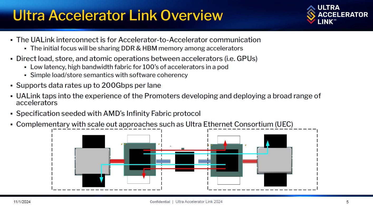
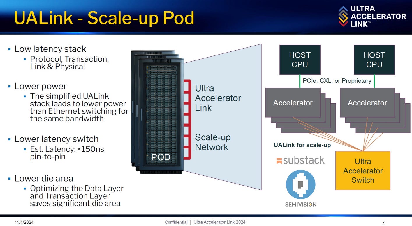
Led by AMD, UALink targets low-latency, high-bandwidth scale-up interconnects across GPUs/accelerators within a rack, emphasizing coordination with Ethernet and PCIe ecosystems. The official 1.0 specification is based on Ethernet PHY (aligned with IEEE P802.3dj), simplifying the protocol stack to reduce latency and overhead, and enabling large-scale node expansion within a singlepod.
Line rate: 200 Gb/s
Single-pod scalability target: 1,024 endpoints
The ecosystem supports two speed classes:
200G: Optimized for dense GPU-to-GPU direct connections.
128G: Believed to leverage PCIe Gen7 PHY, running the UALink protocol at the transport layer. This allows coexistence with PCIe and supports heterogeneous connections among CPUs, memory pools, and other accelerators.
NeuronLink (Positioning & Technology)
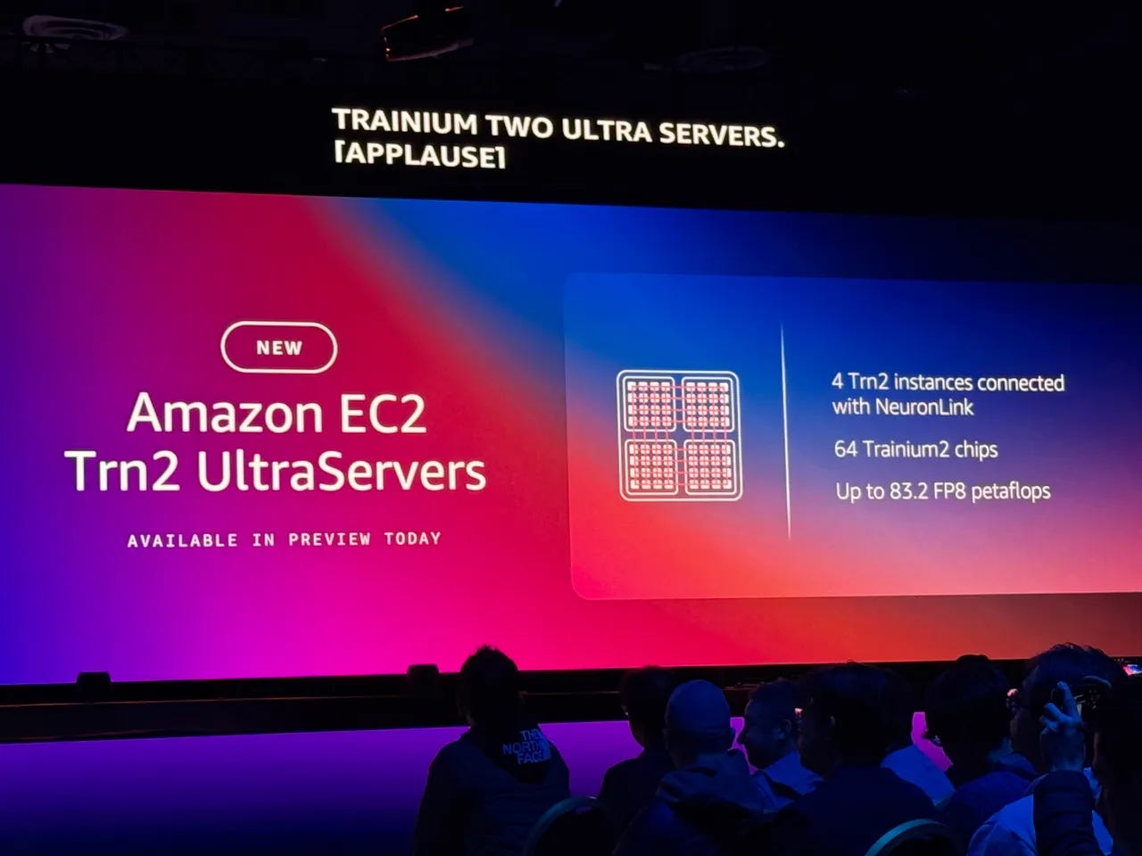
NeuronLink is AWS’s rack-scale (scale-up) interconnect for its Trainium accelerators, optimized on top of PCIe to improve packet handling and flow control for higher throughput and lower latency.
SUE (Scale-Up Ethernet)

Astera Labs Products & Platform
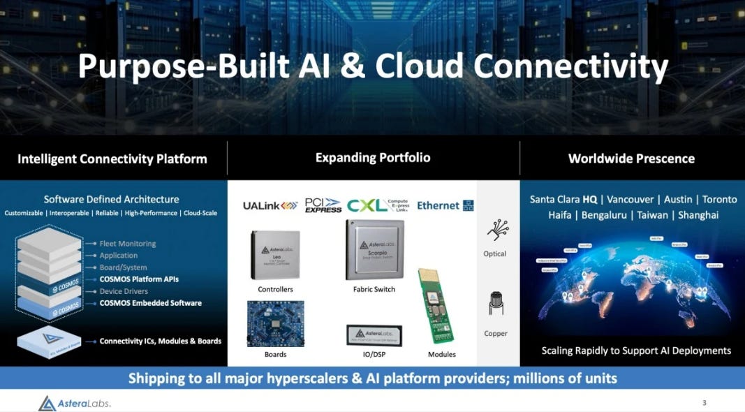
Astera Labs, through itsScorpioseries switches, offers PCIe 6/7 rack-scale switching, incorporating programmable and customizable features for large-scale customers to support NeuronLink, UALink, or pure PCIe architectures. The company is listed as an NVIDIA “NVLink Fusion” ecosystem partner, underscoring its strategic role in future GPU-to-GPU and CPU/GPU-to-Memory electro-optical convergence nodes.

AMD Helios Architecture
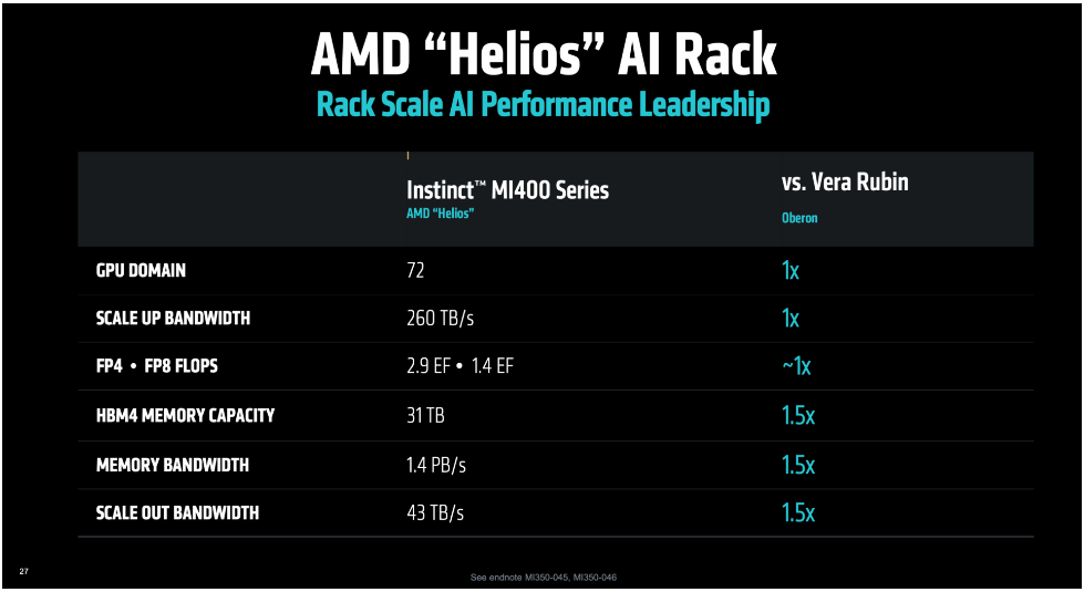
AMD has publicly disclosed thatHelios racks are built around UALink, with a design focus on72-GPU horizontal scaling.
Analytical Assumptions:
A single MI400 GPU supports72 lanes, each at25 GB/s (200 Gb/s), for atotal interconnect bandwidth of ~1,800 GB/s.
For 72 GPUs, the total switching demand is~129,600 GB/s, implying the need for12 large-scale UALink 200G switchesfor aggregation.
Cost and Market Value
A common model estimates interconnect cost as:
$/lane × lanes/GPU × number of GPUs
PCIe 6: ~$7 per lane
PCIe 7: ~$8 per lane
Smaller switches/gearboxes are priced lower
Comparative Scale:
Trainium 2.5 generation: Combined cost of large + small switches ≈$1B per million accelerators.
Trainium 3 generation: With PCIe 7 / UALink128G dual-mode, cost could rise toseveral billion USD per million accelerators.
AMD Helios: Estimated athundreds of millions USD per million GPUs.
Astera Labs, leveraging its Scorpio series and customization capabilities, spans multiple protocols and platforms, while positioning itself clearly within officially defined technical boundaries (NVLink at 1.8 TB/s and 576-GPU domains, UALink at 200 Gb/s with 1,024 endpoints, and Helios with 72 GPUs).
Thermal Management and Power: Liquid Cooling TCO, 800V Power Delivery, and Vertical Busbars
Liquid Cooling as an Imperative
Rising power density and power-per-area make it difficult for air cooling to sustain reasonable PUE and noise/maintenance costs at 30–60 kW per rack—and even more so at 100 kW+. Direct-to-chip (D2C) and single-/two-phase immersion cooling become the mainstream options, but their business viability depends on full-lifecycle TCO: upfront CAPEX, OPEX for heat exchange and cooling towers, maintenance and downtime costs, and opportunity costs from data center retrofits.
Industry Signals from Castrol
Liquid cooling is no longer just an ICT supply chain topic; with chemical, lubricant, and materials giants entering, factors such as coolant medium, compatibility, long-term stability, and regulatory compliance are being elevated to industrial-grade requirements. Castrol has announced close collaboration with major CSPs and ODMs in APAC, aiming to build a closed-loop local liquid cooling ecosystem from data center to rack to module to coolant medium—an opportunity for Taiwan’s ecosystem.
Flex’s VPD (Vertical Power Delivery)
High-voltage DC distribution and vertical busbar structures shorten high-current traces, reduce I²R losses, and lower routing complexity—paving the way for 800V architectures. Only when cooling, power distribution, and mechanical design are integrated can rack-level power, redundancy, and service windows be jointly optimized.

GIGABYTE’s ORV3 Implementation
GIGABYTE showcased ORV3-standard servers and compute nodes (including AMD CPU/GPU configurations) alongside air, liquid, and immersion cooling solutions, illustrating that a “single platform, multiple thermal strategies” approach is a pragmatic choice during the transition period, enabling modular iteration of thermal designs.

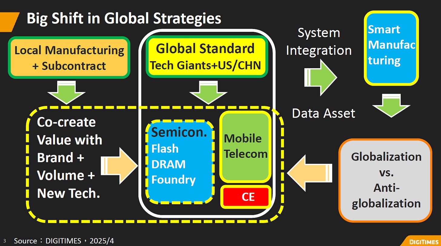
Supply Chain Restructuring: De-globalization × Re-globalization and Taiwan’s Golden Decade
According toDigitimes, three key conclusions emerge:
The supply chain is shifting fromlinear outsourcingto a parallel model ofmodularization + vertical integration. High-speed interconnect and memory pooling have become the strategic high ground for ecosystem influence.
Vietnam, Malaysia, and India are taking on new manufacturing capacity and market growth; Europe and South Asia are accelerating investment attraction; while Japan, South Korea, and Taiwan remain among the few regions with a fully integrated domestic semiconductor chain.
Taiwan enters the global market from thesupply side, complementing the U.S.’sdemand-sideentry. Through an “inside-out” alliance model, Taiwan is moving from OEM/ODM toward a new role that integrateshardware × software × platforms. This forms the industrial foundation for Taiwan’s “Golden Decade.”
System Security & Resilience: From Firmware to Cross-Campus Orchestration
Methodology: Turning “Openness” into Replicable Engineering Productivity
Topology Selection– Start by analyzing workload communication characteristics (bandwidth, burstiness, global synchronization frequency, parameter-to-server ratio) to determine the optimal scale-up/scale-out mix. Then apply UALink/UEC/Broadcom line-rate–latency–layer combinations in a two-stage optimization process.
Closed-loop Testing– Establish a mixed electro-optical test chain from CP/FD → package level → system level → SLT, incorporating data-driven yield prediction and failure traceability.
TCO Modeling– Integrate energy efficiency (pJ/bit, W/GPU), optical cost ($/Gbps), cabling density, thermal CAPEX/OPEX, power distribution losses, facility retrofitting, and downtime costs into a unified financial model to avoidlocal optima, global sub-optima.
Key Factors to Watch in Semiconductor Technology
Proven UALink × UEC interoperability and the first batch of compatibility certifications.
Commercial-scale PCIe Gen6/CXL3 deployments in data centers, and real-world Gearbox performance in mixed-generation environments.
CPO (including COUPE) high-volume manufacturing timeline, optical–electrical yield, and thermal dissipation production ramp curve.
Supply chain release points for 200G/400G SerDes Ethernet and the scale of two-tier topologies in the 100 Tbps era.
Liquid cooling medium and module standardization (including maintenance and decommissioning rules), as well as real-world 800V power distribution/VBP safety in volume racks.
OCS performance–economics–reliability verification in CSP and hyperscale private cloud orchestration.
Project milestones and supply chain alliances in Taiwan–Korea–China for CPO/OCS/ORV3/Panel/FOPLP.
Thermal technology developments, including NO TIM or Si IMC solutions.
Broadcom TH6 technology evolution.
Application of TSMC silicon photonics in AI chip integration.
ASE silicon photonics development progress.
CoPoS extensions and TGV advancements.
Samsung System-on-Panel technology progress.
Chiplet architecture evolution and heterogeneous integration.
Conclusion: An Open Order for the Silicon Ecosystem
The OCP’s first stop in Taiwan is not the end but the beginning of a closed loop linking open standards → engineering roadmaps → ecosystem assembly → business models. With UALink/UEC as the backbone, Broadcom Ethernet as the nervous system, TSMC’s CoWoS+COUPE as the joints, ASE’s modularization as the tendons, and OCS/IOWN as the circulatory system—supplemented by Castrol, Flex, and GIGABYTE in thermal–electrical–mechanical integration—the APAC silicon ecosystem is evolving from points to lines, and from lines to a mesh.
As Taiwan connects global demand through supply-side strengths, and South Korea and China contribute high-density memory and all-optical networking capabilities, the OCP’s open order can integrate the region’s multi-center advantages into a unified computing infrastructure.
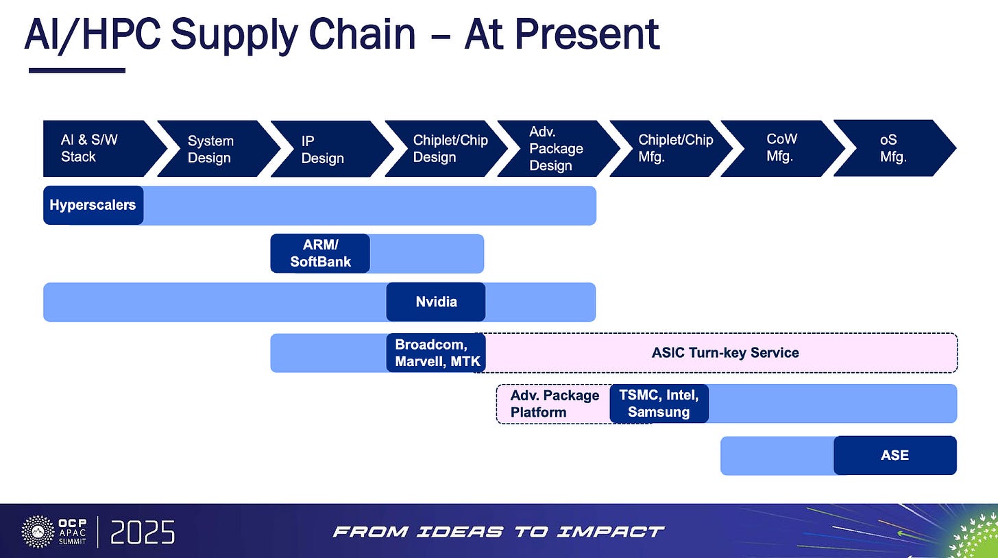
TheAI/HPC supply chain at presentshows several important shifts and inflection points:
Vertical Expansion by Hyperscalers
Hyperscalers are no longer confined to the AI/software stack. They increasingly extend their influence across system design, IP design, chiplet/chip design, and even advanced packaging. This reflects their push for end-to-end control over performance, cost, and supply resilience.
Role of ARM/SoftBank
ARM, under SoftBank, is positioned as a key IP provider, but its reach is more narrowly focused compared to hyperscalers. Its leverage is concentrated at theIP design stage, shaping architectures that downstream partners adopt.
Nvidia’s Broadened Scope
ASIC Providers as Turnkey Players
Companies likeBroadcom, Marvell, and MediaTek(MTK) operate across IP design and chiplet integration, offeringASIC turnkey services. They fill a critical role for hyperscalers and system integrators that demand custom silicon but lack in-house semiconductor design and manufacturing.
Foundry & Packaging Consolidation
Advanced packaging and manufacturing remain concentrated inTSMC, Intel, Samsung, andASE. These players provide the physical backbone—fabrication, chiplet packaging, and OS manufacturing—that underpins hyperscalers’ and fabless companies’ ambitions.
Key Inflection Point:
The major shift lies inconvergence and overlap:
Hyperscalers and Nvidia are pushing deeper into hardware territory.
ASIC service providers are bridging the gap with turnkey solutions.
Foundries and packaging firms are becoming bottlenecks and critical enablers, especially with AI/ML workloads demanding chiplet integration, high-bandwidth interconnects, and advanced packaging.
The supply chain is transitioning fromlinear specializationto aconverging ecosystem, where differentiation depends not just on technology but also on integration, partnerships, and control of bottleneck capabilities (IP, packaging, interconnect).


PreviousNext
TopLatestDiscussions








See all