Advantest Leading the AI Testing Wave: Earning the Title of the “ASML of the Test Industry”
Advantest Leading the AI Testing Wave: Earning the Title of the “ASML of the Test Industry”
- Source: SemiVision
- Author: SEMIVISION
- Published: 2025-08-10T21:16:30+08:00
- URL: https://tspasemiconductor.substack.com/p/advantest-leading-the-ai-testing Advantest Leading the AI Testing Wave: Earning the Title of the “ASML of the Test Industry”


Advantest Leading the AI Testing Wave: Earning the Title of the “ASML of the Test Industry”
Original Articles By SemiVision Research (TSMC, Nvidia , Advantest , Teredyne , Formfactor , FiconTEC , Broadcom ,Marvell , MPI)

Aug 10, 2025
∙ Paid

In the previous article, we discussed many topics related to silicon photonics, advanced packaging, CMOS scaling technology, and some testing concepts. As AI chips become increasingly complex, ensuring chip reliability presents significant challenges. We have also observed the rapid growth of the testing industry. Today, we will briefly talk about the testing leader: Advantest.

2025年4月15日
2025年7月16日

Starting with Electronic Measurement Technology: Advantest’s Growth Alongside Japan’s Electronics Industry
Our origins trace back to being a developer and manufacturer of multifunctional electronic measuring instruments, such as voltmeters and frequency counters. After achieving success in this field, we adopted an effective strategy: focusing on niche markets and leveraging advanced technology to deliver high-performance products, thereby securing market share.
As Japan’s electronics industry expanded in the late 1960s, we were among the earliest to foresee the semiconductor industry’s potential to create historic opportunities. We directed our capital investment toward developing testing systems based on our electronic measurement expertise. Overcoming management crises and other challenges, we successfully launched world-class semiconductor test systems.
Milestones
1954– Founded Takeda Riken Industry Co., Ltd.
1957– TR-124B digital frequency counter became a best-selling product.
1963– Introduced Japan’s first domestically produced digital voltmeter with a 100,000-digit display.
1972– Released Japan’s first domestically produced semiconductor test systems: T-320/20 and T-320/30.
1979– Launched the world’s highest-performance VLSI test system with a test frequency of 100 MHz.

Original workforce. Founder Ikuo Takeda is second from left in the front row.
Advantest’s Rapid Growth Alongside the Semiconductor Industry
During this era, fueled by the rise of personal computers and the emergence of the internet, the semiconductor market expanded significantly. Advantest’s semiconductor testing systems integrated cutting-edge measurement technology with high-volume manufacturing capabilities, supporting the evolution and advancement of semiconductor equipment. By 1985, the company had become a global leader in the semiconductor test equipment market, with testing systems becoming its core business.
Milestones
1982– Established a local subsidiary in the United States, later expanding manufacturing operations to other regions worldwide.
1985– Renamed asAdvantest Corporation. According to VLSIresearch (now TechInsights), the company ranked No. 1 in global market share for semiconductor test equipment.
1993– Launched the T6691, a large-scale integrated circuit test system offering industry-leading testing speeds of 500 MHz/1 GHz.
1995– Introduced the T5581, a 250 MHz S-DRAM memory test system, which became a best-selling product.

T5581, a 250 MHz S-DRAM memory test system
From expanding globally to pioneering high-speed, high-performance testing solutions, Advantest cemented its position as a driving force in advancing semiconductor testing technology.
Advantest’s Alignment with Shifts in Semiconductor Value Chains
At the turn of the 21st century, the rise of smartphones and the proliferation of personal computers became major drivers of semiconductor demand. The global distribution of semiconductor design and manufacturing advanced rapidly, creating a growing need for cost-efficient and high-performance testing. In response, Advantest worked to stabilize its business base while taking proactive, forward-looking measures, including the acquisition of overseas companies.
In 2011, Advantest acquired Verigy, marking the second time in its history that the company’s destiny hinged on a bold strategic move. This acquisition brought significant returns, as Verigy’s global customer base and operational expertise provided a strong foundation for Advantest’s growth in the years to come.
Key Milestones
2000– Selected as one of the 225 stocks comprising the Nikkei 225 Stock Average.
2001– Established Japan’s largest bio-cluster within the Gunma R&D Center.
2003– Acquired Nihon Engineering’s open architecture SoC test system T2000.
2008– Acquired Credence Systems GmbH.
2011– Acquired leading semiconductor test equipment company Verigy.
2013– Acquired W2BI.COM.
2018– Announced a mid-term business management plan with a broad, long-term vision.
2019– Acquired Astronics’ semiconductor system-level test business in the U.S.

In 2011, Advantest acquired Verigy
Through strategic acquisitions, market foresight, and continued technological innovation, Advantest has positioned itself as a global leader, ready to adapt to the evolving semiconductor value chain.
Advantest Expands Business Through Measurement Technology While Driving ESG Sustainability
Advantest anticipates that the widespread adoption of AI and 5G will trigger explosive growth in global data processing demands, ushering the semiconductor market into a new stage of development. Semiconductors play an increasingly critical role in powering today’s data-driven society, where precision, complexity, and capacity requirements continue to rise—along with the need for greater reliability.
As digital transformation accelerates and the semiconductor value chain continues to evolve and expand, Advantest remains committed to creating new value for customers. This includes broadening its business scope into system-level testing and data analytics.
Key Milestones
2020– Acquired U.S.-based Essai Inc. and formed a business alliance with PDF Solutions (U.S.); launched the V93000 EXA Scale™.
2021– Established an ESG Action Plan, announced the second Mid-Term Management Plan, and acquired U.S.-based R&D Altanova Inc.
2022– Acquired CREA S.r.l. in Italy.
2023– Acquired Taiwan-based ACE Technology Co., Ltd.

Advantest’s system-level test system R&D and manufacturing facility in the United States
With these strategic moves, Advantest strengthens its global presence while reinforcing its commitment to sustainable growth and environmental, social, and governance (ESG) principles.
Advantest Leading the AI Testing Wave: Earning the Title of the “ASML of the Test Industry”
Global Positioning and Market Leadership
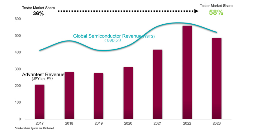
Advantest (Japan) is the world’s leading supplier of Automated Test Equipment (ATE), holding roughly 50% of the global market share in 2023, with the combined share of Advantest and the U.S. player Teradyne reaching around 80%. The company offers a comprehensive product portfolio that spans SoC, mixed-signal, and memory testers, system-level test (SLT) platforms, test handlers, and interface solutions, all integrated with edge computing and data analytics capabilities.
AI and HPC Testing Strategy
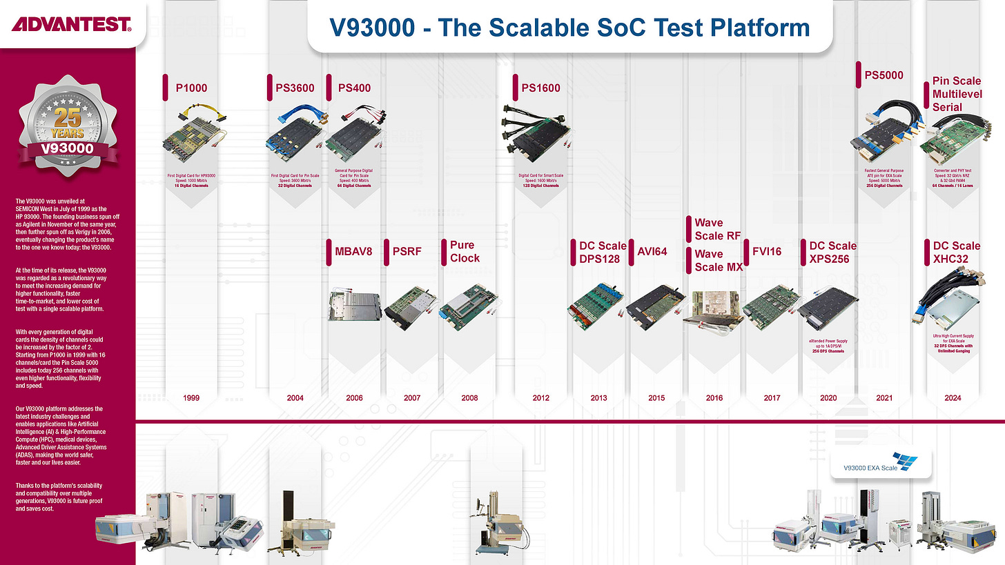
Advantest is aggressively investing in AI and high-performance computing (HPC) chip testing, recognizing that next-generation processors and accelerators demand more complex validation methodologies. Its flagship V93000 EXA Scale platform and T2000/7038 SLT series are specifically engineered to handle high current loads, high-speed serial interfaces, and advanced system-level testing. These platforms are complemented by the Advantest Cloud Solutions (ACS) ecosystem, which leverages AI and machine learning for real-time analytics and adaptive test decision-making.
Industry Impact and Technology Leadership
The company has frequently highlighted“AI chip testing”as a strategic theme at multiple international conferences, signaling its determination to lead the emerging AI/HPC testing domain. By offeringcutting-edge, highly automated, and data-driven test solutions, Advantest positions itself as the“ASML of the test industry”—an indispensable enabler for the semiconductor ecosystem, especially as AI workloads and chip complexity accelerate.

Teradyne (United States)
Holding approximately 30% of the global ATE market, Teradyne is a key competitor in semiconductor test solutions. Its core product lines include the UltraFLEX and J750 SoC test systems, as well as memory test platforms, and the company also has a presence in the industrial robotics sector.
Teradyne has expanded its capabilities in RF and system-level testing through acquisitions such as LitePoint(wireless and RF test solutions) and Eagle Test Systems (high-speed and analog test technologies). The company’s CEO has emphasized that AI chips are expected to drive revenue growth in the second half of the year, underscoring the significant impact of the AI boom on semiconductor test demand.

Cohu (United States)
Cohu focuses onpower and RF (radio frequency) testing, with its product portfolio integratingburn-in and system-level testing (SLT)capabilities through theIsland platform. The company has also beenexpanding its robotics and thermal management technologiesto meet the requirements ofpower semiconductors and AI chip testing, where precise handling and high-temperature operation are critical.
While Cohu continues to enhance its presence inspecialized and high-growth markets, itsoverall scale remains smaller than industry leaders Advantest and Teradyne, positioning it as a niche player targeting the evolving demands of AI and power semiconductor testing.

NI (National Instruments, post-merger with Texas Instruments and Emerson)
NI providesmodular and flexible test platformsthat cater to a wide range of semiconductor and electronic system validation needs. Following its2024 merger with Emerson, the company expanded its footprint into theIndustrial Internet of Things (IIoT) and edge analyticsdomains, aiming to bridge industrial automation with advanced test solutions.
In 2025, Advantest and Emerson announced a strategic collaboration to build an AI-driven test ecosystem, combining Emerson’s industrial edge computing capabilities with Advantest’s real-time data and analytics platforms. This integration is designed to enhance semiconductor test efficiency, improve yield, and enable adaptive, data-driven test workflows, reinforcing NI’s role as a key enabler in the era of AI-powered semiconductor manufacturing.
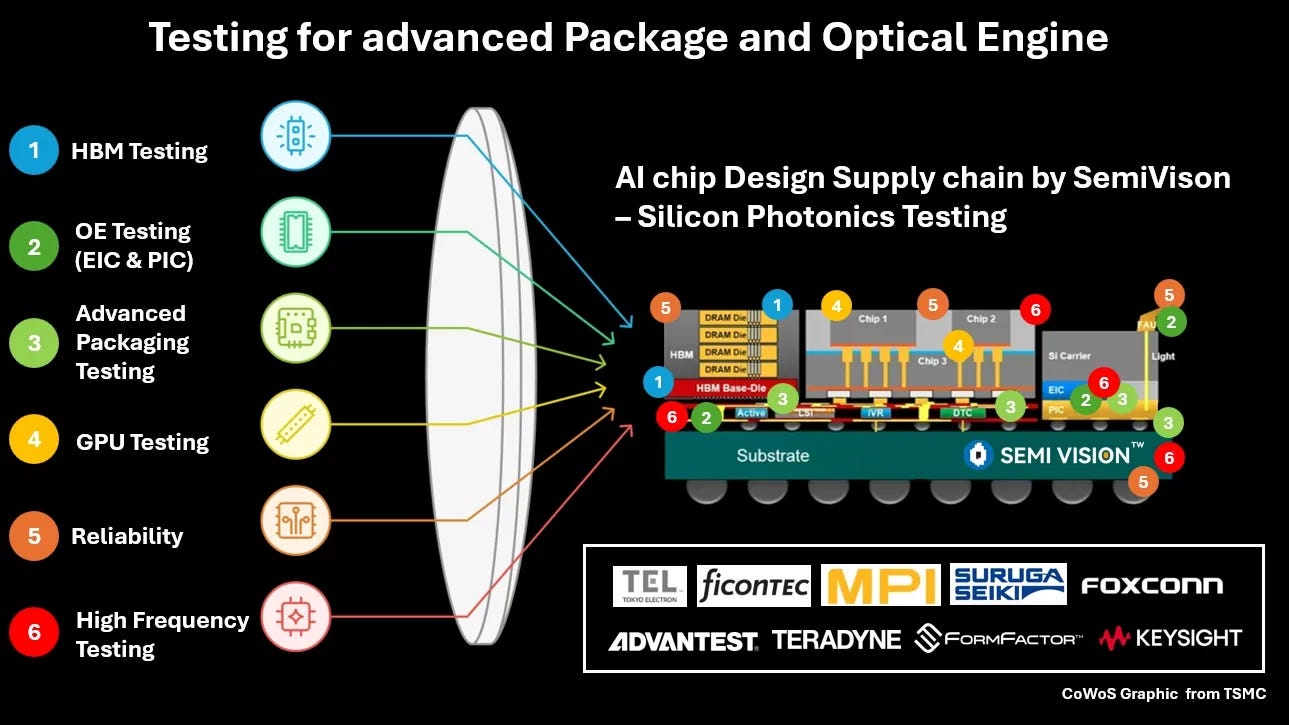
In addition to equipment suppliers, probe card companies such as FormFactor have formed alliances with Advantest, providing high-density probe and test solutions for silicon photonics and 2.5D/3D packaging.
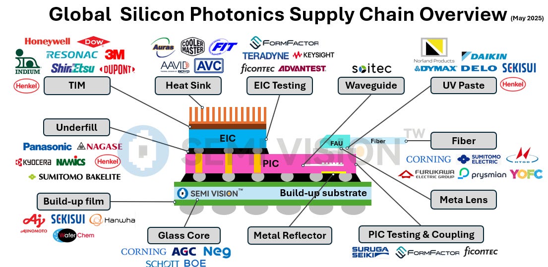
For silicon photonics solutions, we currently see ficonTEC, MPI, and Suruga Seiki offering corresponding systems, with double‑side testing technology as the key focus for all of them.
As AI chips continue to grow in size and power consumption, test times inevitably increase, while reliability remains a non-negotiable priority. To ensure stable performance in real-world applications, the industry widely adoptsburn-in testing, which applies high-temperature and high-voltage accelerated stress conditions to induce early failures in weak components before shipment. This process effectively filters out initial defects corresponding to the early-failure phase of the “bathtub curve,” ensuring the product maintains high reliability throughout its operational lifetime.
For Paid Members , SemiVision will discuss topics on
AI and HPC Driving a New Era in Semiconductor Testing: From ATE to SLT in Technology Evolution and Market Growth
Importance of Burn-In Testing
Reasons for Longer Burn-In Times in AI Chips
Testing’s Background and Industry Overview
Current Development Progress and Public Information
High-Density and Double-Side Testing Solutions for Silicon Photonics: A Comparative Overview of FormFactor, ficonTEC, and MPI
-
FormFactor × Advantest Alliance
-
ficonTEC × Teradyne Dual-Side Testing Solution
-
MPI – Multi-Function Silicon Photonics Probing Systems
Market Trends and Industry Applications
Future Impact and Potential Opportunities
Technical Principles and Testing Challenges
Market Trends and Application Scenarios
The Duel of the Test Giants: Advantest vs. Teradyne in the High-Speed Interface Race
New Opportunities for Taiwanese Manufacturers: The Future Outlook for Probe Cards, Fixtures, and ATE Component Supply Chains
Layered Test Architecture: A Blue Ocean Strategy for AI Packaging Testing from Wafer to Module
Taiwanese ATE Makers Aim for Transformation: From Component Supply to Full System ODM – Who Will Break Through?
Advantest’s Silicon Photonics Strategy: Focused on Photonic Chip and Advanced Packaging Test Platforms
AI and HPC Driving a New Era in Semiconductor Testing: From ATE to SLT in Technology Evolution and Market Growth
With the rapid expansion of AI and HPC applications, the importance of semiconductor testing processes is steadily increasing. Overall, the testing process can be divided into wafer testing (CP, Wafer Probe), final testing (FT, Final Test), and system-level testing (SLT, System Level Test).
CP primarily tests bare dies before packaging by using a probe card to contact the die pads, verifying voltage, current, timing, and functional characteristics. FT is conducted after the chip is packaged, performing full functional and environmental tests to ensure the product operates within design specifications, and sorting the chips by yield using a handler. SLT simulates real-world application scenarios at the board or system level, enabling the simultaneous testing of multiple chips and offering clear advantages in reducing final testing costs for highly complex chips.
Each type of test equipment plays a distinct role in these processes: the ATE (Automated Test Equipment) generates and receives test signals and serves as the core system; probers and probe cards are mainly used in wafer testing to ensure precise electrical contact; handlers are used in final testing to sort chips and can be equipped with Active Thermal Control (ATC) modules for tri-temperature testing (high, ambient, low); and SLT systems are deployed for highly integrated tests that closely replicate actual operating environments, making them particularly suitable for high-power, complex AI and HPC chips.
Advanced packaging brings both significant challenges and strong drivers for test equipment. AI and HPC chips extensively adopt 2.5D/3D packaging and multi-chiplet architectures, relying on high-bandwidth interconnects (such as PCIe and CXL) for high-performance computing. These packaging approaches dramatically increase test complexity, requiring test equipment to support high-speed data links, high-precision alignment, multi-protocol parallel testing, and advanced thermal management.
Meanwhile, large chips such as NVIDIA’s B200, GB200, and RUBIN now have single-device power consumption ranging from 700W to 1800W, necessitating extended stabilization times and strict temperature control during testing. As single-chip sizes grow and transistor counts surge, the number of chips tested per cycle decreases, test times increase, and capacity bottlenecks emerge—driving greater demand for ATE, handlers, and SLT systems. This is the key reason why major manufacturers are actively expanding advanced test platforms and thermal control solutions.
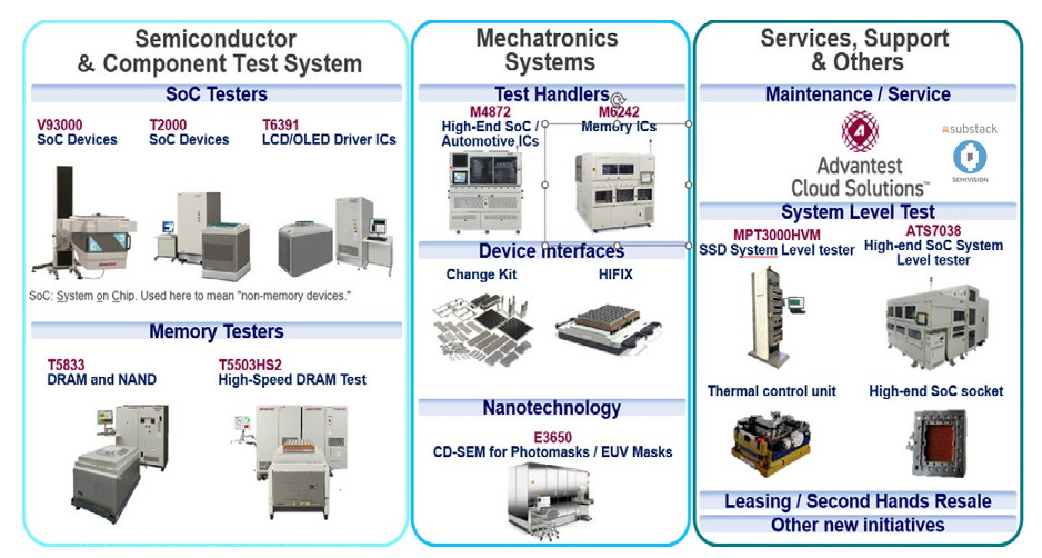
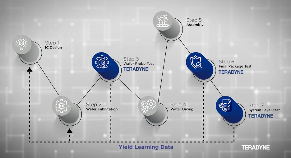

Taiwan’s supply chain also plays a critical role in this space. Hon Precision specializes in handlers and ATC thermal control systems, offering tri-temperature testing capabilities from -70°C to 175°C, and holds about 30% global market share in handlers. Chroma ATE focuses on SLT systems, with its 3210 model certified by U.S.-based AI customers. MPI Corporation is the world’s largest test socket supplier and is investing in probe cards and automated silicon photonics testing systems. CHPT is working with Cohu to develop millimeter-wave probe cards supporting frequencies above 60 GHz. MPI’s rival, WinWay Technology, specializes in vertical probe cards and high-speed test sockets, and also offers thermal management solutions for CPO packaging. Together, these global and Taiwanese companies form a complete ecosystem spanning ATE cores, probe cards, handlers, and SLT integration.
Importance of Burn-In Testing
Burn-in testing is a form ofAccelerated Reliability Testingthat applies high-voltage and high-temperature stress to trigger potential defects and early failures within a short period. For AI chips, the high integration of logic and memory modules (such as HBM) means that inherent defects can cause system-level crashes, making burn-in the most effective method for screening early failures.
HTOL (High Temperature Operating Life) is an extended form of burn-in testing, where devices operate under elevated temperatures and load conditions (e.g., above 125 °C for several hundred hours) to estimate lifespan and evaluate failure mechanisms. AI chips typically combine both static and dynamic stimuli, inducing large amounts of toggle activity within the chip to accelerate aging.
Reasons for Longer Burn-In Times in AI Chips
Increased chip complexity:For example, NVIDIA’s Blackwell series GPUs reportedly require burn-in times 3 to 4 times longer than the previous Hopper generation. This growth reflects the need to proportionally extend burn-in duration.
Test duration increase from 600–800 seconds to 1200–1600 seconds:Initial empirical plans may allocate 600–800 seconds for burn-in under high power, high heat, and multi-module operation, but as testing experience grows and quality standards tighten, the actual requirement has risen to 1200–1600 seconds or more to meet reliability targets and lifetime projections.
Higher sensitivity to failure rates:If early failures are not screened out, they can cause large-scale operational disruptions in data centers, further driving longer and more comprehensive burn-in coverage.
Evolution from Wafer-Level to Package-Level Burn-In
In recent years, the industry has explored shifting burn-in testing from the package level to the wafer level to improve efficiency and reduce costs. This “shift-left” strategy can leverage machine learning anomaly detection during accelerated life testing to screen out potential defects earlier. However, because AI chips often use multi-die stacking with dense micro-bump interconnects, post-package interconnect integrity still needs verification. Therefore, package-level burn-in remains indispensable, particularly for ensuring final product quality.
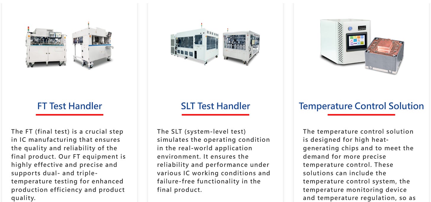
Hon Precision Product

Looking ahead, sales of semiconductor test equipment are projected to grow by 15.1% in 2025 and 20.6% in 2026, driven primarily by AI/HPC packaging demand and the adoption of advanced process nodes. In particular, TSMC’s CoWoS capacity is expected to expand from 70,000 wafers per month in 2025 to 150,000 wafers per month in 2027, directly boosting demand for high-end test equipment. SLT offers clear cost advantages in an era of increasingly complex chips, complementing rather than replacing FT. Overall, AI and advanced packaging are propelling semiconductor test equipment into a new growth cycle, with both technical barriers and capacity requirements rising in tandem—making test equipment an indispensable element for ensuring chip performance and yield.
The global semiconductor testing market is experiencing sustained rapid growth under strong demand from AI and high-performance computing (HPC). Leading test vendor Teradyne has significantly raised its market outlook, reflecting the direct impact of surging AI chip demand. According to the latest data, Teradyne has revised its 2024 market size forecasts for SoC and memory testers to $4.2 billion and $5.6 billion, respectively—up from the previous $4.6 billion and $1.7–1.9 billion—and expects further growth to $4.9 billion for SoC testers and $1.4 billion for memory testers in 2025.
Breaking down by application segment, compute-related SoC test demand is the strongest, with the 2024 market size revised upward from $2.2 billion to $2.3 billion, underscoring AI compute chips as the primary driver of the overall testing market.

The rise in testing demand is closely linked to chip design evolution. Increases in die size and transistor counts have created significant challenges for testing. For example, NVIDIA’s GPU lineup—from H100 and H200 to B200 and the latest RUBIN architecture—shows a steady growth in die size, reducing the number of bare dies per wafer. While traditional consumer products can be tested 16 units at a time in a handler, high-end ASICs and GPUs, due to their large die size, often allow only 2–3 units per test cycle. Meanwhile, transistor counts and power consumption have surged, with the B200 reaching 1,000 W, GB200 at 1,200 W, and RUBIN up to 1,800 W. High power levels impose heavy cooling and power delivery demands and extend stabilization times during testing, doubling or tripling total test durations compared to conventional devices.
As die sizes grow and chips become more power-hungry and complex, the number of devices tested per cycle falls, individual test times lengthen, and production test capacity comes under strain—directly increasing demand for more ATE, handlers, and SLT systems.
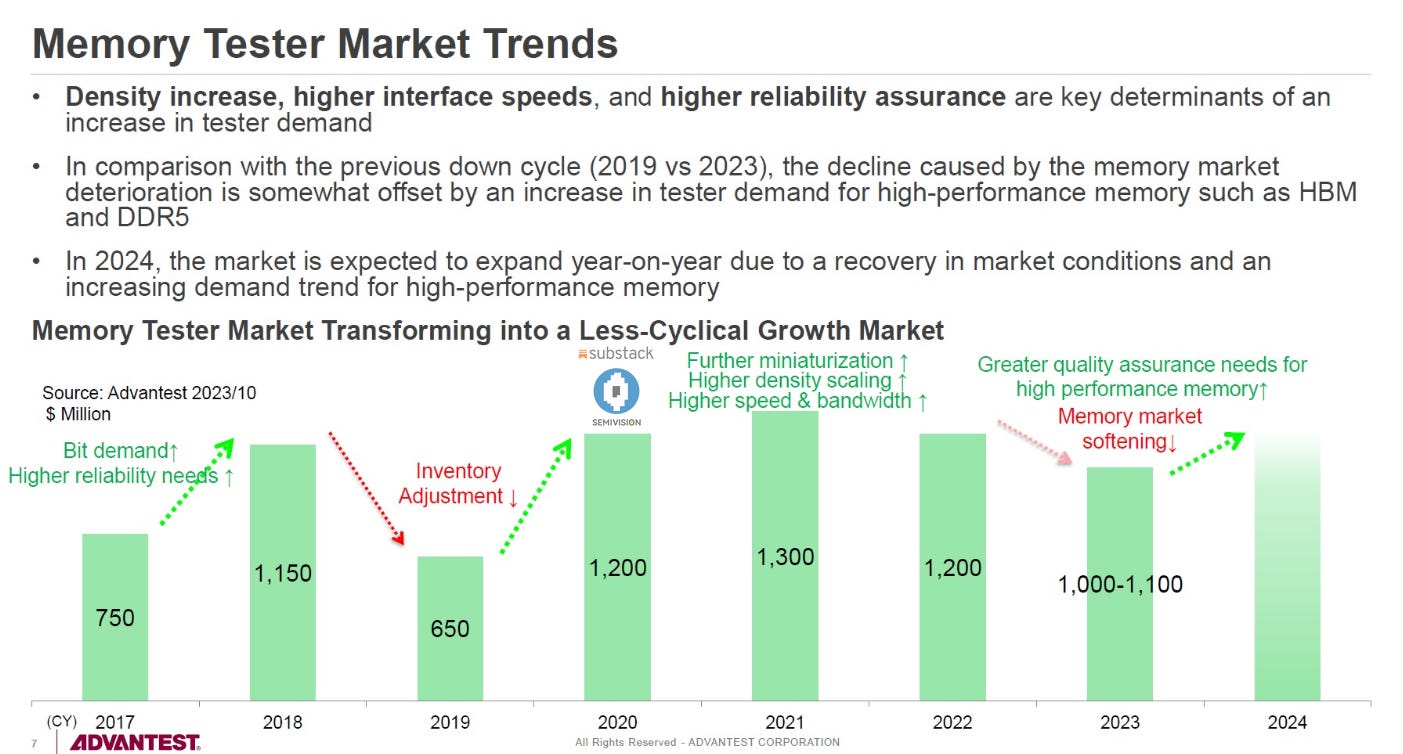
From a market structure perspective, SoC testers dominate with 77% share, while memory testers account for around 23%. SoC testing can be further divided into compute, mobile, industrial/auto, and SoC service segments, with compute holding the largest share. Thanks to robust demand for AI compute chips—including GPUs and various ASICs—this segment is the main growth driver. Market research projects the SoC test market to grow at an 8.01% CAGR from 2025 to 2030, while the memory test market will see a 7.63% CAGR, both benefiting from AI’s sustained demand for high-bandwidth memory (HBM) and accelerators. Segment-level data further shows compute’s share of the SoC test market rising from 35% in 2023 to 46.9% in 2025, while mobile, industrial/auto, and SoC services remain relatively stable—indicating that high-compute-demand products will remain the core growth engine.
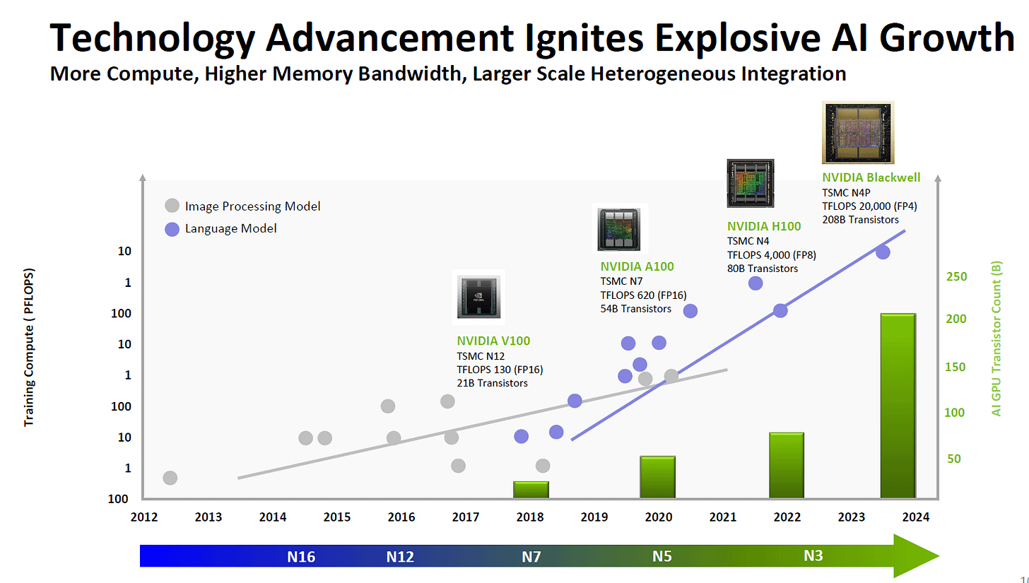
In summary, the generational evolution of AI and HPC chips is reshaping the semiconductor test market’s structure and demand patterns. Larger die sizes, skyrocketing transistor counts, and kilowatt-class power levels have extended test times, reduced per-cycle test throughput, and stressed production capacity—forcing semiconductor manufacturers and test equipment vendors to deploy more ATE and advanced handler systems, and to develop multi-temperature, multi-protocol, high-precision test platforms. In this environment, SLT is gaining importance, as it allows multiple chips to be tested under realistic operating conditions, reducing overall test costs and improving efficiency. Over the next several years, as foundries like TSMC expand CoWoS and chiplet packaging capacity, the test equipment market is expected to sustain high growth—evolving toward a SoC-centric, compute-driven profile under the momentum of the AI compute race.
Testing’s Background and Industry Overview
Advantest is a leading Japanese supplier of semiconductor test equipment, specializing in automated test equipment (ATE) for wafer-level testing as well as electronic measurement instruments. In the global semiconductor test equipment market, Advantest and U.S.-based Teradyne dominate, with a combined market share of around 80%. In 2023, Advantest held roughly 50% market share, while Teradyne held about 30%. Industry commentators often compare Advantest’s market dominance to ASML’s position in lithography, earning it the nickname “the ASML of semiconductor testing.”
Technical Fundamentals and Testing Challenges
Driven by AI and high-performance computing (HPC) demand, semiconductor chips are increasingly moving toward advanced packaging and multi-chip integration, which significantly raises the complexity of testing. Modern AI chips often adopt 2.5D/3D packaging, such as integrating CPUs or SoCs with HBM (High Bandwidth Memory) stacks, or utilizing high-speed optical interconnects like CXL and PCIe for chip-to-chip communication.
These packaging approaches requirecomplex wafer-level and final package testing, demanding test equipment with:
Extremely high communication bandwidth
Precise alignment capabilities
Multi-protocol parallel test support
For example, Advantest’s MPT3000 SSD test platform has achieved PCIe 5.0 compliance certification, supporting NVMe devices and components using Compute Express Link (CXL). To address high‑power thermal challenges, it incorporates dedicated thermal interface panels and engineering thermal chambers to manage temperatures during high-speed SSD testing.
Overall, AI chip testing faces challenges in multi-protocol validation, high‑bandwidth signal integrity, temperature management, and sample stability, requiring advanced probe cards, test fixtures, and high-speed data transmission architectures.
Current Development Progress and Public Information
The semiconductor test equipment market is currently dominated by a few key players, including Advantest, Teradyne, FormFactor, MPI (also known as MPI Corporation), and ficonTEC. Each company is actively advancing its product lines to address AI, HPC, and advanced packaging testing requirements:
- Advantest (Japan)
Continues tolaunch next-generation test platforms:
MPT3000 SSD Test System– PCIe 5.0 compliant, supportsNVMe and CXL component testing.
V93000 SoC Series– Equipped withXtremeLinktechnology, enablingultra‑high‑speed data linksfor SoC and logic device testing.
Focus:High-bandwidth, multi‑protocol, and thermally managed testingfor AI and advanced packaging devices.
- Teradyne (United States)
OffersUltraFLEXandJ750 seriestest systems, supportinghigh-volume SoC and logic testing.
Actively developingAI‑oriented solutionsand integrating system‑level test (SLT) capabilities to meet thegrowing AI chip demand.
- FormFactor (United States)
Recently unveiled theTRITON Test SystematOFC 2025, co‑developed withAdvantest and Tokyo Electron (TEL):
Designed for silicon photonics (SiPh) wafer-level testing and CPO (Co-Packaged Optics).
Combines optical and electrical testing, allowing simultaneous light‑path and circuit validation toaccelerate AI component production ramp‑up.
Leverages itshigh-density probe card expertiseto support advanced optical and 2.5D/3D packaging test.
- MPI Corporation (Taiwan)
Focuses onprobe cards and test sockets, and is activelyexpanding into SiPh automated test solutions.
According to its latest annual report:
World’s largest test socket supplier.
Provideshigh‑pin‑count and high‑temperature probe cardsfor 2.5D/3D and AI chip testing.
Future direction:Integrating generative AIinto automated test software toaccelerate new application development.
- Other Probe Card and Interface Technology Suppliers
Chunghwa Precision Test (CPT)– Collaborates withCohuto developmmWave probe card solutions, supporting frequencies above60 GHz.
WinWay Technology– Specializes invertical probe cards and high‑speed sockets, including:
Vertical docking probe cardsforCPO packaging.
Integrated thermal management solutionsfor high‑power optical and AI devices.
These companies leverage their respective strengths—from ATE platforms and system‑level testing to probe card and optical interface technologies—and often partner with global test equipment leaders. Their collective focus is to enhance AI, SiPh, and advanced packaging test capabilities, supporting the next wave of HPC and AI semiconductor production.

High-Density and Double-Side Testing Solutions for Silicon Photonics: A Comparative Overview of FormFactor, ficonTEC, and MPI
In silicon photonics and advanced packaging—particularly in 2.5D/3D integration—testing complexity has increased sharply, driving demand for high-density and double-side wafer-level testing capabilities. Below is an in-depth review and comparison of three leading probe card and test system providers—FormFactor,ficonTEC, andMPI—focusing on their silicon photonics measurement solutions.
- FormFactor × Advantest Alliance
Partnership Background
Since 2024, FormFactor and Advantest have collaborated on wafer-level testing solutions for silicon photonic chips. In 2025, the partnership deepened through expanded technical and equity cooperation, establishing a strategic alliance.
Key Technical Highlights
9-Axis Nanometer-Precision Alignment System– Among the fastest fully automated optical alignment modules worldwide.
Fully Integrated Test Environment– Combines FormFactor’sVelox™probe station control andOptoVue™ Prowith Advantest’s V93000 ATE platform, seamlessly linked through theSmarTest 8software to support optoelectronic co-testing and thermal test sequences.
Apollo Architecture + Pharos™ Optical Probe Technology– Enables ultra-low coupling loss with high-volume compatibility and minimal drift during packaging processes.
Applications
Supports wafer-level surface and edge coupling tests, with compatibility forco-packaged optics (CPO)and advanced packaging process flows.
- ficonTEC × Teradyne Dual-Side Testing Solution
Partnership
ficonTEC and Teradyne jointly launched the industry’s firsthigh-throughput, double-sided electro-optical wafer test system.
Product Features
300 mm Dual-Side Test Platform– Electrical testing (DC / high-speed) is performed on the top side, while the bottom side conducts optical alignment and optical I/O measurements.
Direct Integration with UltraFLEXplus ATE (IG-XL)– Includes wafer handling, automated calibration, and vacuum thermal control chuck capabilities.
In-Situ Fiber Array Calibration + Six-Axis Optical Alignment– Ensures stable and reliable electro-optical coupling measurements, ideal for CPO and PIC/EIC integrated devices.
ficonTEC Introduces Industry’s First, ATE Agnostic, Top-Sided Electro-optical Wafer-level Tester
Applications
Designed for high-end silicon photonics and packaging lines requiring simultaneous dual-side coupling tests in production environments.
- MPI – Multi-Function Silicon Photonics Probing Systems
Product Portfolio
MPI offers upgradable SiPH probe modules (TS2000-IFE/TS3000-SiPH), purpose-built for silicon photonics wafer-level testing.
Core Technologies
Precision Fiber Alignment– Supports ultra-fast scanning, multi-fiber arrays, and Z-sensing contact detection.
Flexible Test Modes– Capable of optical-to-optical (O-O), optical-to-electrical (O-E), electrical-to-optical (E-O), and electrical-to-electrical (E-E) measurements.
Broad Environmental Support– Operates from –50°C to 200°C, with optional dark-box environments to eliminate optical interference.
Sentio® Multi-Touch Control Platform– Intuitive interface, compatible with mainstream probe stations, and supports rapid test integration via sample scripts.
Applications
Best suited forR&D and engineering validation phases, while also supporting medium-volume production with high configurability.
FormFactor × Advantesttargetshigh-volume manufacturingwith integrated ATE compatibility and nanometer-level optical alignment.
ficonTEC × Teradynepioneersdual-side testingfor production-scale CPO and PIC/EIC devices.
MPIoffersversatile, modular systemsideal for R&D and engineering, with flexibility to adapt to diverse optical and electrical test needs.
As silicon photonics continues to advance—particularly in AI/HPC, co-packaged optics, and heterogeneous integration—these testing solutions are becoming critical to ensuring device performance, yield, and scalability.
Market Trends and Industry Applications
The global semiconductor test equipment market is experiencing rapid growth under the AI boom. According to market research, the market size surged by approximately 36% in 2024, reaching a record high of USD 6 billion, primarily driven by demand for high-performance computing (HPC) chips and high-speed memory. Both memory testing (including HBM) and SoC testing expanded significantly.
Advantest’s 2024 revenue doubled, with logic test sales up 70% and memory test sales more than tripling. On the application side, AI data center servers, 5G communication infrastructure, and future autonomous driving ADAS chips have triggered a sharp rise in testing demand for 3D packaging and silicon photonic interconnect devices. For example, as AI servers such as NVIDIA’s H100 and GB200 enter mass production, testing needs for silicon photonics optical engines and HBM devices have also increased in parallel.
Additionally, automotive electronics and IoT devices are increasingly adopting AI computing modules, driving growth in final test (FT) and system-level test (SLT) markets. These factors together shape a market trend that places extremely high demands on advanced test equipment, underscoring the importance ofhigh-efficiency, high-accuracy, and versatiletesting solutions.

Future Impact and Potential Opportunities
Looking ahead, AI and advanced packaging will remain the primary drivers of semiconductor testing. While industry leaders such as Advantest and Teradyne already dominate the market, they can maintain their lead through continuous innovation. Sub-5nm advanced process nodes and more complex multi-layer 3D packaging will continue to increase the test content per chip, further driving demand for high-performance test platforms.
For Taiwan’s test industry, surging AI demand means higher wafer volumes and increased need for customized solutions, creating opportunities for local players to move up from component manufacturing to full system integration. On the other hand, a high 2024 baseline and currency fluctuations are expected to slow growth momentum in 2025: Advantest has already revised its 2025 revenue forecast down by 3.2% due to the elevated 2024 base and a strong USD/JPY exchange rate. Excluding currency effects, however, the market is still expected to expand by about 10% for the second consecutive year.
In the near term, operational pressure will persist, but long-term opportunities remain. Potential growth drivers include:
Test houses increasing investments in advanced test equipment.
Test service providers vertically integrating to develop in-house test platforms, improving margins.
Companies that can capture the core needs of AI-era testing and invest early in emerging areas such as silicon photonics and co-packaged optics (CPO) will have the chance to expand their influence in the global test market.
The Testing Revolution in the AI Era: How HBM Testing Propelled Advantest’s Growth
Background and Industry Overview
High Bandwidth Memory (HBM) is a type of 3D-stacked DRAM with extremely high data transfer rates, often tightly integrated with GPUs or AI accelerators. As AI inference and training workloads surge, HBM plays a critical role in AI data center servers, often becoming the system performance bottleneck. At the same time, HBM’s complex packaging and fine-pitch interconnects impose stringent testing requirements.
Advantest has responded to this trend by strengthening its memory test product line, particularly for HBM and next-generation packaging test solutions. Recent market research shows that HBM-related testing now accounts for roughly 50% of Advantest’s memory test revenue—clear evidence of HBM testing’s contribution to growth.
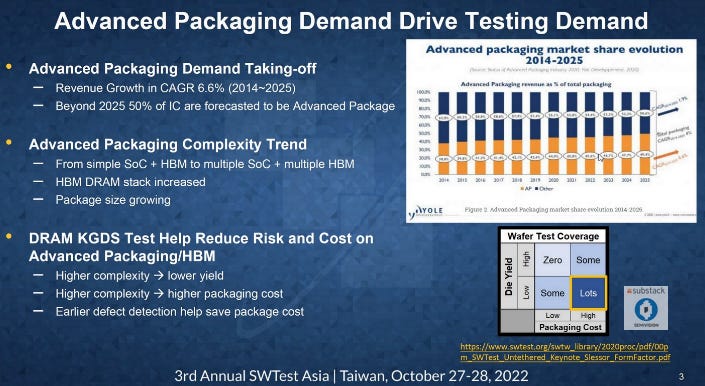
Technical Principles and Testing Challenges
HBM devices typically consist of multiple DRAM dies stacked vertically (e.g., via 3D TSV technology) to form a large-capacity module, connected to processors via high-speed interfaces. Testing is required both before and after stacking, covering functional verification of each die and system-level testing after final packaging.

The complex stack structure means each die layer and interface can produce failure modes, significantly increasing the number of test vectors and total test time. High-end testers from companies like Advantest must therefore support high multi-site and high parallelism capabilities, as well as dedicated HBM protocols and high-speed, high-frequency test functions (e.g., high-speed command/return channels, high-frequency clocking).
For example, Advantest’s MPT3000 SSD test platform can test NVMe SSDs driven by HBM and is PCIe 5.0-certified, demonstrating its capability to handle extremely high-bandwidth test workloads. Power consumption and thermal management are also critical—test systems must integrate active thermal control to maintain chip stability during testing, ensuring consistent and reliable results.
Current Developments and Public Information
In the HBM and high-end memory test segment, Advantest and other equipment vendors are accelerating their technology deployments. According to Reuters, Advantest confirmed that HBM testing accounts for about half of its memory test revenue, with demand surging due to AI computing requirements—prompting the company to raise its 2024 memory test sales forecast.
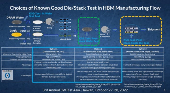
Advantest’s memory test systems, such as the FIVR series, already support multiple advanced memory standards including HBM. At the same time, major global memory manufacturers such as Samsung and SK hynix are rapidly expanding HBM production capacity, ensuring stable growth in test demand. Competitors like Teradyne are also developing high-frequency memory test solutions, often in partnership with probe card suppliers like FormFactor to deliver complete HBM test offerings. Taiwan-based MPI, one of the world’s largest test socket providers, is investing in vertical probe card and MEMS probe technologies for stacked-die applications such as HBM.
Market Trends and Application Scenarios
AI accelerators—GPUs, ASICs, FPGAs—are frequently integrated with HBM to meet HPC requirements. As the AI cloud services and HPC markets expand, HBM chip and module shipments are increasing sharply, driving demand for HBM test equipment.
According to Advantest, the memory test market grew significantly in 2024, with high-performance memory such as HBM and HBM2e more than doubling in market size compared with the previous year. This suggests continued benefits for test equipment vendors.
On the application side, HBM is widely used in AI training cards, data center servers, and HPC platforms. It also appears in autonomous driving AI compute units, high-frequency trading systems, and other domains—each requiring comprehensive and reliable testing processes. As a result, test solutions extend beyond wafer fabs to OSAT providers and even large cloud service operators that run in-house test centers, creating a complete supply chain demand.
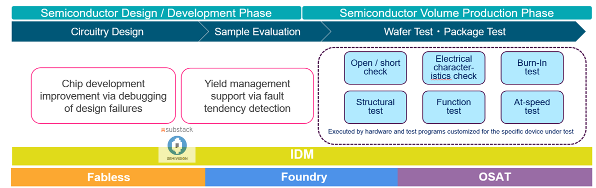
Future Outlook and Opportunities
In the AI era, HBM testing is a powerful growth engine for Advantest. Statements such as “HBM accounts for nearly 50% of our memory test business” reflect how the integration of HBM into more AI chips is amplifying demand for advanced testing.

However, competition is intensifying. If emerging domestic or Chinese test vendors accelerate the development of self-designed test platforms, they could challenge traditional leaders. Advantest and others will therefore need to sustain technological innovation while maintaining leadership in capacity and customer support to continue benefiting from the HBM-driven market expansion.


The Duel of the Test Giants: Advantest vs. Teradyne in the High-Speed Interface Race
Background and Industry Overview
Advantest (Japan) and Teradyne (U.S.) are the two dominant players in the global Automated Test Equipment (ATE) market, together holding roughly 80% market share. Both companies have strong technology portfolios and customer bases, competing head-to-head in the high-end testing segment.
As semiconductor technology advances, high-speed interfaces—such as PCIe, CXL, USB, and ultra-high-speed memory links—have become critical in chip design and a new battleground for test platforms. Both companies are actively working to support next-generation high-speed protocols and packaging formats, aiming to secure high-margin business in the premium segment.
Technical Fundamentals and Testing Challenges
High-speed interface testing includes high-frequency digital signal integrity checks, protocol compliance testing, and related interconnect verification.
For example, PCIe 5.0 and CXL require test systems to generate and analyze signals at tens of gigabits per second with high accuracy, as well as conduct long-duration stress tests. This demands testers that combine high-speed digital I/O, precise timing control, and dedicated protocol handling capabilities.
Advantest’s MPT3000 SSD test platform has achieved PCIe 5.0 compliance certification, proving its ability to perform production-line compliance testing for NVMe and CXL devices.

In another direction, high-speed SoC internal IP testing is often realized via advanced packaging interconnects. For multi-chip module-based SoCs, testers must simultaneously validate both electrical (logic) and optical interconnects (e.g., silicon photonics or fiber optics). This requires multi-protocol, multi-channel parallel testing and the ability to combine electrical and optical measurements on the same platform—such as withFormFactor’s TRITON system.
The test process also frequently employs thermal chambers, signal conditioners, and dynamic equalization techniques to suppress noise and jitter during high-speed transmission, ensuring accurate results.
Current Developments and Public Information
In high-speed interface testing, both Advantest and Teradyne are accelerating platform launches and partnerships.
Advantest
Expanded the MPT3000 series to support PCIe 5.0 and CXL compliance testing.
Introduced new thermal control accessories to address thermal mismatch issues.
Added high-speed scan andXtremeLinkfeatures to its V93000 SoC test platform for embedded high-speed interface testing.
Collaborating with probe card vendors to develop higher-bandwidth probing solutions.
Teradyne
Continues upgrading its flagship UltraFLEXplus SoC test platform with higher bandwidth and modular test resources, supporting various high-speed serial links.
Partnered with global communication test instrument suppliers to integrate analysis equipment for improved measurement accuracy.
Both companies are also investing insystem-level test (SLT) capabilities—beyond wafer-level test—adding Ethernet and optical communication interface testing to serve 5G base station and data center networking chips.
Market Trends and Application Scenarios
The global demand for high-speed interface testing is driven by the need for fast data transfer across multiple sectors:
Data Centers: AI accelerators like NVIDIA Hopper/Grace with HBM and CXL architectures require reliable data transfer at 10 GB/s or higher. Test systems must simulate massive data loads and verify timing accuracy.
Consumer Electronics & 5G: Mobile and communication SoCs integrate PCIe 4.0/5.0, high-speed USB, and similar interfaces—requiring compliance coverage at both wafer and package test stages.
Automotive Electronics: Domain controllers and advanced sensors are increasingly using high-speed communication links, expanding the testing market.
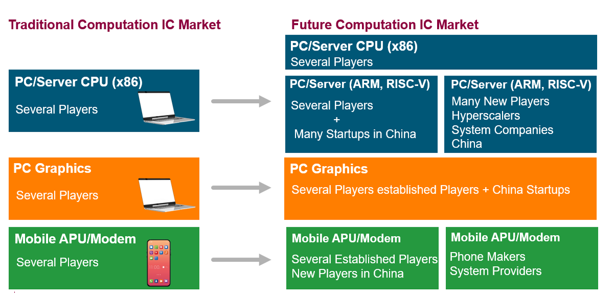
Overall, protocol compliance testing and the associated horizontal test equipment demand are growing rapidly, highlighting the industry’s clear shift towardmulti-protocol, high-speedcapabilities. Analysts point out that AI servers and 5G infrastructure have become new growth engines for test equipment, providing strong revenue support to both Advantest and Teradyne in 2024–2025.
Future Impact and Opportunities
The challenges and requirements of high-speed interface testing will continue to generate business opportunities for both giants:
Next-Gen Protocol Readiness– With PCIe 6.0, CXL 2.0, and future data rates moving from today’s 10 Tbit/s toward several dozen Tbit/s, test platforms must keep pace with frequent spec updates. Advantest and Teradyne can leverage their technical leadership to launch next-generation high-speed test solutions and reinforce market share.
Optical Testing Integration– Both may deepen collaboration with optical test technology providers to meet silicon photonics and co-packaged optics (CPO) requirements. FormFactor’s TRITON system already integrates electrical/optical test; Teradyne could gain an edge by adopting similar capabilities.
Taiwan Industry Opportunities– Rising demand for related test components—such as probe cards and load boards—offers opportunities for Taiwanese suppliers to grow by serving both major ATE makers.

However, breaking through product standardization and high technical barriers remains challenging. Only companies that continue innovating and building strategic alliances—such as Advantest partnering with FormFactor/TEL for integrated solutions—are likely to secure an advantage in the ongoing high-speed interface testing race.

New Opportunities for Taiwanese Manufacturers: The Future Outlook for Probe Cards, Fixtures, and ATE Component Supply Chains
Background and Industry Overview
Taiwan has long played a critical role in the global semiconductor testing supply chain as a key supplier of high-value components. With the global test equipment market dominated by a handful of foreign companies, Taiwanese manufacturers have primarily focused on the development and production of essential parts such as probe cards, test sockets, and test fixtures.
Companies like CHPT, Winway Technology, and MPI Corporation provide high-end probe cards and test interface boards for wafer-level and package-level testing. These components form the crucial link between the device under test (DUT) and the automated test equipment (ATE), making them indispensable in test systems. As the AI era drives a surge in packaging and testing demand, Taiwanese suppliers face unprecedented opportunities in the components market.
Technical Fundamentals and Testing Challenges
Aprobe cardis used for wafer-level testing, requiring precise contact with chip pads or bumps. High-frequency probe cards must also support optical coupling and RF signal transmission. Manufacturing high-pin-count probe cards for micro-bump alignment demands advanced MEMS probe fabrication and ultra-precise positioning technologies.
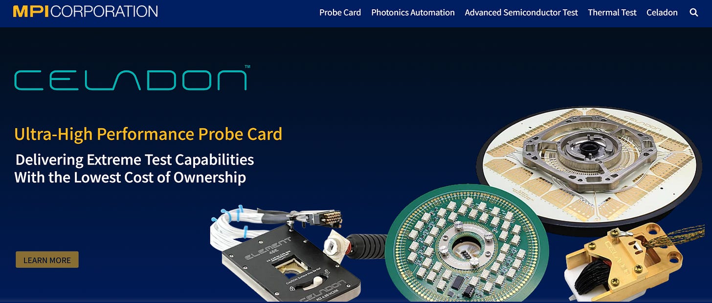
At the module or system level,test fixturesandtest socketsare critical for securely mounting and connecting complex packaging formats—such as Package-on-Package (PoP), System-in-Package (SiP), and 2.5D/3D ICs—to the test system, while meeting stringent requirements for high-power thermal dissipation and high-speed signal integrity.
With the rise ofsilicon photonicsandco-packaged optics (CPO)testing, certain next-generation probe cards must integrate optical fiber alignment capabilities and provide consistent testing solutions across multiple stages—wafer probe, burn-in, and final test. The key technical challenge is to achieve high-speed performance, repeatable alignment, and mass production capability, while balancing cost and precision.
Market Trends and Industry Applications
With the surge in demand for AI chips and advanced packaging, the need for testing components is expanding in parallel. High-pin-count probe cards and high-efficiency thermal test sockets have become standard in areas such as silicon photonics and 3D packaging, where specifications and quality requirements are extremely stringent. In practical applications, AI computing chip testing, automotive chip testing, and 5G RF chip testing all rely on highly reliable probe cards and test interfaces.
For example, in module testing, the device under test must be securely mounted in the test socket while maintaining signal integrity; in high-temperature burn-in testing, test fixtures must withstand prolonged thermal cycling. These requirements are driving probe card and fixture suppliers to offer customized, integrated solutions. From a market perspective, both domestic and export opportunities coexist: international wafer fabs and OSATs depend on precision components from Taiwanese suppliers, while domestic testing service providers may also absorb local demand by extending production lines to self-made test equipment. Some analysts note that, as AI demand grows, certain wafer testing houses may even develop their own test systems to reduce outsourcing costs and improve margins—indirectly boosting demand for high-end probe cards and fixtures.
Future Impact and Potential Opportunities
Looking ahead, the probe card and test fixture market will continue to benefit from the momentum of advanced processes and 3D packaging. Companies such as CHPT and Winway could significantly strengthen their global competitiveness if they successfully expand into silicon photonics and CPO-related testing equipment. For instance, ficonTEC has launched a 300 mm double-sided silicon photonics wafer testing system compatible with existing ATE architectures—a breakthrough that offers new design references for probe card manufacturers.
Potential opportunities include developing higher-bandwidth probe cards, integrated test interfaces (combining electrical and optical testing), and customized solutions for specialized applications such as automotive and aerospace. If Taiwanese suppliers can master automated production and smart manufacturing practices, while aligning with international standards (e.g., through partnerships with companies like Cohu), they will be well-positioned for transformation and upgrading.
Furthermore, the probe card and fixture sector may foster third-party testing services or OEM opportunities: local vendors could integrate components into turnkey test systems, undertake complete system contract manufacturing, or help global majors accelerate time-to-market. In short, Taiwan’s accumulated technical expertise and supply chain strengths in testing components will continue to hold value in the AI era. With sustained innovation and an expanded technology scope, they have a strong chance to “break through” in the global testing market.
Background and Current Industry Landscape
As 2025 begins, Advantest faces multiple variables that could affect its performance. In 2024, the company benefited from a boom in AI semiconductor testing demand, driving revenue growth of over 60%. However, with this high base, its 2025 outlook is more cautious. The company has projected a revenue decline of about 3.2% for the fiscal year, mainly due to the high base effect and the Japanese yen’s historically low exchange rate against the U.S. dollar—which had been a tailwind for exporters but has recently lost momentum. In addition, geopolitical risks and global economic uncertainty remain key challenges. Nevertheless, demand in its core markets remains strong—AI servers and high-performance computing (HPC) continue to drive SoC and memory testing needs, providing ongoing momentum.
Technical Fundamentals and Testing Challenges
In the advanced testing domains where Advantest excels, new packaging and process technologies bring both challenges and opportunities. Increasing complexity in semiconductor packaging—such as 3D ICs and system-in-package—means more test points and more complex test flows, requiring higher-density, multifunction test systems. As process nodes advance (5nm, 3nm, and beyond), chip architectures become larger (multi-core, highly integrated SoCs), extending scan test and verification cycles.
For Advantest, products must continuously evolve to support more pins, more power domains, and AI-specific test items. Another challenge lies in balancing global deployment of test systems with maintaining technology leadership—especially as China moves toward self-developing ATE systems.
Company Developments and Public Disclosures
Advantest’s 2024 first-half results were exceptional, with memory testing particularly strong. Industry sources attribute part of this to surging HBM testing demand, which has increased the share of memory testing in total revenue. On the product side, Advantest continues to invest in R&D, rolling out new platforms such as an expanded MPT3000 series (supporting more protocols) and an enhanced V93000 to capture emerging market needs.
Meanwhile, competition is intensifying—Teradyne is actively developing advanced SoC test solutions, and OSAT players like KYEC and Sigurd may leverage in-house expertise to develop their own testers, reducing reliance on external suppliers. This trend poses both risks and partnership opportunities. In its November 2024 financial report, Advantest projected that—excluding currency impacts—2025 sales could remain flat or grow, with core market size expanding by roughly 10% and gross margins holding around 58%.
Market Trends and Application Scenarios
In 2025, global semiconductor testing demand is still expected to be driven by AI and HPC, even as automotive and industrial electronics recover more slowly. Advantest’s key customers—including Google, Amazon, and NVIDIA—are expected to keep placing orders for GPU and ASIC testing. Advanced packaging tests, such as 3D wafer testing and full system-level tests, are becoming mainstream, and Advantest has emphasized its investment in these solutions at industry events like Semicon Taiwan.
Currency fluctuations in the Japanese yen and New Taiwan dollar will have ripple effects for both Taiwanese OSATs and Advantest. A stronger yen would be a headwind for Advantest’s exports. Another market factor is the ongoing U.S.–China tech rivalry, which is driving China to pursue self-sufficiency in test equipment. While China still relies on imported high-end testers for advanced processes in the short term, this could become a disruptive factor in the future. Overall, demand for advanced test systems and solutions will remain intact, and as long as Advantest maintains its technology edge and customer stickiness, it can continue to benefit from these trends.
Future Impact and Potential Opportunities
Despite the challenges of 2025, Advantest holds several promising opportunities. First, AI-driven testing demand is set for structural, long-term growth—especially as open AI models and edge computing proliferate, creating more low-latency, high-performance systems requiring full-spectrum testing from wafer to system level.
Second, Advantest can continue optimizing its high-margin business by using customized probe cards and fixtures to improve test efficiency, and by developing software and cloud-based data analytics services to enhance product value. Currency-related gains and losses can be managed via hedging strategies and diversified manufacturing locations, while current yen weakness could be leveraged to boost R&D investment.
Finally, if the company can lead in emerging domains such as AI SoC packaging tests and silicon photonics testing, it could open new “blue ocean” markets in the next few years. In summary, short-term headwinds will mainly come from macro factors such as the high base effect and currency shifts, but over the long run, Advantest’s strong technical capabilities and market position put it in a favorable place to seize future growth opportunities—provided it remains proactive in adapting to market changes.
Layered Test Architecture: A Blue Ocean Strategy for AI Packaging Testing from Wafer to Module
Background and Current Industry Landscape
Semiconductor test architectures have evolved alongside packaging technologies into a layered structure: wafer-level testing (Wafer Test), post-packaging testing (Package/Final Test), and system or module-level testing (System/Module Test). Together, they form a complete test flow.
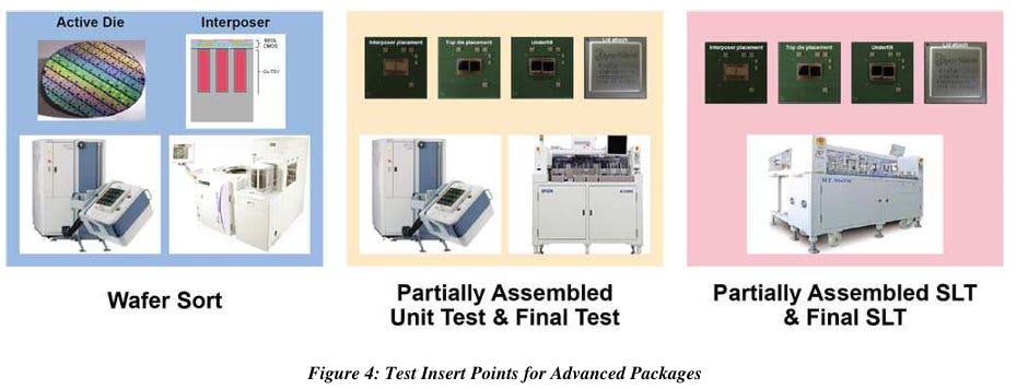
With the integration of AI chips and advanced packaging—such as 2.5D/3D packaging, wafer-level chip-scale packaging (WLCSP), and system-in-package (SiP)—the demand for post-packaging testing is emerging as a “blue ocean” opportunity. The industry increasingly recognizes that wafer testing alone can no longer meet future requirements, and that greater investment in multi-level interface testing will be essential.
Technical Fundamentals and Testing Challenges
The core of the layered testing architecture lies in the fact that each packaging stage has distinct test objectives and challenges:
Wafer Testfocuses on functional screening of individual dies on bare wafers.
Package Testchecks bonding integrity and functional preservation after packaging.
Module/System Testverifies the overall performance and reliability of the final assembled system.
AI packaging modules often integrate multiple chips (e.g., CoWoS) and communication interfaces (e.g., optical interconnects, HBM), which greatly increases the volume and complexity of test requirements. For example, a co-packaged optics (CPO) AI accelerator will require simultaneous testing of multiple silicon photonics wafers and CPUs, involving both optical parameters (loss, alignment) and electronic parameters. As a result, test systems must support hybrid electro-optical workflows.
Companies like Advantest have pointed out that as AI computing chips shift toward 3D architectures, demand for 3D IC and system-level testing will increase significantly.
Company Developments and Public Disclosures
In response to this trend, leading test equipment makers and solution providers have launched targeted products:
Advantestshowcased its advanced packaging test systems at Semicon Taiwan 2024, with its V93000 product manager delivering a keynote titled“How Generative AI Drives 3D IC Testing Demand.”The company has noted that “the test volume for wafer and post-packaging stages is roughly equivalent,” indicating a balanced strategy across layers.
WinWay Technologyhas introduced a complete “Wafer-Level CoWoS Packaging Test Solution” that spans from wafer-level to module-level, including vertical probe cards and high-end test sockets, positioning itself for early advantage in the 1.6 Tbps electro-optical co-testing era.
ficonTEClaunched a full CPO test toolkit at OFC, supporting everything from wafer-level PIC testing to module-level packaging tests.
FormFactor’s TRITON system supports electro-optical testing from wafer probing to system level, with production-line integration and simultaneous optical/electrical measurements.
This indicates that multiple vendors are focusing on full-spectrum packaging test capabilities.
Market Trends and Application Scenarios
As WLCSP, 2.5D/3D IC, and CPO technologies become mainstream in AI hardware, customers in high-frequency communications and HPC increasingly require extensive layered test support.
For example:
Wafer Sort– AI GPU HBM stacks are screened at wafer stage before shipment.
Package Test– After module assembly, functionality is re-verified.
System Test– Final validation occurs before server integration.
This “three-tier test” flow must be both efficient and cost-competitive to gain customer acceptance. Market momentum favors integrated test solutions—vendors capable of delivering end-to-end coverage from bare die to module will be more competitive than those serving only a single stage. Advantest, for instance, emphasizes that wafer and final testing account for comparable test loads, and has structured its product roadmap to cover multiple layers.
Future Impact and Potential Opportunities
Layered test architectures will open new blue ocean opportunities for AI packaging:
Rising Importance of Module Testing– As chiplet integration and packaging platforms advance, module-level testing will become increasingly critical, creating demand for cross-layer test solutions. Vendors offering one-stop solutions from wafer probing to system testing will be able to embed themselves deeply in customer supply chains.
Integration of Silicon Photonics and Electro-Optical Testing– Growing hybrid test needs will push optical test vendors and ATE suppliers toward closer collaboration, making integrated electro-optical test services a norm. FormFactor’s TRITON is an early example of this direction.
Data Connectivity and Intelligent Testing– Cloud-based test management and big-data analytics will add value to layered test systems, enabling predictive maintenance, yield optimization, and faster debug.
Taiwanese suppliers can leverage this trend by integrating probe cards, test sockets, and fixtures into complete test solutions, or by partnering with system integrators to launch customized test platforms. This would allow them to enter higher-margin turnkey test markets while enhancing their influence in the global supply chain—creating new revenue growth engines in the AI era.

The Rise of Silicon Photonics Testing: FormFactor, MPI, and ficonTEC Join the CPO Race
Silicon photonics (SiPh) and co-packaged optics (CPO) have emerged as critical technologies in high-speed communications and AI computing. CPO integrates optical interconnect components directly into semiconductor packages, significantly boosting data transmission rates while reducing latency. This trend has driven a sharp increase in testing requirements, prompting test equipment and service providers to invest in developing platforms for SiPh devices and electro-optical testing. Companies such as FormFactor, MPI (WongSi), and ficonTEC—previously known for probe cards and automation systems—are now entering the SiPh/CPO testing arena, creating a new wave of technological competition.
Technical Fundamentals and Testing Challenges
Testing SiPh devices involves both electrical and optical measurements:
At the wafer level, optical fibers or probes must be precisely aligned with on-chip coupling structures (e.g., grating couplers or edge couplers) for signal transmission testing.
At the post-packaging/module level, the performance and stability of the electro-optical interface after integration must be verified.
These processes demand exceptional alignment precision and optical positioning accuracy. FormFactor’s TRITON system integrates fiber array units (FAUs) and probe cards into a single platform for simultaneous electro-optical wafer testing. ficonTEC’s 300 mm double-sided electro-optical wafer tester supports simultaneous top- and bottom-side testing and can connect directly to conventional ATE systems for one-pass electro-optical validation. Furthermore, as data rates advance toward 400G, 800G, and 1.6T, consistency and thermal management challenges intensify, requiring more advanced test fixtures and active temperature control.
Current Developments and Public Announcements
Industry leaders have already launched multiple SiPh/CPO test solutions:
FormFactorunveiled its TRITON wafer probing system at OFC 2025, co-developed with Advantest and Tokyo Electron, supporting high-volume SiPh production testing. TRITON can perform both optical and electrical tests on a single platform and accommodates both surface and edge coupling, significantly increasing production flexibility.
ficonTECintroduced the world’s first 300 mm double-sided electro-optical wafer tester compatible with existing ATE in March 2024, targeting AI-driven SiPh demand. This system performs electrical tests on the wafer’s top side while executing precise optical alignment on the bottom side.
MPI (WongSi)has made SiPh a strategic focus, as outlined in its annual report, with plans to develop automated systems supporting high-frequency, short-pulse, and high-current testing. MPI is working with leading global customers to deliver integrated automation solutions and expand into emerging areas such as SiPh and microdisplays.
Market Trends and Application Scenarios
As CPO adoption accelerates in data centers and AI computing, the SiPh testing market is rapidly taking shape.
Data center switches at 400G/800G are shifting toward 1.6T and beyond, requiring high-throughput mass-production testing.
NVIDIA’s next-generation AI optical engines heavily utilize SiPh channels, with ficonTEC already delivering validated systems and receiving large orders.
SiPh is also expanding into telecom base stations (6G-ready) and automotive LiDAR, generating diverse electro-optical testing needs.
Industry alliances, such as the Silicon Photonics industry consortium, are promoting interoperability test standards, driving demand for more open and scalable solutions. Current application scenarios emphasizeend-to-end testing—covering wafer-level devices, packaged modules, and final system validation—pushing cross-domain suppliers like FormFactor, MPI, and ficonTEC to deliver fully integrated platforms.
Future Impact and Opportunities
The rise of SiPh and CPO testing opens significant opportunities:
FormFactor, with TRITON, now offers a complete SiPh testing portfolio from 150 mm to 300 mm platforms and could secure market leadership by developing mass-production systems for future AI demands.
MPIcan leverage its probe card expertise to deliver customized SiPh test probes and fully automated platforms, aiming for high-volume SiPh orders.
ficonTECis positioning its solution as an industry first, with a complete test production line that could standardize global SiPh chip manufacturing.
These companies could also extend into adjacent solutions, such as optical communication protocol analyzers and next-generation optical engine test modules. For Taiwan, local ATE component suppliers that collaborate closely with these platform providers—offering critical hardware like high-speed probes and optical coupling accessories—could also capture a share of the market.
Finally, the growing demand for SiPh testing is likely to spur innovations such as AI-assisted automated testing and big-data defect analytics, presenting a new frontier for collaborative R&D across the value chain.
Taiwanese ATE Makers Aim for Transformation: From Component Supply to Full System ODM – Who Will Break Through?
Taiwan has long played a crucial role in the semiconductor testing ecosystem as a supplier of key high-precision components—such as probe cards, test sockets, interface boards, and handler subsystems. Meanwhile, the global turnkey automated test equipment (ATE) market is dominated by a few players, including Advantest and Teradyne.
With the surge in AI and advanced packaging demand, the semiconductor value chain is being reshaped. While testing components remain profitable, the ability to move up the value chain into complete system solutions will determine which companies can capture higher margins and greater market share.
Technical Fundamentals and Testing Challenges
For component suppliers to step up to full ATE ODM, they must master the integration of complex sub-systems into a fully functional tester. Beyond high-performance probe cards and interface boards, a complete test system requires:
Integrated control software
Communication modules
Thermal management systems
Safety mechanisms and precision mechanics
Taiwanese suppliers lacking deep system integration experience face steep challenges in this transition. ATEs are typically highly customized, with low production volumes but high technical demands, requiring cross-disciplinary engineering capabilities as well as quality control and after-sales service infrastructure—capabilities that differ substantially from those in component manufacturing.
Current Developments and Public Information
Currently, no Taiwanese company has fully taken on end-to-end ODM for complete ATE systems. However, several component suppliers are exploring the opportunity:
MPI (WongSi)disclosed in its annual report that it is actively developing automated SiPh testing systems and collaborating with leading customers to deliver turnkey solutions—suggesting a potential move from component supply to semi-finished systems or partial assemblies.
Most Taiwanese firms still focus on supplying components to established system makers rather than building full systems themselves.
Industry observers note that, with the AI boom, more testing service providers or OSATs may opt to develop their own testers to lower costs and raise margins. For now, the more likely path for Taiwanese component makers is to partner with established ATE vendors like Advantest or Teradyne—either through design-in integration for specific mechanical modules or by providing customized sub-systems.
Market Trends and Application Scenarios
Rising AI and advanced packaging demand is driving both component sales and the need for complete testing solutions. Large OSATs face capacity pressure, and some major IC design houses—such as Huawei HiSilicon and MediaTek—may consider developing in-house test systems to control costs and boost efficiency.
With Taiwan’s comprehensive supply chain in probe cards, fixtures, and handlers, suppliers capable of delivering higher-level integrated solutions can greatly increase customer lock-in. Potential scenarios include:
Contract manufacturing of testers on behalf of customers
Developing special-purpose testers for specific AI chips
Joint projects with global ATE vendors
By leveraging downstream customer relationships and technical capabilities, Taiwanese suppliers could gain a foothold in the complete system market.
Future Impact and Opportunities
If Taiwanese ATE component suppliers can successfully expand into full system manufacturing or deep customization, they can significantly increase their value capture. In niche markets—such as SiPh packaging tests or 3D IC inspection—developing in-house systems could directly improve margins while maintaining cost control.
Strategic moves may include:
Expanding R&D to recruit complete system design engineers
Building partnerships with software or automation firms
Securing government grants to establish demonstration lines
Geopolitical shifts could also open opportunities, as foreign manufacturers may set up production in Taiwan, creating demand for local ODM capabilities. While the transition from component supply to complete system ODM requires overcoming steep technical and market barriers, the higher value potential is attracting serious interest. The eventual winners will be those with strong integration skills and innovative business models.
Advantest’s Silicon Photonics Strategy: Focused on Photonic Chip and Advanced Packaging Test Platforms
High-Speed Electro-Optical Test Platforms– In Nov 2024, Advantest and FormFactor jointly introduced a high-volume SiPh/CPO test cell with “the world’s fastest automatic optical alignment” using nine-axis nanometer precision. It integrates FormFactor’s Velox probe station with the Advantest V93000 tester, supporting low-loss edge/surface coupling, one-click optical calibration, and minimal insertion loss—optimized for HPC/AI data center use cases.
Integrated Optical/Electrical Production Testing– The system tightly integrates optical instruments into Advantest’s SmarTest 8 software, enabling fast E-O/O-E conversion tests, eye-diagram/BER analysis, and seamless integration of lasers, power meters, and optical control equipment. It supports wafer-level SiPh testing, module testing, and CPO validation, reducing test time while ensuring measurement reliability.
Mass-Production & Automation Scalability– In May 2025, Advantest announced the V93000 platform’s extension to support mass production of SiPh/CPO devices, showcasing the TRITON high-throughput SiPh wafer test system—co-developed with FormFactor and TEL—featuring automation, electro-optical integration, and flexible edge/surface coupling in a single process flow.
Ecosystem Partnerships– Advantest collaborates with FormFactor, Technoprobe, and others to ensure a multi-supplier probe card ecosystem, investing minority stakes to secure supply and accelerate joint technology development.
Extension into Advanced Packaging– Advantest platforms can test integrated PIC/EIC modules, supporting eye-diagram, BER, and optical calibration from wafer to package to module stages. The SiConic™ Test Engineering platform, launched in 2025, provides engineers with a unified, scalable environment for high-speed I/O structural and functional validation, shortening cycles and freeing ATE capacity.
Advantest’s SiPh roadmap centers on photonic chip and advanced packaging test platforms. By integrating high-precision optical alignment, calibration, and electro-optical test capabilities into ATE systems like the V93000 and TRITON, and by leveraging partnerships with key probe card makers, the company is building a complete SiPh test ecosystem to address AI data center and HPC demands for high-bandwidth, low-power optical interconnects.
Testing Demand Transformation Driven by AI Chips
Complex Packaging and High-Current Requirements:
Generative AI GPUs/AI accelerators employ 2.5D/3D packaging and chiplet architectures, integrating multiple dies with high-bandwidth memory (HBM). These devices can draw currents of several hundred amps but have limited pins, requiring high-speed serial testing and on-chip sensors to estimate internal behavior. The increased scan-pattern depth causes ATE memory demand to surge. As a result, testers must provide high-current, precisely controlled power supplies, along with instruments that support PCIe/SerDes serial interfaces.
Shift-Left in System-Level Test (SLT) and Burn-In:
To achieve zero defects (0 DPPM), manufacturers are moving system boot-up and burn-in—traditionally performed post-shipment—forward to the wafer or package stage, known as “shift-left” testing. This requires SLT platforms with high parallelism, real-world environment simulation, active thermal control, and high-speed I/O.
AI/ML-Driven Real-Time Decision Making:
Complex manufacturing produces massive volumes of test data, making traditional offline analysis insufficient for real-time test adjustments. AI/ML can identify anomaly patterns, predict failures, and automatically adjust test sequences—shortening test time, improving yield, and reducing scrap rates. This trend is driving testers to integrate edge computing and data platforms directly into test systems.
Market Structure Changes:
With smartphone and PC demand slowing, tester revenue is now heavily driven by AI/HPC applications. The semiconductor test market is shifting from cyclical demand to longer-term growth driven by AI, automotive electronics, and IoT.
Advantest’s AI Strategy
Positioning and Market Outlook
Advantest has repeatedly highlighted in annual reports, earnings calls, and press releases that AI is a primary growth driver for the semiconductor test industry. The company projects that by the 2030s, global semiconductor sales—boosted by AI, HPC, and autonomous vehicles—will reach about USD 1 trillion. Management emphasizes that 0 DPPM reliability requirements and the complexity of 2.5D/3D packaging significantly increase customers’ demands for test quality and efficiency.
The FY2025 forecast notes that soaring AI chip demand will push sales and profits to record highs. FY2024 revenue and operating profit hit all-time records, with AI-related SoC testing accounting for a major share.
Investor presentations also stress that AI will move beyond data centers into smartphones, PCs, and automotive electronics. Therefore, the company is not only expanding high-end SoC test capacity but also developing cost-efficient solutions for edge devices.
Products and Technology Portfolio
(1) V93000 EXA Scale Platform and Modules
DC Scale XHC32:Launched in 2024, this high-current power supply card delivers 640 A across 32 channels, supporting the extreme current demands of multi-die AI/HPC accelerators. Channels can be paralleled or grouped, with fast step response and built-in protection, enabling reuse of existing load boards to reduce cost.
Pin Scale Multilevel Serial, Wave Scale RF20ex, PMUX02:Newest modules delivering high-speed SerDes and RF test capability, meeting AI chip needs for PCIe Gen5/Gen6, CXL, and high-speed memory interfaces.
(2) System-Level Test (SLT) and Burn-In Platforms
7038 SLT Series:Modular platform for SLT, burn-in, or combined testing, with an automated pick-and-place handler that can test up to 720 devices simultaneously. Active thermal control maintains precise temperature at each site, supporting extended runtime tests for high-performance devices including AI, server, and automotive chips.
HA1200 Handler:Enables Known Good Die (KGD) inspection and SLT at the die level, with active thermal control for high-power AI and 3D-packaged devices.
(3) SiConic Test Engineering Platform
Launched in 2025,SiConic Test Engineering (TE)is a collaborative environment across bench, ATE, and SLT. Using SiConic Link hardware and SmarTest 8 software, it enables high-speed I/O in the lab, allowing much of bring-up to be done before expensive ATE time is used, while ensuring consistent results across platforms. CTO Juergen Serrer notes that it fosters cross-disciplinary collaboration and boosts productivity.
(4) ACS Edge Analytics Platform
Advantest Cloud Solutions (ACS)delivers end-to-end data and AI analytics. Its core product,ACS Real-Time Data Infrastructure (RTDI), enables ultra-low latency data transfer and edge computing inside the test cell—supporting AI/ML-driven adaptive testing, anomaly detection, and predictive binning. WithACS Edge HPC servers, heavy algorithms can run on-site without returning data to a central data center.
(5) Digital Twin and Power Optimization Solutions
ACS Gemini:Digital twin software to model test flows and predict behaviors at the design stage.
Advantest Power Optimization Solution (APOS):Uses ML to optimize power allocation during high-power testing, cutting both test time and energy use.
(6) Patent Portfolio
In 2025, Advantest secured multiple US patents, including:
Memory queue operationsto boost ATE bandwidth.
ATE loopback designfor more flexible RF testing.
Temperature-controlled handling apparatusfor improved thermal uniformity.
Multiple patents focused on high-throughput, RF flexibility, and precise thermal control—key to AI/HPC testing.
Partnerships and Industry Engagement
FormFactor Collaboration:Jointly addressing advanced-node testing, including silicon photonics, 3D IC, and chiplets, with high-density probe cards and turnkey solutions.
Emerson Partnership:Combining Emerson’s edge computing with Advantest’s ACS RTDI to enable real-time AI/ML execution at the test site.
Industry Events:Presentations at ITC, SEMICON West, and SEMICON Korea on AI-driven chip testing; VOICE 2025 Developer Conference recognized papers on ML-based test prediction and GenAI-based test knowledge retrieval.
Financial Performance and Market Position
In FY2024 (ended March 31, 2025), Advantest achieved record-high revenue and profit, driven mainly by AI-related SoC testing. For CY2025, the company expects stronger-than-forecast semiconductor market growth from AI chips and raised its full-year profit guidance by 24%. With about 50% market share—well ahead of Teradyne—and a stock price that rose 92% in 2024 (mirroring Nvidia’s surge), investors view it as a major AI beneficiary.
Advantest’s Perspective on AI Chip Development
AI as a Structural Growth Driver:Generative AI and large language models will sustain long-term semiconductor shipment growth, shifting tester demand from cyclical to continuous expansion. The company foresees the market reaching USD 1 trillion in the 2030s.
New Test Paradigms for Complex AI Chips:High-power, low-pin-count AI accelerators require high-current modules, digital serial test cards, and actively cooled SLT platforms. Advantest believes only a combination of edge computing, AI/ML, SLT, and digital twins can meet these challenges.
AI/ML as an Augmentation Tool:AI/ML finds patterns in massive datasets and speeds up testing, but human engineers still set strategies and algorithms. Edge execution enables instant decision-making and reduces over-testing.
Cross-Domain Collaboration and Data Sharing:Through the SiConic TE platform and partnerships like FormFactor, the company aims to close gaps between design, manufacturing, and testing, increasing data flow and collaborative innovation.
Advantest leverages its dominant market share and broad product portfolio to address the high-power, complex packaging, and big-data demands of AI chips. By launching high-current power supplies, high-speed serial/RF modules, actively cooled SLT platforms, and AI-driven edge analytics, it aims to maintain leadership. The company’s patents, partnerships, and ecosystem approach position it to meet the challenges of faster, more complex AI/HPC chip iterations, where testing becomes a data-driven, system-level, real-time process.


PreviousNext
TopLatestDiscussions








See all