The Material Code of High‑Speed SerDes Design: How CCL Choices Reshape PI/SI Integration and Bandwidth Limits
The Material Code of High‑Speed SerDes Design: How CCL Choices Reshape PI/SI Integration and Bandwidth Limits
- Source: SemiVision
- Author: SEMIVISION
- Published: 2025-08-04T22:08:15+08:00
- URL: https://tspasemiconductor.substack.com/p/the-material-code-of-highspeed-serdes The Material Code of High‑Speed SerDes Design: How CCL Choices Reshape PI/SI Integration and Bandwidth Limits


The Material Code of High‑Speed SerDes Design: How CCL Choices Reshape PI/SI Integration and Bandwidth Limits
Original Articles By SemiVision Research (Marvell , Broadcom , MediaTek , TSMC , Nvidia , Delta , Foxconn )

Aug 04, 2025
∙ Paid
800V HVDCTechnical Introduction
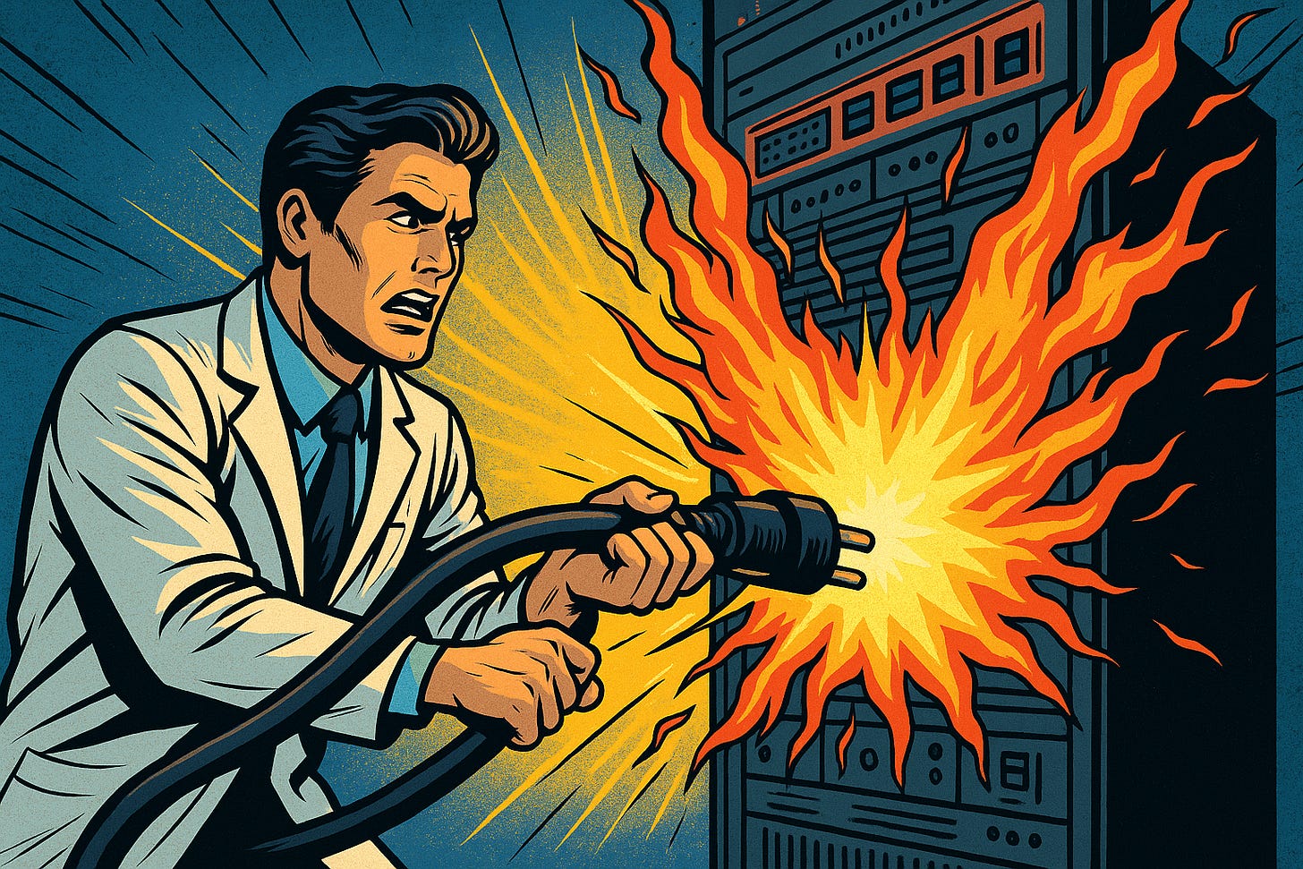
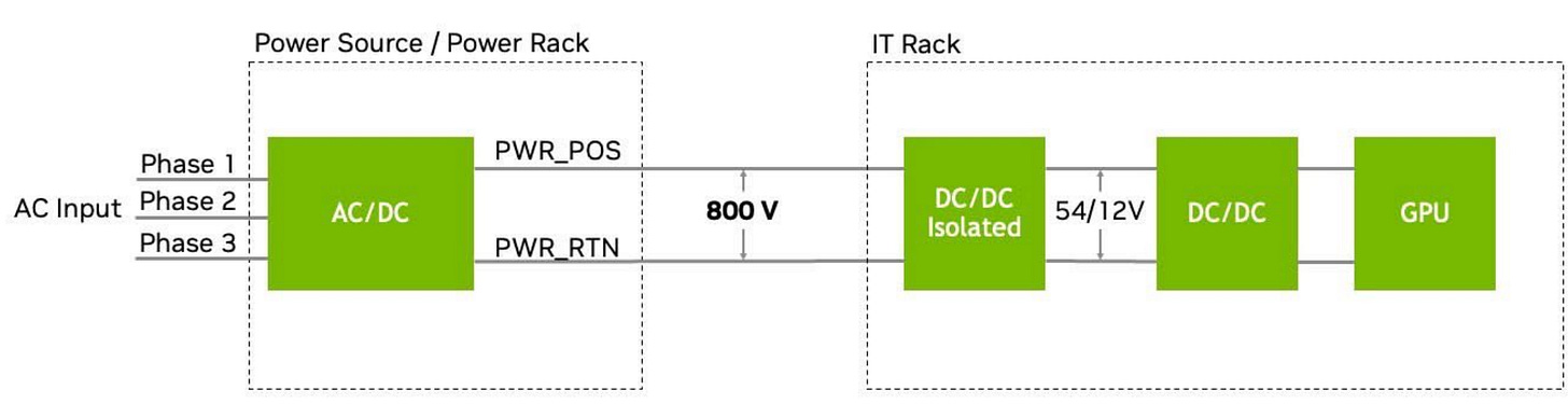
As AI workloads continue to grow exponentially, data center power requirements are rapidly escalating from hundreds of kilowatts to megawatt‑level per rack. Traditional54 V in‑rack power distribution, designed for ~kW racks, reaches its physical and efficiency limits once per‑rack delivery nears~200 kW, encountering issues such as bulky copper busbars, space constraints, and cumulative losses from multiple AC/DC and DC/DC conversions. NVIDIA’s emerging800 V HVDCarchitecture addresses these challenges by converting13.8 kV AC at the facility edgeinto800 V DC, which is then delivered via high‑current busbars directly to compute racks. Within each rack, only a single DC/DC stage is required to step down to 54 V or 12 V for GPU core voltages. This streamlined design reduces in‑rack copper usage by up to45 %, slashes conversion losses, frees up rack space, and lowers cooling overhead. When paired with optimized liquid cooling and centralized power conversion strategies, overall power delivery efficiency improves by approximately5 %, marking a paradigm shift in enabling1 MW‑class racksand beyond.
Supply Chain & Ecosystem
To accelerate this transition, NVIDIA has aligned with a cross‑section of industry partners across the AI power ecosystem. This includes power‑semiconductor leaders such asAnalog Devices, Infineon, Navitas, ROHM, STMicroelectronics, Renesas, Texas Instruments, who are developing the GaN‑/SiC‑based switches and control ICs at the heart of the 800 V HVDC lodestar. Supporting these silicon efforts are module and system vendors likeDelta, Flex Power, Lead Wealth, LiteOn, Megmeet, which design high‑voltage DC buses, rectifier units, and busbar assemblies. At the facilities layer, firms includingEaton, Schneider Electric, Vertivare collaborating on DC‑centric power rooms, overcurrent protection schemes, and integrated UPS/PDU systems. Together, this ecosystem is addressing safety, fault isolation, thermal management, and repair standards required to make high‑voltage DC viable at scale. With theNVIDIA Kyber rack platform slated for production in 2027, this ecosystem is expected to deliver a full stack, MW‑scale AI data center power architecture.
NVIDIA 800 VDC Architecture Will Power the Next Generation of AI Factories
However, inside an AI chip, the operating voltage (VDD) of CMOS logic is only around 0.6–1.0 V, with threshold voltages (Vt) even below 0.8 V. Converting 800 V down to sub‑1 V in a safe, efficient, and low‑noise manner is a fundamental system challenge. This is whereIVR (Integrated Voltage Regulator)technology becomes essential: IVRs move traditional board‑level VRMs into the package or even onto the die, delivering ultra‑stable power at very short distances, lowering PDN impedance, and enabling dynamic voltage scaling (DVS) to handle the large transient currents of AI workloads. This power chain—from HVDC to busbars, IVRs, and finally sub‑1 V CMOS—is the backbone of modern AI supercomputers. Without it, large‑scale AI clusters cannot operate reliably or efficiently.

Even once power delivery is stabilized, system design challenges continue. High‑density GPU motherboards must carry hundreds of high‑speed SerDes lanes and HBM memory interfaces, making theCCL (Copper‑Clad Laminate)materials of the PCB critical for signal integrity and system reliability. AI server boards often exceed 20–36 layers and must employ ultra‑low‑loss materials with low dielectric constants (Dk ≈ 3.2–3.5) and low dissipation factors (Df < 0.002), such asMegtron‑6orRogers 4350B, combined with heavy‑copper stack‑ups to sustain hundreds of amps of current and withstand tens of kilowatts of thermal load. Poor material selection or stack‑up design can lead to excessive insertion loss, eye‑diagram collapse, or board overheating, reducing long‑term reliability. Additionally, liquid‑cooling systems—whether direct‑to‑chip or full immersion—must be co‑designed with PCB stack‑ups, thermal interface materials, and rack‑level fluid loops to effectively dissipate heat. Only by integrating power delivery, PCB material design, thermal architecture, and high‑speed networking (such as NVLink or InfiniBand) can an AI data center achieve a truly scalable, high‑performance system. From wafer fabrication, advanced packaging (TSMC, Amkor, SPIL), testing, and module assembly to rack integration, building an AI supercomputer is a long and highly complex end‑to‑end process—every stage impacts overall efficiency and scalability, fully reflecting the precision and challenge of AI data center engineering.
In high-speedSerDesdesign, CCL (Copper-Clad Laminate) materials pose significant challenges to both Signal Integrity (SI) and Power Integrity (PI). Therefore, when evaluating and interpreting SerDes performance, it is essential to fully understand the material characteristics and their impact on channel loss.
In today’s high-speed digital system design, Signal Integrity (SI) and Power Integrity (PI) have become core factors influencing overall system performance and stability.
As SerDes (Serializer/Deserializer) channel rates evolve from 56G PAM4 to 112G, 224G, and even 400G PAM6, the effects of channel loss, crosstalk, reflections, and power noise on system Bit Error Rate (BER) and jitter are greatly amplified. Against this backdrop, CCL (Copper-Clad Laminate) materials play a critical role. They not only determine the insertion loss and overall performance of high-speed channels but also directly influence the impedance stability and thermal management of the PCB, serving as the critical bridge that links SI and PI considerations in next-generation SerDes design.
2025年7月8日
In our previous discussion, we explored in depth the critical role of Signal Integrity (SI) and Power Integrity (PI) in advanced AI chip design. These topics span not only the design of high-speed SerDes channels but also extend to the entire system-level Power Delivery Network (PDN) and signal transmission architecture.
For AI chips, where computational density, power consumption, and bandwidth requirements all surge simultaneously, any degradation in SI or PI directly leads to system performance bottlenecks, increased Bit Error Rate (BER), and even limits the scalability of the chip architecture.
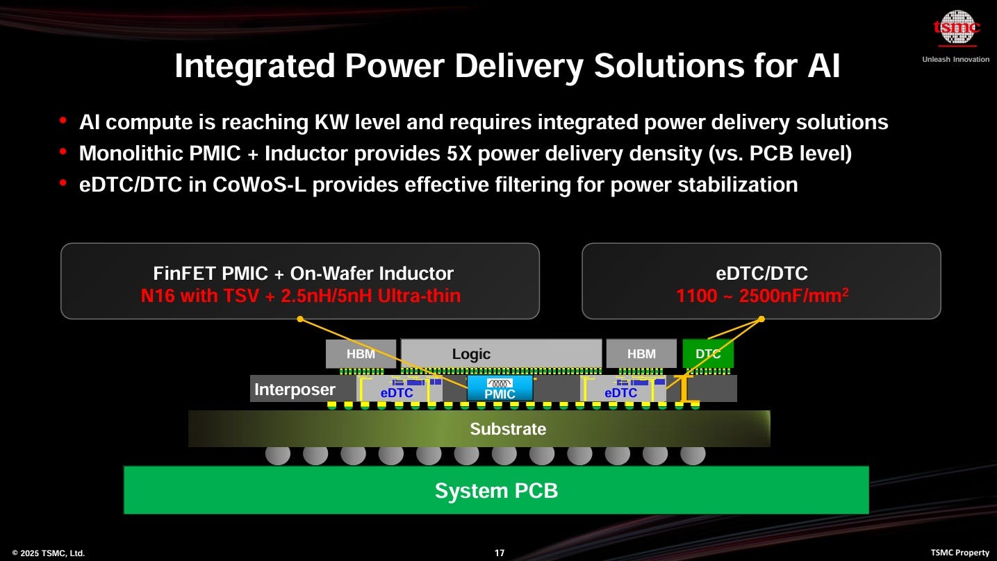
TSMC’s advanced CoWoS platform has already begun incorporatingIntegrated Voltage Regulator (IVR)technology, embedding voltage regulators directly into the package or chip. This approach, combined with high-performance Power Management ICs (PMICs) and precisely designed RF inductors, helps reduce power loop inductance, improve transient response, and suppress voltage ripple. At the same time, designers must account for effects such as the Q Factor to prevent resonances within the package from degrading high-speed power delivery. This level of fine-grained power integrity management is particularly critical for AI chips targeting large-scale training and inference workloads, where both SI and PI define the practical performance limits of next-generation data center systems.
Marvell’sPackage-Integrated Voltage Regulator (PIVR) technology, introduced in 2025, is a critical solution to the power delivery challenges faced by high-power AI and cloud data center chips. As AI processors surpass the multi-kilowatt power range, traditional board-level power delivery architectures encounter severe bottlenecks: long high-current, low-voltage paths, significant IR losses, slow transient response, and difficult-to-manage power noise. PIVR addresses these issues by integrating the voltage regulator directly into the chip package, minimizing power delivery distance, dramatically reducing parasitic inductance and voltage drop, improving IR losses by up to 85%, and lowering power loop noise by roughly 60%. This proximity-based power delivery method not only enhances transient response but also supports high-performance server platforms exceeding 4 kW, making it essential for high-speed SerDes, CXL, and optical-electrical co-packaged architectures.
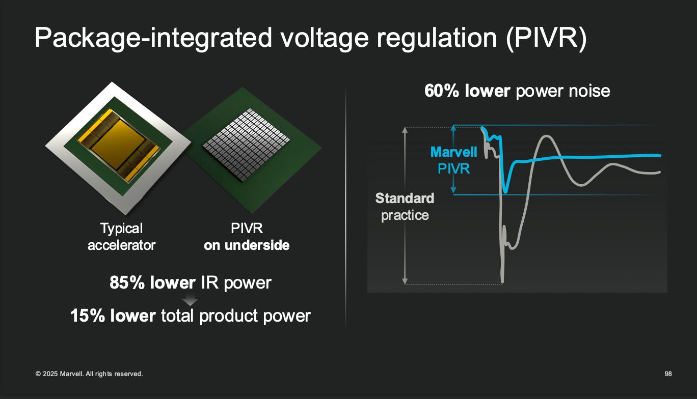
Marvell’sPIVR(Package-Integrated Voltage Regulator) technology combines high-performance PMICs, ultra-thin ferrite inductors, and precise power filtering control, achieving current densities of 3–4 A/mm²—significantly higher than the 1.5–2 A/mm² typical of traditional solutions—while supporting real-time voltage regulation to reduce overall power consumption by roughly 15%. To accomplish this, Marvell has built a complete package-level power delivery ecosystem in collaboration with partners such as Ferric, Empower, and Infineon. Ferric’s ultra-compact thin-film magnetic IVR modules are only one-tenth the volume of conventional solutions, making them ideal for direct package embedding and drastically reducing parasitic effects. Empower’s FinFast architecture provides fast dynamic power control, further improving transient stability. Together, these innovations not only enhance power integrity (PI) by minimizing loop inductance and mitigating Q-factor resonance risks but also directly benefit signal integrity (SI), as cleaner and more stable power delivery reduces jitter and power-induced noise that can degrade SerDes eye openings and increase bit error rates (BER).
In practical applications, Marvell’s PIVR (Package-Integrated Voltage Regulator) technology is particularly critical for CoWoS, chiplet-based architectures, and Co-Packaged Optics (CPO) systems, where ultra-high-speed channels and low-noise power delivery are essential. Traditional board-level power architectures not only increase the burden of PCB decoupling capacitors, loop design, and thermal management but also limit the scalability of advanced AI chip architectures. By embedding IVRs directly into the package, PIVR frees valuable PCB space, simplifies power distribution network (PDN) design, and provides a superior power solution for next-generation high-density multi-chiplet systems. For AI training and inference servers, as well as cloud data center platforms that demand extreme performance and energy efficiency, Marvell’s PIVR technology represents not just an innovation in power delivery design but also a core strategy for maintaining the overall balance of signal integrity (SI) and power integrity (PI).
Extending this concept further, the same design philosophy applies to Silicon Photonics (SiPh) platforms and Optical Engine architectures. At the2025 VLSI Symposium, TSMC introduced a comprehensive silicon photonics integration framework, where Photonic Integrated Circuits (PICs) and Electronic Integrated Circuits (EICs) are co-designed at the packaging level with holistic consideration of power delivery, thermal management, and signal interconnect performance. Since optoelectronic hybrid systems in 2.5D and 3D packages still rely on short- or medium-reach SerDes and high-speed channels to interface with the PCB, ensuring end-to-end channel consistency—from chip to package to board—has become a critical challenge for next-generation AI and data center system design.

2025年6月25日
Ultimately, whether it involves logic chips, photonic engines, or stacked HBM memory, all signal and power paths must eventually traverse the PCB, making high-speed PCB design principles indispensable. This trend underpins the industry’s growing focus on advanced packaging-to-board integration strategies such asCoWoP(Chip-on-Wafer-on-PCB), combined with fine-line manufacturing processes like mSAP (Modified Semi-Additive Process), to shorten interconnect lengths and optimize overall system performance.

In the semiconductor world, a silent yet dramatic revolution is underway. As process nodes push into 3 nm and 2 nm, the true limits of chips are no longer defined solely by lithography resolution, but by the complex trade‑offs of economics, power, and system‑level design. The giants of the AI era—large language models, generative AI accelerators, and 1.6 Tbps high‑speed interconnects—are devouring the advantages of traditional monolithic SoC designs, forcing the industry to fully embrace chiplets, Co‑Packaged Optics (CPO), and 3D integration throughhybrid bonding.
Tomorrow’s computing systems will no longer be single, monolithic engines. Instead, they will become intelligent infrastructures woven together by countless high‑speed chiplets, optical fibers, power delivery networks, and advanced cooling structures. At the heart of this transformation,CCL materials, PCBs, and advanced packaging (CoWoS, CoPoS, CoWoP)play a pivotal role. They not only determine signal transmission loss and integrity (SI) but also dictate power network stability and transient response (PI). Balancing multi‑layer high‑speed routing, complex PDNs, thermal management, and mechanical stress is now the core challenge for designers.
From Broadcom’s 224 G SerDes and Tomahawk 6, to Marvell’s PIVR power strategy, to MediaTek’s NVLink Fusion collaboration with NVIDIA—every step pushes the boundaries of extreme engineering and rewrites the philosophy of data center design. WhenCCL, PCB, CoWoS, CoPoS, CoWoP, SI, and PIall converge into a single design equation, the players who can find the perfect balance among power, bandwidth, materials, and ecosystem integration will ultimately define the winners of the AI era.
If you want to truly understand this deep transformation—spanning chips, packaging, and systems—and how top companies are shaping the semiconductor landscape for the next decade, this is content you simply cannot afford to miss.
For Paid Members ,SemiVision will discuss topics on
From 800 V to 0.8 V: Engineering the Next‑Generation AI Data Center
Powering the AI Era: From Grid‑Level HVDC to Sub‑Volt Silicon
Breaking the Bandwidth Barrier: How CCL and IVR Redefine SI/PI for 224G SerDes and PCIe 7.0
Challenges of PI/SI in High-Speed Transmission: The Evolution of PCB in the SerDes Era
Market Implications in Nvidia’s AI GPU
PI/SI Design Challenges under Rising SerDes Bandwidth
Signal Integrity (SI) Challenges
Power Integrity (PI) Challenges
System-Level Challenges of SerDes Bandwidth Scaling
Summary and Industry Implications
Upstream Material Segment – CCL and Electronic Glass Fabric
PCB Manufacturing – Advanced Processes and System Co-Design
A Value Chain Reshaped by AI Compute Demand
Resonance and Impedance Traps in Power Integrity: Rethinking “Lower Impedance Is Always Better”
The Physical Nature of Resonance
Quality Factor (Q-Factor) and Impedance Peaks
CCL Materials and Signal/Power Integrity Challenges in High-Speed SerDes Design
PCB CCL Materials and Channel Loss
PAM4 and PCIe Gen6 Channel Loss
Enterprise Strategies in High‑Speed Connectivity: Broadcom, Marvell, and MediaTek
Industry Update: Marvell
Industry Update: Broadcom
Industry Update: MediaTek
Impact of Integrated Voltage Regulators (IVR) on SI/PI
From 800 V to 0.8 V: Engineering the Next‑Generation AI Data Center
When building a modern AI data center, it is essential to master power architecture, thermal solutions, and AI clusterscale‑outcapabilities to create a high‑efficiency, continuously expandable computing platform. In recent years, leading data center designs have adopted800 V HVDC (High‑Voltage Direct Current)rack‑level power distribution, delivering medium‑voltage DC directly to each rack. This approach significantly reduces transmission current, saves over 45% of copper usage, and minimizes multi‑stage conversion losses, improving overall system efficiency by nearly five times. However, for chips such as AI GPUs and accelerators, the internal CMOS core voltage (VDD) is only about 0.6–1.0 V, with threshold voltages (Vt) often below 0.8 V. Efficiently, safely, and quietly stepping down 800 V to sub‑1 V levels is one of the most critical challenges in system design. This need has driven the widespread adoption ofIVRs (Integrated Voltage Regulators), which perform local voltage conversion and regulation within the package or even directly on the die. IVRs reduce PDN impedance, support high‑speedDynamic Voltage Scaling (DVS), and ensure AI chips remain stable under extreme transient current spikes. Commercial solutions such asEmpower EP71xxandMarvell PIVRhave already entered the market, integrating directly into GPU or AI accelerator power modules, forming the backbone of modern AI supercomputers.
Once the power delivery network is stabilized, designers must tackle high‑speed signaling and system reliability challenges, makingCCL (Copper‑Clad Laminate)PCB base materials mission‑critical. AI server motherboards often use 20–36‑layer high‑density PCBs that must simultaneously handle high‑speed SerDes interfaces (112G–224G PAM4), hundreds of amps of current, and multi‑kilowatt thermal loads. This demandsultra‑low‑loss, low‑Dk/Df, high‑Tg, heavy‑copper materialssuch asMegtron‑6,Rogers 4350B, or equivalent. Poor material selection or stack‑up design can lead to increased insertion loss, eye‑diagram collapse, or overheating that shortens board lifespan. In parallel,direct‑to‑chiporimmersion liquid coolingsystems, along with carefully engineered thermal interface materials, must be co‑designed with the PCB stack and rack fluid loops to efficiently dissipate tens of kilowatts of heat. Building an AI supercomputer—from wafer fabrication, advanced packaging (TSMC, Amkor, SPIL), testing, and PCB assembly to full system integration—is a long and complex end‑to‑end process. Every stage affects overall performance, energy efficiency, and scalability, illustrating the high precision and complexity inherent in AI data center engineering.
System Power & Integration Flow:
AC Grid (13.8 kV)→800 V DC rectifier rack→1 MW HVDC busbar to each rack→IVR / PCB VRM → 0.6–1 V CMOS power→Heavy‑copper PSU PDN (millimeter‑scale)→High‑frequency, low‑loss PCB (Megtron‑6 / Rogers, etc.)→GPU / CPU with direct liquid or immersion cooling→NVLink / InfiniBand high‑speed network for scale‑out clusters→Software and management platform integration
Powering the AI Era: From Grid‑Level HVDC to Sub‑Volt Silicon
- 800 V HVDC Power System: An Energy‑Efficiency Revolution from Grid to AI Racks
State‑of‑the‑art AI data centers are rapidly transitioning from traditional 415 V AC / 48–54 V DC power distribution to 800 V HVDC (High‑Voltage Direct Current) architectures. By converting 13.8 kV AC grid power directly to 800 V DC at the facility perimeter and delivering it to compute racks, the system eliminates multiple AC/DC stages. This approach reduces in‑rack copper usage by over 45%, lowers multi‑stage conversion losses, and improves overall end‑to‑end power efficiency by approximately 5%.
For example, NVIDIA is working with key power semiconductor partners, including Texas Instruments, to develop 1 MW‑per‑rack AI power architectures that leverage low‑inductance laminated busbars, GaN/SiC rectifiers, and high‑current dual‑pole DC bus configurations to minimize transmission losses and maximize power density.
This evolution reduces cabling and cost, shortens conductor paths to mitigate EMI, and—when paired with optimized liquid cooling and facility‑level DC distribution—can help large‑scale AI data centers achieve PUE levels approaching 1.05–1.10.
- Bridging 800 V to 0.8 V CMOS: IVR as the Key to Power Efficiency
In modern AI GPUs and specialized accelerators, core supply voltages (VDD) typically range from0.6–0.9 V, peaking around 1.0 V under heavy load, while advanced‑node threshold voltages (Vt) are often as low as0.2–0.4 V. Excess voltage can induce reliability issues such as hot carrier injection (HCI) or bias temperature instability (BTI), whereas insufficient voltage risks timing violations and computation errors. Precise sub‑volt power delivery with fast transient response is therefore critical for high‑performance AI silicon.
-
Integrated Voltage Regulators (IVRs)relocate traditional PCB‑level voltage regulation modules (VRMs) into the package or even on‑die. This near‑chip delivery architecture shortens the power path to just a few millimeters, achieving milliohm‑level PDN (Power Delivery Network) impedance and supporting massive transient currents during tensor workloads. IVRs also enable rapid Dynamic Voltage and Frequency Scaling (DVFS/DVS), boosting voltage during intensive compute bursts and lowering it in idle states to reduce total power and thermal load. For example,Empower Semiconductor’s EP71xx series IVRsprovide multi‑channel outputs with static power consumption of only a few milliwatts, underscoring their role as a core enabler for next‑generation AI supercomputers.
-
Signal Integrity and CCL Material: Engineering the PCB Backbone
Modern AI servers carry hundreds of SerDes lanes running at 30–112 Gbps for 800 G Ethernet, PCIe 6.0, and HBM4 interconnects. The PCB’s Copper‑Clad Laminate (CCL) material is therefore mission‑critical, requiring:
Low dielectric constant (Dk ≈ 3–4)
Ultra‑low dissipation factor (Df < 0.002)
High glass transition temperature (Tg ≥ 180 ℃)
Heavy copper layers to sustain both high current and thermal loads
High‑speed laminates likeMegtron‑6(εr≈3.4@GHz, Df≈0.002) support 24‑36‑layer stack‑ups, improving signal integrity. Heavy‑copper boards (≥ 4 oz per layer) can deliver 50–500 A per trace. Using lower‑grade materials risks insertion loss, jitter, eye‑diagram collapse, or thermal failures.
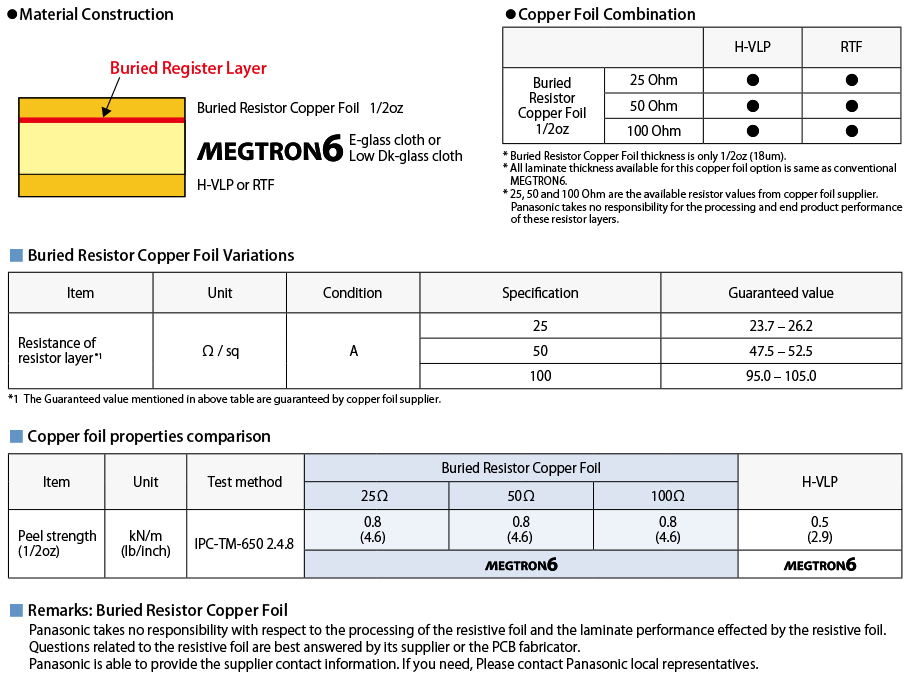
PCB fabrication complexity—SOP/OOP spacing, drilling tolerances, lamination cycles, and Tg durability—requires early co‑design with board manufacturers to ensure stack‑up reliability.
- Liquid Cooling for High‑Density Thermal Loads
Modern AI racks are reaching80–120 kW per rack, as GPUs likeNVIDIA BlackwellandAMD MI300Xapproach600–1,000 W per device. Once racks exceed30–40 kW, air cooling becomes impractical, and liquid cooling—eitherDirect‑to‑Chip (D2C)orimmersion—is mandatory.
For example,TensorWave’s 8,192‑GPU clusterbased on next‑generation AMD MI3xx series sustains60–100 kW per rackusing direct liquid cooling.
Vendors such asSupermicro, Flex, and Aivresnow providefully integrated liquid‑cooled racks (pPUE ≤ 1.06), pre‑assembled with rack‑level manifolds, heat exchangers, and cold plates, enablingdeployment in 3–6 months.
- AI Cluster Architecture and Scale‑Out Strategy
AI training clusters typically adoptscale‑out distributed topologies, leveraging high‑bandwidth fabrics such asInfiniBand and NVLink/NVSwitchto form massive training pools and avoid single‑node bottlenecks.
For example,NVIDIA NVL72 and NVL144systems illustrate the scaling challenge: as GPU counts grow from 72 to 144, the complexity ofpower distribution, signal routing, and thermal managementincreases non‑linearly. These systems requiremulti‑rail power delivery, synchronized timing, and precise clock‑skew managementto maintain reliable large‑scale training.
Achieving true cluster performance gains demands a careful balance betweenscale‑up within each rack—via dense NVLink/NVSwitch interconnects—andscale‑out across the network fabric, ensuring data consistency and throughput at the scale of thousands of GPUs.
- From AI Chip Fabrication to Full System Deployment
The lifecycle fromwafer fabrication → wafer test → advanced packaging (e.g., TSMC CoWoS / SiP, Amkor, SPIL) → system assembly → data center deploymentinvolves extensive reliability and validation at each stage. Dynamic tuning of power, thermal, and signal conditions is required to meet real‑world operational limits.
TSMC’s2 nmchips, expected for mass production in 2026, combined withHBM4 integration and on‑package IVR, will further improve AI data center performance and energy efficiency.
Breaking the Bandwidth Barrier: How CCL and IVR Redefine SI/PI for 224G SerDes and PCIe 7.0
The first step in high-speed PCB design is understanding the sources and characteristics of channel loss. For SerDes, channel loss can be classified into two main categories:conductor lossanddielectric loss. Conductor loss is primarily determined by the surface roughness of the copper foil (Ra/Rz) and the skin effect at high frequencies, while dielectric loss is dominated by the core and prepreg CCL properties—specifically the dielectric constant (Dk) and dissipation factor (Df).
Once the operating frequency reaches 28 GHz and above, even subtle material non-uniformities, fiber weave effects, or power noise can become critical bottlenecks to signal integrity. This is why recent high-speed PCB design trends have focused onUltra-Low Loss (ULL)andExtreme Low Loss (ELL)materials, featuring resin systems withDf ≤ 0.005andDk ≤ 3.3, as well as advanced copper foils such asHVLP4~5 (highly smooth copper)combined with second- and third-generation low-loss glass fabrics.
These optimizations collectively reduce insertion loss, minimize mode conversion, and enhance overall channel performance, which are essential for enabling 112G PAM4, 224G SerDes, and future AI/HPC optical-electrical hybrid interconnects.
For system designers, interpreting SerDes performance goes far beyond examining eye diagrams or TDR (Time Domain Reflectometry) test results. The key lies in performing asystem-level analysisthat encompasses material selection, stack-up configuration, impedance control, and power delivery design. In other words, understanding the impact of CCL materials on SI (Signal Integrity) and PI (Power Integrity) in high-speed transmission is fundamentally about grasping thephysical foundations of SerDes channel performance. Only by tightly integrating material selection, PCB design, and the requirements of high-speed modules—such as 224G PAM4 or 1.6T/3.2T switches—can designers gain a true competitive edge in next-generation AI and HPC interconnects.
In modern high-speed system design, as AI/HPC servers, data center switches, and accelerator cards continue to scale in performance,signal integrity (SI)andpower integrity (PI)have emerged as the two core challenges that determine design success. SerDes (Serializer/Deserializer) technology, as the backbone of high-speed connectivity, is rapidly advancing fromPCIe 5.0 (32 GT/s)toPCIe 6.0 (64 GT/s PAM4)andPCIe 7.0 (128 GT/s PAM4), while also enabling56G, 112G, and 224G PAM4SerDes to become the primary interconnect solutions for data centers, CXL 3.0/4.0, and AI chip-to-chip links.
This leap in signaling rates dramatically amplifies the effects ofchannel loss, crosstalk, reflections, and power noiseon BER (Bit Error Rate) and eye diagram performance. Consequently,material engineering, PCB design strategies, and power delivery managementmust evolve in parallel to meet the stringent requirements of next-generation high-speed systems.
In high-speed SerDes design, the selection of PCBCCL (Copper-Clad Laminate)materials is acritical factoraffecting bothsignal integrity (SI)andpower integrity (PI). Channel loss primarily originates from two sources:conductor lossanddielectric loss. Conductor loss is proportional to copper surface roughness (Ra/Rz) and theskin effectat high frequencies, while dielectric loss is determined by thedielectric constant (Dk)anddissipation factor (Df)of the laminate.
As PCIe and SerDes operating frequencies enter the28 GHz to 64 GHz range and beyond, even subtle variations in material properties,fiber weave effects, or transient power fluctuations can directly degrade channel BER (Bit Error Rate). This is why modern high-speed PCB design is rapidly moving towardUltra-Low Loss (ULL)andExtreme Low Loss (ELL)materials—for example, resin systems withDf ≤ 0.005andDk ≤ 3.3, second-generation low-loss or quartz glass fabrics, andHVLP4–5 smooth copper foils—to minimize channel loss and ensure robust signal integrity for1.6T / 3.2T switches and PCIe 7.0 systems.
However, simply optimizing the channel itself is not sufficient to ensure overall system stability. As SerDes speeds continue to rise,power noise couplinghas an increasingly significant impact onsignal integrity (SI). This is where the role of theIntegrated Voltage Regulator (IVR)becomes critical. Traditionalboard-level VRMs (Voltage Regulator Modules)struggle to handle high-speed load transients and rapid current switching, which leads to voltage droop and jitter propagating into SerDes channels, degrading eye openings and increasing BER.
By integrating voltage regulation directly into the chip or package,IVRssignificantly shorten the power delivery path, reducing theparasitic inductance and impedanceof thePower Delivery Network (PDN). This mitigates transient voltage fluctuations during high-speed load switching and enables SerDes to operate in ultra-low jitter environments. ForPCIe 6.0/7.0 and 224G PAM4 designs, IVRs not only enhance transient response but also improve the overallSI/PI coupling performance, making them one of the essential solutions for next-generation high-speed systems.
In summary, as PCIe and SerDes data rates continue to climb,CCL material selection, PCB stack-up, IVR architecture, and PDN designmust form a tightly integratedecosystem loop. Only by simultaneously masteringUltra-Low Loss material engineering,SerDes channel loss control, andIVR-based transient power managementcan designers achieve stable signal transmission and superior system performance in next-generationAI/HPC platforms, CXL-based expansions, and ultra-high-bandwidth data centers.
Challenges of PI/SI in High-Speed Transmission: The Evolution of PCB in the SerDes Era
With the rapid growth ofAI, big data, and cloud computing, AI servers and data centers have become the fastest-growing sectors driving downstream PCB demand. According to Prismark, the PCB market share for servers and data storage is projected to rise from10% in 2024to19% in 2028, reflecting the accelerating demand for high-end PCBs to support high-performance computing. As AI servers transition from traditional CPU-based architectures to GPU-centric systems,routing densityandhigh-speed signal transmission capabilitybecome the primary design drivers. This shift imposes unprecedented challenges onPCB layer count, material selection, and manufacturing processes, directly propelling the rapid evolution of upstreamCCL (Copper-Clad Laminate)andelectronic glass fiber fabrics.
In high-speedSerDes architectures,signal integrity (SI)andpower integrity (PI)are the core design challenges. AI server motherboards and 800G switch PCBs have already increased from14–24 layers to 20–30 layers, fully adoptingHigh-Density Interconnect (HDI)andmSAP (Modified Semi-Additive Process)technologies to support20/20 µm line/spaceand complex routing schemes. Such high-layer-count designs result in thicker boards and more complicated via structures, which not only increase the risk ofskewed drilling, burrs, and interlayer misalignment, but also impose extreme requirements onlamination, drilling, and plating processes. Particularly for800G and 1.6T networking equipment, any signal loss or impedance discontinuity can lead toeye diagram closureandBER degradation, making SI simulation and process control more critical than ever.
On thematerialsside, high-speed transmission imposesstricter dielectric constant (Dk) and dissipation factor (Df)requirements. Signal speed and integrity are highly dependent on the dielectric performance of the CCL, in whichelectronic glass fabrics are the decisive factor. Driven by the computing demands ofNVIDIA’s GB200 and upcoming GB300 GPUs, motherboards and switches are now widely adoptingM8-grade low-Dk glass fabricsandultra-low-loss CCLs. Looking ahead to 2026,1.6T switches and high-end serverswill enter theM9 generation, whereDf levels must reach 0.0007 (7×10⁻⁴). This trend will pushAsahi Kasei’s Q-Glass (quartz glass fabrics)toward becoming the mainstream material choice. Despite itshigher cost and greater processing difficulty, itssuperior electrical performanceprovides a clear competitive advantage for next-generation AI/HPC high-speed systems.
In recent years,electronic-grade glass fiberhas become increasingly critical in PCB laminates forhigh-speed servers and switches, especially under the demands ofAI data centers and high-frequency, high-speed transmission. The technology roadmap for thenext-generation low-loss CCL (Copper-Clad Laminate)is rapidly evolving, as glass fiber is one of its core raw materials. A CCL consists ofglass fabric, resin, and copper foil, withglass fabric directly determining the dielectric properties and thermal stabilityof the laminate.
The current highest-grade CCL isM8, supporting112G/224G PAM4and1.6T-class switches, while thenext-generation M9 CCLis expected to entermass production in late 2026. It will be primarily used in:
NVIDIA Kyber / NVL288rack orthogonal backplanes
Google TPU V7andAWS Tranium 3server PCBs
1.6T-class Ethernet switch motherboards
M9-grade CCLstypically adopt aPPO (polyphenylene oxide) resin system, combined withHVLP4 or HVLP5 ultra-low-roughness copper foil, and reinforced withnext-generation NEZ Glass or Q Glass fabrics.
Performance evaluation for electronic-grade glass fiber focuses on three key indicators:
CTE (Coefficient of Thermal Expansion)– Impacts thermal reliability and warpage.
Dk (Dielectric Constant)– Affects signal speed and impedance control.
Df (Dissipation Factor)– Dominates signal attenuation at high frequencies.
Among these,Df is the most critical factor for high-speed signal integrity, making it the primary threshold for M9-grade laminates.
From the material evolution perspective:
Nittobohas advanced from1st-gen NE Glassto2nd-gen NER Glass, and now to3rd-gen NEZ Glass, continuously optimizing Dk and Df byadjusting the SiO₂ and B₂O₃ ratios.
Asahi Kasei, on the other hand, is pursuing a fullQ Glass (quartz glass)strategy, replacing traditional glass fibers with99.9% high-purity quartzto achieve:
Ultra-low CTE (~0.5 ppm/°C)
Low Dk (~3.7)
Extreme low Df (~0.0005), approaching the theoretical limit of glass fiber.
In fact,pure quartz fabricscan achieveDf ~0.0002under optimal processing.
Despite its superior performance,Q Glass faces two major challenges:
Processing difficulty– The extreme hardness of quartz causesfiber residue during PCB drilling, which can compromise copper plating quality.Special coated drill bitsare required.
High cost– At$50 per meter, Q Glass is~1.7–2× more expensivethan NEZ Glass.
Nonetheless,high-end AI servers are less cost-sensitive, and withM9 demanding Df ≤ 0.0007,Q Glass is highly likely to become the mainstream choice.
This transition also drivessupply chain ripple effects:
NEZ Glassis currently supplied only byNittobo (Japan)andAGY (USA)for the highest-grade fibers.
Q Glass, by contrast, hasbroader raw material availability, andTaiwanese and Chinese manufacturersare now entering the market, helpingCCL suppliers reduce risk and avoid shortages.
Thehigh hardness of quartzalsodramatically shortens drill bit lifespan—from1,000 holes on M7 laminates to only ~200 holes on M9—spurring demand forpremium coated drill bits, such asUnion Tool ULF and DC series, which are specifically designed for PCBs containing quartz fabrics.
High-speed SerDes interfaces posedirect challenges to PI (Power Integrity) and SI (Signal Integrity). Aslink bandwidth increasesandchannel counts grow, maintainingpower network noise suppression and impedance controlbecomes significantly more difficult.
Inhigh-layer-count PCBs, dielectric layers arethinner, and the spacing between power planes isnarrower. Under such conditions:
Local parasitic inductance
Uneven capacitance distribution
Discontinuous return paths
can all causetarget impedance deviationandtransient voltage droop (AC droop). This directly impactshigh-speed SerDes jitterandeye diagram opening, increasing the risk ofbit errors.
This means thatPI and SI must be treated as a co-optimized system problem. Achieving stability at112G/224G PAM4 or PCIe 6.0/7.0speeds requiresend-to-end optimization, covering:
Material selection– Ultra-low-loss (ULL) and extreme-low-loss (ELL) CCLs with controlled Dk/Df.
Stack-up design– Minimized loop inductance and consistent return paths.
Via planning– Optimized for signal return and reduced impedance discontinuity.
mSAP micro-trace processing– Supporting fine line/space (≤20/20 µm) for high-density routing.
Market Implications in NVIDIA’s AI GPU
As NVIDIA’s next‑generation AI GPU platforms reach the market, the demand for advanced PCBs and substrate materials is accelerating. GPU server motherboards, interposers, and high‑speed switch boards all require complex multi‑layer designs with stringent signal‑integrity and power‑delivery performance.
For the PCB and materials industry, this is not only a high‑growth opportunity but also a full‑spectrum engineering challenge, spanningpower‑integrity and signal‑integrity co‑design, high‑speed SerDes channel engineering, and next‑generation manufacturing capabilities. Companies capable of optimizing design, material, and fabrication in an integrated workflow will hold a decisive advantage in the era of AI‑driven data centers.
PI/SI Design Challenges under Rising SerDes Bandwidth
As the era of high-speed SerDes unfolds,servers and switchesare experiencing anexponential increase in link bandwidth. Ethernet links have evolved from400G to 800G, with1.6T systemsalready on the horizon. Modern architectures now rely on112G PAM4signaling and are moving toward224G PAM4, pushingNyquist frequencies to 56 GHz and 112 GHz. Each bandwidth leap imposesstricter requirementsonSignal Integrity (SI)andPower Integrity (PI)in PCB design.
Signal Integrity (SI) Challenges
Loss and Reflection
At 56–112 GHz, even smalldielectric losses,conductor losses, orimpedance discontinuitiescan causeeye diagram closureand asignificant BER increase.
Via Design and Backdrilling
High-layer-count PCBs mustminimize via parasitics.
Backdrillingis critical to suppress stub reflections, whiletight differential impedance controlis essential across layers.
Material Dielectric Limits
SerDes channels demandultra-low Dk/Df CCL materialsto maintain signal quality over long distances.
This drives the adoption ofM8 and next-generation M9 laminates, enabling sub-0.001 Df performance for 224G PAM4.
Power Integrity (PI) Challenges
Target Impedance Control
High-speed SerDes links areextremely sensitive to transient current response.
PDN design must ensurebroadband impedancestays below the target, or jitter and BER degradation will occur.
Return Path and Parasitic Inductance
Narrow spacing betweenpower and ground planesin multi-layer PCBs increases the risk ofAC droopandcommon-mode noiseif return paths are discontinuous or via inductance is not optimized.
Decoupling and Distributed Capacitance
Rising power density and transient currents requireoptimized MLCC placementcoordinated withfull-board PDN simulation.
Embedded capacitance layers or planar decouplingbecome necessary to suppress high-frequency noise.
System-Level Challenges of SerDes Bandwidth Scaling
Tighter Channel Loss Margins
224G PAM4 offersextremely low toleranceforInsertion Loss (IL)andReturn Loss (RL).
PCB manufacturing must implementmSAP fine-line processesandHVLP/ultra-smooth copper foilsto control channel loss.
Full-System PI/SI Co-Design
PI and SI can no longer be treated in isolation.
Designers must integratetime-domain target impedance analysis,high-speed channel simulations, andSSN (Simultaneous Switching Noise)modeling for board-level validation.
Stricter Manufacturing and Reliability Requirements
High-layer, high-density PCBs increase complexity inlamination, laser drilling, and copper plating.
Process variations directly affect SerDes channel performance, requiring asupply chain with deep process know-howto ensure yield and long-term reliability.
This evolution marks aparadigm shift in PCB design for AI/HPC systems, whereultra-low-loss materials, PI/SI co-optimization, and advanced manufacturing processesare all indispensable to sustaining next-generation 112G/224G SerDes links in1.6T+ networking and PCIe 7.0/CXL platforms.
In the high‑speed transmission era,Power Integrity (PI)andSignal Integrity (SI)have evolved beyond traditional, independent design flows. They now represent a holistic engineering challenge that spansmaterials, stack‑up architecture, manufacturing processes, simulation, and full system‑level co‑optimization. This shift not only determines the feasibility of ultra‑high‑speed SerDes but also directly impacts theperformance and reliabilityof AI servers and modern data centers.
Summary and Industry Implications
The rise of AI servers and high-speed data centers is fundamentally reshaping the entire value chain of PCB, CCL, and electronic-grade glass fiber fabrics. On the application side, GPU-centric AI servers are driving the rapid evolution ofhigh-layer-count, multi-stack, high-density interconnect (HDI)PCBs. SerDes bandwidth has moved from 56G to 112G and is now advancing toward224G and beyond, imposingsystem-level challengesfor bothSignal Integrity (SI)andPower Integrity (PI). This is no longer a pure board-level design problem but rather afull-chain engineering effortthat spansmaterials, manufacturing processes, and system co-design.
Upstream Material Segment – CCL and Electronic Glass Fabric
Electronic glass fabric determines the dielectric properties of CCL and is the key enabler for stable high-speed transmission. The market forlow-Dk and ultra-low-Dkglass fabrics is expanding rapidly, with traditional fabrics such asE-glass and NE-glasstransitioning towardhigh-performance quartz fabrics (Q Glass)andNEZ Glass, meeting the requirements ofM8 and upcoming M9-grade CCL.
CCL is theperformance foundationof high-speed PCBs. FromPanasonic Megtron 7 to Megtron 8, and soon Megtron 9, the continuous reduction inDf and Dkdirectly aligns with the mass production needs of800G, 1.6T, and even faster networking equipment. FutureM9-grade CCLproduction will be driven byquartz-based fabrics, significantly increasing both value density and technical barriers.。
PCB Manufacturing – Advanced Processes and System Co-Design
On the PCB manufacturing side,mSAP (modified Semi-Additive Process)andhigh-layer-count boardsare becoming mainstream, involving high-precision steps such asultra-thin copper control, laser microvia drilling, electroless copper plating, and precision lamination—all of which contribute to higher added value.
TakingNVIDIA’s GB200 seriesas an example, the 2025 market size for PCBs supportinghigh-end AI servers and 800G switchesalready exceeds26 billion, with thelow-Dk glass fabric segment surpassing 2 billion. With the upcoming1.6T switches and higher-power AI servers, these figures are expected to grow further.
A Value Chain Reshaped by AI Compute Demand
Downstream Applications (AI Servers & Switches)– Determine bandwidth and layer count, driving SerDes evolution and high-speed interconnect requirements.
Midstream PCB Manufacturing– Competitiveness will depend onhigh-layer HDI, mSAP precision, and PI/SI co-design capabilities.
Upstream Materials (CCL & Electronic Glass Fabric)–Ultra-low-Dk and ultra-low-Dfbecome the core direction, withquartz fabrics and advanced resin systemsas the critical enablers.
In this value chain,any bottleneck can constrain the expansion of AI infrastructure. The transition toM9-grade CCLandquartz-based electronic fabricsmagnifies the importance ofglobal supply chain layout and advanced process capabilities. In the coming high-speed interconnect era, companies that canintegrate material innovation, PCB manufacturing expertise, and PI/SI system-level co-designwill be best positioned to capture the growth dividend driven by AI.
Resonance and Impedance Traps in Power Integrity: Rethinking “Lower Impedance Is Always Better”
In the field ofPower Integrity (PI)design, we often follow an intuitive principle: thePower Delivery Network (PDN)should have the lowest possible impedance. The reasoning is simple—according to Ohm’s law, when transient current occurs, if the impedance is sufficiently low, even dramatic current changes will not cause voltage droop beyond the acceptable range.
However, this intuition overlookstwo critical issues:
PDN impedance does not decrease monotonically; it exhibits resonance behavior.
Transient current waveforms contain frequency components that may overlap with the resonant frequencies, triggering voltage oscillations.
In other words,the valleys or peaks in the impedance curve can hide catastrophic voltage fluctuations.
InPower Integrity (PI)design, while we instinctively believe that aPower Delivery Network (PDN)with lower impedance is always better—because according to Ohm’s law…
ΔV=Itransient×ZPDN
Lower impedance can reduce transient voltage droop, but this intuition overlooks two critical issues.
First, a practicalPower Delivery Network (PDN)is a complex RLC network composed of the VRM, PCB, package, on-chip power grid, and multiple stages of decoupling capacitors. Its impedance curve isnot monotonic; it exhibitsseries resonances(creating valleys) andparallel anti-resonances(creating sharp peaks).
Second, the transient current of a processor or AI accelerator containsrich frequency components. If these frequencies overlap with the PDN’s resonant frequencies, they can triggervoltage oscillations or rogue waves, leading to system instability.
In other words,simply chasing low impedance while ignoring resonance control and damping design—for example, through capacitor ESR distribution or hierarchical decoupling optimization—hides significant risks.
A truly robust PI design should maintainlow and smooth impedance across the entire frequency spectrum, avoiding high-Q resonances that can cause catastrophic voltage fluctuations.
The Physical Nature of Resonance
Resonanceis a phenomenon widely present in the physical world.
When a system is excited periodically, and the excitation frequency matches the system’snatural frequency, the system exhibits a dramatic response with rapidly increasing amplitude. This frequency is called theresonant frequency.
InPCB and PDN design,
Capacitance (C)stores electric energy
Inductance (L)stores magnetic energy
WhenL and C form a resonance, energy rapidly oscillates between the electric and magnetic fields.
If an external load current happens to excite this resonant mode, the voltage canswing violently, which is the root cause of the“rogue wave”phenomenon in PI design.
There aretwo primary types of PDN resonances:
Series Resonance– The impedance curve forms aV-shaped valley
Parallel Resonance– The impedance curve forms aninverted V-shaped peak
- Series and Parallel Resonance
Series Resonance
Consider aseries RLC circuit, where the total impedance is:
ZRLC=RDC+jωL+1jωC
When the inductive reactance equals the capacitive reactance (XL = XC), the circuit reaches theseries resonance point.
fr=12πLC
At this point, the overall reactance cancels out, and the system is left only with theDC resistance (R_DC), resulting in aV-shaped impedance curve.
Although the impedance is at its minimum—seemingly favorable for PI design—if the load current waveform contains components at this frequency, the system can experience severevoltage oscillations, representing a criticaldesign trap.
Characteristics:
Impedance islowestat the resonance point
Energy rapidly exchanges betweenLandC
A step-load excitation at this frequency can easily inducelarge voltage fluctuations
Parallel Resonance
Y=1R+1jωL+jωC
At the resonance point, the conditionX_L = X_Cis also satisfied, and the impedance exhibits ahigh peak (inverted V-shape):
fr=12πLC
Parallel resonance commonly occurs in theinterface regions of the PDN, such as:
The combination ofVRM and PCB MLCCs
Thecoupling effectsbetween the package and the silicon die
This type ofhigh-frequency parallel resonanceis the most dangerous, because it produces asharp impedance peak. Once the load current contains frequency components near this point, the voltage ripple will beamplified, forming a so-called“Rogue Wave.”
Quality Factor (Q-Factor) and Impedance Peaks
The severity of resonance is described by theQ-Factor, which is commonly defined in two ways:
Energy ratio definition:
(Energy stored / Energy dissipated per cycle)
Q=2πEstoredEdissipated/cycle
Frequency ratio definition:
(Resonant frequency / Bandwidth at −3 dB)
Q=frBW3dB
Ahigh Q-Factorindicates high energy storage efficiency and low loss, but it isdisastrous for PI design, because the impedance peak becomes sharp and energy is hard to dissipate; once excited, it leads to severe voltage oscillations.
Alow Q-Factorsystem dissipates energy quickly, resulting in a smoother impedance profile, which helps suppress voltage ripple.
In practical design, reducing the Q-Factor can be achieved by:
Introducing appropriateESRor damping resistors
Avoiding excessive MLCC parallelization, which can create ultra-high Q resonances
Controllingparasitic L and Cof the package and die in the high-frequency region
Implications for PI Design
Lower impedance is not always better— it is essential to avoid deep valleys or sharp peaks near the load’s operating frequencies.
Resonance frequency alignment with load spectrum is critical— most Rogue Waves are triggered by resonant excitation.
Controlling the Q-Factor is central to PI design— lower-Q systems are safer and more stable.
System simulation and spectral analysis must be combined— relying solely on target impedance is insufficient to guarantee stability.
In conclusion, a well-designed PDN features a smooth impedance profile with no sharp peaks and a moderate Q-Factor, rather than blindly pursuing ultra-low impedance across the entire frequency range. This principle is fundamental for power integrity in modern designs, from high-speed AI servers to HPC systems.
Based on current high‑frequency and high‑speed packaging and power delivery design principles, it is clear thatNVIDIA is aggressively addressing Power Delivery Network (PDN) challenges. At 224G SerDes, CXL 4.0, PCIe 7.0, and in 1.6T/3.2T optical engines and AI server environments,Power Integrity (PI)andSignal Integrity (SI)are tightly coupled—any transient voltage fluctuation can immediately manifest as eye‑diagram closure and degraded BER.
One of NVIDIA’s key strategies isembedded MLCC (multi‑layer ceramic capacitors) on molding material, integrating decoupling capacitors directly into the package substrate or molding compound. The core benefits of this approach include:
Shortened power loops– Reduces package‑to‑die parasitic loop inductance, improving high‑frequency decoupling efficiency.
Improved PI/SI coupling behavior– High‑speed load transients (e.g., GPU tensor core bursts) are locally absorbed and damped at the package level, mitigating voltage droop and jitter propagation to SerDes channels.
High‑frequency noise suppression– Co‑design of embedded MLCC and package layout ensures GHz‑range PDN resonance peaks are flattened, keeping noise amplitudes within acceptable limits.
Meanwhile, the Japanese supply chain (Murata, Taiyo Yuden, Kyocera) is providing complementary solutions, includingultra‑thin high‑density embedded capacitors, low‑ESL stacked capacitors, andmulti‑layer decoupling architectures using glass or high‑modulus substrates, which enhance PDN stability for large GPU packages and CPO modules.
Future PDN Evolution with TSMC A16 and Super Power Rail (SPR)
WithTSMC A16adoptingSuper Power Rail (SPR)backside power architecture,package‑level PDN design will become a fully integrated system‑level challenge:
TSMC A16, targeted for 2026 mass production, formally introducesBSPDN (Back‑Side Power Delivery Network). Backside metal routing connects directly to each transistor’s power and ground contacts, lowering IR drop and improving transistor performance.
Package‑level power and signal co‑design will advance in the following directions:
• eTDC (Embedded Deep‑Trench Capacitors)
Embedded deep‑trench or thin‑film capacitors in theSi interposer or package substrateachieve ultra‑high capacitance density (≥ nF/mm²).
Targets10 MHz – 1 GHzPDN impedance dips.
Positioned close to the die to provide the shortest high‑frequency decoupling paths.
• IVR (Integrated Voltage Regulator)
Switching VRMs areintegrated under the package or beside the die, enabling:
Faster high‑frequency power delivery with minimal losses.
Ultra‑short PDN loops when combined with embedded eTDC, further suppressing supply noise.
Marvell’sPIVRdemonstrates85% PDN loss reduction, 60% noise suppression, and 2× current density, already deployed in kilowatt‑class AI accelerators.
• RDL Co‑Design Strategy
In fan‑out or 2.5D/3D packages,Redistribution Layers (RDL)not only carry signals but also form a co‑designed power grid.
Maintains proper isolation and controlled impedance, suppressingSSN (Simultaneous Switching Noise)propagation.
Strategic Significance
NVIDIA’s heavy investment inpackage‑level PDN, materials, and co‑designreflects the reality that2 nm / A16‑class HPC and AI packaging is no longer just a GPU or algorithm race. It is acompetition in PDN and advanced power delivery engineering.
Success will hinge on achieving the optimal balance acrossSI, PI, thermal performance, and packaging reliability, ultimately defining boththe performance ceilingandthe commercial successof next‑generation AI system
CCL Materials and Signal/Power Integrity Challenges in High-Speed SerDes Design
High-speed SerDes (serializer/deserializer) architectures transmit data using differential signaling and recover the clock at the receiver, forming the backbone of high-speed interfaces such as PCIe, NVLink, and UALink. However, as data rates move from 32 Gbps/112 Gbps toward 64 Gbps/224 Gbps and even 1.6 Tbps, channel crosstalk, insertion loss, and power noise become the primary bottlenecks.
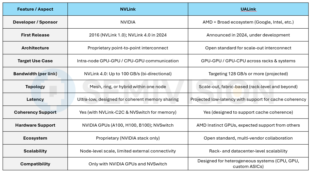
In printed circuit boards, the characteristics of copper-clad laminate (CCL) materials—including copper surface roughness, resin loss, and glass-fiber weave orientation—directly affect signal integrity (SI). Meanwhile, improper power distribution can introduce power integrity (PI) issues that in turn interfere with SI.
This article consolidates fundamental concepts and the latest industry insights, exploring the relationship between CCL material properties and high-speed SerDes channel design, while also examining how companies such asMarvell, Broadcom, and MediaTekare positioning themselves in the domains of high-speed interconnects and integrated voltage regulators (IVR).
Fundamentals of Power Integrity and Signal Integrity
In high-speed SerDes systems, the primary goal of thepower delivery network (PDN)is to provide stable power, ensuring thatsignal integrity (SI)can be maintained. If the PDN exhibits excessive impedance under transient high-current demand, the supply voltage may droop or ripple, which can disturb clock recovery, data sampling points, and eye diagrams—ultimately leading to SerDes jitter or bit errors.
In reality, capacitors arenon-ideal components, containingequivalent series resistance (ESR)andequivalent series inductance (ESL). When modeled as a series RLC element, the impedance curve exhibits aV-shaped profile: the impedance is minimized at the resonant frequency, but beyond this point, ESL dominates, and the impedance becomes inductive. PI analysis often leverages this RLC model to sweep capacitance values and ESR/ESL tolerances, evaluating whether the PDN impedance remains below the design target.
Target Impedance and AC Transient Control
Because thedynamic current waveformof modern chips is difficult to obtain, PI engineers commonly use thetarget impedanceconcept to simplify analysis:
Ztarget≈ΔVΔI
Here,ΔVis the allowable voltage variation, andΔIis the peak transient current. To ensure that supply voltage remains stable under highdi/dtload transitions, thePDN impedance across frequencymust remain below this target impedance.
A wide low-impedance band can be achieved by:
Choosingdecoupling capacitorsof different values and types
Controllingpower-to-ground plane spacingto reduce loop inductance
Minimizingparasitic inductancein the PDN path
This design approach helps suppress AC voltage droop and maintain SerDes signal integrity at multi-100 Gbps speeds.
PCB CCL Materials and Channel Loss
Copper-clad laminates (CCLs) consist offour primary components: resin, filler, glass fiber fabric, and copper foil. Theresinprovides bonding and insulation,fillersimprove thermal properties,copper foilcarries the high-speed signals, andglass fabricsupplies mechanical strength while affecting the dielectric constant.
For high-speed SerDes,low dielectric constant (Dk)andlow dissipation factor (Df)are critical to minimize channel loss. As data centers evolve from10 Gbpstoward224 Gbpsand even1.6 Tbpslinks, laminate materials are classified by loss performance into LL, VLL, SLL, ULL, and ELL grades:
LL (Low Loss): Df ≈ 0.010–0.007, suitable for <10 Gbps
ELL (Extreme Low Loss): Df < 0.002, required for 224 Gbps and 1.6 Tbps interconnects
To further reduce loss,high‑frequency‑optimized low‑profile copper foils (HVLP)are used. Copper roughness, typically characterized byRa (average roughness)andRz (peak‑to‑valley difference), directly affects conductor loss. TheHuray modelindicates that lower surface roughness results in reduced conductor loss and significantly improves high‑frequency insertion loss.

Thearrangement of glass fabricalso impacts Dk and Df.
First‑generation low‑Dk glass fabricscombined with SLL‑grade resin can achieve ~0.7 dB/in insertion loss at 13.28 GHz, supporting400G NRZchannels.
Second‑generation low‑Dk fabricswere developed for112G PAM4 and 224G PAM4, achieving ~0.85 dB/in at 26.56 GHz, suitable for1.6 Tbps switches and optical modules.
To push performance further, some vendors are developingquartz fabrics (Low‑Dk 3)that offer even lower Df and a more stablecoefficient of thermal expansion (CTE). However,supply chain and certification challengesmean that large‑scale production is not expected until2026–2027.
PAM4 and PCIe Gen6 Channel Loss
PCIe Gen6 increases the per‑lane data rate to64 Gbps. If the interface continued to useNRZ (Non‑Return to Zero)signaling, the required channel bandwidth would be around32 GHz, resulting in approximately62 dB of insertion loss—far beyond what practical equalization could handle. By adoptingPAM4 (4‑level Pulse Amplitude Modulation), where each symbol carries two bits, theeffective Nyquist frequency is halvedto roughly14 GHz, and thechannel insertion loss drops to ~33 dB, making equalization and error correction feasible.
PCIe Gen6 specifies a32 dB channel loss budget, tighter thanGen5’s 36 dB, which drives the need forULL2‑grade CCL materialsand improved PCB trace design. However,PAM4 signalingintroduces its own challenges:
The eye diagram hasthree eyes, and each eye’s amplitude isonly one‑third of NRZ, reducing SNR.
Greater sensitivity tocrosstalk, jitter, and power supply noise.
To ensure channel stability, designers must employ:
Low‑roughness copper foilsand preciseimpedance control
Enhanced decouplingand robustpower integrity design
Forward Error Correction (FEC)and advancedequalization techniques
Additionally,PAM4 testing and link adaptationrequire higher‑end instrumentation and more sophisticated algorithms. Power consumption also rises due to FEC overhead and the complexity of the equalizers.
Enterprise Strategies in High‑Speed Connectivity: Broadcom, Marvell, and MediaTek

In the era of AI‑driven data centers and ultra‑high‑speed networking, three semiconductor leaders—Broadcom, Marvell, and MediaTek—are shaping the future of high‑speed interconnects through distinct strategies.
Broadcomcontinues to dominate the switch and optical interconnect market with itsTomahawk 6—the world’s first 102.4 Tbps Ethernet switch—built on224 G SerDesand optimized for bothlong‑reach copperandCo‑Packaged Optics (CPO). Coupled with itsSian3 and Sian2M PAM4 DSPsfabricated in 3 nm, Broadcom enables 800 G and 1.6 T optical modules with ultra‑low power, targeting next‑generation data center switching and AI cluster interconnects.
Marvellpositions itself at the convergence of compute and interconnect by combining224 G SerDeswithPower‑Integrated Voltage Regulators (PIVR), which reduce PDN losses and enhance signal integrity in high‑density AI systems. Its custom silicon strategy and optical DSP portfolio strengthen its presence in hyperscale data centers and cloud infrastructure.
MediaTekhas entered the data center space withsilicon‑ready 224 G SerDes, targeting massive bandwidth for AI accelerators and cloud ASICs. ItsNVLink Fusioncollaboration withNVIDIAintegrates MediaTek’s high‑speed SerDes, optical/high‑speed I/O, inter‑chip links, and memory IP to enable heterogeneous systems, with production starting in 2026. This approach positions MediaTek as a competitive challenger to Broadcom and Marvell in scale‑up AI interconnects.
Together, these companies illustrate howsilicon leadership, SerDes innovation, CPO integration, and power‑aware system designare defining the competitive landscape for next‑generation AI and HPC connectivity.
Industry Update: Marvell

In 2025 at OFC,Marvelldemonstrated the firstPCIe Gen6 electro‑optical hybrid transmission, leveraging itsAlaska P Gen6 retimerandGen7 SerDes IPto successfully transmit PCIe Gen6 data over10 m optical fiberwith low latency and low BER in collaboration with optical module partners. Marvell also showcased400 G/lane (224 Gbaud) PAM4electro‑optical link technology, working with partners such asCoherent, Lumentum, and TeraHopto deliver800 G / 1.6 T optical modules, highlighting the company’s leadership in224 G SerDesand ecosystem integration.
ForAI large‑scale compute networks, Marvell introduced224 G SerDes, reconfigurable controllers, andlow‑latency switch corestailored toNVIDIA’s NVLinkopen specification, enablingscale‑up topologies with hundreds to thousands of accelerators. Marvell also unveiled itsPackage‑Integrated Voltage Regulator (PIVR)solution, which relocates voltage regulators from the motherboard into the package,shortening the power path significantly. PIVR provides:
Up to85% reduction in power delivery loss
2× higher current density
~15% lower system power consumption
60% reduction in power supply noise
This not only ensures cleaner power forhigh‑speed SerDesbut also saves PCB area, making it ideal fordata centers and AI platforms.
Advanced Packaging and Chiplet Strategy
As ASICs reach completion,advanced packaging becomes a critical determinantof performance and cost. Mainstream solutions today revolve aroundCoWoS (S/R/L variants), but the industry is moving towardCoPoS, which extends the concept topanel‑level packaging. This evolution creates new challenges forTGV (Through‑Glass Via) manufacturing.
Leading companies are actively investing inCoPoSbecause:
Losing share inCoWoSplus missing opportunities inglass substrate adoptionwould forfeit the next wave ofadvanced packaging.
Advanced packages increasingly integratesilicon photonics, offeringcomplete electro‑optical system solutions.
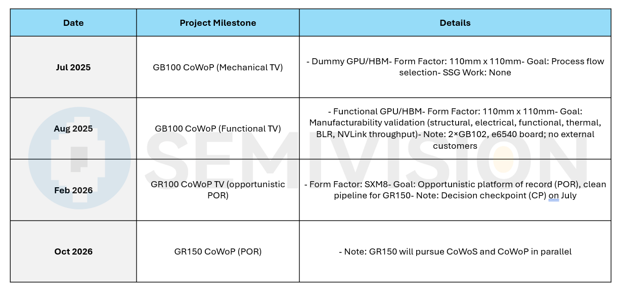

Japanese suppliers are aggressively preparing forCPO + glass substrate ecosystems, whileSamsungin Korea is also pursuing this space.TSMCis investing heavily in CoPoS, which—while conceptually related to CoWoS—differs insubstrate, scalability, and cost structure.
The semiconductor industry is at a critical inflection point. As process nodes advance to 5 nm, 3 nm, and even 2 nm, the economic and technical challenges of monolithic system‑on‑chip (SoC) designs are rising sharply. The cost of advanced processes grows exponentially, and with reticle size limits driving die area expansion, coupled with the energy surge brought by large language models (LLMs) and generative AI applications, traditional monolithic chip design is becoming increasingly unsustainable for high‑performance computing needs.
These trends are collectively pushing the industry towardchiplet‑centric, disaggregated system architectures. In this model, functionality is no longer concentrated in a single massive die; instead, it is divided into multiple specialized chiplets that cooperate within a package through high‑speed interconnects—akin to transitioning from building one giant single‑purpose factory to creating a network of smaller, specialized factories.
This architectural transition is primarily enabled by two core technologies:
2.5D integrationusing advanced interposers,
3D integrationleveraginghybrid bonding.
2.5D integrationemploys an interposer as a critical intermediary layer forpower distributionandhigh‑density chiplet‑to‑chiplet signaling, whereas3D integrationallows vertical stacking of dies to shorten interconnect distance and boost bandwidth density.
Taking 2.5D as an example, an interposer functions like an ultra‑high‑precision multilayer PCB, handling both signal routing and power delivery networks. Current mainstream solutions fall intosilicon interposersandorganic interposers:
Silicon interposersrely on back‑end semiconductor processes and fine design rules to achieve high routing density, making them suitable for extreme bandwidth requirements.
Organic interposersfeature line widths and pitches aboutfour times larger than silicon, with dielectric layers roughlytwice as thick. While their routing density is lower, they offereasier signal integrity (SI) and power integrity (PI) controlandclear cost advantages.
These material and geometric differences create cascading effects in overallpower delivery efficiency,high‑frequency loss, andcrosstalk behavior, requiring engineers to performrigorous PI and SI simulationsin the design phase. For example,organic interposersoften adoptG‑S‑G (ground‑signal‑ground)staggered routing, with adjacent layers offset to reduce vertical coupling and prevent discontinuous return paths that could cause resonances.Silicon interposers, by contrast, allowtighter shielding around tracesdue to their finer design rules and can integratedeep trench capacitors (DTCs)for enhanced decoupling, though theirpower network design is more complex.
In the engineering practice of high‑speed interconnects and chiplet packaging,224G PAM4 SerDes channel designis the clearest example of the trade‑offs involved. A 224G system is extremely sensitive to thechannel frequency response, with aNyquist frequency of 56 GHz, which imposes stringent requirements forinsertion lossandreturn losson every segment of the package path—from thechip micro‑bumps to the interposer, through thesubstrate traces, and finally to theBGA transition.
To support complex multi‑chiplet integration, engineers commonly adoptlarge multi‑core substrates, which not only improvemechanical rigiditybut also leverageinternal prepreg layers, embedded components, and fine viasto reduceparasitic parametersand enhancehigh‑frequency performance. However,long core through‑holes (PTHs)tend to introducehigh inductive behavior, degrading return loss. This requires carefulshort lateral routing,separation of PTHs from BGA transition points, andprecise time‑domain reflectometry (TDR) tuningto achieve optimal impedance matching.
Skip‑layer versus non‑skip‑layer routingeach comes with trade‑offs: the former achieves~0.13 dB/mm insertion loss, better than the latter’s~0.17 dB/mm, but with more challenging return loss performance.
Comprehensivechannel simulations and eye diagram analysesshow that bothsiliconandorganic interposers, when properly designed for 224G applications, can keeptotal channel loss below 0.5 dB, with nearly identical performance. This indicates that, in next‑generation chiplet systems,interposer selectionwill depend more onsystem size, power requirements, and overall costrather than purely on electrical performance.
Looking ahead,chiplet packaging designwill continue to balancesignal integrity (SI),power integrity (PI),package density, andmanufacturing cost, while integrating withstandards like UCIe,CPO optical interconnects, andhigh‑bandwidth memories such as HBM3e/4to support the demands ofnext‑generation high‑performance computing and AI data centers.
Therefore,future chip design, packaging, and system architecture must be conceived holistically, with all three elements considered together from the outset.
Industry Update: Broadcom
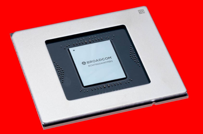
Broadcom Tomahawk Ultra
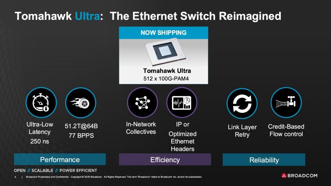
Boadcom has a new 51.2T switch chip, with a twist. Instead of going for the maximum throughput for general purpose networking, the new Broadcom Tomahawk Ultra is designed to excel at small packet sizes and low latency as a replacement for technologies like InfiniBand and NVLink with Scale Up Ethernet (SUE.)
In 2024, Broadcom launched theTomahawk 6 switch chip, the world’s first102.4 Tbps switch. It features224G SerDes lanesand supports100G/200G SerDesas well asCo-Packaged Optics (CPO), enabling long‑reach copper transmission to meet the demands of both AI‑scale deployments and traditional Ethernet networks.
In addition, Broadcom’sSian3andSian2MseriesPAM4 DSP PHYs, built on a3nm process, support200G/lane PAM4, enabling800G and 1.6T optical moduleswith low power consumption. TheSian2Mintegrates aVCSEL driver, specifically optimized for short‑reach optical links.
Together, these productssolidify Broadcom’s strong positionin the next‑generationdata center optical interconnectandCPO markets.。

Industry Update: MediaTek
MediaTek announced that its latest224G SerDeshas reached“silicon‑ready”status, delivering massive bandwidth fordata center ASICsto supportAI accelerators and cloud applications. AtComputex 2025, MediaTek andNVIDIAunveiled theNVLink Fusion collaboration, which integratesNVIDIA’s NVLink interconnect technologywith MediaTek’shigh‑speed SerDes, optical/high‑speed I/O, chip‑to‑chip interconnects, and memory IP, enablingcustomized heterogeneous systemsfor hyperscale customers.
This initiative allowsmulti‑vendor chips to operate within the same rackand is scheduled fortape‑out in 2026. The project underscores MediaTek’sactive expansion into scale‑up interconnects for data centers, positioning it tocompete with Marvell and Broadcomin the futureAI networking market.

Impact of Integrated Voltage Regulators (IVR) on SI/PI
Integrated Voltage Regulators (IVRs), orPackage IVRs (PIVRs), integrate voltage regulation functions directly within the package or near the die. This design shortens the power delivery path, reduces conductor inductance and I²·L losses, improves efficiency, and enhances transient response. For example,Marvell’s PIVR solutioncan reduce transmission loss byup to 85%whiledoubling current density.
However, IVRs generatehigh‑frequency switching noise and electromagnetic radiation, which can couple into nearby logic circuits and SerDes channels. To mitigate these effects, designers must implementadditional filtering, shielding, and layout isolation. To reduce inductor and capacitor size, IVRs typically operate athigh switching frequencies, which increasesthermal power density, requiringenhanced thermal paths in packagingoroptimized thermal interface materials (TIMs)to lower thermal resistance. As a result,PI (Power Integrity) and SI (Signal Integrity) designwith IVRs must carefullybalance efficiency, noise, and thermal management, while co‑optimizing withCCL materialsand thePDN (Power Delivery Network)to prevent regulator‑induced noise from coupling into high‑speed signal channels.
The evolution ofhigh‑speed SerDesandlarge‑scale AI networksis driving data rates from112 Gbpsto224 Gbpsand1.6 Tbps. Ensuring SI and PI requires:
UnderstandingCCL dielectric constantsandloss characteristics,
Usinglow‑roughness copper foilsandadvanced glass fiber fabricsto reduce insertion loss,
Modeling thePDN with RLC circuits, computingtarget impedance, and applyingdecoupling and loop‑inductance minimizationstrategies to suppress AC ripple and resonance.
PCIe Gen6adoptsPAM4 modulationto manage bandwidth demands, but itsstricter channel loss and noise tolerancecreate significant challenges formaterials and layout design.
In thedata center market,
Marvell, Broadcom, and MediaTekare leveraging224G SerDesandelectro‑optical integrationto capture AI networking opportunities.
Marvellfurther differentiates withPIVR technology, offeringhigh‑efficiency, low‑noise power delivery.
Broadcom’s Tomahawk 6andSian DSP seriesmaintain leadership inswitching and optical modules.
MediaTekis advancing224G SerDesandNVLink Fusionto enter thecustom AI interconnect market.
What is an Integrated Voltage Regulator (IVR)?

An Integrated Voltage Regulator (IVR) is a high-performance power management device designed to provide performance, efficiency, size, and cost benefits to energy-hungry, data-intensive, electronics applications by replacing the traditional power management integrated circuit (PMIC) solutions with a single tiny IC.
The need to provide, amongst other functions, input and output filtering, circuit protection, configurability and compensation for feedback loops means that conventional voltage regulator PMICs have to be combined with additional bulky capacitors, resistors and inductors. This is no longer the case thanks to Empower’s fully integrated voltage regulator, the first and only IVR.
The IVR is a quantum leap over traditional PMIC solutions because it combines a switching voltage regulator with all necessary control and filtering circuitry into a single packaged device, and it eliminates the need for ANY external components.


PreviousNext
TopLatestDiscussions








See all