From Glass Fiber to CCL: The Material Backbone Powering the New Era of CoWoP Packaging
From Glass Fiber to CCL: The Material Backbone Powering the New Era of CoWoP Packaging
- Source: SemiVision
- Author: SEMIVISION
- Published: 2025-07-30T22:40:57+08:00
- URL: https://tspasemiconductor.substack.com/p/from-glass-fiber-to-ccl-the-material From Glass Fiber to CCL: The Material Backbone Powering the New Era of CoWoP Packaging


From Glass Fiber to CCL: The Material Backbone Powering the New Era of CoWoP Packaging
Original Articles By SemiVision Research ( Nvidia ,TSMC ,TUC, EMC, Unimicron, Resonac, MGC, Panasonic , Nan Ya PCB)

Jul 30, 2025
∙ Paid

In the modern high-performance electronics and semiconductor packaging industry, every step of the material structure and supply chain directly determines product performance, reliability, and mass-production capability. At the most fundamental level, glass fiber combined with low dielectric constant and low-loss epoxy or PPO resin (Low Dk/Df Epoxy/PPO), laminated with copper foil, forms CCL (Copper Clad Laminate). CCL is a core material for the electronics industry, providing the essential base layer for high-frequency and high-speed circuits, and is dominated by suppliers such as TUC, EMC, Unimicron, Resonac, MGC, and Panasonic.
In advanced packaging processes, CCL serves as the core layer, which is then built up with ABF (Ajinomoto Build-up Film) and fine-pitch processing to create advanced package substrates. These substrates act as the critical bridge between chip modules and the system, enabling signal fan-out, power distribution, and mechanical support. They are indispensable for modern high-performance processors, GPUs, and AI accelerators.
However, as chip sizes grow, HBM stack layers increase, and signal rates push toward 112G / 224G SerDes, package substrates face severe challenges in warpage and thermo-mechanical mismatch in large-area, multi-layer designs. This is especially critical in ultra-large packaging solutions like CoWoS (Chip-on-Wafer-on-Substrate), where the thermal expansion and structural stability of the substrate become key limiting factors for yield and manufacturability.
From materials to packaging structure—glass fiber, resin, copper foil, CCL, ABF, and finally the substrate—every layer forms the foundation for high-performance computing and AI systems. How to continually control warpage and signal/power loss in this era of high speed, high frequency, and high power consumption is the central challenge driving future innovation in advanced packaging and material engineering.
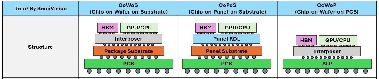
One of the hottest topics in Taiwan’s technology and semiconductor industry recently is the appearance ofCoWoP(Chip-on-Wafer-on-PCB) in NVIDIA’s latest technology roadmap. The industry already has a deep understanding ofCoWoS(Chip-on-Wafer-on-Substrate), which is the primary packaging technology for top-tier AI accelerators such as the H100 and H200. AsCoPoS(Chip-on-Panel-on-Substrate) panel-level packaging concepts begin to take shape, the next step is to further simplify the packaging hierarchy by replacing the “on Substrate” portion of CoWoS with a direct connection to the PCB, which has led to the emergence of the bold CoWoP concept.
The essence of CoWoP is to eliminate the traditional ABF package substrate and allow the chip and silicon interposer module to mount directly onto a high-precision PCB (typically an SLP, or Substrate-Like PCB), creating a direct link from the chip level to the system board. This design theoretically brings several advantages:
Shorter signal paths and lower insertion loss, which are critical for high-speed interconnects such as NVLink, PCIe Gen6/7, and HBM3/4.
Greater flexibility in thermal and mechanical design, as the bare die is directly exposed on the PCB, making it easier to implement direct-contact cold plates or liquid cooling—highly beneficial for kilowatt-class AI GPUs.
However, from a technical feasibility perspective, CoWoP presents far greater challenges than current CoWoS or CoPoS approaches, including:
PCB precision requirements: The system board must take over the high-density routing role of the original package substrate, achieving line width/spacing of 15–20 μm or less, while maintaining strict flatness and dimensional stability.
Thermo-mechanical reliability: With bare dies and interposers directly mounted on the PCB, thermal cycling and CTE (coefficient of thermal expansion) mismatch can cause solder fatigue and amplified warpage risks.
According to discussions with Taiwanese PCB and packaging manufacturers, proof-of-concept samples have indeed been submitted for testing, indicating that NVIDIA’s CoWoP approach is not just theoretical but is undergoing early-stage technical validation. However, the industry consensus is that CoWoP willnotbe used for mass production in the NVIDIA Rubin Ultra generation, and NVIDIA is more likely to continue with a mix of CoWoS and CoPoS solutions to ensure product reliability and supply stability.
CoWoP represents a potential future direction for system-level packaging, but due to challenges in manufacturing precision, cleanroom requirements, and yield control, the Rubin Ultra generation will still primarily rely on CoWoS. True commercialization of CoWoP may require at least one to two more product generations before it can reshape the packaging models and supply chain ecosystem for HPC and AI servers.
It can therefore be concluded that the core concept of CoWoP is to replace the traditional CoWoS structure, where the silicon interposer rests on a package substrate and PCB, with a single ultra-thin SLP (Substrate-Like PCB)that serves both functions.
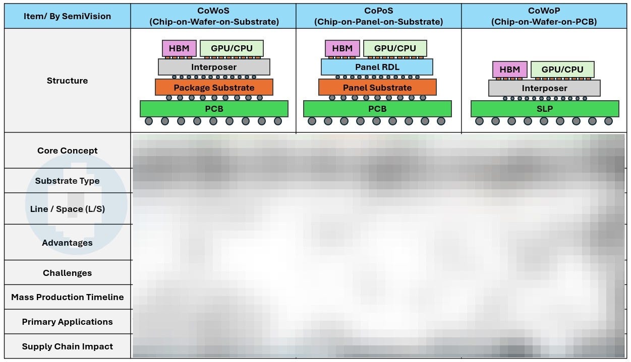
For Paid Members ,SemiVision will discuss topics on
Origin and Technical Analysis of CoWoP
PCB Manufacturing Methods and SLP/MSAP
mSAP and Optical Modules as Early Catalysts
HVLP (High-Frequency Very Low Profile) Copper Foil and Ultra-Thin Copper Foil Market Analysis
Shin‑Etsu Chemical Develops Innovative Equipment and Methods for Advanced Packaging Substrates
AI Accelerators Driving Demand for CCL and PCB
What is Glass Fabric?
Electronic-Grade Glass Fiber Fabric for Special Composite Materials
Glass fiber manufacturing
Electronic fabric is a key reinforcement material for copper-clad laminates (CCL).
Key Technical Parameters of Electronic Fabric: Dielectric Constant & Dielectric Loss
Why Does Signal Transmission Through Copper Get Affected by the Dielectric Constant / Dielectric Loss of Electronic Fabric?
Impact of Electronic Fabric on Copper Clad Laminate (CCL) Parameters
Specialty Electronic Glass Fabrics: Essential for AI Hardware, Devices, and Chip Packaging
224G High-Speed Interconnect Solutions Enter Research Stage
Development Highlights of Second-Generation Ultra-Low Df Quartz Electronic Fabric
Origin and Technical Analysis of CoWoP
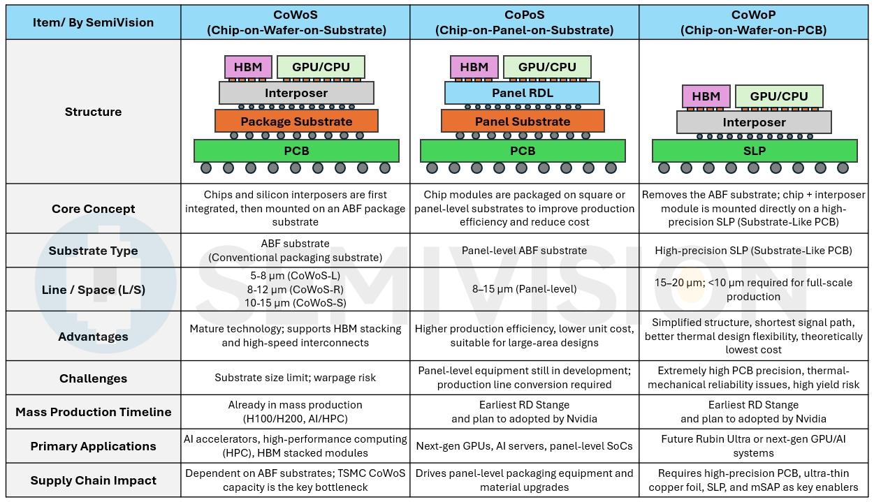
CoWoS, CoPoS, and CoWoP represent different stages in the evolution of advanced packaging technologies, each with distinct structures and applications.CoWoS(Chip-on-Wafer-on-Substrate) is currently the primary packaging solution for high-end AI accelerators such as NVIDIA’s products . Its core concept involves first integrating the GPU/CPU and HBM on a silicon interposer, which is then mounted on an ABF (Ajinomoto Build-up Film) package substrate. It supports line widths and spacing of 5–8 µm for CoWoS-L and up to 10–15 µm for CoWoS-S, offering mature technology and high-frequency, high-speed interconnect capability, but it is constrained by substrate size and warpage risks.
CoPoS(Chip-on-Panel-on-Substrate) further introduces panel-level ABF substrates with redistribution layer (RDL) structures, enabling packaging on square or large-area panels to improve production efficiency and reduce cost. Its line width/spacing is around 8–15 µm, suitable for large-area designs, though it requires new equipment and production line conversions. CoPoS is currently in the R&D and early adoption phase, targeting next-generation GPUs and AI server applications.
CoWoP(Chip-on-Wafer-on-PCB) is the most aggressive approach, completely removing the ABF substrate and directly mounting the chip-and-interposer module onto a high-precision PCB, such as an SLP (Substrate-Like PCB). Theoretically, this achieves the shortest signal path, improved thermal management flexibility, and the lowest cost. However, it demands PCB precision of 15–20 µm and even below 10 µm for full-scale deployment, and it faces significant thermo-mechanical reliability and yield challenges. Currently, it remains at the proof-of-concept stage, with potential applications in the Rubin Ultra platform or future high-power GPU/AI systems.
In summary, these three approaches correspond to different stages: CoWoS for mature mass production, CoPoS as a panel-level transitional solution, and CoWoP as a system-level innovation. Each imposes different material and technical requirements across the supply chain, including ABF substrates, high-precision PCBs, ultra-thin copper foils, and mSAP (Modified Semi-Additive Process) manufacturing technology.
NVIDIA’s latest technology roadmap introduces the concept of CoWoP (Chip-on-Wafer-on-PCB). The industry already has a deep understanding of CoWoS (Chip-on-Wafer-on-Substrate), which is currently the main packaging technology for top-tier AI accelerators such as the H100 and H200. As CoPoS (Chip-on-Package-on-Substrate)panel-level packaging concepts gradually take shape, the next step is to further simplify the packaging hierarchy—replacing the “on Substrate” stage of CoWoS with a direct implementation on the PCB—leading to the emergence of the bold CoWoP approach.
The essence of CoWoP is to remove the traditional ABF package substrate and mount the chip and silicon interposer module directly on a high-precision PCB (typically an SLP, or Substrate-Like PCB), forming a direct connection from chip level to system board level. This design theoretically offers several key advantages:
Shorter signal paths and lower insertion loss, which are critical for high-speed interconnects such as NVLink, PCIe Gen6/7, and HBM3/4.
Greater thermal and mechanical flexibility, as bare dies are directly exposed on the PCB, making it easier to implement direct-contact cold plates or liquid cooling—particularly advantageous for kilowatt-class AI GPUs.
However, the technical challenges of CoWoP are significantly higher than those of existing CoWoS or CoPoS solutions, including:
PCB precision requirements: The system board must take over the high-density routing functions of the package substrate. Line width/spacing (L/S) must reach15–20 μm or below, while maintaining strict flatness and dimensional stability.
Thermo-mechanical reliability: Bare dies and interposers mounted directly on the PCB face amplified solder fatigue and warpage risks due to thermal cycling and coefficient of thermal expansion (CTE) mismatches.
Discussions with Taiwanese PCB and packaging manufacturers confirm that proof-of-concept samples have been submitted for testing, showing that NVIDIA’s CoWoP path is not merely theoretical but is under early technical evaluation. However, industry consensus indicates that CoWoP will not be adopted for mass production in the NVIDIA Rubin Ultra generation, with the company likely continuing to rely on a hybrid of CoWoS and CoPoS to ensure product reliability and supply stability.
According to research from Japanese supplier Ibiden, the ABF substrate area of Rubin Ultra is significantly larger and has more layers than Rubin, making a transition to CoWoP extremely challenging. To adopt CoWoP, PCB L/S would need to shrink below 10/10 μm to match the current ABF substrate level. In comparison, the average L/S of HDI boards is 40/50 μm, and iPhone mainboards using SLP (Substrate-Like PCB) achieve about 20/35 μm.
In the long-term outlook, CoWoP could simplify GPU board manufacturing. If adopted, it is expected to rely on mSAP (Modified Semi-Additive Process) technology, similar to that used in SLP. The likely beneficiaries would include Taiwanese PCB makers such as Zhen Ding, Compeq, and Unimicron, as well as international suppliers like AT&S and TTM. However, for ABF substrate suppliers, the adoption of CoWoP would likely have negative implications.
CoWoP (Chip-on-Wafer-on-PCB) Origin and Technical Analysis
CoWoP (Chip-on-Wafer-on-PCB) has recently become a widely discussed topic in advanced packaging. Its core concept is toremove the traditional package substratein CoWoS (Chip-on-Wafer-on-Substrate) and directly mount the chip module with an organic interposer onto areinforced PCB, aiming to shorten signal paths, improve thermal performance, and mitigate warpage in large-scale packages. This idea is not entirely new, as a similarCoB (Chip-on-Board)process is already widely used in consumer electronics and automotive semiconductors. However, applying this concept to high-performance AI accelerators and GPU platforms is a highly challenging system-level innovation.
PCB Manufacturing Methods and SLP/MSAP
SLP (Substrate-Like PCB) usesMSAP (Modified Semi-Additive Process)to achieve finer line width/spacing compared to the traditional subtractive etching method.
- Subtractive Process (Etching Method)
Uses thick copper foil covering the entire panel, then defines circuits via photoresist, exposure, and etching.
Limited by etching precision and prone to edge roughness.
- Additive Process
Starts with an insulating base and selectively plates or deposits copper only where needed.
Can achieve extremely fine lines but has higher cost and lower mass-production efficiency.
- Semi-Additive Process (SAP / MSAP)
Begins with a thin copper base, defines the pattern, plates up the traces, and etches away unwanted base copper.
Can achieve~10 μm L/Swith better production efficiency than full additive processes.
Industry Status and Challenges
Current Applications: SLP is currently used inNVIDIA’s 800G and 1.6T optical modules, where small form factors and controlled warpage make it feasible.
GPU Board Adoption: Large GPU boards face significant warpage risks, so CoWoP requires long-term qualification.
Supply Bottleneck: The key bottleneck for CoWoP isultra-thin copper foil, not the SLP itself. This material is critical for scaling up production.
From an application and timeline perspective, CoWoP is unlikely to enter mass production in AI accelerators or GPUs in the near term. It is expected to remain non-mainstream until at least 2028. While NVIDIA has included CoWoP in its internal roadmap for the Rubin Ultra platform to address thermal and warpage challenges, mass production will still rely on CoPoS (Chip-on-Package-on-Substrate) or other mature transitional solutions. CoPoS uses a process similar to CoWoS but adopts square panel-level packaging to improve throughput, with the required equipment not expected to be ready until the end of 2026.
mSAP and Optical Modules as Early Catalysts

In the meantime, the primary driver for mSAP adoption will come from high-speed optical modules. 1.6T silicon photonic transceivers are extremely sensitive to signal density and insertion loss, and SLP—achieving <20 μm L/S—has a clear advantage over traditional HDI boards with 40–45 μm L/S.
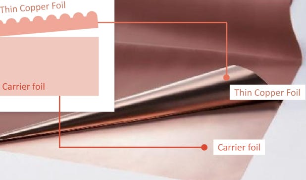
Upstream, Mitsui Mining dominates the supply of 1.5 μm ultra-thin electrolytic copper foil, which is critical for SLP and CoWoP. As optical modules ramp up and future GPU platforms gradually adopt CoWoP, mSAP technology and high-precision PCB will become essential enablers for advanced packaging and system integration, driving a new wave of value creation across the PCB, packaging, and materials supply chains.
HVLP (High-Frequency Very Low Profile) Copper Foil and Ultra-Thin Copper Foil Market Analysis
In high-speed signal transmission design, the concept of “Lower Df / Dk BUF” highlights that for 56G, 112G, and even 224G PAM4 SerDes and AI/HPC systems, selecting PCB materials with low dissipation factor (Df) and low dielectric constant (Dk) is essential to reduce channel loss and maintain signal integrity (SI). The primary sources of high-speed transmission loss are dielectric loss and conductor loss, so the characteristics of the substrate materials directly determine whether data can be reliably transmitted at extremely high frequencies.
First is Df (Dissipation Factor), which represents dielectric loss. A lower Df means the material dissipates less energy internally, allowing electromagnetic energy to propagate with slower attenuation along the PCB transmission line. For long-reach 56G/112G/224G PAM4 signaling, Df often dictates whether the system can achieve the target BER. Second is Dk (Dielectric Constant), which defines how much electric field energy a material can store per unit length. A lower Dk translates to faster charging and discharging of transmission lines, reduced latency and jitter, and better impedance stability—critical for ultra-high-speed channels in the 28 GHz to 100 GHz range. The third key factor is copper surface roughness R(f), which directly affects conductor loss. At higher frequencies, the skin effect causes current to concentrate near the conductor surface, and a rougher copper surface forces current to meander, increasing scattering and resistive loss. Therefore, designs targeting 56G/112G often require ultra-low-profile copper foils like HVLP4 to HVLP5 to mitigate high-frequency conductor loss.

The physical behavior of high-speed channel loss can be described using simplified formulas. Conductor loss (αc) is proportional to the square root of the dielectric constant and the copper surface roughness, expressed as αc ∝ √Dk × R(f). Dielectric loss (αd) is proportional to the signal frequency and the square root of Dk × Df, expressed as αd ∝ 27.3 × f / c × √(Dk × Df), where c is the speed of light. This means that at higher frequencies, the importance of Df and copper surface properties is amplified, as these two factors dominate high-frequency loss. The yellow cross-section diagram of copper foil in the slide visually demonstrates how surface roughness impacts conductor loss: the smoother the surface, the lower the skin-effect-induced attenuation. In next-generation 1.6T and 3.2T switch applications, HVLP-grade copper foil is essentially mandatory.

Overall, the design targets are explicit: Df ≤ 0.005 to minimize signal loss, Dk ≤ 3.3 to ensure impedance stability and low latency, and copper surface roughness (Ra/Rz) should be minimized—typically evaluated using low-Ra foils and simulated accurately with the Huray model. This material and design strategy directly aligns with the needs of 224G PAM4, 1.6T/3.2T switches, and CXL 3.0/4.0 as well as AI/HPC high-speed interconnects. It represents the integration of physical modeling and real-world industry practices, serving as the core guideline for controlling channel loss in next-generation ultra-high-speed PCB design.
In high-speed PCB design, material parameter selection is critical to signal integrity. The recommended design targets are: Dissipation Factor (Df) ≤ 0.005 to minimize dielectric loss and reduce signal attenuation; Dielectric Constant (Dk) ≤ 3.3 to ensure impedance stability and lower transmission delay; and copper surface roughness with as low Ra as possible to reduce conductor loss and high-frequency scattering caused by the skin effect. These parameter requirements align closely with the current material selection trends for high-speed PCBs, pointing toward Ultra-Low Loss (ULL) and even Extreme Low Loss (ELL) laminates to meet the stringent channel loss requirements for 56G, 112G, and 224G PAM4 links as well as AI/HPC high-speed interconnects.
- Overview of HVLP Copper Foil
HVLP (High-Frequency Very Low Profile) copper foil is a specialized electronic material designed forhigh-frequency, high-speed signal transmission. Its core characteristics includeextremely low surface roughness, minimal signal loss, high peel strength, and excellent thermal stability. The surface roughness (Rz) typically ranges from0.8 to 1.5 μm, effectively reducing high-frequency losses caused by theskin effect, while maintaining uniform thicknesses of12–70 μm, meeting the stringent requirements of advanced PCB and substrate manufacturing.
Key applications includeAI accelerators, 5G communication devices, high-speed servers, router backplanes, and optical network modules.
- Performance Advantages
Low insertion loss at high frequencies (10–40 GHz): Critical for112G/224G SerDes, high-speed CPO/LPO optical modules, and future AI/HPC platforms.
Excellent thermal reliability: Advanced H1A and V1A grades can withstandup to 295 °C, maintaining dimensional stability and ductility under prolonged high-temperature operation or multiple thermal cycles.
Micro-nodular copper surface design: Using micro-spherical or fibrous nodules withnon-uniform distributionreduces surface roughness while ensuring strong adhesion to dielectric layers, further improving signal integrity and reducing high-frequency loss.
- Manufacturing and Structure
HVLP copper foil is produced viaelectrolytic base foil processing. During drum electroplating, asmooth shiny sideand amatte sideare formed. The matte side undergoesmulti-layer surface treatments:
Microstructure roughening layer
Coupling agent layer
Anti-oxidation and barrier layers
This structure achieveslow roughness with sufficient peel strength, ensuring compatibility with high-speed PCB manufacturing and long-term reliability.
- Application Fields
AI accelerators and high-end servers:
High-frequency substrates for HBM + GPU modules
Support forCXL, PCIe Gen6/Gen7high-speed interconnects
5G communication equipment:
Millimeter-wave antenna boards, RF front-end modules
5G macro base stations and optical network devices
Data centers and networking:
800G/1.6T switches and router backplanes
CPO, LPO, and NPO optical modules requiring high-speed signal transmission
- Industry Landscape and Supply Chain
The high-end HVLP copper foil market remainsdominated by Japanese and Taiwanese manufacturers:
Japan: Mitsui Mining, JX Nippon, Fukuda
Taiwan: Nan Ya PCB Materials
China: Jin’an Guoji, Chaohua, and Nord, mostly focused on mid-to-low-end products
Since HVLP copper foil is akey enabler for 5G, AI/HPC, and high-speed optical equipment, supply capability directly impacts mass production schedules of servers and optical modules. With the ramp-up of224G SerDes, large-scale CPO modules, and next-generation HPC platforms, the HVLP market is entering ahigh-growth phase.
- Technology Roadmap

The red line indicates the 2 µm roughness threshold, which is commonly regarded as the upper limit of surface roughness tolerance for advanced packaging processes such as RDL or hybrid bonding.
Future development focuses onlower roughness, better signal integrity, and enhanced dimensional stability. The industry is progressing fromHVLP2 → HVLP3 → HVLP4 → profile-freecopper foils to support next-generation high-speed interconnects and higher power density designs. Key growth drivers include:
5G millimeter-wave and optical modules (CPO/LPO)
AI/HPC SLP-based substrates (e.g., NVIDIA Rubin Ultra)
- Ultra-Thin Copper Foil (1.5 μm) and Mitsui Mining’s Market Position
Mitsui Mining’s electronic materials business is amajor growth driver, especially inultra-thin electrolytic copper foil and HVLP copper foil. The1.5 μm ultra-thin copper foilwas initially developed forSLP (Substrate-Like PCB)in smartphones, enablingMSAP (Modified Semi-Additive Process)for ultra-fine line patterns, such as10/10 μm L/Sin iPhone A-series application processors.
2018–2022: Smartphone SLP demand peaked
Post-2022: Growth stagnated due to a lack of new demand drivers
New market dynamics since 2024:
800G & 1.6T optical modules:
Adopt SLP to reduce size, improve signal integrity, and minimize insertion loss
While per-unit copper consumption is lower than smartphones, the rapid CPO/LPO adoption makes demand substantial
Future CoWoP GPU platforms:
If implemented, server motherboards will require high-precision SLP with1.5 μm ultra-thin copper foil, significantly increasing demand
Supply chain concentration:
Mitsui Mining holds~100% market sharein stable 1.5 μm production
Fukuda and JX Nippon produce limited ultra-thin foils
China hasnot yet commercialized <3 μm foils, still focused on5–12 μmproducts for consumer electronics and Li-ion batteries
- Market Outlook
The demand growth trajectory is clear:
iPhone → 800G/1.6T Optical Modules → NVIDIA Rubin Ultra (It has potential but is challenging).
Mitsui Mining willdirectly benefitfrom this trend but will also facecapacity expansion, yield control, and delivery challenges. As optical modules scale and future GPU platforms adopt CoWoP,mSAP-based high-precision PCB and ultra-thin copper foilwill become the backbone of advanced packaging and system integration, driving anew wave of value creation across the PCB, packaging, and materials ecosystem.。
Shin‑Etsu Chemical Develops Innovative Equipment and Methods for Advanced Packaging Substrates
Shin‑Etsu Chemical recently announced the development of aninnovative piece of equipment and manufacturing methoddesigned for advanced packaging substrates, aiming to enhance production capabilities for next-generation chiplet and high-frequency, high-speed packaging. This new system introduces thedual damasceneprocess—commonly used in front-end semiconductor fabrication—into back-end substrate manufacturing, combined withhigh-precision excimer lasertechnology. The process enables the direct formation offine wiring and via structureson multilayer organic insulating materials. By doing so, the substrate itself can perform the functions of a traditionalsilicon interposer, eliminating the need for a separate interposer layer and its associated process steps, thus effectivelyreducing overall manufacturing cost and capital expenditure.
Compared with the traditionalSAP (Semi-Additive Process)method, Shin‑Etsu’s new processexceeds the miniaturization limitsof dry-film photoresist techniques, enablingfiner wiring structuresideally suited for chiplets, multi-die integration, and high-performance computing platforms demandingextreme signal integrity. This approach not onlyenhances design flexibilitybut alsosupports the stringent requirements of future high-frequency, high-speed, and high-power advanced packaging.
In addition, Shin‑Etsu is pursuing anintegrated materials-and-equipment strategy, providingend-to-end solutionsfrom material development to equipment manufacturing. This integration is expected toaccelerate the adoption of chiplet packaging technologiesand optimize theprocess efficiency and cost structureof the overall packaging ecosystem. Bybypassing the traditional interposerand supporting2 µm trench / 5 µm via-level fine wiring, this technology is set to become akey enabler for next-generation high-frequency, high-speed packaging and chip modularization.
As we mentioned earlier, the computing power of AI chips continues to grow, with rapidly increasing core power consumption and bandwidth requirements, placingstricter demands on PI (Power Integrity)andSI (Signal Integrity). When chips reach kilowatt-level power and adopt112G/224G SerDesorHBM3/4 high-speed interfaces, any power noise or signal loss can directly impact system performance and stability.
AI Accelerators Driving Demand for CCL and PCB
With the rapid expansion of AI accelerators and data center computing needs, the demand forhigh-end CCL (Copper Clad Laminate)andPCB (Printed Circuit Board)materials across the supply chain is rising sharply. This trend not only elevates the specifications of materials being adopted but also reshapes the competitive landscape and business opportunities for related suppliers.
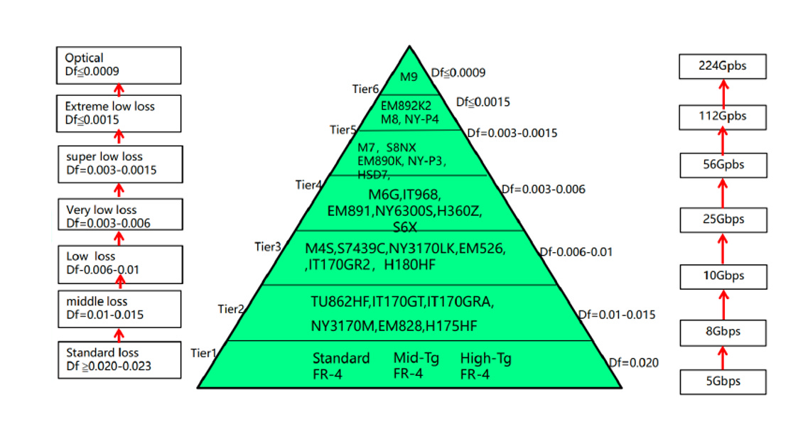
Currently, most AI servers still utilizeM7-grade CCL materials, but as computing density and bandwidth requirements continue to grow, the industry is rapidly transitioning towardM8 and even M9-grade materials. AWS is among the first cloud providers to adoptM8-grade CCL, with its T2 platform already incorporating higher-spec materials. According to industry data, a single NVIDIA GPU currently consumes about$100 worth of CCL materials, while the latest AWS GPU generation is estimated to require$400–500 in CCL materials per GPU, reflecting a remarkable increase in cost.
NVIDIA’snext-generation Rubin platformand Google’schip(developed by MediaTek) are expected to adoptM9-grade CCL. If deployed with theCordeliapackage, material costs may be slightly lower than theBiancaarchitecture. Within the M9 class, there are further distinctions: for example,Taiwan Union Technology (TUC)categorizes products into896K2(sometimes referred to as M8.5) and896K3. In 2025,896K2will remain the mainstream product, while896K3will mainly serve high-endKyber backplanes, with unit prices reachingaround NT$30,000 per sheet(actual purchase prices are slightly lower but still significantly higher than current M7 or M8 products). Notably,896K2is roughlytwice the price of existing materials, underscoring how heavily AI computing platforms now rely on advanced material performance.
In summary, thematerial evolution pathfor AI chip platforms is clear:M6 → M7 → M8 → M9. This transition directly benefitsCCL suppliers(such asTUC and Panasonic),PCB manufacturers(such asTTM), andupstream copper foil and glass fiber suppliers. As896K2 and 896K3enter mass production in mainstream platforms,ASP (average selling price)anddemand volumefor CCL/PCB are both entering a high-growth phase, making these materials astrategically critical part of the AI hardware supply chain.
As we gain a clearer understanding ofelectronic-grade glass fiber fabricand its critical role incopper-clad laminates (CCL), it becomes evident that this material is not only the structural backbone of PCBs but also a key factor in ensuringsignal integrity (SI)andpower integrity (PI)at high speeds. From the development oflow-Dk/Df materialsto the adoption oflow-CTE and quartz fibers, these advancements directly address the demands of next-generation high-performance computing, AI servers, and224G high-speed interconnects.
Next, we will transition from the fundamental properties and manufacturing processes of these materials to theirreal-world applications, illustrating how glass fiber fabrics and CCLs underpin the design and mass production ofnext-generation AI chips, data center servers, and high-frequency, high-speed networking equipment.
What is Glass Fabric?

Glass fiber fabric (also known as glass cloth or fiberglass fabric) is a woven material made from glass fiber yarns. It is known for its high tensile strength, excellent thermal and chemical resistance, non-flammability, superior electrical insulation, and dimensional stability. These characteristics make it a critical reinforcement material in various industrial and electronic applications.
Electronic-grade glass fiber fabric is woven from specially specified glass fiber yarns. With its excellent mechanical strength, heat resistance, chemical durability, flame retardancy, electrical insulation, and dimensional stability, it serves as a key raw material in the production of copper-clad laminates (CCL)—the core substrates of electronic components. These properties enable the finished PCBs to meet demanding electrical and mechanical performance standards.

As a result, electronic-grade glass fiber fabric is widely used in the manufacturing of smartphones, laptops, automotive electronics, aerospace instruments, and other high-tech electronic devices.
From an application perspective, electronic-grade glass fiber fabric is generally classified into two main categories:
Glass fabric for printed circuit boards (PCBs):
Used as the core reinforcing material in CCLs for multilayer PCBs, enabling high-performance interconnects in consumer and industrial electronics.
Glass fabric for special composite materials (non-PCB applications):
Commonly referred to in the industry as "industrial fabric", this type is used in fields requiring high-strength, high-temperature, and chemical-resistant composite structures, such as aerospace, defense, insulation, and filtration systems.
Electronic-Grade Glass Fiber Fabric for Special Composite Materials

Electronic-grade glass fiber fabric is widely used as a base and reinforcing material in a variety of high-performance composites across multiple industries, including automotive structures, electrical insulation, high-temperature thermal protection, construction, aerospace, and sporting goods. By combining with various organic or inorganic materials, it enables the production of composites with exceptional strength, durability, thermal resistance, and dimensional stability. These composites are extensively applied in industrial, architectural, transportation, and environmental protection sectors, making electronic-grade glass fabric a key material in the broader national economy.
Glass fiber manufacturing

Resin-impregnated continuous strands(woven roving,mat,or impregnated roving) are wound onto a mandrel in specific patterns and then cured to form the finished products,it includes discontinuous filament winding and continuous filament winding.
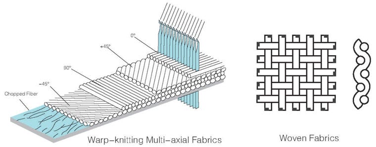
Weaving is the process of making fabrics by layer-spreading or intersecting roving reinforcements with filling yarns.
Electronic fabric is a key reinforcement material for copper-clad laminates (CCL).
Copper-clad laminate (CCL) serves as the substrate material for manufacturing printed circuit boards (PCBs). CCL is produced by impregnating reinforcement materials—such as wood pulp paper or glass fiber fabric—with resin, then laminating copper foil on the surface and applying hot pressing. The upstream materials of CCL include copper foil, resin, and glass fiber fabric.

Key Technical Parameters of Electronic Fabric: Dielectric Constant & Dielectric Loss
Dielectric Constant Dk (Dielectric Constant)
Also known as permittivity or relative permittivity (commonly denoted as εr), it represents a material’s ability to store electrical energy when subjected to an electric field. It reflects the material's influence on the electric field. A lower Dk value results in faster signal transmission within the material and reduced delay, making it more suitable for high-speed signal transmission.
Dielectric Loss
Dielectric loss refers to the energy loss phenomenon that occurs in dielectric materials when subjected to alternating electric fields, caused by internal charge displacement lagging behind the field changes. This energy loss is typically manifested as heat. It occurs during the storage and release of energy in the dielectric (polarization and depolarization), and in processes involving irreversible energy loss (such as molecular friction and charge leakage), reflecting the material’s capability to convert electrical energy into heat.
Dissipation Factor Df (Dissipation Factor)
Also known as the "loss tangent", Df is a parameter that quantifies the degree of dielectric loss in materials. It directly impacts circuit efficiency, heat generation, and signal distortion. Lower Df values correspond to reduced signal transmission loss.
Why Does Signal Transmission Through Copper Get Affected by the Dielectric Constant / Dielectric Loss of Electronic Fabric?
Signals don’t just “flow” through copper: While signals primarily travel along copper traces, the dielectric constant of the electronic fabric plays a critical role in maintaining signal integrity because of electromagnetic field propagation characteristics, which are highly dependent on the dielectric properties of the PCB material.
When a signal propagates through a transmission line, the signal forms an electromagnetic field around the conductor, which interacts with the dielectric material (typically resin-based) that acts as a "return path." As a result, the dielectric constant of the material directly influences the electromagnetic field distribution and energy loss.
An analogy: This is similar to how the characteristics of pipe materials affect flow resistance in fluid transport — in signal transmission, the εr of the dielectric material determines the "magnetic permeability," which affects the degree of energy loss in signal transmission.
Impact of Electronic Fabric on Copper Clad Laminate (CCL) Parameters
Copper Clad Laminates (CCL) typically consist of electronic fabric (such as glass fiber), resin matrix (such as epoxy or polyimide), and copper foil. Among these, electronic fabric serves as the reinforcing structure, and its dielectric properties combined with the resin matrix’s dielectric characteristics determine the overall dielectric constant (εr) and dielectric loss tangent (tan δ) of the CCL.
The dielectric constant of the CCL can be regarded as the "weighted average" of the dielectric constants of glass fiber and resin, following the mixing rule:

If the dielectric constant of glass fiber is higher than that of resin, increasing the content of glass fiber in the composite will raise the overall εr of the CCL. Conversely, if the dielectric constant of glass fiber is lower than that of resin, the overall εr will decrease.
The woven structure of glass fiber causes anisotropy in the dielectric constant of the CCL. The εr in the plane of the glass fibers (warp and weft direction) is dominated by glass fiber and tends to be higher, while the εr in the direction perpendicular to the glass fibers (thickness direction) is dominated by the resin matrix and is lower. A large disparity in the dielectric constants of glass fiber and resin will increase the anisotropy in the CCL, potentially affecting signal integrity.
➤ The dielectric loss of CCL is similarly determined by the combined losses of glass fiber and resin.
If the tan δ of the glass fiber is high, it directly increases the overall dielectric loss of the CCL, especially at high frequencies (e.g., above 10 GHz), where the signal attenuation caused by dielectric loss is more significant. Using specialized glass fibers can significantly reduce the tan δ of the CCL.

Continuous Modification of Fiberglass: Quartz Fiber Offers Superior Dielectric and Thermal Expansion Properties
According to the study“Research on Composition and Properties of Low-Expansion Alumino-Borosilicate Electronic Glass Fibers”, electronic-grade fiberglass can be classified by composition into E-glass, D-glass, NE-glass, and L-glass:
E-glassis the typical traditional electronic glass fiber, with a dielectric loss of 0.0060 at 1 MHz.
D-glassoffers better dielectric loss and a lower coefficient of thermal expansion (CTE) than E-glass, but suffers from manufacturability issues and performance defects in finished products.
NE-glassandL-glass, developed based on D-glass, also exhibit poor manufacturability despite improved properties.
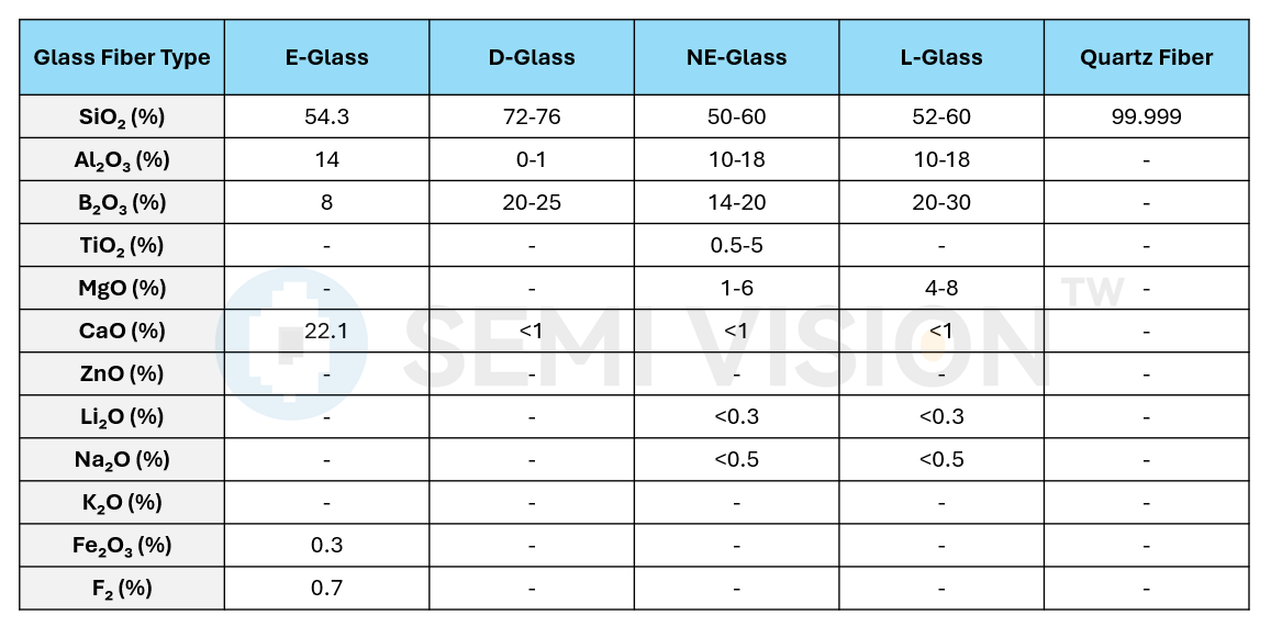
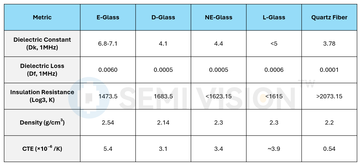
In comparison,quartz fiberoutperforms all the aforementioned glass fibers, offering the best dielectric properties and the lowest thermal expansion coefficient.
Specialty Electronic Glass Fabrics: Essential for AI Hardware, Devices, and Chip Packaging
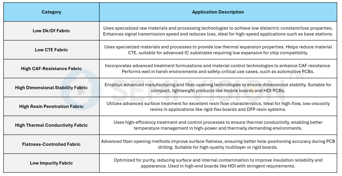
Specialty electronic glass fabrics include low-dielectric constant (Low-Dk) fiberglass cloth, low coefficient of thermal expansion (Low-CTE) fiberglass cloth, and quartz fiber fabrics.
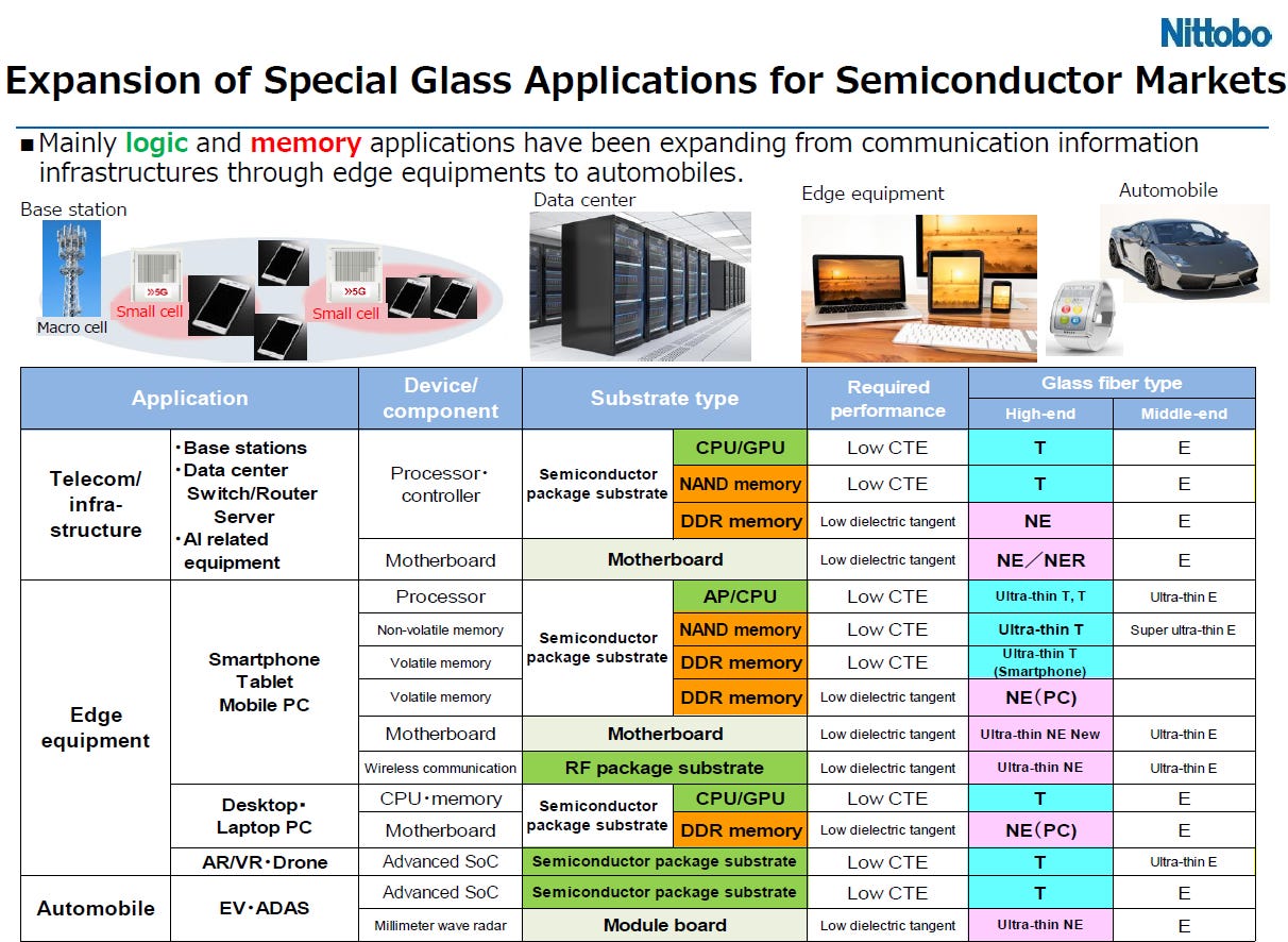
T refers to Low-CTE (Low Coefficient of Thermal Expansion) fibers.
NE refers to the first-generation Low-Dk (Low Dielectric Constant) fiberglass.
NER refers to the second-generation Low-Dk fiberglass.
According to Nittobo, in the era of computational power, both AI hardware and terminal devices demand higher-performance materials for chips. Low-Dk fiberglass cloth is primarily used for motherboard substrates, while Low-CTE fiberglass cloth is applied to chip packaging substrates. With the rapid surge in AI demand, both types of glass fabrics are now scaling up significantly. Due to their high technical and supply barriers, the market is experiencing a supply shortage.
Copper-clad laminate (CCL) accounts for 40% of the total cost of a PCB, while glass fiber fabric is the key material in CCL manufacturing, representing 18% of the material cost of CCL.
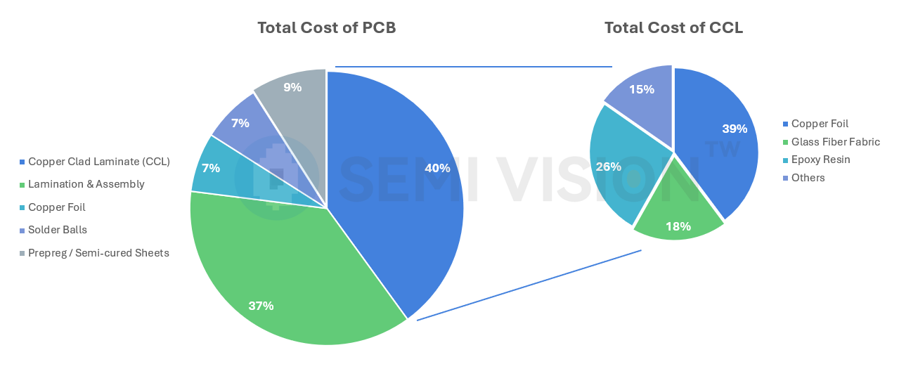
According to the Glass Fiber Technology Information channel and public market reports, the unit price of second-generation Low-DK glass fiber fabric has reached RMB 120/meter, and Low-CTE glass fiber fabric has reached RMB 130/meter. These prices represent increases of 243% and 271%, respectively, compared to first-generation Low-DK glass fiber fabric. Correspondingly, the net profit margin has improved by 3 percentage points and 5 percentage points, respectively.
224G High-Speed Interconnect Solutions Enter Research Stage
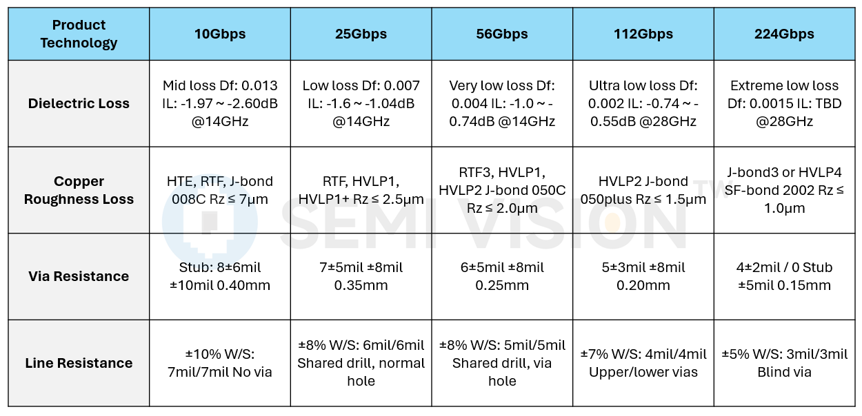
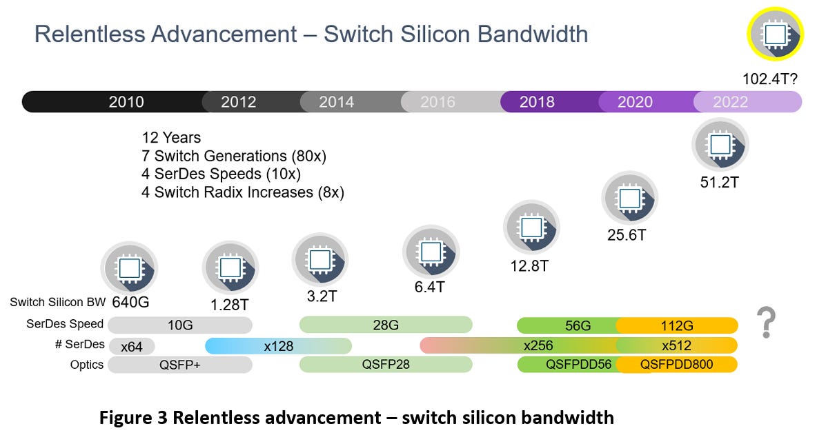
According to ZTE's whitepaper “224G High-Speed Interconnect Requirements and Challenges for PCB and Copper Clad Laminate (CCL)”, the industry has entered the pre-research phase for 224G high-speed interconnect technologies. Leading chip vendors such as Marvell, Broadcom, and NVIDIA have already launched R&D initiatives targeting this next-generation interconnect standard. The proposed solutions encompass both optical-electrical interconnects and advanced PCB and cable technologies.
At such ultra-high speeds, motherboards designed to support 224G interconnects rely primarily on high-speed PCB materials. This significantly raises performance requirements on multiple fronts:
Dielectric loss of PCB substrates: Materials must exhibit lower dielectric loss to preserve signal integrity at higher frequencies.
Copper loss: The resistivity of copper becomes a limiting factor, necessitating purer materials or novel copper processing techniques.
Conductor (trace) loss: Line geometry and surface roughness directly impact high-frequency signal attenuation.
Via loss: Signal degradation through vias (vertical interconnects) becomes more pronounced, requiring optimized via structures and potentially embedded optical solutions.
Consequently, the development of next-generation PCB substrates must be tightly coupled with advancements in PCB processing technologies, ensuring the entire signal pathway is capable of supporting 224G data rates with minimal loss and distortion.
This research stage is foundational for enabling the infrastructure required by future AI computing, data centers, and ultra-high bandwidth networking equipment, where data transmission efficiency at 224G speeds will be critical.

Material Performance Requirements for Data Centers
According to ZTE's "224G High-Speed Interconnect: PCB and CCL Demands and Challenges", data centers are one of the primary application fields for 224G technologies. Key data center hardware—servers, network routers, and storage systems—rely heavily on high-speed PCBs. For instance, servers mainly utilize four major categories of PCBs.


Market Potential and Competitive Landscape of CCL
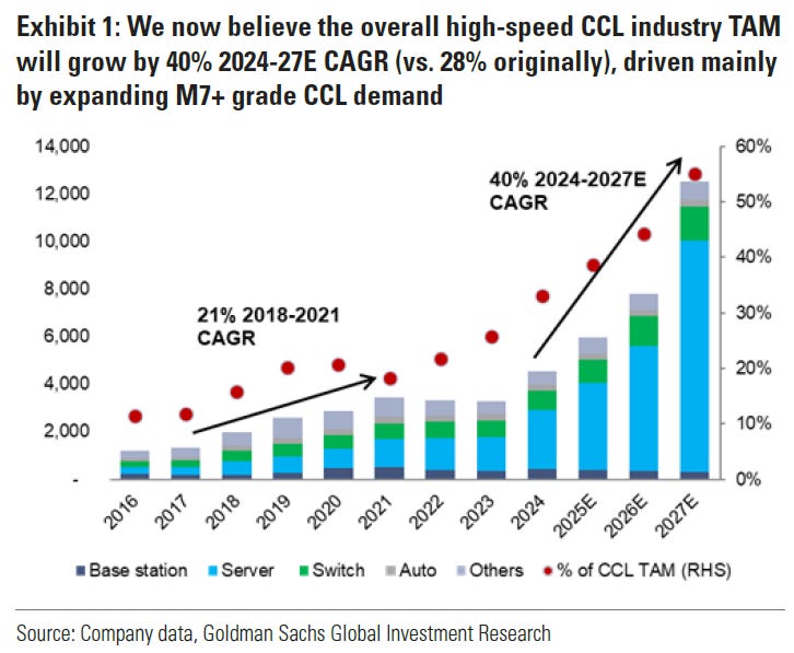
According to Goldman Sachs, the high-end CCL (Copper Clad Laminate) market is expected to consistently outperform the overall market in the coming years, with manufacturers cautiously expanding capacity amid an optimistic supply-demand outlook.
Expansion plans for high-end CCL manufacturers remain conservative in the next few years, with no large-scale capacity additions anticipated in the industry. As AI servers, 800G switches, and other high-end applications continue to raise performance requirements for CCL materials, existing production capacity utilization is expected to stay high. This cautious capacity expansion on the supply side may lead to a potential supply shortage in the high-end CCL market.

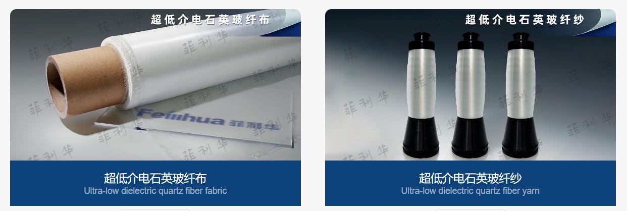
Hubei Feilihua Quartz Glass Co., Ltdis located in Jingzhou, a renowned historical and cultural city in Hubei Province, China. It is one of the few manufacturers in the world with mass production capabilities for quartz fiber and serves as a leading supplier of quartz fiber for the aerospace industry in China.
The company specializes in the R&D and production of high-performance quartz glass, quartz fiber, and related composite materials. Its products are widely used in high-tech sectors such as semiconductors, optical communications, photovoltaic solar energy, advanced optics, and aerospace. Feilihua is also thefirst quartz material supplier in Chinato be certified for use in integrated circuit (IC) manufacturing. The company possesses acomplete industrial chain, spanning from quartz fiber materials and 3D woven quartz fiber fabrics to composite structural components based on quartz fiber.
Leveraging its technological advantages in the quartz fiber field, Feilihua has entered the quartz fiber electronic fabric segment. In 2021, the company acquired a 60% stake in Zhongyi New Materials, a company established in May 2016 that focuses on the development, production, and sales of safe and environmentally friendly industrial fabrics. Its main products include electronic-grade glass fiber fabric, high-strength glass fiber fabric, carbon fiber fabric, graphene fiber fabric, and quartz fiber fabric, which are widely used in fire protection, insulation, thermal shielding, electronics, and aerospace applications.
Zhongyi New Materials possesses a wide range of composite fiber weaving technologies, surface treatment processes, and product delivery capabilities. Its engineering team has over 20 years of experience in the electronic fabric industry, further enhancing Feilihua’s competitiveness in high-end electronic textile markets.
Feilihua Quartz Fiber Electronic Fabric Development Timeline
Launched the ultra-low dielectric quartz electronic fabric project
First batch of quartz electronic fabric trial production
Feilihua acquired Zhongyi New Materials and delivered multiple samples for first-generation quartz fabric testing
First-generation quartz fabric successfully passed testing with Df reaching 0.00027 (2.7×10⁻⁴)
Initiated second-generation quartz electronic fabric development; further reduction of Df underway

Development Highlights of Second-Generation Ultra-Low Df Quartz Electronic Fabric
Zhongyi New Materials is actively advancing the development of its second-generation ultra-low dielectric loss (Df) quartz electronic fabric, aiming to support next-generation high-frequency applications with improved materials, process innovation, and scalable capacity.
Semiconductor-Grade Quartz Yarn
Proprietary Post-Treatment Process
Zhongyi has independently developed a proprietary post-processing technology, enabling better fiber-matrix interaction and reliability for high-frequency signal transmission.
Composite Surface Treatment Agent
The surface finishing process adopts acomposite silane-based treatment agent, further enhancing adhesion and surface uniformity, which is critical for achieving low-loss performance.
Expansion Roadmap:
Planned capacity: 1 million square meters/year
Commercial launch of the second-generation ultra-low Df quartz electronic fabric
Capacity target: 20 million square meters/year

Its wholly owned subsidiary, Taishan Fiberglass, is one of the most competitive integrated glass fiber enterprises in China, with products spanning high-, mid-, and low-end markets. Taishan Fiberglass is the third company globally and the first in China to mass-produce second-generation low-dielectric (Low-Dk) glass fiber fabric. It has also developed multiple types of low-expansion glass fiber fabrics, which have passed customer validation.
As of the end of 2024, the company had built four production lines dedicated to low-dielectric glass fiber. In 2024, Taishan Fiberglass sold 1.36 million tons of glass fiber and related products, generating RMB 7.74 billion in revenue, representing a 7.6% year-on-year decline. Net profit attributable to shareholders was RMB 370 million, down 63.3% from the previous year.
In April 2025, Zhongfu announced that its wholly owned subsidiary Taishan Fiberglass would invest RMB 1.428 billion (including RMB 555 million in reused assets) to build a specialty glass fiber fabric project with an annual capacity of 35 million meters. This project targets emerging application scenarios in key fields, aiming to achieve differentiated market competitiveness.
Taishan Fiberglass is focusing on glass fiber and its composite materials as its core business, Taishan Fiberglass built China’s first 10,000-ton-level tank furnace wire-drawing production line in 1997. After more than a decade of development, the company’s total annual output of glass fiber and related products has reached 600,000 tons, making it one of the top five glass fiber manufacturers globally and one of the top three in China.

Taishan Fiberglass’s main products include E-glass direct roving, chopped strand mat, woven roving, multi-axial warp-knitted fabrics for wind turbine blades, thermoplastic chopped fibers, thermoplastic long fibers, acid-resistant E-glass and boron-free TCR fibers, and electronic-grade fine yarns. These products are widely used across various sectors of the national economy, including construction, transportation, electronics and electrical appliances, and aerospace, and are exported to over 70 countries and regions, including the United States, Western Europe, Canada, the Middle East, and South Africa.

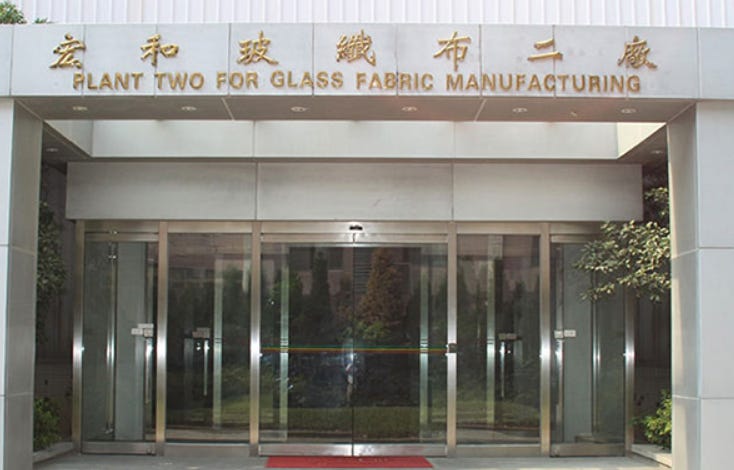
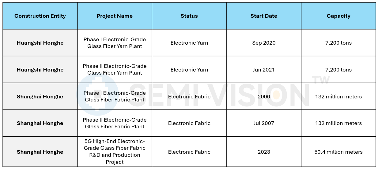
Grace Fabric (Honghe)is a high-tech enterprise specializing in the R&D, production, and sales of mid- to high-end electronic-grade glass fiber fabric. It is a globally recognized manufacturer in the mid- to high-end segment of the electronic-grade fiberglass fabric industry.
Its subsidiary, Shanghai Honghe, focuses on the production of electronic-grade fiberglass fabric, while Huangshi Honghe primarily produces electronic-grade fiberglass yarn. The company’s products have reached international technical standards and are exported to countries such as Japan, the United States, Europe, and Southeast Asia. Key downstream customers include Shengyi Technology, Unimicron, EMC, TUC Technology, and Nan Ya PCB.
In 2024, the company produced 202.83 million meters of electronic fabric, an 8.13% year-on-year increase. It sold 208.81 million meters, marking a 22.72% year-on-year growth.
From a revenue perspective, mid- and high-end fabrics together accounted for over 80% of total sales, with high-end fabrics (including ultra-thin and extremely thin types) accounting for 36% alone.


PreviousNext
TopLatestDiscussions








See all