From Taiwan to the World: Silicon Photonics Roadmap and Its Role in Global AI Infrastructure
From Taiwan to the World: Silicon Photonics Roadmap and Its Role in Global AI Infrastructure
- Source: SemiVision
- Author: SEMIVISION
- Published: 2025-07-25T22:57:21+08:00
- URL: https://tspasemiconductor.substack.com/p/from-taiwan-to-the-world-silicon From Taiwan to the World: Silicon Photonics Roadmap and Its Role in Global AI Infrastructure


From Taiwan to the World: Silicon Photonics Roadmap and Its Role in Global AI Infrastructure
Original Articles By SemiVision Research ( TSMC , MediaTeK , Nvidia , PIC Summit , PhotonDelta , SmartPhotonic ,Phix, FiconTEC)

Jul 25, 2025
∙ Paid
When analyzing MediaTek’s strategic positioning in ASICs, SerDes, and the CPO (Co-Packaged Optics) market, it is essential to return to the fundamental layer: the interconnect technology that underpins system scalability. As AI computing architectures continue to evolve, whether through scale-up or scale-out, the limitations of data transmission bandwidth and efficiency have become key bottlenecks to overall system performance.

Against this backdrop, optical interconnect technologies are emerging as critical enablers. Their inherent advantages—high bandwidth, low latency, strong EMI resistance, and low power consumption—align directly with the demands of next-generation AI and high-performance computing systems. Meanwhile, silicon photonics has increasingly been recognized as the ideal platform for realizing electro-optical integration, and is now being considered as part of both SoC design and advanced packaging strategies.
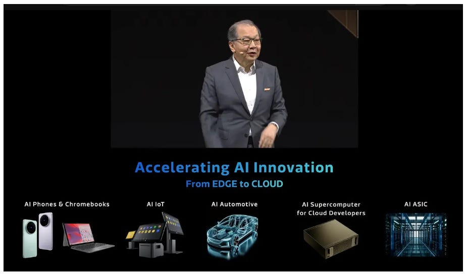
Source: Computex 2025
ForMediaTek, this transition is particularly significant in the context of Edge AI applications. Take smartphones as an example: achieving real-time, intelligent image and perception processing at the device level will depend on high-speed connections between sensors (such as CIS: CMOS Image Sensors) and the SoC or NPU. Traditional electrical interconnects like MIPI are approaching their physical limits, making the adoption of polymer-based optical interconnects a promising innovation path.

2025年5月21日
Such optical interconnect technologies are not only applicable to intra-device links between image sensors and processing chips, but also scalable to high-bandwidth, low-latency inter-chip connections within complex AI architectures. This opens a new frontier for MediaTek to drive differentiated system design and capture emerging market opportunities across AI-enabled mobile and edge platforms.

2025年6月28日
The adoption of Optical Interconnection technologies has imposed significantly higher demands on PCB (Printed Circuit Board) materials and structural design compared to traditional electrical interconnects. To enable the effective transmission of high-speed optical signals, PCB-integrated optical waveguide structures (such as polymer waveguides) must exhibit extremely low signal loss and stable phase control. This necessitates the use of substrate materials characterized by low dielectric constant (Dk) and low dissipation factor (Df).

2025年7月6日
In particular, when handling high-speed interfaces like 112G PAM4, 224G, or beyond, even minor signal attenuation or reflection can lead to a substantial increase in bit error rate (BER), thereby degrading overall interconnect quality. As a result, high-frequency materials such as M8 or M9-grade laminates (e.g., Rogers, Panasonic Megtron series, Shengyi SLP systems) have become essential components for implementing optical interconnects. The precision alignment of multilayer board structures with embedded waveguides also becomes increasingly critical.
2025年7月8日
Furthermore, these materials must demonstrate excellent thermal stability and mechanical reliability to support long-term stable transmission of polymer-based optical waveguides. In CPO (Co-Packaged Optics) or LPO (Linear-drive Pluggable Optics) architectures, the PCB must not only accommodate high-speed SerDes and optical engine modules but also support precise optical alignment and insertion structures. This requires stringent control over stack-up design, copper surface roughness, and coefficient of thermal expansion (CTE).
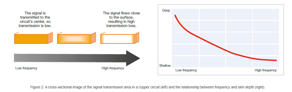
In high-frequency signal transmission within the GHz domain, the Skin Effect causes alternating current to concentrate near the surface of conductors, significantly reducing the effective current-carrying cross-section and thereby increasing conductor resistance. Additionally, copper surface roughness further exacerbates transmission loss, as the irregular copper surface forces current to travel along tortuous paths, increasing insertion loss and elevating the effective dielectric constant (Dk)—a phenomenon well-documented in experimental studies.

Transmission loss can be reduced by managing the roughness of the copper foil used in the circuits. While rough copper foil can increase transmission loss by scattering the signal, using circuits with concavities and convexities (roughness) smaller than the skin depth leads to a short signal transmission route, resulting in less signal loss
To support high-performanceOptical Interconnect (OI)systems, PCBs must offer more than traditional signal transmission capabilities; they must also accommodate high-density optoelectronic integration, placing stringent demands on both materials and structural design. First, the use of low Dk/Df materials such as M8 or M9-grade laminates (e.g., Rogers and Megtron series) is essential to reduce dielectric loss and shift the dominant frequency of conductor loss to higher ranges. Second, smooth copper surfaces are required to minimize energy loss caused by the Skin Effect. These can be achieved through electroplating or modified semi-additive process (mSAP), which enables the formation of vertical copper sidewalls with minimal roughness.
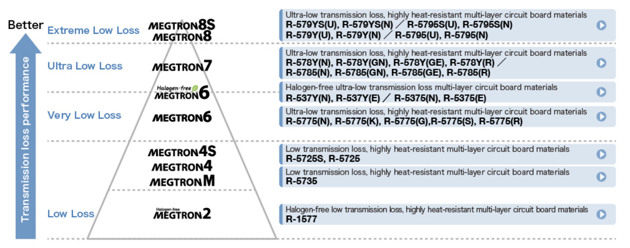
To further reduce frequency-dependent conductor losses, designers must adopt precise surface roughness modeling techniques such as the Hammerstad or Huray models, which are widely applied in signal integrity (SI) simulations. Structurally, multilayer PCB stack-ups must ensure precise alignment between polymer waveguides and copper traces, while effectively managing coefficient of thermal expansion (CTE) mismatches between dissimilar materials. For critical high-speed layers, reverse foil technology can be used to enhance copper surface flatness and SI performance.
For instance, AT&S’s 800G module-level PCBs have demonstrated micron-level trace precision and superior control over copper edge geometry, showcasing the high-end manufacturing capabilities required for next-generation interconnects.
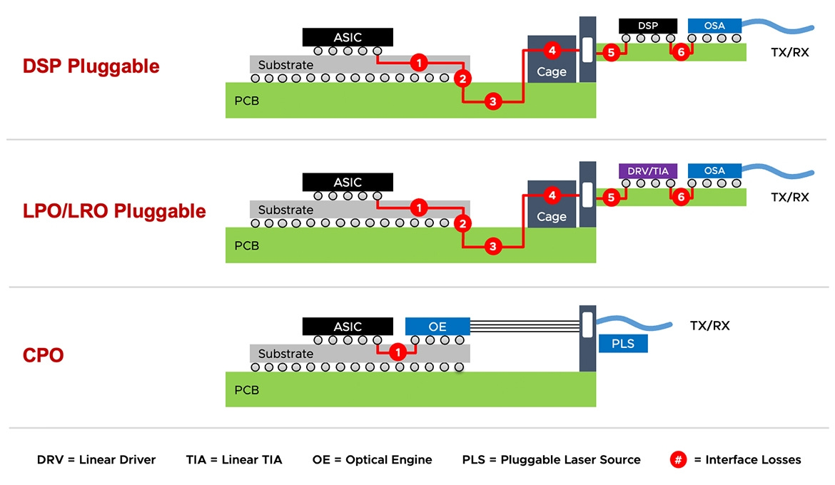
In high-speed and high-frequency signal design,Power Integrity (PI)andSignal Integrity (SI)face unprecedented challenges. As data rates surpass112G, 224G, and beyond, the signal cycle for each interface shrinks to just a few picoseconds. Under such tight timing margins, even the slightest power noise or signal degradation can lead to system errors or bit misinterpretation.
ForPI, thePower Delivery Network (PDN)must ensure a stable and low-noise power environment. This requires ultra-low impedance, robust decoupling strategies, and effective suppression of simultaneous switching noise (SSN) and resonances. However, at high frequencies, capacitive decoupling becomes less effective and parasitic inductance from PCB traces and vias rises, making power stability increasingly difficult to achieve.
On theSIside, high-frequency designs must contend with serious issues such assignal reflection, crosstalk, insertion loss, andtiming skew. Maintaining signal fidelity demands preciseimpedance control, optimizedtrace topologies, carefuldielectric material selection, and a comprehensive understanding ofpackage-induced distortions.
In heterogeneous integration and multi-die architectures, risingI/O densityand deeperpackage stackingintroduce additional signal interfaces, increasingtransition lossandtiming inconsistency. These requireadvanced simulation,materials engineering, anddesign co-optimizationto ensure stable transmission across the entire signal path.
Moreover, thePI-SI coupling effectcannot be ignored: high-frequency power noise may couple into signal traces, causingjitterand raising thebit error rate (BER). Therefore, in modern high-speed system design, PI and SI must be addressed as aco-optimized, unified problem. Only throughco-simulation,co-design, anddynamic testingcan engineers ensure reliable performance at operating frequencies beyond the GHz threshold.
As ASICs transition from the N3 process node to N2, the significant increase in transistor density drives parallel growth in compute units and I/O density within the chip. This leads to a sharp rise in overall power density and transient power demands. Against this backdrop,advanced packaging technologies—such asCoWoS, SoIC, and EMIB—must not only support more complex die integration but also incorporateIntegrated Voltage Regulators (IVRs)to enable near-core power delivery. IVRs help minimize power loop lengths, suppressIR dropanddynamic voltage droop (DvD), thereby enhancing bothPower Integrity (PI)andSignal Integrity (SI).
However, at thePCB level, traditionalsurface-mounted MLCCs(Multi-Layer Ceramic Capacitors) are increasingly inadequate for meeting the fast transient current demands and noise suppression requirements of high-frequency N2-generation ASICs. As a result, many high-end system designs are turning toembedded MLCCtechnology, where capacitors are integrated directly into inner PCB layers. This reduces inductive paths and parasitic effects, maintaining strong decoupling performance even at GHz frequencies. Embedded MLCCs complement IVR modules in sustaining robust PI and also positively contribute to SI by stabilizing voltage across high-speed I/Os.
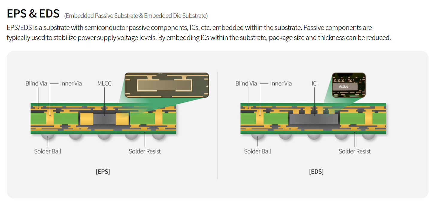
Source: Samsung
Overall, PI and SI are no longer just back-end considerations, but fundamental design drivers that impact system-wide performance and stability. The N2 era will accelerate the adoption of IVR and embedded MLCCs as essential components of high-frequency, high-density ASIC systems.
In future high-performance computing platforms, the competition will not be between standalone chips, but betweenintegrated systemscomposed ofASIC design, advanced packaging, co-packaged optics (CPO), and high-end PCBs. As semiconductor technology advances into the N2 node, the simultaneous increase in transistor density and power consumption exacerbates PI/SI challenges. These challenges must be addressed by embedding IVRs within the package for near-core power delivery and adopting embedded MLCCs in the PCB to reinforce power stability.
Meanwhile, CPO modules demandultra-low-loss, high-speed electro-optical interconnects, further raising the bar for PCB material selection (e.g., low-Dk/Df materials like M8 and M9),skin effect control(e.g., smooth copper and reverse foil technologies), andtrace roughness management. In this trend, only bytreating the chip, packaging, optical interconnects, and PCB as a unified, co-optimized system architecture, can we deliver the high-speed, low-power, and highly reliable compute platforms needed for the AI and data-centric era.
This is thedefining direction for future system-level innovation.
As the industry moves toward448G SerDesand beyond, the demands onPower Integrity (PI)andSignal Integrity (SI)are escalating rapidly.Optical Engines—central to next-generation AI and data center platforms—require extremely stable power delivery and clean signal pathways. These engines are highly sensitive to noise, insertion loss, jitter, and impedance mismatches, especially in high-density, high-speed co-packaged environments. While current112Gand224GSerDes implementations are feasible on platforms like TSMC, the transition to448Gexposes new challenges in CMOS scalability, pushing the limits of traditional semiconductor and packaging techniques. For countries and suppliers, this presents a rare opportunity to enter the high-frequency, optical interconnect race—missing this wave could mean losing long-term strategic positioning.
In this context,silicon photonicshas emerged as a globally contested technology. Countries likethe Netherlands, the UK, the Czech Republic, Germany, Spain, Belgium, Switzerland, and Franceare actively investing in silicon photonics development, with a shared vision to establish end-to-end supply chains across materials, design, fabrication, testing, and system integration.
TFLN Platform and the CCRAFT/ELENA Programs
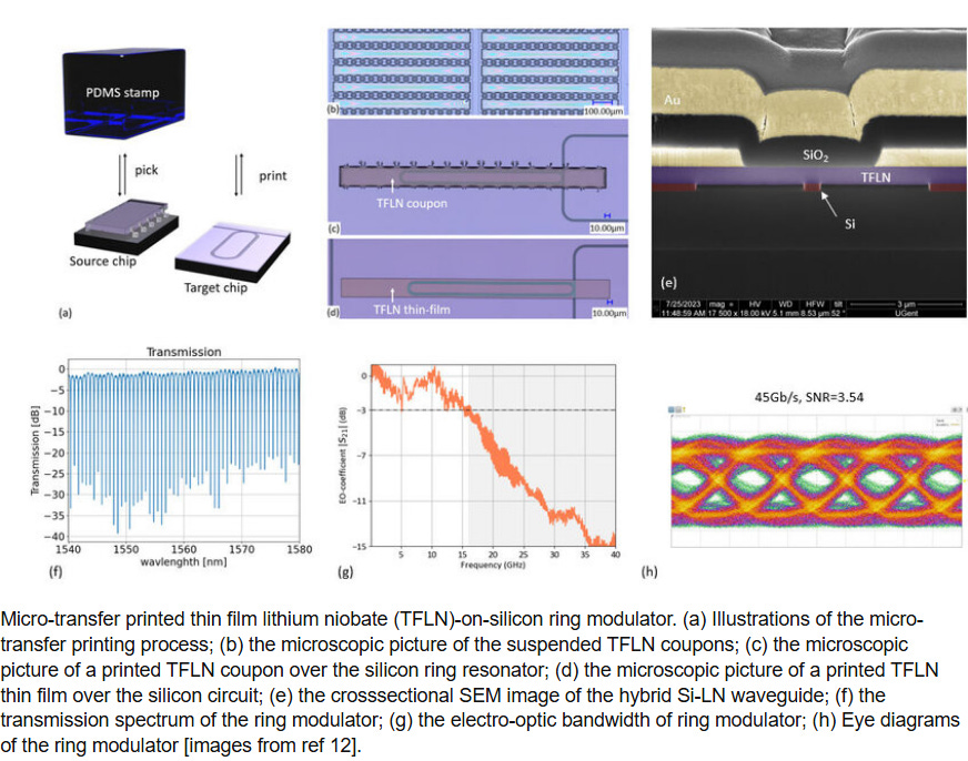
Europe’s cutting-edge efforts inThin-Film Lithium Niobate (TFLN)are led by initiatives such asCCRAFT Foundryand theELENA project, which aim to build a CMOS-compatible high-performance modulator platform for next-gen optical interconnects. Key participating institutions include:
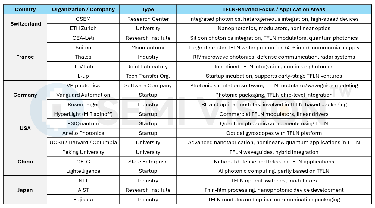
This consortium spans the entire ecosystem—from materials (e.g., Soitec’s TFLN-on-insulator substrates) to photonic design automation, packaging automation (e.g., Vanguard), and final module integration for optical communications and quantum applications.

Taiwan’s Strategic Push into TFLN: Foxconn Research Institute Leads the Charge
Although Taiwan entered the field of TFLN (Thin-Film Lithium Niobate) relatively late, it has begun to demonstrate strategic foresight and an active deployment posture. A key player in this transformation is the Foxconn Research Institute, whose technology roadmap spans multiple cutting-edge domains, including:
Dual-Track Development of TFLN and SOH (Silicon-On-Hybrid)
Foxconn Research Institute is actively developing the next-generation silicon photonics platform, leveraging the high-speed modulation capabilities of TFLN and the field-effect gain advantages of SOH. The goal is to overcome the current limitations of silicon photonics in nonlinear optics and ultra-fast modulation, with targeted applications in AI/HPC, quantum communication, and high-frequency sensing.
Advancements in Nonlinear Optics
The research team is deeply exploring TFLN’s second-order nonlinear coefficient (χ²) and ultra-low-loss waveguide properties to enable on-chip frequency conversion, optical parametric amplification (OPA), and entangled photon generation. Their work aligns with the global LNOI (Lithium Niobate on Insulator) technology roadmap, while also actively investigating hybrid integration and advanced packaging methods.
Optoelectronic Integration and Packaging Strategy
In collaboration with domestic and international universities and packaging material suppliers, the institute is addressing the thermo-mechanical stress challenges of integrating TFLN chips with silicon-based circuits. It is also evaluating the feasibility of using LNOI-based modulators in co-packaged optics (CPO) platforms.
Extension to Power Device Technologies
Beyond photonic chips, Foxconn Research Institute is also developing manufacturing and packaging technologies for wide-bandgap power devices such as SiC and GaN. These efforts are part of a broader strategy targeting electric vehicles and power management systems, forming a cohesive “photonics-electronics-thermal” integration approach.
Foxconn’s ambition is to utilize heterogeneous material platforms (e.g., TFLN, SOH, SiN) to synergize Taiwan’s strengths in semiconductor fabrication, advanced packaging, and materials science, thereby establishing a deep technological foundation for the future of silicon photonics and power semiconductor systems. This strategy not only enhances Taiwan’s influence in the global photonic IC supply chain, but also gives Foxconn new technological leverage in its AI, automotive, and high-speed communication applications.
Silicon Photonics for Automotive Networks: An Emerging Frontier
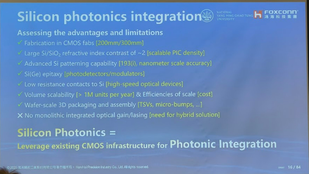
A core focus for the Foxconn Research Institute is the practical deployment of silicon photonics.
The current automotive network architecture is undergoing a disruptive transformation. With the rapid evolution of electric and autonomous vehicles, traditional copper-based data transmission can no longer meet the growing demands for high bandwidth, low latency, and high reliability. Emerging architectures like SiPhON (Silicon Photonics-based Optical Network) represent the future, integrating central compute platforms and zonal gateways via optical backbone networks.
Within this setup, silicon photonic-based optical modules—incorporating LDs, MDs, and PDs—enable high-speed in-vehicle data transmission across the C-plane (1.25/2.5 Gbps) to D-plane (up to 25 Gbps). These modules offer exceptional EMC, electrical isolation, environmental adaptability, and mechanical flexibility. Compared to conventional copper cables, optical fibers exhibit superior fatigue resistance and installation flexibility, making them ideal for the increasingly complex sensor and control networks in modern EVs.
Recognizing this trend, Foxconn is actively aligning its technology portfolio. Its research into TFLN and SOH platforms aims to compensate for silicon photonics’ limitations in nonlinear performance and modulation speed. Early-stage development is underway for high-speed modulators, frequency converters, and optical parametric amplifiers, which can be deeply integrated into automotive systems like SiPhON.
Toward Vertical Integration in Automotive Connectivity
Foxconn’s automotive strategy extends beyond chip and module development to include vertical integration of the entire connectivity solution. The company has long-standing expertise in connector design, automotive modules, and cable harness manufacturing. Looking ahead, integrating auto-grade fiber (AGF) into in-house packaging and plug-and-play module designs may enable Foxconn to build a proprietary optoelectronic supply chain, seizing the core value of next-generation vehicle networks.
MIH Alliance: A Platform for Optical Architecture Deployment
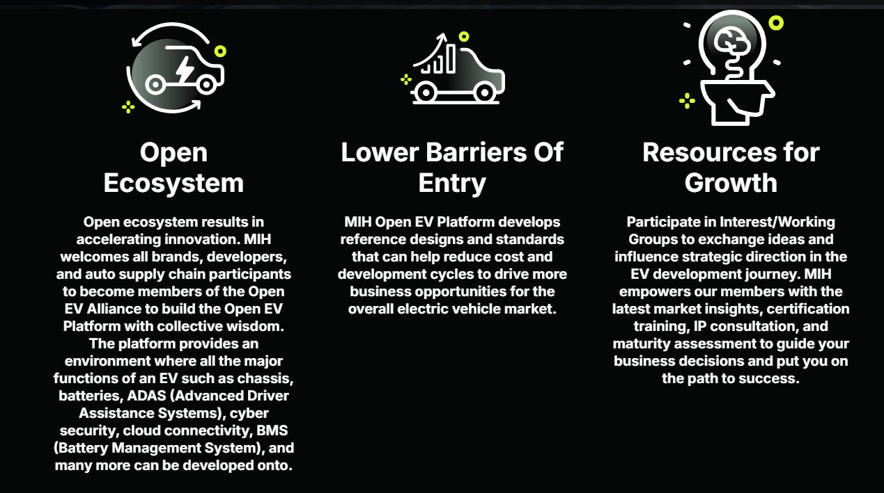
Through the MIH Alliance, which advocates software-hardware decoupling and modular system design, Foxconn holds a unique position to introduce optical communication architectures at the vehicle system level. Should it succeed in commercializing self-developed SiPh + TFLN modulators, and implementing them via reliable packaging technologies (e.g., COBO, CPO, NPO) for zonal gateway interconnects, Foxconn could lead Taiwan into the core of the global automotive optical communication industry chain.
From OEM to System Architect: Foxconn’s Strategic Evolution
This comprehensive initiative reveals Foxconn’s transition from a contract manufacturer to a strategic supplier with proprietary technologies and the ability to define system-level specifications. As vehicles become increasingly intelligent, mastering the in-vehicle optical backbone will be essential for ensuring compute performance, safety feedback, and sensor integration. Foxconn now stands at the inflection point of this industry transformation.
TFLN and Polymer: Two Pillars of Nonlinear Photonics Innovation
There are two primary paths in nonlinear photonics: TFLN and polymer-based platforms. Foxconn Research Institute is actively investing in both. While numerous overseas startups are advancing polymer-based solutions, the future of silicon photonics depends on integration with advanced packaging, heterogeneous integration, and bonding technologies—domains where Foxconn plays a critical bridging role between industry, academia, and real-world deployment.
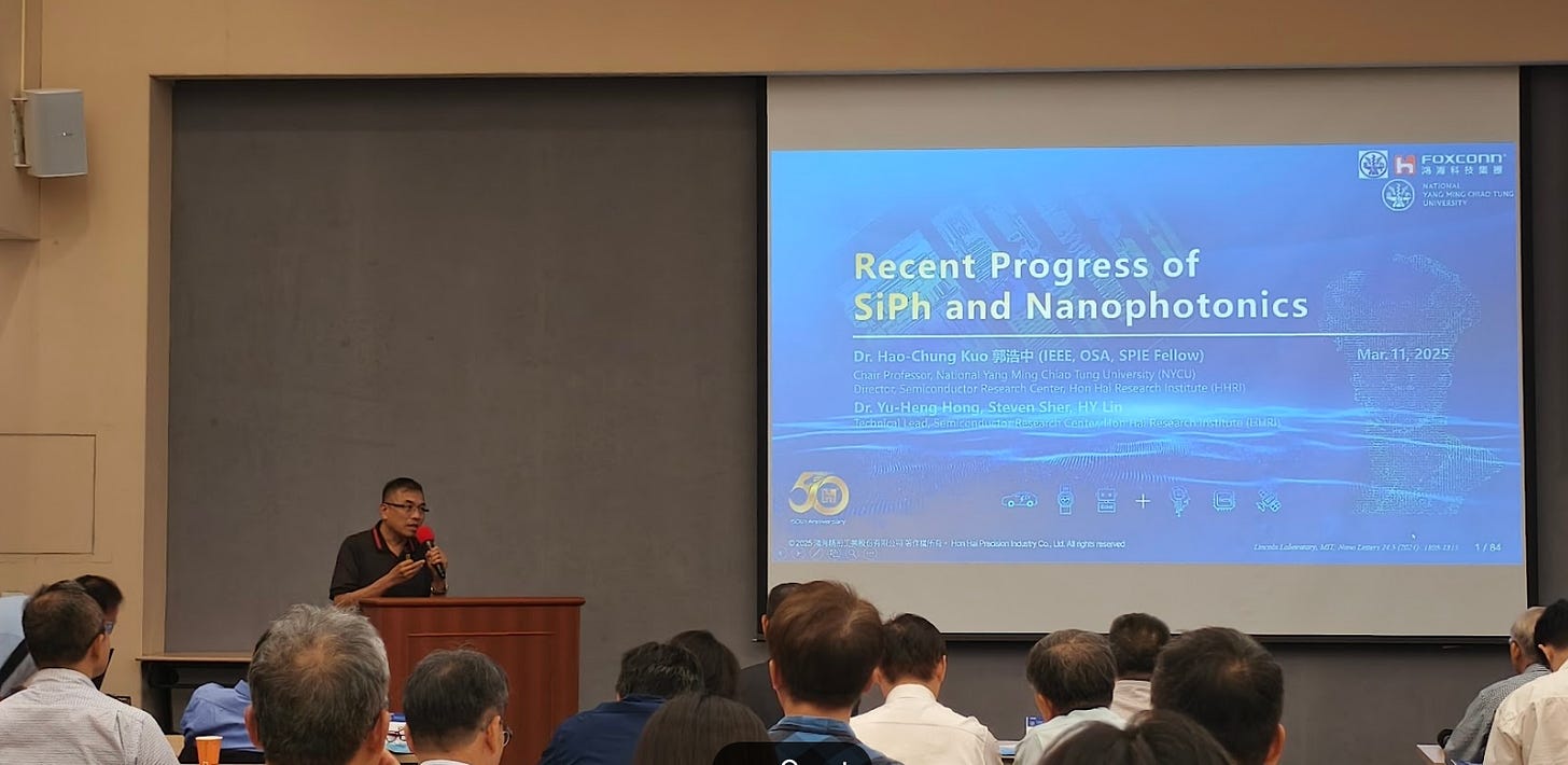
Currently, Taiwan’s leading expert in silicon photonics, Prof. Hao-Chung Kuo from NYCU, is guiding the technical development, with Foxconn Research Institute playing a central role in realizing these innovations at scale.


2025年6月20日
One of the most promising rising stars in the European silicon photonics landscape is the Netherlands. Currently, the country is actively developing a comprehensive silicon photonics supply chain centered around Eindhoven, positioning itself as a key player in the global photonics industry. The Netherlands is set to participate in a series of high-profile activities atSEMICON Taiwan 2025, highlighting its advancements and collaboration opportunities. In addition, a number of dedicated discussions and events focused on silicon photonics are scheduled for August, offering valuable insights into the future of this critical technology.
The Netherlands: Dual-Track Silicon Photonics Strategy
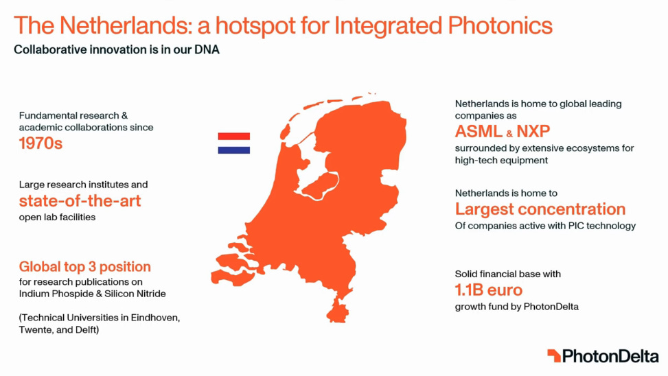
The Netherlands is a model of“technology platform + application-driven”deployment, anchored inEindhovenand coordinated by thePhotonDeltaalliance. Its silicon photonics ecosystem features:

Academic & R&D: Eindhoven University of Technology (TU/e) and University of Twente provide core research and talent.
Foundry Services: SMART Photonics, one of the few dedicated pure-play silicon photonics fabs in Europe.
Design & Packaging: Lionix International for photonic circuit design, and Phix for advanced photonic packaging and automated alignment.
Application Domains: Extends across AI interconnects, FMCW LiDAR, quantum photonics, biomedical sensing, and more.

PhotonDelta integrates these capabilities into a comprehensive and exportable silicon photonics platform, positioning the Netherlands as a continental hub for scalable photonic innovation.
Multi-Nation Collaboration Building Europe’s Photonics Leadership
Beyond the Netherlands and Switzerland, countries like:
The UK: with initiatives such as the Compound Semiconductor Applications Catapult and photonic quantum computing platforms.
Germany: through Fraunhofer IPT and KIT, focusing on hybrid integration and photonic testing.
The Czech Republic: leveraging its laser optics and packaging expertise.
Belgium & France: imec and CNRS jointly advancing silicon photonic design automation and next-gen materials.
Together, these programs are constructing a pan-European photonics corridor that blends research, manufacturing, and commercial application.
As 448G and optical interconnects redefine system architectures,Europe’s strategic investments in silicon photonics, TFLN platforms, and advanced packagingare enabling it to become a leader in electro-optical system integration. To meet the PI/SI challenges of next-generation AI workloads and ultra-high-speed data flows, only those who masterchip–package–PCB co-designwith deep expertise in materials, thermal management, and signal integrity will define the future of computing infrastructure.
【Event Preview|SEMICON Taiwan 2025 Silicon Photonics Forum】
In an era where AI computing, quantum communications, and high-performance interconnects are accelerating in demand,Silicon Photonicsis rapidly emerging as a transformative technology driving the next wave of semiconductor innovation. In 2025,SEMICON Taiwan will proudly host theSilicon Photonics Forum, focusing on the latest global breakthroughs, supply chain development, and international collaboration opportunities in this critical domain.

The forum will bring together world-leading experts and industry pioneers to explore theentire value chain of silicon photonics, fromPIC (Photonic Integrated Circuit) design, fabrication, packaging, and testing to emerging applications.
In addition, the international exhibition pavilions are also a must-see highlight.
European Silicon Photonics Ecosystem Makes Its Taiwan Debut
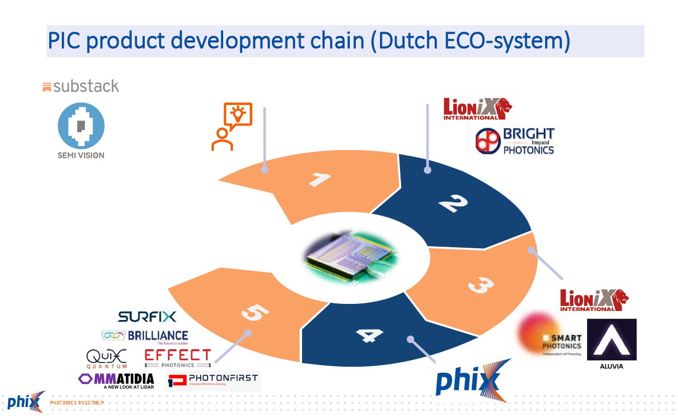
For the first time, leading organizations from the Netherlands—includingPhotonDelta, SMART Photonics, and Phix—will be on-site in Taiwan to share their strategic efforts in photonic platform development, packaging processes, and system-level deployment.
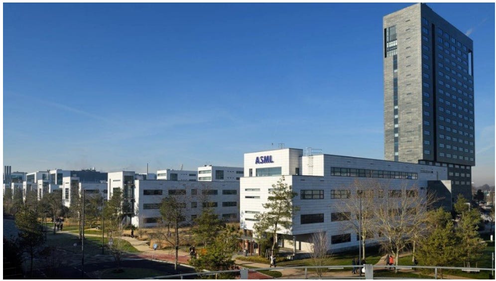
Following the global success of ASML as a dominant force in semiconductor equipment, the Netherlands is now cultivating its next strategic technology frontier. At the heart of this momentum liesEindhoven, often hailed as the“Silicon Valley of Europe”, which is rapidly emerging as a global hub forSilicon Photonics.

Eindhoven boasts a robust technological infrastructure and a thriving innovation ecosystem. It is not only the birthplace of world-renowned semiconductor giants such as ASML and NXP, but also a magnet for cutting-edge photonics startups, research institutes, and deep-tech alliances. The region supports a vertically integrated supply chain that spans silicon photonics (SiPh) foundry services, advanced photonic packaging and alignment, EDA design platforms, and end-system applications in fields such as quantum computing, next-generation communications, and AI photonic accelerators.
At the heart of this ecosystem is the Eindhoven University of Technology (TU/e), which plays a critical role in driving innovation across the semiconductor value chain. TU/e is globally recognized for its research excellence in photonic integration, heterogeneous packaging, and nanoscale fabrication, and maintains strong collaborations with both industrial leaders and emerging ventures. The university's interdisciplinary programs in electrical engineering, applied physics, and nanotechnology cultivate top-tier engineering talent, while its close proximity to High Tech Campus Eindhoven ensures seamless knowledge transfer from lab to fab. TU/e also contributes to several EU-led initiatives in PIC (photonic integrated circuit) development and advanced semiconductor prototyping, cementing its role as a key academic engine for Europe's semiconductor future.

This industry maturity will culminate at thePIC Summit Europe 2025, taking place fromNovember 3rd to 7th, where the full spectrum of the European photonic ecosystem will converge.
Why Attend?
Insights straight from the source– Get the latest insights on market and technology developments, helping you navigate the future of PICs with confidence.
Discover real-world applications– Learn which applications are proving most successful, and where the next big opportunities in photonics lie.
Meet key stakeholders– Connect with the most influential players in the industry, from technology leaders to business innovators and investors.
Shape the future of PICs– Gain direction on how to scale your business and technology while aligning with industry-wide efforts. Unlock collaboration opportunities – Whether you're looking for investment, partnerships, or technical cooperation, this is the place to make it happen.

Japan–Taiwan Strategic Cooperation on Photonic Supply Chain
Japanese and Taiwanese players will publicly unveil their collaborative roadmap on photonic wafer manufacturing, heterogeneous packaging integration, and end-use application deployment—aiming to establish Asia’s next photonic manufacturing powerhouse.
Startup × Academia: Live Demonstrations of Next-Gen Photonic Applications
FromAI model acceleration and optical switchingtonext-generation sensing chips, this session will showcase how photonic technologies are reshaping the infrastructure of AI and next-gen communication.
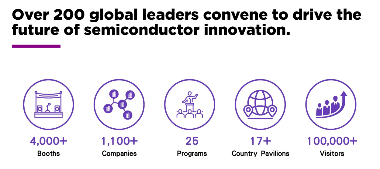
This year’sSEMICON Taiwanis set to hit a new milestone, featuring arecord 17 Country Pavilions, underscoring the strong momentum and international enthusiasm for global semiconductor and photonics cooperation. Confirmed countries and regions include:
Australia (New South Wales)
Japan
United Kingdom (UK Pavilion)
South Korea
United States(for the first time with a dedicated U.S. Pavilion, organized by AIT)
The Netherlands(coordinated by High Tech NL Semiconductors)
Taiwan Pavilion
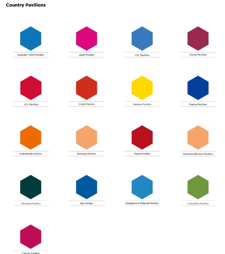
Other confirmed pavilions:China, Greater China Region, European Union Joint Pavilion, Malaysia, Poland, Singapore, Vietnam, and more to be announced—totaling 17 national pavilions.
Join us atSEMICON Taiwan2025 to discover how photonics is illuminating the future of computing, communications, and sensing.

Leading Global Silicon Photonics Companies You Must Know: Broadcom and Marvell
Broadcom
Broadcom stands at the forefront of Silicon Photonics and Co-Packaged Optics (CPO) technologies. ItsBailly CPO solutionexemplifies advanced optoelectronic integration by embedding bothPhotonic Integrated Circuits (PICs)andElectronic Integrated Circuits (EICs)within optical engine modules. These engines are directly co-packaged with high-density SerDes bump arrays onto switching ASICs, enabling ultra-high-speed optical I/O with minimal signal degradation.
For example, the Bailly platform based on theTomahawk-5 ASICintegrateseight 6.4 Tbps optical engines, delivering an aggregate51.2 Tbps of optical bandwidth, while reducing insertion loss by nearly80%compared to traditional pluggable modules.
Broadcom is also aggressively advancing itsSerDes roadmap to 200 Gbps/lane and beyond, supporting FR4 materials and bidirectional optical modulation. Its core strategy focuses ontight co-integration of SerDes, PICs, and ASICs, significantly shortening interconnect paths, enhancing signal integrity, and enabling compact thermal-aware system design.
Marvell
Marvell has also established a strong and competitive position in the silicon photonics space. Following itsacquisition of Inphi, Marvell now plays a critical role in high-speed SerDes, PAM4/coherent DSPs, TIAs, and optical module design.
Its recently launched3D SiPho optical engineis the industry’s first to integrate over32 lanes of 200 Gbps electro-optical channels, delivering6.4 Tbps total bandwidthper chiplet. The platform includes in-house designed components such as DSPs, TIAs, modulators, and microcontrollers, and achieves~30% improvements in energy efficiency and power reduction per bit. Marvell expects this architecture to serve not onlypluggable transceivers, but also futureCPO deployments, powering customAI accelerators (XPUs), high-frequency interconnects, and hyperscale cloud infrastructure.
Together, Broadcom and Marvell define the dual axis of leadership in silicon photonics innovation.While Broadcom emphasizeshigh-density CPO integrationand bandwidth scaling, Marvell focuses onmodular design, commercial viability, and scalable deployment. As the industry moves toward the448G SerDes era, the integration ofPICs, EICs, and SerDesby these two players is setting the benchmark fornext-generation optical interconnects and AI infrastructure platforms.

For Paid Members , SemiVision will discuss topics on
Optical Interconnect × CIS × Smartphone: Enabling a New Era of Sensor-Compute Integration for Edge AI
Rearchitecting AI Data Centers: The Shift to Optical Interconnects
The Rise of Scale-Up Architectures and Hybrid Interconnects in AI Data Centers
SerDes Battlefield Heats Up: MediaTek Targets 448G to Tackle the Next Frontier in High-Speed Interconnects
Redefining AI Interconnects: From Copper to Co-Packaged Optics
Breaking the Bandwidth Wall: Why Co-Packaged Optics Is Critical for AI-Era Interconnects
Optimizing Interconnect FOM: MediaTek’s Strategy for Scalable AI Infrastructure
MediaTek’s Optical Interconnect Roadmap: From Pluggable Optics to CPO
The Transition from Traditional Electrical Interconnects to Co-Packaged Copper (CPC) for 400G Transmission
Integrating Electrical and Optical Subsystems in XPU/AI Architectures: Challenges and Strategic Implications
MicroLED Optical Links: A Scalable, Low-Cost Alternative to Traditional Laser-Based Interconnects
Interconnect Innovation at the Core of AI and Cloud Data Center Performance
MediaTek’s Latest Developments in Optical Interconnects and Co-Packaged Optics (CPO) for AI/HPC Systems
-
Optical Interconnect Integration and Co-Packaged Optics (CPO) in AI/HPC Chips
-
Collaborative Ecosystem and Strategic Positioning in Optical Interconnects
-
R&D Investment in microLED and Optical Engine-Based Transmission Solutions
-
Technical Strategies and AI xPU Platform Development to Address Scale-Up/Scale-Out Demands in AI Data Centers
-
Technology Optimization for Edge AI Devices: Voice Assistants, Smart Home Hubs, and AI Tablets
-
Advanced Packaging Strategies (CoWoS, EMIB, SoIC) and Their Role in Optical Interconnects and CPO Deployment
Optical Interconnect × CIS × Smartphone: Enabling a New Era of Sensor-Compute Integration for Edge AI
As mobile devices evolve toward AI-driven perception, immersive experiences, and multimodal interaction, imaging and sensing modules have become critical to smartphone computing architectures. However, existing electrical interconnect solutions are approaching performance bottlenecks. Overcoming the limitations between sensing and compute domains is now a vital challenge for the next wave of innovation. In this context,optical interconnect technologyis emerging as a promising solution—particularly when integrated withCMOS Image Sensors (CIS)—showing substantial technical feasibility and commercial potential.
- Motivation: The Bottleneck Between Sensing and Computing Is Emerging
Modern flagship smartphones are pushing imaging systems toward100MP+ resolutions,multi-camera synchronization, andspatial-depth fusion. This results in dramatically increased data throughput per second. With the growing demand for 4K/8K video, multi-angle real-time fusion, and AI-assisted processing, data transmission bandwidth and latency are critical.
Conventional electrical interfaces such asMIPI D-PHY/C-PHYare nearing their physical limits in supporting the increasing volume and speed of data while maintaining power efficiency and signal integrity. These interfaces rely on tightly spaced high-speed traces, which place tremendous pressure on layout, power delivery, and thermal integrity within tight form factors.
Furthermore,Edge AI applicationslike real-time facial recognition, 3D spatial mapping, semantic vision, and AR/VR interaction require faster, more stable, and power-efficient interconnects between sensor modules and SoC or NPU blocks. Optical interconnects, with theirinherent advantages in bandwidth, latency, EMI immunity, and power efficiency, are ideally suited to address these next-generation requirements.
- Implementation Strategy: Polymer-Based Optical Interconnect for CIS Integration
One of the most viable approaches today is the use ofpolymer waveguidesas a medium for short-reach, chip-to-chip optical transmission. These flexible optical materials arethin, integrable within package layers, and bendable, making them particularly well-suited for space-constrained mobile environments.
In a practical implementation, the polymer waveguide can be placed between theCIS module and the Image Signal Processor (ISP), replacing MIPI electrical interfaces. With the integration ofmicro VCSELs (Vertical-Cavity Surface-Emitting Lasers)orμLEDsas light sources, this setup can enable short-reach, high-bandwidth, and low-power optical transmission.
Additionally, coupling this approach with advanced packaging technologies such asTSMC InFO, SoIC-In, orIntel Foverosenablesheterogeneous integrationof photonic components, sensor chips, and SoC cores. This not only shortens the interconnect path but also improves power and signal integrity across the system.
Beyond the CIS-ISP link, polymer waveguides can also be extended to support high-speed interconnects in multi-die SoC systems—for instance, SoC-to-NPU or SoC-to-AI co-processors—thus establishing a scalable interconnect fabric for future AI-centric mobile platforms.
- Engineering Challenges and Technical Barriers
Despite the compelling benefits of polymer-based optical interconnects, several engineering and manufacturing challenges remain before mass adoption in smartphones becomes feasible:
Spatial and Thermal Constraints
Smartphones have extremely limited internal space, and components like sensors, batteries, antennas, and SoCs are densely packed. Integrating optical elements requires precise module reconfiguration and optimized thermal management for light sources such as VCSELs or μLEDs.
Alignment and Manufacturing Precision
The performance of polymer waveguides depends heavily onsub-micron alignmentbetween light sources and receivers to minimize insertion loss and maximize signal fidelity. Achieving such precision in high-volume production requires advanced optical alignment and bonding technologies.
Material Stability and Reliability
Polymer materials are susceptible to environmental factors such as moisture and thermal aging, which may affect their optical index, shape, and transmission properties over time. Additional encapsulation, thermal cycling, and reliability testing are needed to ensure robust long-term operation.
CMOS Compatibility and Heterogeneous Integration
Most current optical components (e.g., VCSELs, photodetectors) are based on III-V materials. Integrating these into CMOS process flows or co-packaging them with silicon chips requires mature heterogeneous integration platforms and advanced wafer-level photonic packaging capabilities.
- Outlook and Strategic Implications
In summary, integrating optical interconnects into smartphone CIS architectures represents atransformative opportunity with significant potential and technical complexity. If the materials, packaging, and alignment challenges can be overcome, optical interconnects will become a key enabler for next-generation sensor-compute architectures. Companies likeMediaTek, Sony, Lumentum, and TSMC—those with expertise in photonic packaging, polymer interposers, and SoC integration—are well-positioned to define industry standards and lead the evolution of mobile imaging and AI systems.
Rearchitecting AI Data Centers: The Shift to Optical Interconnects
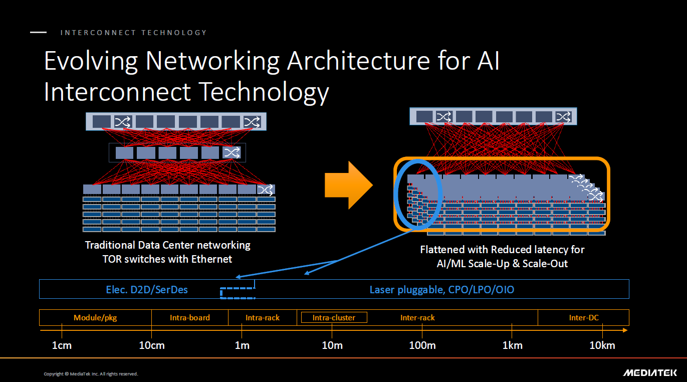
In the AI era, network architectures are rapidly evolving. Traditional data centers have long relied onTop-of-Rack (TOR) switchesand hierarchical Ethernet-based architectures. While these systems offer a degree of scalability, they are increasingly strained under the demands of large-scale AI/ML workloads—particularly with respect tolatencyandbandwidth limitations.
To address these challenges, data centers are transitioning towardflattened network architectures, which reduce the number of layers and shorten interconnect distances. This architectural simplification lowers latency and enhances thescale-up and scale-out efficiencyof AI models.
This trend is accelerating the shift from conventional electricalDie-to-Die (D2D)andSerDesinterconnects towardhigher-bandwidth, lower-power optical interconnect technologies, such asCo-Packaged Optics (CPO),Linear Pluggable Optics (LPO), andOptical I/O (OIO). These solutions enable optical interconnects to be deployed across a wide range of transmission distances—fromcentimeter-scale on-package linkstokilometer-scale data center fabrics—forming the foundation of next-generation AI computing infrastructures.
In particular, as AI clusters and hyperscale data centers continue to grow, these optical technologies will be critical in deliveringgreater energy efficiencyandoptimized resource allocation, making them a central pillar of future AI infrastructure development.

The Rise of Scale-Up Architectures and Hybrid Interconnects in AI Data Centers
As AI-driven computing demands continue to grow rapidly, data centers are facing a critical decision betweenScale-UpandScale-Outarchitectural strategies. Traditionally, performance improvements relied onhorizontal scaling (Scale-Out)—increasing the number of server nodes to boost aggregate compute power. However, to reduce latency and improve system-level efficiency, a significant shift towardvertical scaling (Scale-Up)is underway.
By 2028, it is projected that the bandwidth requirements for Scale-Up architectures will be10 times higherthan those of Scale-Out systems, presenting formidable challenges for both electrical and optical interconnect technologies.
This trend is also reshaping chip architectures, driving a transition towardI/O disaggregationandmulti-compute die integration. AI accelerators (such as GPUs, NPUs, and ASICs) are moving away from monolithic designs and instead adoptingmulti-die configurations, where compute chips are interconnected viahigh-speed I/O modulesto maximize performance density and data transfer efficiency.
For AI data centers, the future focus will lie in designingoptimized interconnect architectures—leveraginghybrid approaches that combine electrical and optical channels. This will be key to enabling higher Scale-Up connection densities and achieving lower latency, forming the foundation for competitive advantages incustom chip design and advanced packaging.

SerDes Battlefield Heats Up: MediaTek Targets 448G to Tackle the Next Frontier in High-Speed Interconnects
The platform also supports multipleForward Error Correction (FEC)schemes, enabling adaptive optimization based on varying channel conditions. This ensures robust reliability in high-frequency environments across a range of applications, includingChip-to-Chip (C2C)communication andClock and Data Recovery/Digital-to-Analog Conversion (CR/DAC).
This indicates thatMediaTekis actively building foundational interconnect capabilities tailored for thescalability demands of future AI and data center infrastructures, while simultaneously establishing a strategic position inhigh-speed SerDes and co-design for advanced packaging.
1.Cutting-edge 224 Giga‑baud SerDes
In October 2024 at the OCP Global Summit, MediaTek demonstrated theirsilicon-proven long‑reach 224G SerDes, targeting high-performance ASIC systems. This represents a significant leap from their existing 56G and 112G SerDes solutions, showcasing substantial improvements in bandwidth, reliability, and power efficiency .
2.Next-gen ASIC Platform with Optical Integration (CPO)
At OFC 2024, MediaTek introduced a next-generation ASIC design platform featuringheterogeneous integration of both high-speed electrical I/O (via SerDes) and co-packaged optics (CPO). The demo showcased an 8×800G hybrid electrical/optical setup, which reduces board space, cuts costs, doubles bandwidth density, and lowers power consumption by around 50% compared to traditional configurations .
3.Proven 112G Long‑Range SerDes
Back in November 2019, MediaTek introduced its112G long-range SerDes IPin a 7nm process, supporting PAM4 and NRZ signaling, various IEEE standards (1/10/25/50/100 G), and advanced diagnostics. This IP has been silicon-proven, reinforcing MediaTek’s SerDes credentials .
4.Comprehensive SerDes Portfolio & Roadmap
MediaTek has built a full SerDes IP stack—from 10G and 28G to 56G, 112G, and now 224G—with R&D reportedly underway for448G SerDes. Their platform leverages advanced process nodes (2–3 nm), next-gen packaging, and power optimizations enabled by DTCO (Design Technology Co‑Optimization) .
5.Collaborations & Ecosystem Development
MediaTek has partnered with companies likeRanovus(for co-packaged optical engines),Foxconn Interconnect Technology(for CPO development), and has fielded demonstrations including UCIe/tile-based die-to-die interconnects and die-to-die PHYs at 20 Gbps .

Redefining AI Interconnects: From Copper to Co-Packaged Optics
From the perspective of energy efficiency and transmission distance across various interconnect solutions, it is increasingly evident thatelectro-optical conversion technologies are gradually replacing traditional copper-based transmission, especially as data rates and distance requirements escalate.
In contrast,pluggable optical modules—such asDSP-based transceiversandlow-power optics (LPO)—can support transmission distances up to2 kilometers, with power consumption at17 pJ/bitand9 pJ/bit, respectively. Taking it further,Co-Packaged Optics (CPO), integrated withsilicon photonics (SiPh)orMicro LED architectures, can achieveextremely low power levels of 5 pJ/bit or even as low as 2 pJ/bit, while supporting transmission ranges beyond10 meters. This makes CPO a highly promising technology to unifyScale-Up and Scale-Out architectureswithin AI data centers.
For chip design companies likeMediaTek, this shift implies a critical need to co-optimizein-packageandrack-level interconnect strategieswhen developing future AI platforms. By adopting different types of electro-optical modules, designers can achievehigh bandwidth, low power consumption, and flexible system topologies. The adoption of CPO is expected tofundamentally reshape the interconnect strategies and energy efficiency modelsof next-generation AI accelerators.

Breaking the Bandwidth Wall: Why Co-Packaged Optics Is Critical for AI-Era Interconnects
As demand for AI and high-performance computing continues to surge,chip-level interconnect bandwidth is doubling annually, and is projected to reach102.4 Tb per chip by 2028. However, traditionalelectrical SerDes interfacesare rapidly approaching their physical limits. Even with advancements that push SerDes rates from200 Gbps to 400 Gbps, and reductions inpackage size, ball pitch, and core pitch, the effective interconnect bandwidth remains constrained to around64 Tb per chip.
This ceiling is primarily due to limitations inI/O density (ball pitch), increasingsignal crosstalk, andsignal attenuation, which collectively prevent linear scaling of I/O bandwidth via conventional electrical means.
To overcome this bottleneck, theadoption of Co-Packaged Optics (CPO)is becoming a critical and inevitable trend. By integrating optical engines directly with switch or compute chips at the package level, CPObypasses the power and distance constraints of electrical signaling. This not only breaks through the64 Tb SerDes limit, but alsolays the foundation for future interconnect architectures exceeding 200 Tb per chip.
For companies likeMediaTekaiming to enter the AI infrastructure and data center markets,CPO represents a foundational direction in next-generation system design. Incorporating optical interconnects at the packaging level is no longer optional—it is becoming a strategic necessity for unlocking scalable performance in AI-driven workloads.
Optimizing Interconnect FOM: MediaTek’s Strategy for Scalable AI Infrastructure
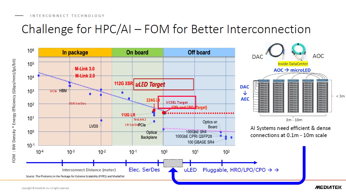
In high-performance computing (HPC) and artificial intelligence (AI) systems,interconnect performance is increasingly becoming a critical bottleneck, and theFigure of Merit (FOM)—defined as bandwidth density multiplied by energy efficiency—has emerged as a key metric for evaluating the suitability of different technologies across various interconnect distance scales.
Across distances ranging from a few micrometers to several meters, traditional electrical interconnects such asLVDSandSerDesmaintain relatively stable FOMs at short ranges. However, in the context ofAI data centers, where interconnect distances typically span0.1 m to 10 m, their FOMsdegrade significantly, failing to meet the growing demand for high-speed communication between densely packed compute units.
To address this challenge,MediaTekhas identified technologies such asMicroLED (uLED)andVCSELas promising candidates. These optoelectronic solutions demonstratesuperior FOM performance, particularly in the“off-board” range between 1 m and 10 m. Compared to traditional copper-based solutions likeDACsandAOCs, these emerging optical technologies offersubstantial improvements in both energy efficiency and bandwidth density, making them crucial enablers for overcoming interconnect limitations inScale-Up and Scale-Out architectures.
For MediaTek, establishing a differentiated competitive edge inAI chip platforms,intelligent edge computing, anddata center system architecturewill increasingly depend onsystem-level interconnect FOM. By strategically deploying technologies such asuLED, Silicon Photonics (SiPh), and Co-Packaged Optics (CPO)across varying distance and power domains, MediaTek can build a future-proof, high-efficiency interconnect foundation optimized for next-generation AI workloads.
MediaTek’s Optical Interconnect Roadmap: From Pluggable Optics to CPO
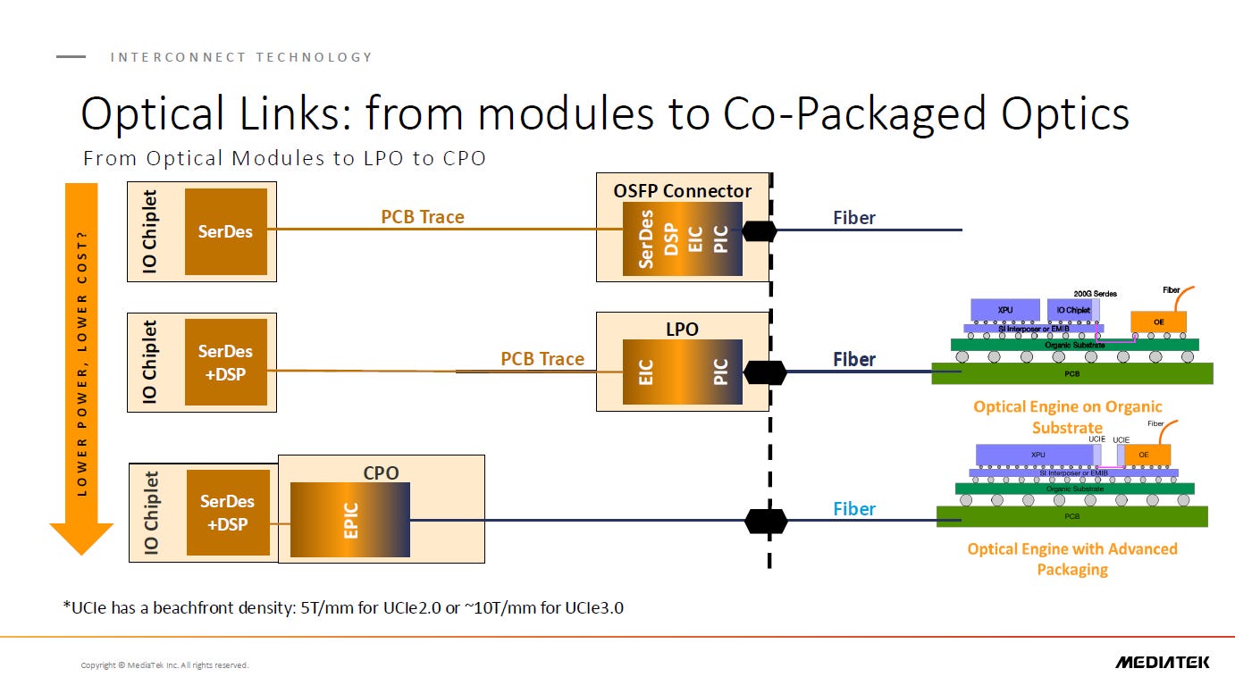
In this illustration,MediaTekoutlines the technological evolution fromconventional optical modulestoLinear Pluggable Optics (LPO)and ultimately towardCo-Packaged Optics (CPO). This trajectory reflects a clear trend in the data center and AI accelerator domains—optimizing power efficiency and cost at scale.
At the top layer of the stack, the traditional module architecture integratesSerDes and DSP, transmitting signals viaPCB tracesto an externalOSFP optical module. While this remains the current mainstream solution, it comes with relativelyhigher power consumption and packaging costs.
Moving forward,LPOimproves upon this by relocatingDSP functionality to the I/O chiplet or optical module, effectively reducing system power consumption. However, like the previous architecture, it still depends on PCB transmission between the chip and the pluggable optics.
At the most integrated level liesCPO, which co-packages theSerDes, DSP, and electro-photonic integrated circuits (EPIC)directly on the substrate, enablingdirect fiber coupling. This dramatically reduces the interconnect length,minimizes insertion loss, and enhancesenergy efficiency and form factor compactness. Moreover, this architecture is well-positioned to supportultra-high-density interconnects, such asUCIe, with bandwidth densities reaching5 Tbps/mm (UCIe 2.0)andup to 10 Tbps/mm (UCIe 3.0)—critical for future AI and HPC systems demanding low power and high scalability.
FromMediaTek’s perspective, these integrated optical interconnect technologies will be key to differentiating its offerings acrossdata center ASICs, XPU platforms, and edge AI inference modules. CPO and its associated technologies will enhance MediaTek’ssystem integration capabilities, especially as the industry converges toward architectures that fusecommunication and computationin the AI era.
The Transition from Traditional Electrical Interconnects to Co-Packaged Copper (CPC) for 400G Transmission
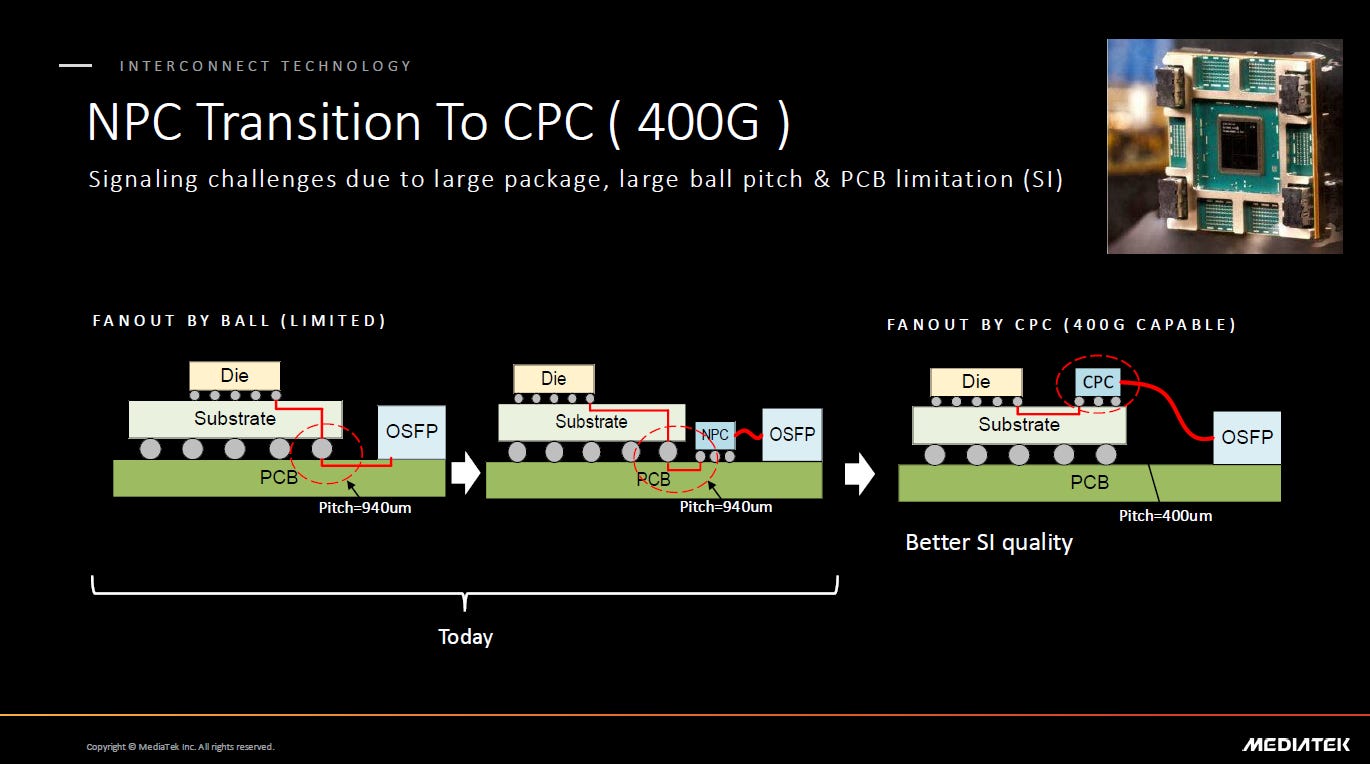
As data transmission rates advance toward400G and beyond, the limitations of traditionalfan-out by ballelectrical interconnects are becoming increasingly apparent. Current packaging methods are constrained byPCB trace losses,large ball pitch (typically 940 µm), and severesignal integrity (SI) degradation, which collectively hinder their ability to support high-bandwidth communication.
Although intermediate solutions such asNear Package Connectors (NPCs)have been introduced to mitigate these issues, they fail to fully address challenges related tosignal lossandhigh-frequency interference.
The adoption ofCo-Packaged Copper (CPC)addresses these challenges by bringinghigh-speed interconnect modules closer to the chip, integrating them directly within the package substrate. This approach significantlyreduces the interconnect path lengthand enables atighter ball pitch of around 400 µm, resulting insubstantial improvements in signal integrity and overall transmission quality.
This architectural shift is crucial for the evolution ofnext-generation AI and data center infrastructure, where ultra-high-speed interconnects are a fundamental requirement. For companies likeMediaTek, embracing packaging innovations such as CPC will be astrategic imperativeto establish long-term competitiveness inhigh-performance interconnects and data infrastructure platforms.
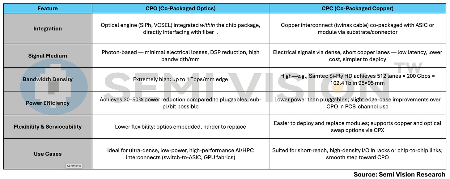
CPO vs CPC — Core Differences
CPC — Key Suppliers & Ecosystem Progress
Samtec: Leading Co-Packaged Copper connector innovator.
Si‑Fly HD CPC: Supports 200–224 Gbps PAM4 per lane, enabling 102.4 Tb in a 95×95 mm substrate region .
Broadcom + Samtec: Demonstrated a live 200 G CPC channel at DesignCon 2025 (Si‑Fly HD + Broadcom 200 G SerDes) with reliable BER performance over 30 mm substrate + 150 mm cable .
Luxshare‑Tech: Actively showcasing CPC for 224/448 Gbps, positioning CPC as transitional to CPO; embedded in top data center supply chains
TE Connectivity: Developed co-packaged socket technologies supporting separable copper/optical modules with 0.40 mm pitch, enabling near-package integration .
Amphenol, Molex, etc.: Engagement in co-packaged copper connectors, near-chip cable assemblies (e.g., OSFP), and PCIe 7.0 support
Choosing the Right Path
CPCoffers anincremental, lower-cost pathwith simplified integration and serviceability, ideal for short-reach, high-density interconnects (e.g., within racks or chip-to-chip).
CPOdelivers theultimate performance leapin bandwidth and power efficiency, targeting long-term AI/HPC visions, despite higher integration complexity and thermal demands.
Hybrid / Transitional strategy(e.g., CPX connectors) supports modular swapping between copper and optics, easing deployment challenges .
For MediaTek, embracingCPC as a near-term solutionwhile strategically investing inCPO readinessaligns with building high-performance, scalable AI infrastructure across chip, package, and data center levels.

Integrating Electrical and Optical Subsystems in XPU/AI Architectures: Challenges and Strategic Implications
In XPU and AI computing systems, the coexistence of electrical and optical interconnect subsystems introduces a complex set of trade-offs. When data transmission rates remain below400 Gbps,copper-based electrical interconnects—such as those usingSerDesandNear Package Connectors (NPCs)—continue to dominate. However, these traditional solutions are increasingly strained bysignal integrity (SI)issues as frequencies rise.
Once transmission speeds surpass400 Gbps, transitioning toCo-Packaged Copper (CPC)architectures helps alleviate SI concerns by reducing path lengths and improving impedance control. Yet, this shift also introduces new levels ofpackaging and manufacturing complexity, particularly in high-density system designs.
Amid these challenges, theoptical engineis emerging as a critical enabler to overcome interconnect bottlenecks—especially withinAI accelerator (XPU) architectures, where it now stands alongsideHBM memory,PCIe, andEthernetas a core subsystem. By adoptingCo-Packaged Optics (CPO), designers can achieveon-package electro-optical integration, enabling significantly higher bandwidth and lower power consumption.
However, this advancement raises the bar across multiple fronts, requiringtight integration of optical packaging, thermal management, and high-precision manufacturing. ForMediaTek, building a competitive XPU platform for AI and high-speed interconnect applications will demand a strategic focus onoptical engine development, CPO packaging, and system-level co-design capabilities. These elements will be essential to unlocking scalable, energy-efficient performance in next-generation AI infrastructure.
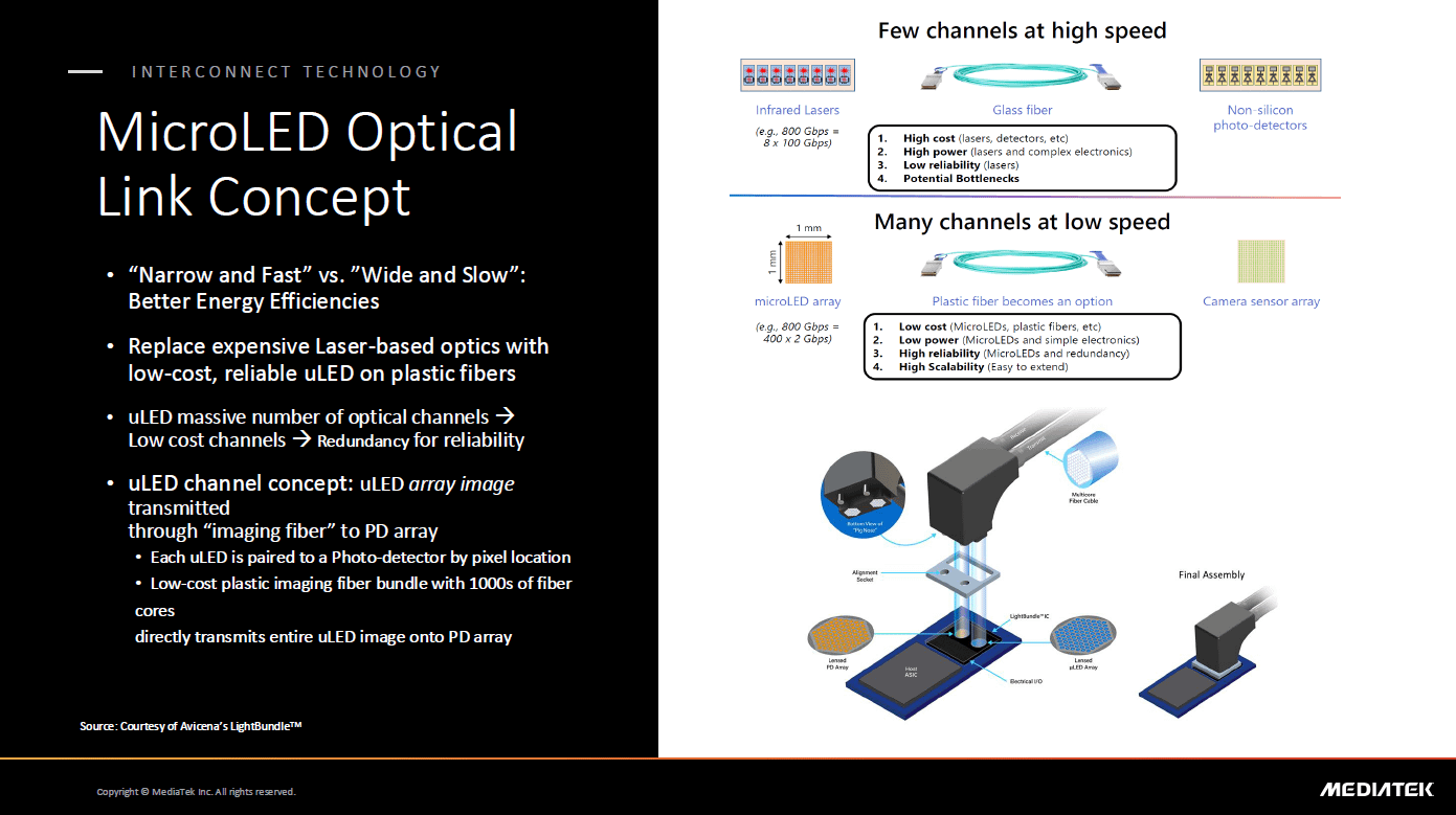
MicroLED Optical Links: A Scalable, Low-Cost Alternative to Traditional Laser-Based Interconnects
TheMicroLED (uLED)optical link represents an innovative alternative to traditional high-cost laser-based optical modules. Conventional optical communication architectures typically rely on a small number ofhigh-speed channels(e.g., 8 × 100 Gbps), requiring expensive laser sources, glass fibers, and non-silicon photodetectors. This results in high system costs, elevated power consumption, limited reliability, and ultimately, bandwidth bottlenecks.
In contrast, theuLED-based architectureembraces a “wide and slow” strategy by leveraginga large number of low-speed optical channels. By combining denseuLED arrayswithplastic optical fibers, the system significantly reduces bothcost and power consumption, while the inherentredundancyof the architecture improves reliability and scalability.
In this design, each uLED pixel corresponds to a dedicated photodetector (PD), and the light is transmitted via animaging fiber, effectively transferring the optical “image” of the uLED array directly to the PD array. This novel structuresimplifies the optical pathand reduces component complexity, making it highly promising forshort-range, high-bandwidth, low-latency interconnectsin AI and HPC data center environments.
ForMediaTek, adoptinguLED-based optical linkspresents a strategic opportunity toredefine the foundation of mid- to short-range high-speed connectivity, especially in applications that demandlow power and high integration density. As AI workloads scale, uLEDs could enable a new class of cost-efficient, energy-aware optical interconnects, positioning MediaTek at the forefront of next-generation data infrastructure innovation.
Interconnect Innovation at the Core of AI and Cloud Data Center Performance
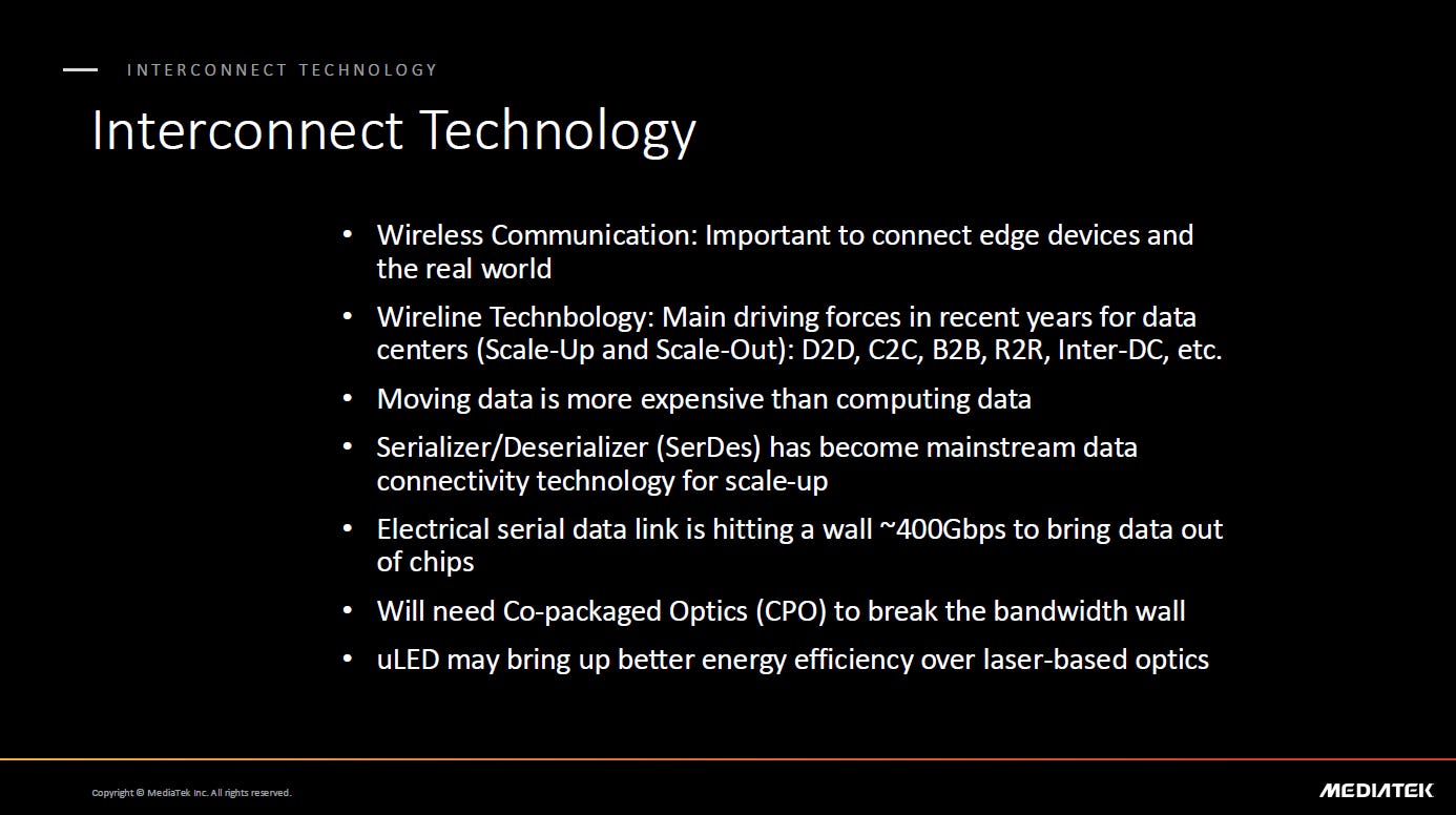
In the evolving architecture of AI- and cloud-driven data centers,interconnect technologyhas emerged as a critical enabler for breaking through system performance bottlenecks. Whilewireless communicationplays a vital role in connecting end-user devices to the physical world,wired interconnectsremain the driving force in high-density computing environments. These span across a hierarchy of transmission scenarios—includingDie-to-Die,Chip-to-Chip,Board-to-Board,Rack-to-Rack, andData Center-to-Data Centerlinks.
As AI models scale rapidly,data movement costs now outweigh computation itself, imposing severe constraints on bothperformance and energy efficiency.SerDes (Serializer/Deserializer)technology has become the mainstream solution for data links, but thebandwidth limit of electrical channels caps out around 400 Gbps, falling short of the increasing I/O demands of next-generation systems.
To overcome this “bandwidth wall,” the industry is shifting towardCo-Packaged Optics (CPO)—a transformative approach that integrates optical engines directly within the package to reduce power and latency. Notably,MicroLED (uLED)technology is gaining attention as apotential low-power alternative to traditional laser-based optical modules, offering a morecost-effective and reliable solutionfor future optical interconnects.
These advancements are reshaping not onlychip design and packaging strategies, but also thefundamental fabric of data center interconnect infrastructure, laying the groundwork for scalable, energy-efficient AI computation.
MediaTek’s Latest Developments in Optical Interconnects and Co-Packaged Optics (CPO) for AI/HPC Systems
- Optical Interconnect Integration and Co-Packaged Optics (CPO) in AI/HPC Chips
MediaTek has showcased a live demonstration of a6.4 Tbps Co-Packaged Optics (CPO)solution developed in collaboration withRanovus, integrating high-speed optical engines directly into ASIC chips to enhance bandwidth and efficiency in data centers.
With the exponential growth inAI trainingandhigh-performance computing (HPC)demands, traditional electrical interconnects are hitting bandwidth and energy-efficiency bottlenecks. In response, MediaTek has begun incorporatingoptical interconnect technologyinto its custom AI/HPC chip designs. Through CPO, optical engines are integrated directly within the chip package, eliminating the need for external optical modules and reducing signal path length.
In 2024, MediaTek launched a next-generation ASIC design platform combining its in-house112 Gbps long-reach SerDeswithRanovus’ Odin® optical engine, forming aheterogeneously integrated electro-optical I/O interface. The design supportseight 800 Gbps electrical linksandeight 800 Gbps optical linksvia a modular, pluggable interface, enabling flexible deployment to meet varying system needs. This architecture offers aversatile, high-speed connectivity solutiontailored for AI/HPC chip platforms.
MediaTek’s approach uses112G SerDes signals to directly drive the optical engine, as opposed to more complex integrated silicon photonics solutions. This results in areduced PCB footprint,lower BOM cost, and up to50% reduction in system power consumption.
From a competitiveness standpoint, MediaTek leverages itsadvanced 3nm process,2.5D/3D packaging capabilities, and deep experience inhigh-speed interface design and thermal managementto deliver a CPO-enabled chip that meets world-class standards in performance and efficiency. Compared to industry leaders such asNVIDIAandBroadcom, which have already deployed CPO switch chips, MediaTek’s solution offersmodular pluggabilityandhybrid integration of electrical and optical signals—positioning it as a promising contender in the next-generation AI/HPC interconnect market.
- Collaborative Ecosystem and Strategic Positioning in Optical Interconnects
In the development of optical interconnect technologies,MediaTekhas actively adopted acollaborative ecosystem strategy, working closely with partners across foundry, materials, packaging, and optical component supply chains to accelerate innovation and deployment.
At theprocess and advanced packaging level, MediaTek relies onTSMCnot only for cutting-edge logic process nodes but also as a critical enabler for CPO chip packaging.TSMC’s silicon photonics platformand itsCOUPE heterogeneous integration frameworkallow for the combination of65nm photonic dies with advanced logic chips, and throughSoIC-X and CoWoStechnologies, enable3D-stacked optical modulessuitable for CPO implementations. MediaTek collaborates closely with TSMC to leverage these capabilities for high-yield production of optical interconnect chips.
On theoptical source and device front, MediaTek is exploring innovations from startups likeAvicena, which specializes inLightBundle™ technologybased onGaN MicroLED arrays. This approach replaces traditional laser-based sources with ultra-low-power, massively parallel optical links. Recently, TSMC announced a partnership with Avicena to co-developmicroLED transmitters and photodetectors, aiming to improve energy efficiency in AI data transport. This partnership signals a strong ecosystem convergence betweenfoundry leadership and photonics innovation, and positions MediaTek to potentially incorporateAvicena’s sub-1 pJ/bit interconnect technologyinto its future AI/HPC platforms—dramatically reducing inter-chip power consumption compared to conventional CPO (~5 pJ/bit).
On thematerials and module level, Taiwanese suppliers such asElite Material Co. (EMC)andITEQprovidehigh-frequency copper-clad laminates (CCLs)andsubstrate technologiesfor optical modules. These companies are scaling production to meet growing AI server demand, introducingM6, M7, and M8-gradematerials already adopted by leading AI GPU and ASIC vendors. Through collaboration with local material partners, MediaTek ensures its CPO modules and optical packaging solutions meet stringenthigh-speed, low-loss electrical performance requirements.
In parallel, MediaTek is working closely with majorOSAT (Outsourced Semiconductor Assembly and Test)partners such asASE, which is developingCPO-specific testing interfaces and assembly workflowsto support next-generation packaging requirements.
Overall,MediaTek’s optical interconnect strategy is built on vertically integrated collaboration:
Upstream, it leveragesTSMC’s advanced logic and packaging platforms(e.g., InFO, CoWoS, SoIC);
Midstream, it integratesoptical engine innovationsfrom startups such asRanovus and Avicena;
Downstream, it co-developsmaterials and packaging solutionswithTaiwan’s substrate and module suppliers.
This end-to-end approach allows MediaTek to build acomprehensive and scalable optical interconnect ecosystem, enabling high-efficiency, high-bandwidth connectivity for future AI and HPC systems.
- R&D Investment in microLED and Optical Engine-Based Transmission Solutions
MediaTek is actively exploringmicroLED (μLED)andnext-generation optical engine technologiesas potential solutions forhigh-speed, low-power optical data transmission. microLEDs—thanks to their small footprint, high modulation speeds, and compatibility with CMOS processes—can be fabricated intodense arrays for massively parallel optical communications, offering higher bandwidth density and lower power consumption compared to traditional copper-based links.
Industry observers increasingly viewmicroLEDs as a viable alternative to copper interconnects for short-reach (sub-10m)applications, providing energy-efficient, high-speed data transfer. For example, Taiwan-based LED leaderEnnostaris actively developing integrated solutions that combineMicro LED, VCSEL, and InP lasersfor AI-centric optical communications.
For MediaTek,microLED-based optical enginesrepresent a promising option forinter-chip optical busesorintra-package optical interconnectsin multi-chip systems. In theLightBundle™ architecturepioneered byAvicena, hundreds ofblue microLEDsact as light sources, transmitting images throughimaging fiberto align with silicon photodetector arrays at the receiver end. This setup enables point-to-point, massively parallel optical links. Unlike conventional laser-based systems that rely on high-speed external modulators, each μLED pixel directly modulates individual data streams—simplifying the system architecture while reducing cost and power consumption.
This architecture has recently seen tangible progress:Avicena and ams OSRAMhave begunvolume production of GaN microLED arrays, andAvicena is collaborating with TSMCto co-optimize integrated silicon photodetectors. MediaTek envisions using this class ofμLED optical enginesto lowerchip-to-chip interconnect power consumption to under 1 pJ/bit, significantly outperforming today’s mainstream CPO solutions (~5 pJ/bit).
Beyond μLEDs, MediaTek is already leveragingoptical engine technologiesin its current CPO implementations. Notably, the company has partnered withRanovusto deploy theOdin® optical engine, a cutting-edge CPO solution. Odin utilizes amonolithic electro-optical architectureintegrating drivers, transimpedance amplifiers, silicon photonic modulators, and photodetectors on a single chip. It supportsdirectly driven 100 Gbps wavelengths, along with external passive fiber and laser integration. The6.4 Tbps CPO 3.0 Odin enginedeliversindustry-leading energy efficiency at 4 pJ/bit (including laser)and featuresthe highest-density 100G optical I/O, cuttingsystem power, footprint, and costby half.
This co-developed CPO optical engine was showcased atOFC 2024, demonstratingMediaTek’s ability to rapidly integrate innovative optical engines into its ASIC platforms. Moving forward, MediaTek plans to continue tracking the advancement ofsilicon photonics, VCSEL arrays, μLEDs, and other optoelectronic transmission technologies, evaluating their potential integration into future AI/HPC architectures.
In the near term, MediaTek will focus optical engine deployments oncloud data center chips, such asswitch ASICs and AI accelerators, targeting high-speed I/O applications. In the longer term, MediaTek mayextend compact optical engine technologies into high-end networking equipment, PCs, and servers, aiming to overcome electrical bandwidth limitations while delivering energy efficiency advantages.
- Technical Strategies and AI xPU Platform Development to Address Scale-Up/Scale-Out Demands in AI Data Centers
To address the immense bandwidth and energy-efficiency challenges associated with bothScale-UpandScale-Outarchitectures in AI data centers,MediaTekis deploying a portfolio of cutting-edge technologies—includingSerDes, Co-Packaged Optics (CPO), Linear Pluggable Optics (LPO), and microLED (μLED)—to overcome the “bandwidth wall” and power bottlenecks, while shaping its roadmap forAI computing platforms (xPU).
For Scale-Up architectures, which require high-speed communication within AI superchips or multi-die modules, MediaTek has developed advancedSerDes (Serializer/Deserializer)technologies. According to official disclosures, MediaTek has launched224 Gbps SerDes IP, a leading-edge solution used in interfaces such asPCIe 6.0, memory channels, andchip-to-chip buses, enabling customers to increase throughput and reduce total cost of ownership (TCO). Looking ahead, MediaTek is also investing in the development ofnext-generation 448 Gbps SerDesto meet the escalating communication bandwidth demands of future AI chips.
In addition,MediaTek has joined NVIDIA’s NVLink-C2C/NVLink Fusion ecosystem, supporting high-bandwidth interconnects between its ASICs and NVIDIA GPUs. This enables flexible heterogeneous acceleration modules and allows MediaTek ASICs to be directly linked with NVIDIA GPUs for more efficient Scale-Up compute architectures.
For Scale-Out deployments, MediaTek emphasizes two key optical interconnect technologies:CPO and LPO.
CPOintegrates optical transceivers directly into the same package as switch or accelerator chips, minimizing the distance between electrical and optical domains. This enablesmulti-terabit per second board-level bandwidthwhile reducingper-bit power consumption by up to 50%, resolving signal loss and latency issues associated with traditional pluggable optical modules and PCB traces.
LPO (Linear-drive Pluggable Optics)serves as a middle-ground solution between traditional DSP-based optics and CPO. In LPO designs, the DSP and driver ICs are eliminated from the optical module; instead, the main chip directly linearly drives the optical components, retaining only high-linearity amplifiers and drivers. This significantly reducespower consumption and latency, while maintaining theserviceability benefits of pluggable modules.
MediaTek’s data center interconnect strategy is expected to combineCPO and LPO:
CPOis prioritized forshort-reach, high-bandwidth density links, such as between AI accelerators and switches;
LPOis suited forrack-to-rack mid-range links, enabling energy-efficient optical transmission over several meters.
OnceμLED-based interconnect technologiesmature, MediaTek may also integrate them intoultra-short-reach chip-to-chip (C2C)interconnects, further reducing interconnect power toas low as 1 pJ/bit.
On a system level, MediaTek is building its ownAI compute platform portfolio (AI xPU). On one hand, it targets thecustom AI ASIC marketfor cloud-scale applications, leveraging itsSerDes, advanced process nodes, and packaging expertiseto deliver high-performance data center chips. For example, MediaTek has collaborated withNVIDIA on the “GB10 Superchip”, a fused architecture combining theGrace CPUandBlackwell GPU, delivering over1,000 TOPSand supporting200B+ parameter AI models locally. This underscores MediaTek’s growing role in cutting-edge AI chip design.
On the other hand,MediaTek is developing its own line of AI accelerators, with Chairman Ming-Kai Tsai confirming that the company is working on next-generation chips using3nm and 2nm process nodes, potentially integratingArm Neoverse IPfor data center-class performance. These chips are expected to enter production and contribute to revenuepost-2025, with MediaTek forecasting theAI accelerator market to reach $45 billion by 2028.
In summary, MediaTek is building a vertically integrated architecture across AI workloads—fromin-package interconnects (SerDes/NVLink), board-level and rack-level optical links (CPO/LPO), to future μLED-based chip-to-chip connections—to construct scalable, high-efficiencyAI xPU solutionscapable of powering the next era of large-scale AI computation.
- Technology Optimization for Edge AI Devices: Voice Assistants, Smart Home Hubs, and AI Tablets
MediaTek is actively extending its portfolio of advanced interconnect and AI technologies intoEdge AI devices, includingvoice assistants,smart home hubs, andAI-enabled tablets. The company focuses on optimizingpower consumption, cost-efficiency, and system-level integrationto meet the unique constraints of these endpoints.
MediaTek addresses this need throughhighly integrated System-on-Chip (SoC) designsthat combine CPUs, GPUs, NPUs (Neural Processing Units), DSPs, memory controllers, andconnectivity modules (Wi-Fi, Bluetooth, 5G)into asingle-chip solution. This integration eliminates the need for multi-chip interconnects, reducing both power consumption and bill-of-materials (BOM) cost. The SoCs are fabricated usingadvanced process nodes (e.g., TSMC 4nm/3nm)and are equipped with MediaTek’s proprietaryNeuroPilot AI engine, capable of executing sophisticated inference workloads such asautomatic speech recognition (ASR)andcomputer visionwithin tight power budgets.
Power efficiency is further enhanced throughfine-tuned power management and ultra-low power standby modes, tailored for devices like voice assistants that must remain active for extended periods while consuming minimal energy. For example, MediaTek’s flagshipDimensity 9400mobile SoC—designed for premium smartphones—has also been adapted forAI smart home hubs, leveraging its compute performance and AI inference capabilities.
AtCES 2025, MediaTek andEtron Technologyshowcased aSmart Home AI Hubbased on theDimensity 9400 platform, integrating Etron’s ASR AI technology with MediaTek’sAgentic AI engine. The platform enableslocal executionof tasks such assmall language model (SLM) inferenceandmulti-modal AI processing, empowering personalized and responsive voice assistant experiences without relying solely on the cloud. Thison-device AI processingnot only reduces latency but also significantly cuts bandwidth costs associated with cloud inference.
MediaTek’sAgentic AI enginefurther enhances terminal AI functionality by enablingautonomous reasoning and contextual learning, allowing edge devices to adapt to user preferences over time and act proactively.
In addition to AI compute,connectivity remains a core strength for MediaTek. The company leads inWi-Fi 6/6E/7,Bluetooth Low Energy, and5G NTN (Non-Terrestrial Network) satellite communication. In the smart home context, this allows devices to seamlessly connect tosensors, appliances, and cloud services, forming a cohesiveAIoT (AI + IoT)ecosystem. For example, MediaTek’s SoCs already supportlow-Earth-orbit (LEO) satellite communication, enabling future voice assistants to access AI services even in the absence of terrestrial networks.
In essence, MediaTek is adapting itsdata center-class technologies to the edge, balancingintegration, energy efficiency, and intelligence:
SoC integrationreduces cost and power draw;
Advanced packagingsupports optional memory stacking or heterogeneous components;
AI IP blocks and optimized software stacksenhance local inference performance;
Strong connectivity frameworksensure fluid Edge-Cloud collaboration.
- Advanced Packaging Strategies (CoWoS, EMIB, SoIC) and Their Role in Optical Interconnects and CPO Deployment

Advanced packaging has become a cornerstone of MediaTek’s strategy to enable high-density integration and optical interconnects for next-generation HPC and AI platforms. Leveraging TSMC’s portfolio of 2.5D and 3D packaging technologies, including CoWoS, InFO, and SoIC, MediaTek has built comprehensive capabilities that span chiplet integration, high-speed I/O, and vertical die stacking.

CoWoS (Chip-on-Wafer-on-Substrate)is a 2.5D silicon interposer-based packaging technology developed by TSMC. It allows multiple chips—such as logic dies andHigh Bandwidth Memory (HBM)—to be placed side by side on a silicon interposer. MediaTek has adopted CoWoS in its custom ASIC designs to meet the high memory bandwidth and low-latency access demands of modern data centers. In its high-performance AI chips, MediaTek offers support for CoWoS, InFO, and hybrid CoWoS architectures to address the specific requirements of hyperscale clients.

SoIC (System on Integrated Chips)represents TSMC’strue 3D stacking solution, enabling direct wafer-to-wafer or die-to-wafer hybrid bonding. MediaTek has developed in-house capabilities for 3D heterogeneous integration, allowing vertical stacking of dissimilar dies to form3.5D architectures. This is particularly relevant forCo-Packaged Optics (CPO), where photonic dies can be vertically integrated atop logic ASICs using SoIC, significantly reducing electrical-optical path lengths and boosting bandwidth density. TSMC’sSoIC-Xcombined with CoWoS has already been demonstrated as a scalable platform for CPO module integration, and MediaTek is positioned as one of thefirst adoptersof this hybrid packaging approach.
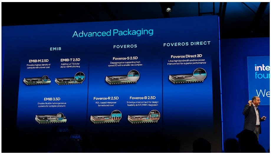
On theIntel side,EMIB (Embedded Multi-Die Interconnect Bridge)offers a silicon bridge embedded within the package substrate to connect chiplets, providing high-speed, localized interconnect without requiring a full-size silicon interposer. Compared to traditional interposer-based packaging, EMIB reduces cost and simplifies manufacturing. While MediaTek primarily uses TSMC’s packaging ecosystem, its ongoing collaboration with Intel Foundry Services (e.g., for 16nm IoT SoCs) opens the possibility of adoptingIntel’s EMIB or Foveros 3D stacking technologiesin select product lines.

2025年5月1日
Overall, MediaTek is building an end-to-end integration platform aroundchiplet architectures, high-speed SerDes interfaces, and advanced packaging. Within its latest AI/HPC ASIC roadmap, MediaTek highlights its capabilities in:
224 Gbps SerDes IP
TSMC’s leading-edge nodes
CoWoS and SoIC-based 2.5D/3D designs
Customized HBM integration and interposer co-design

Moreover, MediaTek is an early member of theNVIDIA NVLink Fusion ecosystem, enabling it to participate in high-bandwidth, low-latency interconnects for heterogeneous compute systems.

These packaging technologies directly empower MediaTek’s optical I/O and CPO strategies:
CoWoSallows close physical integration of theRanovus Odin® optical enginenext to ASICs, ensuring high-speed electrical-optical transitions.
SoIC stackingopens the door for vertically integrating photonic dies directly on top of logic SoCs, minimizing interconnect length, increasing optical port density, and optimizing power efficiency.
MediaTek is expected to continue embedding advanced packaging into its products across tiers. Formobile and consumer applications, vertical stacking can enhance performance-per-watt ratios in compact form factors (e.g., AI tablets and hybrid AI clients). Forcloud-scale AI accelerators, combining CoWoS with SoIC enables ultra-wide bandwidth communication channels and massive HBM bandwidth integration.
Looking ahead to the2nm era, MediaTek has already announced its plan to adoptTSMC’s N2 nodewith integrated advanced packaging. The goal is to deliver15% performance uplift and 25% power reduction, providing a robust foundation for its future AI and edge-cloud compute platforms.
In summary, MediaTek’s comprehensive packaging strategy—spanning2.5D (CoWoS, EMIB), 3D (SoIC), and hybrid 3.5Dintegration—forms the backbone of its optical interconnect and CPO ambitions. By tightly coupling photonics, memory, and high-speed I/O through advanced packaging, MediaTek is poised to deliver scalable, energy-efficient, and bandwidth-rich compute platforms tailored for the AI era. This approach not only strengthens MediaTek’s competitiveness in next-gen HPC/AI chips but also underscoresTaiwan’s leadership in the convergence of advanced packaging and optical interconnect ecosystems.


PreviousNext
TopLatestDiscussions








See all