Beyond TIM: Microchannel Architectures for Advanced Thermal Management
Beyond TIM: Microchannel Architectures for Advanced Thermal Management
- Source: SemiVision
- Author: SEMIVISION
- Published: 2025-07-22T18:45:16+08:00
- URL: https://tspasemiconductor.substack.com/p/beyond-tim-microchannel-architectures Beyond TIM: Microchannel Architectures for Advanced Thermal Management


Beyond TIM: Microchannel Architectures for Advanced Thermal Management
Original Articles By SemiVision Research (IEEE ECTC , KLA , EVGroup , Meta , TSMC ,HP , Google , ASE , SEMI )

Jul 22, 2025
∙ Paid
In our previous discussions, we explored how MEMS technology can be leveraged to address thermal management challenges through the implementation of microchannel cooling. Building upon that foundation, this article delves into the fabrication of microchannels using MEMS-based semiconductor processes. We will further examine how bonding technologies—such as wafer-to-wafer (W2W) or die-to-wafer (D2W) bonding—enable the integration of device wafers, HBM (High Bandwidth Memory) wafers, and embedded microchannel structures. Through this analysis, we aim to illustrate how these advanced techniques can enable next-generation 3D-stacked architectures with enhanced thermal efficiency.

2025年7月13日

2025年7月11日

2025年7月9日
In the era of AI and high-performance computing (HPC), chip design is pushing the limits of power density and thermal load. As a result, thermal management has become the foremost concern in chip development. This is not merely a system-level engineering issue—it is a comprehensive challenge spanning chip architecture, process design, packaging, and system integration. In AI chips, we are not only dealing with extreme computational intensity but also facing a fundamental physical constraint:there are only three ways to transfer heat—conduction, convection, and radiation.
To begin with, modern AI chips are inherently “hot” designs—power densities often exceed hundreds of watts per square centimeter. These levels far surpass the capabilities of conventional server cooling techniques, making advanced cooling solutions such as cold plates and microchannel cooling essential.
However, despite the high power demands, our options for heat transfer remain limited.Thermal radiationis practically ineffective at room temperature—it increases with the fourth power of temperature (T⁴), and at standard operating conditions, its contribution to heat dissipation is negligible. Therefore, onlythermal conductionandthermal convectionare realistically viable for cooling AI chips.
Thermal conductiongoverns how heat is extracted from within the chip. This heat path involves: the silicon substrate itself, metal interconnects, TIM1 (typically made of indium or graphite), the package lid, then TIM2 (such as graphite sheets or thin thermal pastes), and finally the heatsink or cold plate. Each layer’s thickness and thermal conductivity determines the efficiency of heat flow. For instance, TIM1 may be 100 microns thick, while TIM2 can be as thin as 1 micron—this design difference reflects the need to minimize thermal resistance (TR) and temperature gradients.
Thermal convection, on the other hand, deals with how quickly that heat is removed once it exits the chip package. From conventional fans and air cooling, to advanced cold plates and liquid cooling loops, to next-generation microchannel-based liquid cooling, system-level convection mechanisms have become essential to AI server infrastructure.
Within this framework,foundries and assembly houses must collaborate closely in thermal design. Traditionally, wafer fabrication and packaging were treated as separate domains, with boundaries defined by I/O and mechanical interfaces. But in the high-heat AI chip era, thermal design must transcend these boundaries. Wafer design must include provisions for thermal vias (TSVs) or copper pillars, backside trenches, and thermal spreaders. On the packaging side, one must integrate high-performance TIMs, optimized lid structures, microfluidic cold plates, and reliable fluidic interfaces. Packaging is no longer just about protection and I/O—it has become a core thermal management component.
This becomes even more critical with the increasing adoption ofsilicon photonics, which is highly temperature-sensitive. Minor thermal fluctuations—just a few tens of degrees—can cause optical drift, coupling losses, or complete failure. Traditional thermal design approaches are insufficient to meet these demands, requiring more proactive, localized, and fast-responding cooling strategies.
In summary, thermal design for AI chips is no longer a secondary step in the engineering flow. It is a multi-layered, interdisciplinary challenge that begins with architectural planning and extends all the way to system integration. Since heat can only be managed through conduction and convection, effective removal of thermal energy from the chip’s core demands synchronized efforts between foundry and assembly teams—across materials, layouts, interfaces, and manufacturing technologies. This is not only a physical necessity, but also a fundamental shift in system design philosophy.

The core challenge in AI chip thermal management today lies squarely within the chip itself. Therefore, it is crucial for foundries to propose systematic solutions from their end of the value chain. The following details further elaborate on this point, with a focus on TSMC’s efforts under silicon-based architectures—specifically in the exploration of microchannel cooling, DRIE/MEMS applications, copper pillar array design, TIM material challenges, and No-TIM architectures. These thermal solutions are applicable not only to SoW and CoWoS but also to silicon photonics-integrated advanced packaging.

2025年6月13日

2025年6月2日

2025年6月27日
Foundry Perspective: Why Chip Thermal Architecture Must Be Led by the Foundry Side
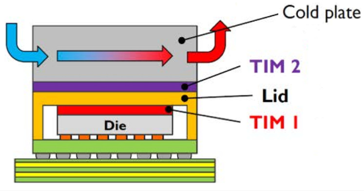
Source: Xidian University, Xi’an
The classical AI chip thermal stack typically follows this structure:
AI Chip → TIM1 → Lid → TIM2 → Cold Plate.
Within this heat dissipation path, multiple interface layers and material-related imperfections—such as voids or poor adhesion—contribute to increased thermal resistance, ultimately limiting the chip’s thermal budget and overall performance.
From the foundry's vantage point, the early stages of wafer fabrication and packaging provide a unique opportunity to define and control the heat flow path at the chip level. By initiating the design of the thermal architecture at the source, the foundry can not only improve thermal efficiency but also prevent integration challenges that may arise in later stages of advanced packaging.
This upstream integration enables:
Optimized Heat Spreading Paths:Direct engineering of silicon and interposer layers (e.g., using microchannels or embedded heat spreaders).
Material System Co-Optimization:Early-stage selection and integration of TIM materials or No-TIM alternatives that align with silicon process constraints.
Advanced 3D/heterogeneous compatibility:Ensuring that the thermal strategy scales effectively with 2.5D, 3DIC, and chiplet architectures, where vertical and lateral heat dissipation become even more critical.
As AI chips push toward higher power densities and tighter thermal margins, it is no longer viable to treat thermal design as a post-fabrication packaging problem. A foundry-led, co-optimized thermal strategy is now a prerequisite for high-performance and reliable AI silicon.
Microchannel Liquid Cooling Concept
In its IEEE ECTC papers and follow-up discussions, TSMC introduced the concept ofDirect Water Cooling (DWC)by etching microchannels directly into the backside of active dies using MEMS/DRIE processes. These microchannels are then integrated with CoWoS packaging and the interposer to form a unified cooling path. The cooling solution is capable of handling heat fluxes up to2.6 kW, with temperature differentials controlled within approximately63 °C.
TSMC explored various microchannel structures, includingtrench,pillar array, andplanar channeldesigns, with thepillar-based microchannelconfiguration demonstrating the best thermal performance.

2025年7月3日
MEMS/DRIE Process and Silicon Stress Management
Microchannels are fabricated at the wafer level using DRIE (Deep Reactive Ion Etching) to create TSVs or trench structures—commonly applied to silicon-based wafers. This process enables highly precise, high-aspect-ratio etching and is suitable for batch fabrication, making it ideal for microfluidic and thermal management applications in advanced packaging.
However, DRIE introduces mechanical challenges such as vertex stress (excessive stress at corners), wafer warpage, and increased risk of cracking or breakage during subsequent processing.
To mitigate these risks, foundries must implement stress relief structures and carefully manage trench pitch and aspect ratios, ensuring that the silicon microchannel structures remain stable and reliable under extreme thermal conditions and repeated liquid cooling cycles.
What is DRIE (Bosch Process)?
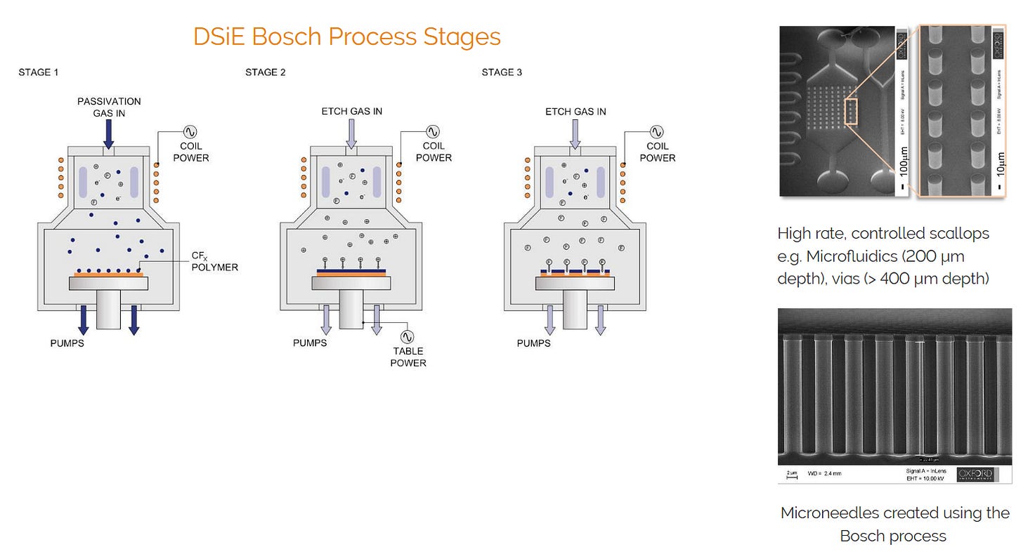
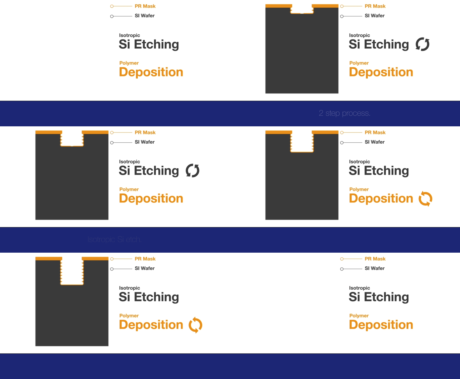
DRIE is a microfabrication technique used to etch deep and narrow features into silicon wafers with high precision. It is a key process in MEMS (Micro-Electro-Mechanical Systems) manufacturing and is particularly suited for creating microchannels, vias, and cavities with vertical sidewalls. The process alternates between etching and passivation steps to achieve high aspect ratios while maintaining structural integrity.
Copper Pillar Array for Enhanced Thermal Convection Paths
In addition to microchannels, TSMC has introduced theCopper Pillar Arrayas a supplementary structure to strengthen thermal convection pathways. These copper pillars can serve asmicro-bumpsorthermal columns, conducting heat directly from the active silicon layer and providing an additional solid-state thermal transfer path.
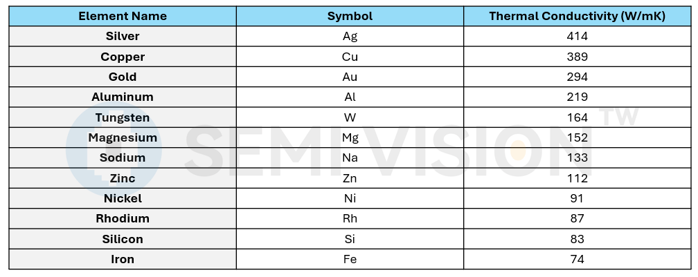
Copper, with its significantly higher thermal conductivity compared to TIM powders or phase-change interface materials, helpsreduce local thermal resistance. When tightly integrated with the cooling fluid pathways, the copper pillar array significantly enhancessystem-level thermal dissipation efficiency.
TIM Material Research vs. No-TIM Architecture Innovation
TIM Material Challenges: Voids, Adhesion, and Reliability
Common issues with TIM1/TIM2 layers include:
Interface Voids: These reduce thermal connectivity and increase thermal resistance.
Poor Adhesion: Leads to delamination between layers.
Material Degradation: High temperatures can cause material failure andpump-out, where TIM is displaced over time.
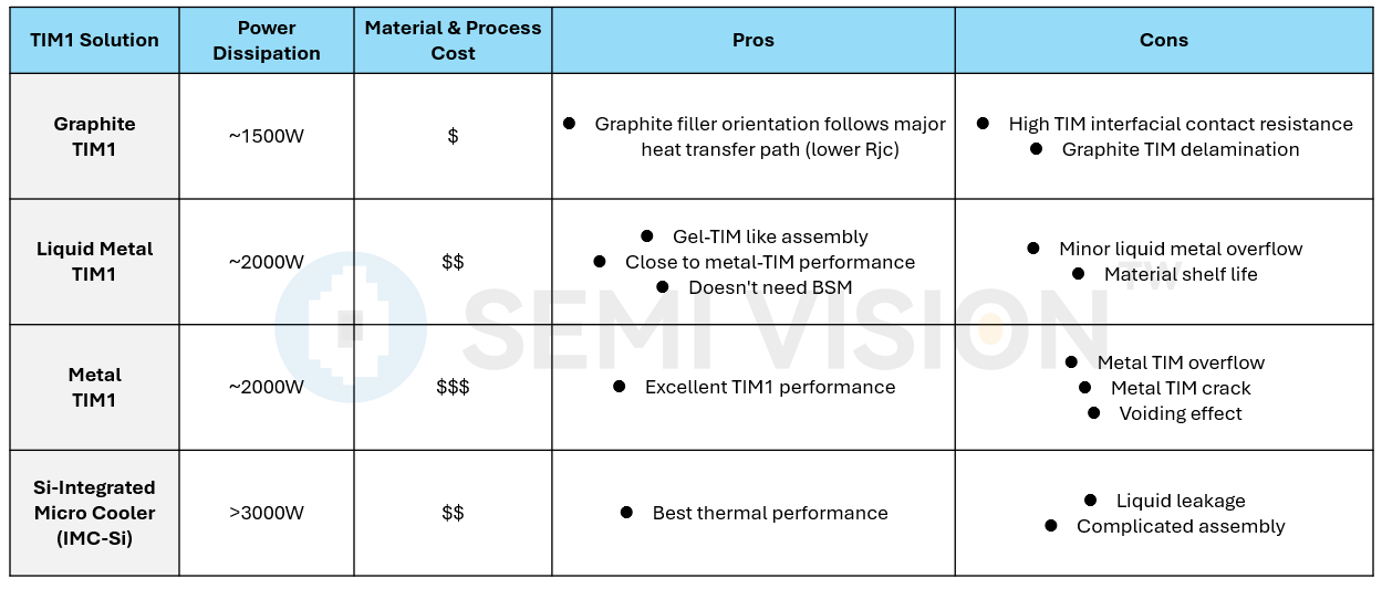
Indium alloy TIMs (≈80 W/m·K) offer excellent thermal conductivity but require surface metallization (e.g., Ti/Au or Ni/Au) on the chip backside and lid, along with areflow processto ensure low interfacial thermal resistance and high reliability.
No-TIM Architecture: A Breakthrough Innovation
TSMC has explored aDirect Water Cooling (DWC)architecture that eliminates the need for intermediate TIM layers. In this approach, microfluidic cooling channels are etched directly into the silicon die, enablingdirect contactbetween the cooling fluid and the heat-generating active layer. This significantly reduces interfacial thermal resistance.
In comparative tests across three architectures:
Pure DWC Architecture: Achieved2.6 kW heat loadwith aΔT of 63 °C— the best performance.
Oxide (OX) TIM Architecture: Reached2.3 kW / 83 °C.
Liquid Metal TIM Architecture: Handled around1.8 kW / 75 °C.
Among different microchannel structures, thepillar-based microchannelconfiguration demonstrated the most effective thermal performance.
For Paid Members,SemiVision will discuss topics on
System-Level Co-Optimization: Foundry-Led Direction for Future Thermal Packaging
The Thermal Wall Challenge of AI Chips: From Microchannel Liquid Cooling to TSMC's Chip-Level Thermal Management Technologies
AI Era Heat Flux Challenge: Hotspots Entering Overheating Zone
Key Limitations of Traditional Cooling
TSMC’s Perspective: Silicon Cooling Die and Chip-Level Thermal Solutions
Heat Meets Packaging: The New Era of Integrated Thermal Design
Key Advantages of Microchannel Cooling for Thermal Budget Enhancement
Recent Breakthroughs: Advanced Solutions to Push the Thermal Budget Further
Advancing Toward Microchannel-Based Chip Cooling: A Thermal Revolution for the AI Era
Microchannel Geometry and Packaging Challenges
Thermal Management Technologies and Their Corresponding Integration Levels
Microchannel Cooling: Targeted for Chip and Package Levels
The differences among the three microchannel section shapes for Microchannel Heat Sinks (MCHSs)
Visualization of Microchannel Flow Dynamics
Fabrication Processes for Microchannel Heat Sinks (MCHS) on Different Substrates
Future Applications: Conceptual Visualization of 3D IC and On-Chip Cooling Integration
Basics and Classification of TIM (Thermal Interface Material)
Impact on Chip Thermal Performance and Thermal Budget
TSMC’s Rationale for Advancing No-TIM Solutions
Key Challenges of Adopting Microchannel Cooling in SoW
Industry Frontline Developments and Future Possibilities
Thermal Challenges and Technology Trends in High-Power AI Chip Computing
Chip Thermal Budget and Thermal Resistance Management
Industry Strategies and Technological Developments
Future Challenges and Integrated Solutions for System-Level Thermal Management
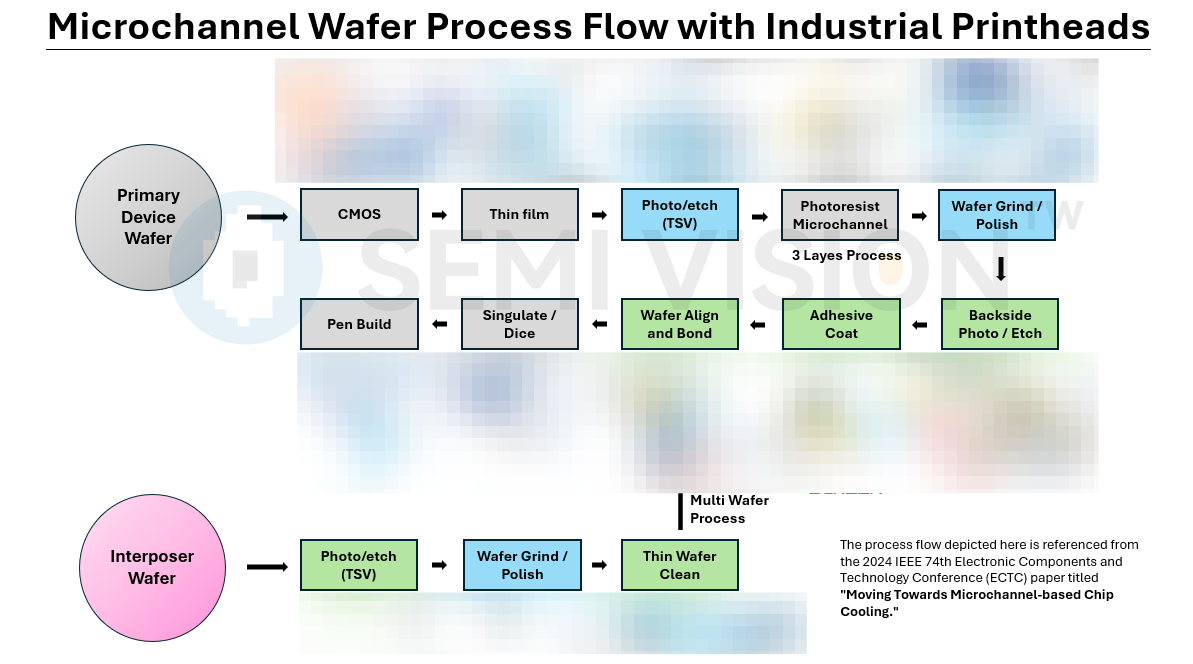
Microchannel Wafer Process Flow Explanation
Technical Significance and Application Expansion
System-Level Co-Optimization: Foundry-Led Direction for Future Thermal Packaging
Foundries now play a leading role in designingchip-level microfluidic cooling architectures, including aspects such as channel geometry, pillar layout, fluid inlet placement, and bonding interfaces. This ensures seamless integration with downstream CoWoS or SoIC system-level packaging.
TSMC’sCoWoS platformcombineshigh-thermal-conductivity RDLswith optimized TIM structures at the packaging level. It also exploresSi-lid microchanneldesigns, aiming to achieve a fully integrated packaging solution with low thermal resistance and high heat dissipation.
On thereliabilityfront, TSMC has also studied the electromigration performance ofCu/SnandCu/Ni/Sn/Cumicro-bump structures under high current density. These efforts are crucial to ensuring long-term stability of microchannel structures and thermal pillar attachments under prolonged high-temperature cycling.
Leading foundries likeTSMCare no longer passive responders in thermal design, butkey architects in AI chip thermal management. Thermal strategies are now embedded from thewafer fabrication stage, rather than being retrofitted in back-end packaging.
TSMC is actively exploring multiple thermal innovations:
Microchannel liquid cooling
Copper Pillar thermal columns
High-performance TIM materials
No-TIM architectures
Looking ahead, foundries must work closely with chip designers, packaging engineers, and system thermal architects toco-optimize chip-level heat transfer pathways, enabling AI modules to sustain extreme power densities in the era of3D ICs, chiplets, and System-on-Wafer (SoW)architectures.
The Thermal Wall Challenge of AI Chips: From Microchannel Liquid Cooling to TSMC's Chip-Level Thermal Management Technologies
As generative AI models scale beyond trillions of parameters and each training cycle consumes hundreds of kilowatt-hours of energy, the bottleneck of the AI era is no longer just compute or memory—it is heat. AI chips are confronting an invisible barrier known as theThermal Wall,which not only constrains chip performance and reliability but also pushes the limits of packaging and system-level design.

AI Era Heat Flux Challenge: Hotspots Entering Overheating Zone
According to the Intel–Purdue research presented at IEEE ECTC 2024 in“Moving Towards Microchannel‑based Chip Cooling”, modern AI chips now exhibit heat flux densities exceeding300 W/cm², with some hotspots reaching600 W/cm². Traditional cooling methods such as air and standard liquid cooling struggle to manage such intense, non-uniform heat sources effectively

Key Limitations of Traditional Cooling
Inadequate for high-density heat flux over 300 W/cm²
Poor handling of non-uniform hotspots
Leads to performance throttling and reliability issues
Proposed Solution: Silicon-Based Microchannel Cooling
Proximity to source: Embeds microchannel structures within silicon or packaging layers, minimizing thermal resistance
High convective efficiency: Microscale channels achieve elevated heat transfer coefficients
Hotspot-targeted cooling: Enables localized liquid cooling tailored to chip thermal maps
High integration potential: Compatible with 3D‑IC, chiplets, and HBM packaging formats
Practical challenges include fluid distribution uniformity, packaging stress management, and addressing CTE mismatches between materials
TSMC’s Perspective: Silicon Cooling Die and Chip-Level Thermal Solutions
“TSMC’s Direct-to-Silicon Liquid Cooling: Background and Technical Evolution.”
This solution integrates active cooling functionality directly into the chip packaging structure, with several key highlights:
Stacking a Cooling Die with the Logic Chip
A microfluidic-structured silicon die is directly stacked on top of the logic die, forming a localized liquid-cooling pathway within the package.
Co-Integration of Silicon Channels with the RDL
The cooling die is co-packaged with the Redistribution Layer (RDL). A low-temperature bonding process ensures mechanical integrity and reliable heat dissipation performance.
High-Flow, Low-Pressure Drop Channel Design
The microchannel design minimizes bends and flow obstructions, achieving significantly lower pressure drops compared to traditional cold plate systems.
Wide-Area Temperature Uniformity and Hotspot Compensation
Experiments demonstrate that the cooling die can reduce AI accelerator hotspot temperatures by over 20°C, improving overall frequency stability and power efficiency.
This approach reflectsTSMC’s system-level thinking, where thermal management is no longer seen as the responsibility of a single mechanical component. Instead, it becomes anintegral part of advanced system-in-package solutions, forming aclosed-loop thermal architecturealongside3D IC stacking, heterogeneous integration, CoWoS, and SoIC-Xtechnologies.
Heat Meets Packaging: The New Era of Integrated Thermal Design
From Intel–Purdue’s in-chip microchannel cooling to TSMC’s silicon cooling die architecture, the industry clearly recognizes: “the next front in packaging is thermal management.”
Thermal-Aware Co-Design
Thermal modeling is now woven into early design stages—alongside power integrity (PI), signal integrity (SI), and mechanical stress. Thermal-aware co-design ensures heat pathways are actively managed rather than retrofitted.
Redefining Packaging Responsibilities
Chips are no longer merely compute engines. Packaging modules must now deliver power, interconnects, cooling, and mechanical strength. As illustrated in microchannel, silicon-lid, and cooling die designs, packaging has expanded its functional scope.
System-Level Thermal Intelligence
Future packaging will likely embed thermal control algorithms—like Thermal AI Controllers—with sensors, hotspot scheduling, and fluidic control integrated directly into the chip-level cooling solution.
Shaping the AI Compute Landscape
From microchannel liquid cooling →
To embedded cooling dies →
Silicon heat exchangers →
Optimized heterogeneous thermal paths
These technologies will underpin next-decade high-performance computing—from 3D ICs to SoW strategies. The real AI thermal frontier lies not within the chip, but in whoever can first break through the Thermal Wall with advanced packaging design.
Thermal management is now a matter of packaging innovation, system-level integration, and chip-level intelligence — ushering in a comprehensive era of heat-aware design that supports extreme power-density AI modules.
What Is Thermal Budget?
In semiconductor and electronic system design, theThermal Budgetrefers to thetemperature difference between the maximum allowable junction temperature (Tmax) of the chip and the maximum ambient temperature (Tambient,max) in which the product operates.

Tj,max: The highest temperature the semiconductor die (junction) can safely operate at (e.g., 125°C or 150°C).
Tambient,max: The maximum expected temperature of the surrounding environment (e.g., 85°C for outdoor applications).
Why Is Thermal Budget Important?
The thermal budget determines whether a system can effectively dissipate heat under harsh temperature conditions. If the chip overheats, it may throttle performance, degrade over time, or even fail permanently.
Understanding Thermal Budget: A Critical Constraint in Chip and System Design
The Thermal Budget typically refers to the maximum heat dissipation capability a chip can tolerate, encompassing the maximum allowable junction temperature (Tj,max), thermal resistance, and the cooling requirements determined by the chip’s power consumption. Its significance is reflected in several key areas:
Performance and Reliability
Excessively high junction temperatures can lead to:
Clock frequency throttling
Increased error rates
Physical degradation or failure of the die
These factors ultimately shorten the lifespan and reduce the reliability of the chip.
Packaging Design Constraints
Thermal budget is consumed by various packaging-related components:
Thermal Interface Materials (TIM)
Package structure and thickness
For instance, the thermal resistance of the TIM bonding layer alone can consume 30–40% of the total thermal budget, leaving limited margin for the rest of the thermal path.
System-Level Power Considerations
High-density AI chips often exhibit Thermal Design Power (TDP) values exceeding hundreds to thousands of watts. This creates an immense demand for thermal headroom to prevent overheating and avoid hitting the thermal wall—a bottleneck that limits further performance scaling.
The thermal budget is not merely a physical metric—it's a fundamental design constraint that connects chip performance, packaging architecture, and system-level cooling. Effectively managing this budget is essential for enabling next-generation AI and high-performance computing systems.
Key Advantages of Microchannel Cooling for Thermal Budget Enhancement
Significantly Reduced Thermal Resistance
By embedding cooling channels within the chip or packaging layers, the heat conduction path is drastically shortened. Compared to traditional cold plates, this results in a substantial drop in thermal resistance.
High Heat Flux Handling Capability
Microchannel systems can sustain heat flux densities of300 W/cm² or more, while maintaining thejunction temperature within safe operational limits.
Controlled Flow & Optimized Pressure Drop
Channel geometry and manifold design allow both single-phase and two-phase cooling to achievelow-pressure drops, aligning with packaging power constraints and mechanical thickness limits.
Overall, microchannel coolingexpands the effective thermal budgetby reducing internal temperature rise and thermal jitter, ensuring greater system thermal reliability.
Challenges to Thermal Budget and Microchannel Limitations
Despite its advantages, microchannel cooling faces several limitations:
Uneven Fluid Distribution and Hotspot Management
In parallel microchannel configurations, improper manifold designs (e.g., U/I/Z-type) can lead to non-uniform flow and inadequate cooling in localized hotspots. Incorporating nanofluids may improve thermal uniformity, but adds complexity to fluid management systems.
Packaging Integration and Structural Reliability
Combining cooling channels with chip packaging must consider CTE mismatch, mechanical stress, and packaging strain. The thermal interface between TIM channels, silicon, and metal layers also consumes part of the thermal budget—sometimes more than 30%.
Complexity of Two-Phase Cooling
While two-phase cooling (boiling) provides excellent heat transfer efficiency, it introduces design complexity. Engineers must manage boiling pressure, condensation recovery, and avoid dry-out (loss of coolant contact).
Recent Breakthroughs: Advanced Solutions to Push the Thermal Budget Further
Two-Phase Embedded Cooling
A research team at the University of Tokyo (2025) developed a two-phase embedded cooling system with up to 7× the efficiency of traditional designs. It achieves a COP (Coefficient of Performance) of 100,000 and handles over 1 kW/cm² heat flux, significantly improving the chip’s thermal budget. Another preprint study reported a Critical Heat Flux (CHF) of 1,682 W/cm² on SiC chips, with a COP of 23,615, demonstrating high cooling efficiency with minimal pressure drop.
Through-Chip Microchannels
The latest research features through-silicon microchannel arrays capable of handling power densities beyond 10⁴ W/cm², while maintaining temperature rise below 60 K. This vertical design allows coolant to directly access multiple heat layers, drastically enhancing thermal budget capabilities.
Embedded Nanofluid Smart Cooling
By integrating nanofluids with optimized manifold structures, targeted cooling for hotspot regions becomes feasible. This improves localized cooling efficiency and helps extend the system’s overall thermal budget control.
Microchannel cooling—especially with embedded, two-phase, or nanofluid-enhanced systems—is redefining the boundaries of thermal design. As AI chips scale toward extreme power densities, mastering the thermal budget is no longer optional—it’s a core engineering frontier.
Beginning with the microchannel cooling technologies introduced by Intel and Purdue, it is evident that such approaches substantially enhance the thermal budget of AI chips. However, with packaging power levels continuously rising—reflected in ever-increasing TDP values and heat flux densities—there is an urgent need forhigher-efficiency and more reliable thermal solutionsgoing forward.
Technologies showing great promise for expanding the thermal budget include:
Two-phase embedded microfluidics, which offer massive improvements in heat removal efficiency;
Through-silicon microchannel designs, which drastically shorten the heat conduction path;
Intelligent nanofluid control, which helps mitigate uneven hotspot cooling;
Andco-design of packaging, involving the joint optimization of TIM, RDL, and cooling architecture to fully maximize the thermal budget.
Advancing Toward Microchannel-Based Chip Cooling: A Thermal Revolution for the AI Era
As artificial intelligence and high-performance computing (HPC) evolve rapidly, chip power density and packaging complexity have escalated to the point whereconventional cooling methods are reaching their limits. When surface-level heat flux exceeds300 W/cm², solutions like air cooling and traditional cold plates are no longer sufficient. In response, the industry is turning toward more efficient, localized thermal management strategies—among whichmicrochannel-based liquid coolinghas emerged as a leading next-generation solution.
Why Microchannel Cooling?
Conventional cooling technologies such as heat sinks, heat pipes, and cold plates are mature and widely adopted in desktops and servers. However, in high-power AI chips such as NVIDIA’s B100, Cerebras’ WSE, or AMD’s MI300,non-uniform hotspotscan lead to thermal throttling, performance degradation, or even physical failure. Microchannel cooling offers several critical advantages:
Proximity to the heat source: Microchannels can be integrated directly into the chip surface or inter-die layers in 3D stacks, minimizing thermal resistance.
High convective heat transfer coefficient: Microscale channels promote the transition from laminar to turbulent flow, significantly boosting thermal performance.
Modular design: Channel geometry and distribution can be customized to align with hotspot locations.
Adaptability to high heat flux: Both single-phase and two-phase liquid cooling methods allow microchannels to support several hundred W/cm² of heat flux.
Single-Phase vs. Two-Phase Microchannel Cooling
The research comparessingle-phase cooling(e.g., water or glycol-based coolants) withtwo-phase cooling(e.g., refrigerant boiling). Two-phase systems leverage latent heat from liquid–vapor transitions, providing much higher heat removal without requiring a proportional increase in flow rate or pressure. This makes them ideal for ultra-high-power applications, although they bring increased design complexity—including pressure regulation, condensation loops, and dry-out prevention.
Microchannel Geometry and Packaging Challenges
The geometry (rectangular, circular, serrated) and dimensions (width, depth, spacing) of microchannels impact the thermal resistance, pressure drop, and flow uniformity. Key packaging challenges include:
Managing thermal interfaces between silicon and metal cooling structures
Balancing pressure drop and ensuring fluid distribution uniformity
Designing interfaces compatible with advanced packaging (e.g., 2.5D/3D IC, HBM)
Ensuring material reliability and mitigating packaging-induced mechanical stress
The paper highlights the value of thin, high-thermal-conductivity silicon layers, paired with low-resistance TIMs and integrated joints, to improve overall cooling module feasibility within packaging constraints.
Experimental Validation and Performance Results
Thermal and fluidic performance data from various microchannel configurations showed that:
Microchannel cooling can effectivelymaintain chip hotspot temperatures below 70°C
Achievedthermal resistance under 0.1 K·cm²/W, outperforming conventional cooling by several times
Increasing channel count reduces per-channel pressure drop, though at the cost of increased flow partitioning and packaging complexity
Future Development and System-Level Integration
The study explores future applications of microchannel cooling in 3D ICs, advanced packaging, and in-chip fluidic channels. As AI chips evolve from planar to vertically stacked and heterogeneously integrated architectures, cooling technologies must evolve in tandem with chip design to address the thermal challenges of megawatt-scale computing modules.
Microchannel cooling is no longer just a topic of academic research—it is becoming a core enabler of next-generation AI packaging. By combining advances in materials science, fluid mechanics, and semiconductor packaging, this technology is rapidly transitioning into industrial adoption, offering a revolutionary leap in cooling capacity for the infrastructure powering AI computation.
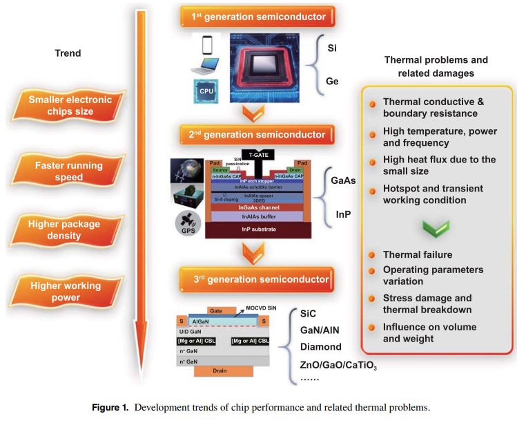
As chip size continues to shrink while operating speeds, package density, and power consumption all increase, the resulting surge in heat generation and heat flux leads to inevitable temperature rises. Once the operating temperature of chips and electronic devices exceeds their rated thresholds, a range of adverse effects — and even permanent damage — can occur. These effects include:
Thermal Failure:When a chip operates above 70–80°C, its reliability decreases by approximately 5% for every 1°C increase in temperature. The failure rate escalates exponentially as temperature rises, with overheating accounting for roughly 55% of chip failure causes.
Performance Degradation:Key operating parameters of electronic devices vary with temperature. For instance, the switching delay of insulated gate bipolar transistors (IGBTs) lengthens as the junction temperature increases, directly impacting performance.
Stress Damage and Thermal Breakdown:The differing thermal expansion coefficients of materials within a device lead to significant thermal stress under excessive temperatures. This can cause solder joints to warp, bonding wires to detach, and may even result in thermal breakdown or irreversible damage such as melting.
Impact on Size and Weight:The industry often prioritizes electrical design over thermal management, with limited attention to thermal optimization theories or enhancing cooling efficiency. Consequently, poor thermal designs can result in bulky, heavy systems, which runs counter to the industry's trend toward smaller, lighter electronic devices.

A roadmap of common cooling methods in electronics, categorized by heat dissipation capacity (horizontal axis) and cooling mechanisms (vertical axis).
The roadmap highlights four main cooling categories:
Natural Convection:
Example:Air cooling, which is the simplest form but offers limited heat dissipation.
Thermoelectric Cooling:
Example:Semiconductor refrigeration, which leverages the Peltier effect for targeted cooling.
Forced Convection:
Examples include:
Single-phase immersed cooling: Components are submerged in dielectric fluids for enhanced heat transfer.
Single-phase flow cooling: Liquid coolants flow over surfaces to carry away heat.
Phase-Change Cooling:
Techniques such as:
Heat pipes
Subcooled flow boiling
Spray cooling
Jet impingement cooling
Thermal Management Technologies and Their Corresponding Integration Levels
Effective thermal management in electronic systems requires deploying the appropriate cooling technology at the correct integration level, from the chip itself up to the data center infrastructure. The following chart summarizes the relationship between various cooling solutions—such as Thermal Interface Materials (TIMs), heat spreaders, heat pipes, cold plates, and rack-level cooling—and their corresponding points of application within the hardware hierarchy:

Microchannel Cooling: Targeted for Chip and Package Levels
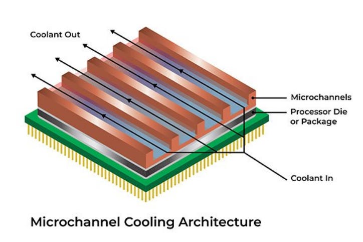
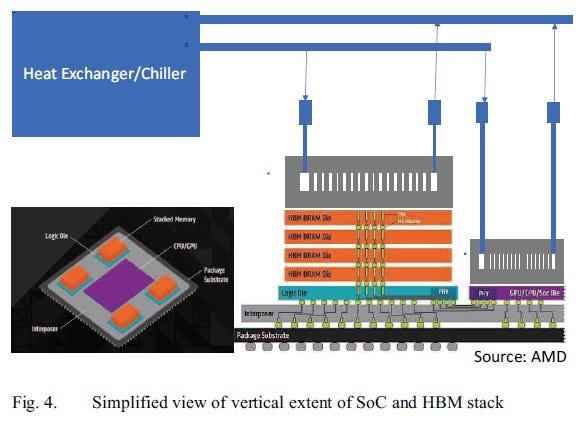
Microchannel cooling technologies are specifically designed for use closest to the heat source, such as the die level and package level. The schematic diagram provided illustrates a microchannel cold plate system, where liquid flows through microchannels placed directly above the thermal chip, separated by a thermal interface material (TIM) and managed by a manifold for fluid distribution.
The microchannel heat sink structure, often enhanced with cross-ribs, facilitates efficient heat transfer in highly confined spaces, making it ideal for high-performance computing where power densities are extreme. This approach leverages fine-structured channels to maximize surface area for heat exchange, ensuring precise and localized cooling where it is most critical.
By integrating these cooling technologies at their optimal levels, thermal management strategies can be finely tuned to meet the demands of next-generation electronics, from individual semiconductor devices to entire data center facilities.

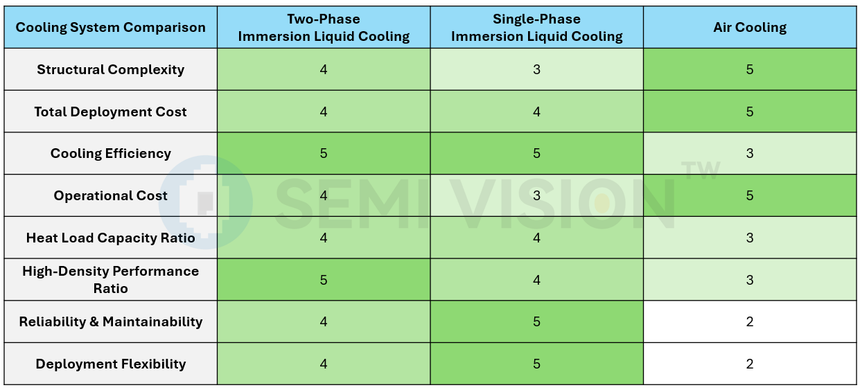
Two-Phase and Single-Phase Immersion Liquid Cooling vs. Air Cooling
Compared to air-based heat dissipation, both Two-Phase and Single-Phase immersion liquid cooling offer superior thermal efficiency. By using a non-conductive liquid medium in direct contact with heat sources, immersion cooling systems bring the cooling structure directly to the heat-generating components, enabling more effective heat dissipation.
Additionally, these liquid cooling architectures eliminate the need for:
Air-cooled heatsinks and fans on IT equipment
Traditional data center cooling infrastructure like CRAC (Computer Room Air Conditioner) and CRAH (Computer Room Air Handler) systems, as well as raised floors
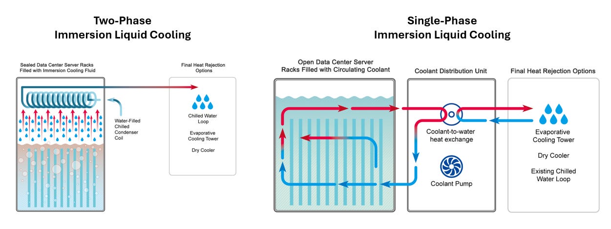
Source: GIGABYTE
Two-Phase Immersion Cooling System
In a two-phase immersion cooling system, IT equipment (such as servers) is installed within specially designed sealed tanks filled with non-conductive cooling fluid. The cooling liquid has a low boiling point. The heat generated by servers causes the liquid surrounding the heat-generating components to boil and form bubbles, creating natural convection that carries the heat away—this is the origin of the term "two-phase."
As the liquid absorbs heat and vaporizes, bubbles rise and turn into vapor. This vapor is then condensed back into liquid by the condenser coils within the sealed tank. The liquid returns to the reservoir for reuse. A dedicated environmental controller manages the continuous phase-change cycle, enabling an ongoing heat exchange process.
Single-Phase Immersion Cooling System
In a single-phase immersion cooling system, IT equipment is also submerged in a cooling tank filled with non-conductive liquid. The heat generated by the servers is directly transferred to the liquid medium through direct contact with heat-producing components.
Unlike the two-phase system, the single-phase cooling solution requires pumps to circulate the cooling liquid throughout the system. If the temperature of the liquid cannot be lowered adequately, an additional external cooling system is employed to complete the heat exchange cycle.
Because the cooling fluid used in single-phase systems has a higher boiling point and is less prone to evaporation, these systems generally do not require tightly sealed tanks or stringent environmental control measures.
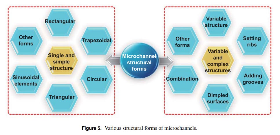
The evolution and structural diversity of Microchannel Heat Sinks (MCHSs). Initially, parallel straight channels—first introduced by David B Tuckerman in 1981—were the dominant structure in early studies. However, with the advancement of MEMS technology, researchers have expanded the design possibilities to enhance flow dynamics and heat transfer performance.
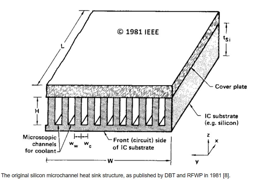
Two Main Categories of Microchannel Structures:
Single and Simple Structures:
Includes rectangular, trapezoidal, circular, triangular, sinusoidal, and other basic shapes. These are easier to manufacture but may have limited heat transfer efficiency.
Variable and Complex Structures:
Features like variable structures, setting ribs, grooves, dimpled surfaces, and combinations of designs. These configurations improve thermal performance and flow characteristics but often increase fabrication complexity.
Optimization Potential:
The structural design of MCHSs can be significantly optimized by adjusting:
Channel layout
Surface microstructures
Channel cross-sectional shapes
Geometric parameters
The continuous innovation in microchannel geometries and surface features holds substantial potential for enhancing the thermal performance of MCHSs. Further details on specific geometries and their performance trade-offs are provided
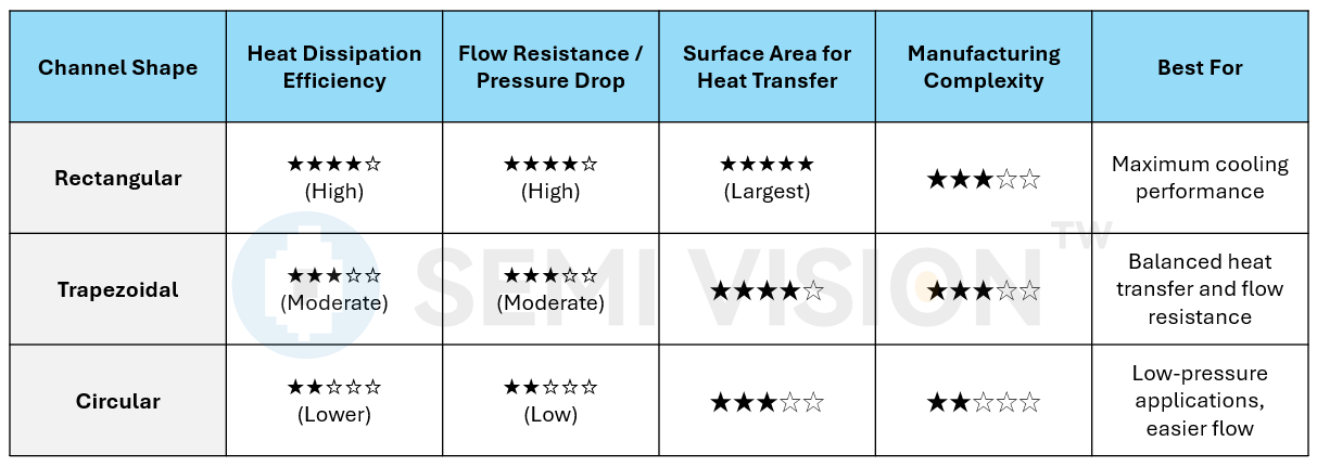
The differences among the three microchannel section shapes for MCHS

The heat dissipation performance ofMicrochannel Heat Sinks (MCHSs)varies depending on the channel section shape — specifically, rectangular, trapezoidal, and circular geometries.
Rectangular Channels (a):Rectangular microchannels typically offer high surface area contact between the coolant and channel walls, which enhances heat transfer efficiency. However, they may also present higher flow resistance, increasing the required pumping power.
Trapezoidal Channels (b):Trapezoidal channels often strike a balance between heat transfer efficiency and pressure drop. Their gradually widening cross-section can reduce flow resistance compared to rectangular shapes while still maintaining relatively good heat transfer performance.
Circular Channels (c):Circular channels usually have the lowest pressure drop among the three shapes due to smoother flow paths, but their heat transfer surface area is smaller. As a result, while easier to manufacture and more fluid-dynamically efficient, they may not dissipate heat as effectively as rectangular or trapezoidal designs.
Visualization of Microchannel Flow Dynamics

This figure illustrates the flow behavior of cooling fluids within microchannel heat sinks (MCHS), depicting the velocity distribution and pressure variation across different channel configurations.
In micro-scale environments, the laminar flow characteristics of the fluid ensure that heat transfer remains stable and highly predictable. This is a key advantage of microchannel cooling, as it allows for consistent thermal management performance critical for high-density electronics.
The diagrams show multiple inlet and outlet designs, various channel definitions, and initial flow conditions, all contributing to optimized heat dissipation by manipulating the fluid pathways within the microchannels. These visualizations are essential for understanding how design and topology influence fluid dynamics and thermal efficiency at the micro-scale.
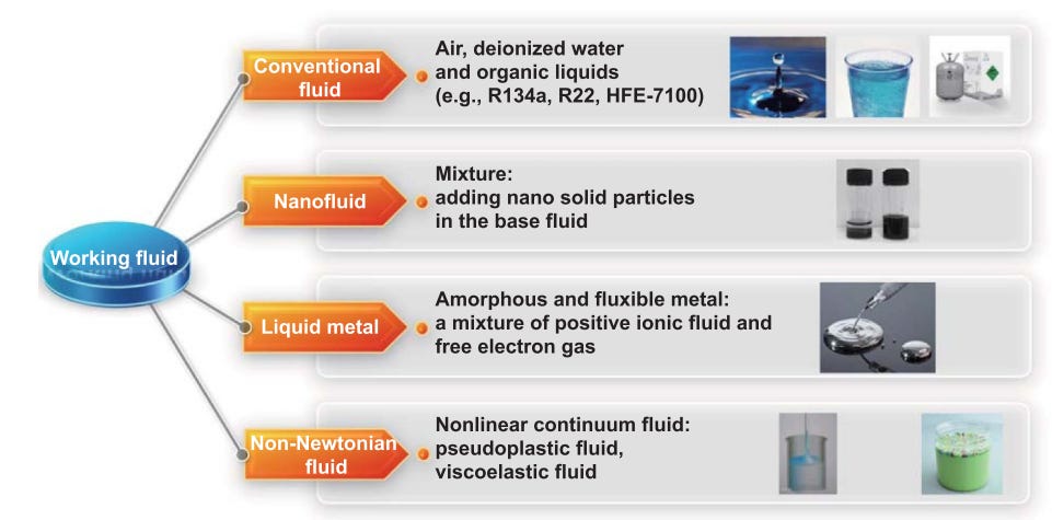
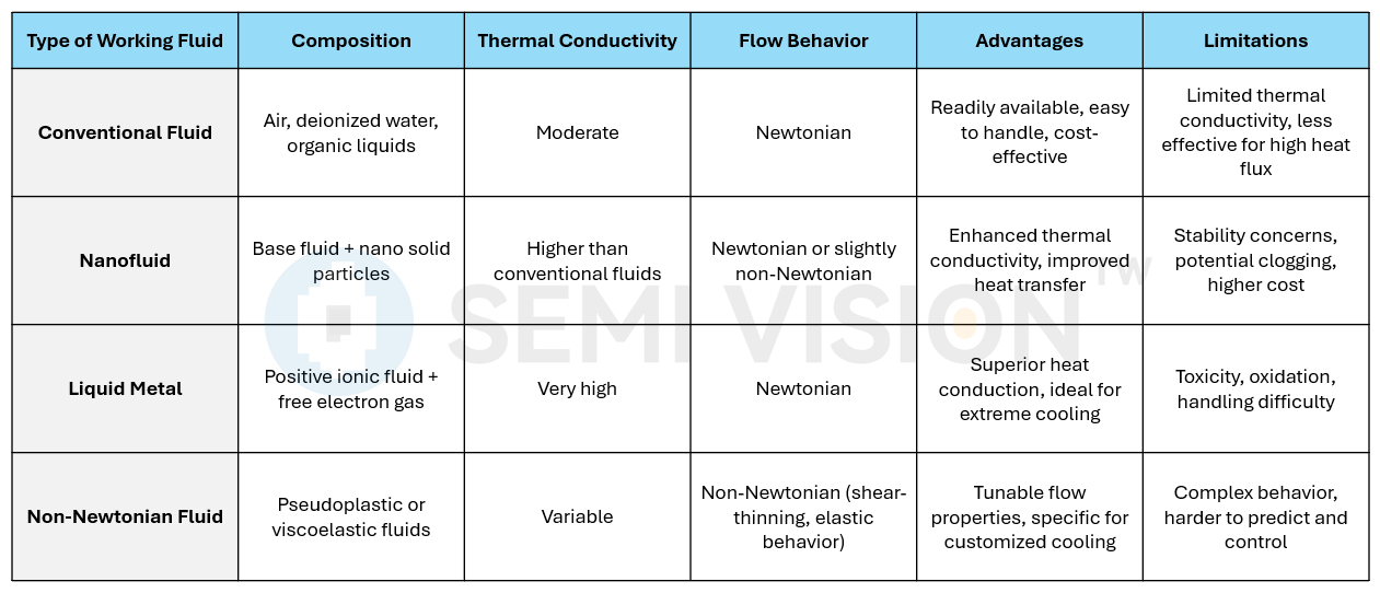
Four types of working fluids commonly applied in thermal management systems like microchannel heat sinks (MCHSs): conventional fluids, nanofluids, liquid metals, and non-Newtonian fluids. Conventional fluids such as air and deionized water are widely accessible and easy to handle but limited in thermal performance. Nanofluids, created by adding nanoparticles to a base fluid, offer enhanced thermal conductivity for improved heat transfer. Liquid metals, composed of ionic fluids and free electrons, provide exceptional thermal conductivity ideal for advanced cooling, though they present handling challenges. Non-Newtonian fluids, including pseudoplastic and viscoelastic types, exhibit unique flow behaviors that enable customized cooling strategies. Each fluid type presents distinct trade-offs, allowing tailored solutions for diverse cooling needs in electronic and microchannel applications.
Fabrication Processes for Microchannel Heat Sinks (MCHS) on Different Substrates
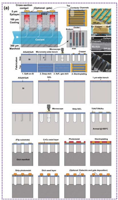
(a) Microchannel Fabrication on Silicon Substrate
This process involves creating microchannels within asilicon-based chip structure. The key steps include:
Trench Formation: Deep etching is used to formmicrometer-wide trencheson the silicon substrate, defining the microchannel paths.
Dielectric and Metal Deposition: After etching, the trenches are cleaned and coated with insulating layers such asSiO₂.
Seed Layer Deposition: ACr/Cu seed layeris applied to enable subsequent electroplating.
Electroplating and Metallization: Using photolithography and electroplating techniques,copper layersare deposited to form the channel walls and manifolds.
Optional Gate and Contact Formation: Additional steps can include forming gate structures for active devices or contacts.
Final Assembly: The microchannel layer is integrated with the manifold for fluid flow, enabling efficient cooling directly at the chip level.
This method is well-suited for semiconductor materials likeAlGaN/GaN on Si, often used in high-power electronics.

(b) Microchannel Fabrication on Diamond Substrate
This approach leveragesCVD diamondfor high-performance heat sinks, integrated withconformal porous copperto enhance capillary-driven fluid flow. The process includes:
CVD Diamond Growth: A thin film of diamond is synthesized usingchemical vapor deposition (CVD).
Laser Micromachining: Precision laser machining creates definedmicrofluidic channelswithin the diamond layer.
Porous Copper Fabrication:
Atemplate methodis used where polystyrene powders are formed and sintered to shape a porous structure.
After template dissolution, copper is electrodeposited to form theconformal porous copper.
Assembly: The porous copper is bonded to the diamond, creating a structure that supportscapillary liquid feedingandvapor escape, achieving cooling capacities up to1.3 kW/cm².
Surface Treatment: Additional steps likegold depositionimprove surface conductivity and compatibility.
This diamond-based microchannel heat sink excels in applications requiringextreme heat flux management, such as in advanced power devices and laser systems.
Together, these methods demonstrate advanced microfabrication techniques tailored for different substrate materials—silicon for mainstream semiconductor devicesanddiamond for ultra-high thermal conductivity applications.
Future Applications: Conceptual Visualization of 3D IC and On-Chip Cooling Integration
The diagrams illustrate two cooling architectures for advanced 3D-stacked chips, such asHBM (High Bandwidth Memory)andlogic SoCs:
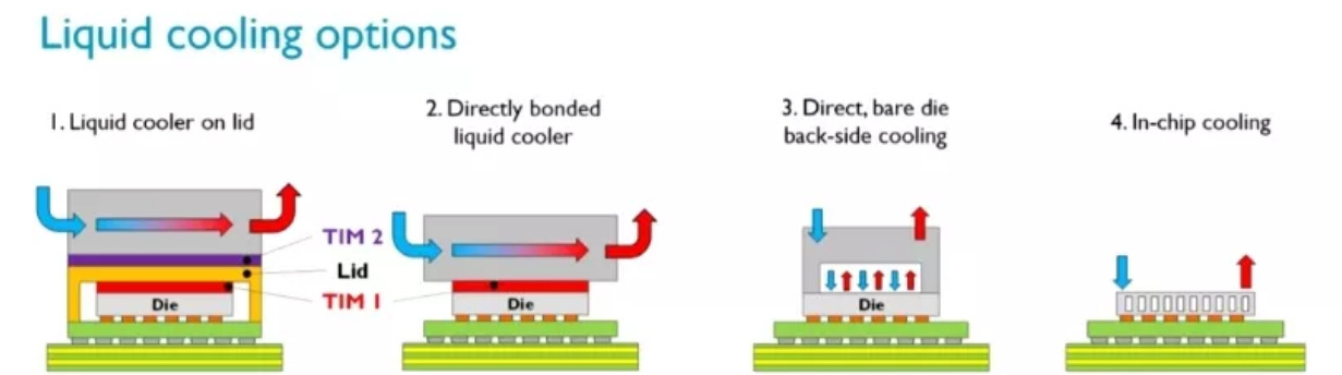
(a)represents theconventional CoWoS® package, where heat from the silicon die is transferred through multiple layers ofthermal interface materials (TIM1, TIM2)and alid, before reaching the cold plate. However, these multiple interfaces introduce additionalthermal resistance, limiting the cold plate's ability to effectively dissipate heat from localized hotspots within high-performance chips.
(b)introduces anintegrated direct-to-silicon liquid cooling approach, where liquid cooling is brought into direct contact with the backside of the silicon die. This is achieved throughmicropillar arrays etched onto the silicon, combined with asealantto create a closed cooling system within the package. This architecture significantly reduces thermal resistance and directly addresses the growing thermal challenges in high-density, high-power chip designs.
Trend Forecast: The Rise of On-Chip Microfluidics in Heterogeneous Integration
Looking forward, on-chip microfluidic cooling is expected to play a pivotal role in the heterogeneous integration and vertical stacking of 3D ICs. As AI modules evolve towards megawatt-class computing power, traditional cooling methods will no longer suffice. Microchannel liquid cooling embedded within stacked dies offers a pathway to manage extreme heat flux densities inherent in AI accelerators and advanced processors.
This approach not only enhances cooling efficiency but also enables tighter 3D integration by embedding thermal management directly into the chip structure. Such advancements are set to become a cornerstone in supporting the next generation of AI, HPC, and data center technologies, paving the way for more compact, energy-efficient, and powerful computing architectures.

Basics and Classification of TIM (Thermal Interface Material)
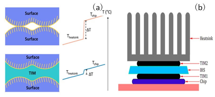
TIM (Thermal Interface Material) is used to fill microscopic gaps between the chip and the heat spreader or heat sink to improve thermal conduction efficiency. The common classifications are:

TIM 1: Positioned between thebare dieand theheat spreader (or lid).
TIM 2: Positioned between theheat spreaderand theheat sinkor chassis.
TIM 1.5: Positioned between thedieandheat sink, commonly used inlidless designs.
Thethermal resistance of TIMconsists of two components:
Bulk Resistance (R_bulk): Proportional to the material’s intrinsic thermal conductivity and thickness.
Contact Resistance (R_c1 + R_c2): Caused by incomplete contact at the interfaces.
The simplified formula for thermal resistance is:
R=BLT/(kTIM)+Rc,
whereBLTis thebond-line thicknessandk_TIMrepresents thethermal conductivityof the TIM material.
Impact of Thickness (BLT) on Thermal Performance
Thermal Resistance Increases with Thickness
With thermal conductivity held constant, the thicker the TIM layer, the higher its bulk thermal resistance, which significantly impedes heat conduction.
Moreover, if the contact resistance between surfaces is high due to poor bonding, even reducing the TIM thickness may not effectively lower the total thermal resistance.
Comparative Performance of TIM1 vs. TIM2
Under identical assembly conditions, TIM1 (die-to-lid) typically exhibits lower thermal resistance than TIM2, as it involves a smaller interface area and requires a thinner fill thickness. However, this advantage also depends on assembly pressure and the compliance of the TIM material.
By contrast, TIM2, which bridges a larger interface area and requires a thicker fill, generally presents higher thermal resistance, often becoming a thermal bottleneck in the system.
Importance of Process and Pressure Optimization
Different TIM materials—such as thermal grease, phase change materials, or metal-based TIM—exhibit varying BLT and thermal resistance characteristics under different pressures and levels of compliance.
At higher pressures, softer thermal interface materials can achieve a thinner, more intimate contact, thereby reducing contact resistance and significantly improving overall thermal performance.
Impact on Chip Thermal Performance and Thermal Budget
Accumulation of Thermal Resistance
When TIM1 and TIM2 layers each have high thermal resistance, the overall thermal resistance increases, causing the chip's junction temperature (Tj) to rise due to inefficient heat conduction.
If Tj exceeds the design's safe operating limit, it may lead to performance degradation, increased error rates, or even reliability issues.
Thermal Budget Constraints at the Packaging Level
The TIM layers represent a critical constraint in the overall thermal design.
If the TIM is not sufficiently thin or lacks adequate thermal conductivity, it will consume a significant portion of the packaging's thermal budget, thereby diminishing the effectiveness of microchannel liquid cooling or other advanced cooling solutions.
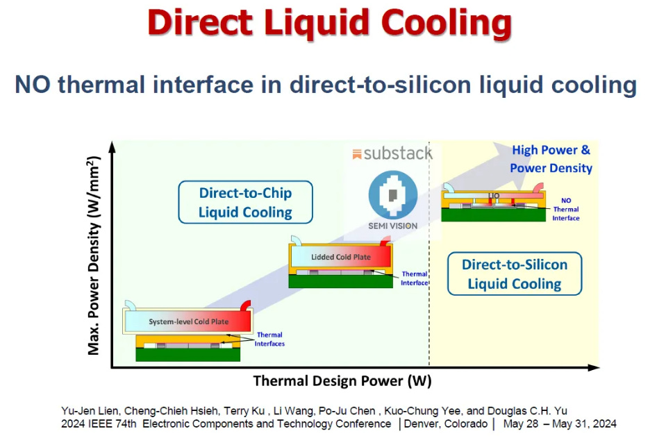
TSMC’s Rationale for Advancing No-TIM Solutions
TSMC has been actively exploring architectures that eliminate the use of TIM (Thermal Interface Materials) and has proposed various solutions such as direct water cooling and silicon cooling EMI lids. The motivations behind these developments include:
Reducing Interface Thermal Resistance and Pressure Drop
Research published by TSMC at IEEE VLSI and ECTC conferences demonstrates that etching microchannels directly on the backside of silicon or cooling lids enables efficient cooling while eliminating the thickness and contact resistance introduced by TIM layers. This approach significantly reduces the overall thermal resistance, enhancing cooling efficiency . For example, Direct Water Cooling (DWC) solutions have demonstrated heat dissipation capabilities up to2.6 kWwith a temperature differential controlled at63°C, outperforming TIM-based solutions such as SiOx TIM.
Minimizing Mechanical and Reliability Risks
Metallic TIMs or high-thermal-conductivity adhesives often suffer from thermal expansion stress, pump-out, and delamination under high-power conditions—issues especially common with polymer-based TIMs. These factors compromise long-term reliability and stability.
Direct water cooling eliminates the need for additional interface materials, reducing these mechanical risks.
Supporting Ultra-High Power Density and 3D IC Applications
As 3D-stacked chips and chip-scale power densities continue to rise, the demand for lower thermal resistance becomes increasingly critical.
No-TIM architectures are capable of supporting extreme heat flux scenarios, such as 7 W/mm² (7,000 W/cm²), which are beyond the dissipation limits of any TIM-based solution.

By adopting No-TIM designs, TSMC is addressing the thermal challenges posed by next-generation high-density, high-power semiconductor applications, particularly in advanced AI and 3D IC packaging.
Design Comparison Between TIM Thickness and No-TIM Architecture
Increasing TIM thickness leads to a linear rise in thermal resistance, while contact resistance is further constrained by bond line thickness (BLT) and surface compliance—both of which limit cooling efficiency.
Although TIM1 is thinner and performs better than TIM2, the combined resistance of both layers remains a critical thermal bottleneck.
For high-power AI chip designs, cooling architectures that eliminate TIM—such as silicon microchannel water cooling—provide significantly lower thermal resistance and a higher thermal budget.
As packaging technologies advance, TSMC’s push for No-TIM architectures stems from their multiple advantages in performance, reliability, and system-level integration, making them well-suited for next-generation, high-density semiconductor applications.


TSMC's SoW (System-on-Wafer) is a high-density, large-area heterogeneous integration platform that combines multiple chiplets, HBM, interconnects, and power modules on a single 12-inch wafer. This architecture is designed to deliver the extreme compute power and bandwidth density required in the AI era. As power consumption can easily reach several hundred watts, thermal management has become a critical factor determining the success of SoW designs.
Conditions for Microchannel Cooling Application
Microchannel cooling is primarily suitable for the following scenarios:
High Heat Flux Density (>200 W/cm²):
On System-on-Wafer (SoW) platforms, high-power AI chiplets such as GPUs or ASICs are integrated, resulting in heat flux densities reaching several hundred W/cm².
Near-Junction Cooling Requirement:
In SoW architectures, chiplets are distributed across the entire wafer. Traditional modular cooling solutions are insufficient to address the non-uniform heat distribution effectively.
Packaging Supports Microfabrication Structures:
SoW employs wafer-level assembly, providing the opportunity to directly fabricate cooling structures on the wafer itself.
These conditions align closely with the characteristics of microchannel cooling, indicating significant potential for technology adoption in SoW applications.
Key Challenges of Adopting Microchannel Cooling in SoW
While microchannel cooling holds strong potential for SoW (System-on-Wafer), several critical challenges must be addressed for successful implementation:
Uniform Fluid Distribution Across a Large Area
SoW spans the full wafer size (12 inches). Introducing microchannel cooling requires precise control of coolant flow distribution and pressure drop across this large surface area.
Conventional U-shaped or Z-shaped manifold designs are difficult to scale effectively to an entire wafer.
Structural Integration and Wafer Strength
Directly etching microchannels on the wafer surface (such as through TSVs or trenches) may compromise the wafer’s structural integrity.
Integrating liquid cooling pathways also demands highly precise bonding techniques to prevent leakage and mitigate mechanical stress on the wafer.
Process Compatibility and Reliability
SoW typically combines CoW (Chip-on-Wafer), Hybrid Bonding, SoIC-X, and RDL architectures. Integrating cooling structures must avoid interference with signal integrity and power delivery networks.
Additional risks such as liquid leakage, material CTE (coefficient of thermal expansion) mismatch, and process-packaging validation pose significant barriers to adoption.
Viable Approach: SoW + Embedded Cooling Integration Strategies
Here are several advanced implementations through which theSoW (System-on-Wafer)platform could adoptmicrochannel coolingtechnologies:
Cooling Interposer
A silicon-based interposer with embedded microchannels is placed beneath the chiplets to enable wafer-level lateral cooling.
This method can be integrated with SoIC-X + CoW (Chip-on-Wafer) architectures without requiring modifications to the chiplets themselves.
Backside Cooling with TSV Microchannels
On the backside of the SoW, through-silicon via (TSV)-style microchannels can be introduced to achieve vertical liquid cooling.
When combined with BSPDN (Backside Power Delivery Network), this enables power delivery from the top and heat dissipation from the bottom simultaneously.
Selective Zoning Cooling
To avoid processing the entire wafer, microchannels are selectively implemented in localized high-heat areas, such as GPU + HBM clusters.
This creates a hybrid liquid cooling architecture, optimizing thermal management where it is most needed.
Industry Frontline Developments and Future Possibilities
Intel:showcased its embedded microchannel technology for chiplet interposers at IEDM 2023, demonstrating integration with EMIB that could potentially enable wafer-scale packaging with efficient thermal management. This approach paves the way for high-density, large-area chiplet assemblies with built-in cooling.

2025年5月1日
TSMC:proposed a novel silicon-based cooling die with integrated liquid microchannels in its 2024 ECTC paper. This architecture aligns with the direction of System-on-Wafer (SoW) thermal design and could be a foundational component in future high-power SoW implementations.
Cerebras: while not adopting microchannel cooling, has implemented a hybrid cold plate with mechanical compression system in its Wafer-Scale Engine (WSE). This provides valuable production insights and scalability benchmarks for wafer-scale systems, serving as a practical reference point for future thermal integration.
Microchannel cooling is technically feasible for System-on-Wafer (SoW) architectures, but it requires customized thermal design, mechanical compatibility, and tight co-design between packaging and cooling infrastructure. As wafer-scale integration becomes more mainstream, thermal solutions like embedded microchannels will play a critical role in overcoming heat dissipation bottlenecks and enabling next-generation AI and HPC platforms.
Thermal Challenges and Technology Trends in High-Power AI Chip Computing
Technology Trends and R&D Directions
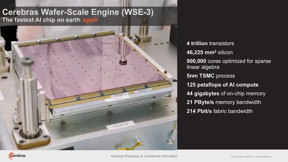
Leading semiconductor manufacturers like TSMC are actively advancing wafer-scale integration technologies. TSMC has introduced the InFO-SoW (Integrated Fan-Out System-on-Wafer) platform and is planning to realize CoW-SoW (Chip-on-Wafer-on-Substrate System-on-Wafer) stacking by 2027. This approach aims to directly stack high-speed memory (e.g., HBM4) on top of wafer-scale processors. Similarly, a report from the University of California, Riverside (UCR) highlights that Cerebras’ latest WSE-3 wafer-scale accelerator integrates trillions of transistors and hundreds of thousands of AI cores, and incorporates an internal ethylene glycol liquid-cooling loop to manage thermal design power (TDP) nearing 10 kW. Tesla’s Dojo D1 wafer-scale chip also adopts an active liquid cooling mechanism to uniformly distribute coolant across the chip surface. These examples underscore the immense thermal management challenges associated with wafer-scale AI accelerators, despite their exceptional performance and energy efficiency.
Beyond wafer-scale integration, 3D IC stacking and chiplet-based designs are also key trends. In the case of vertical 3D stacking, it shortens the distance between logic and memory layers, enhancing bandwidth and system performance. Industry studies indicate that 3D-stacked AI accelerators can achieve up to 50% improvement in performance-per-watt. On the other hand, chiplet architectures enable more flexible modular design and heterogeneous multi-core integration. For instance, AMD's Zen architecture combines multiple core complex dies (CCD) with I/O dies (IOD) to improve yield and performance. Intel employs Foveros 3D packaging to vertically stack performance and efficiency cores within a single package. TSMC also offers advanced packaging platforms such as CoWoS (Chip-on-Wafer-on-Substrate) and SoIC (System on Integrated Chips), allowing the integration of multiple dies and high-bandwidth memory into one package. NVIDIA’s Hopper GPU, for example, uses the CoWoS-S platform to integrate multiple HBM stacks with processing cores.
While these innovations significantly boost compute density and performance, they also substantially increase power density, introducing new and complex thermal design challenges that demand next-generation cooling and packaging strategies.
Comparison of Thermal Management Techniques
Microchannel Cooling:
This method involves etching micron-scale channels directly into the chip or packaging, allowing coolant (such as water) to flow through and extract heat from the source. It significantly improves thermal transfer efficiency, but its effectiveness is limited by the sensible heat capacity of the liquid. For instance, water’s sensible heat is much lower compared to its latent heat of vaporization, which can absorb up to seven times more heat during boiling than through temperature rise alone. By optimizing channel geometry and flow control, two-phase cooling (liquid/gas) can be achieved to leverage this latent heat. However, this introduces challenges in managing bubble dynamics and flow resistance.
Embedded Liquid Cooling:
This approach integrates liquid cooling directly within the package or PCB, such as placing specialized cooling blocks with microchannels atop the package. For example, Intel's recent prototype features a copper microchannel cooling block above a CPU package, channeling liquid directly to hotspots. It claims to dissipate up to 1000 watts of heat. Compared to air cooling or traditional heatsinks, this embedded liquid cooling closely couples the heat source with the cooling medium, effectively reducing the overall thermal resistance.
No-TIM Design (No Thermal Interface Material):
This strategy eliminates conventional heat spreaders or TIM layers, allowing the bare die to contact the heatsink or cooling medium directly. According to Indium Corporation, each interface layer in a thermal stack adds resistance; removing the lid can theoretically reduce the total thermal resistance between the chip and cooling solution. High-performance GPUs and ASICs often adopt lidless packages combined with thin system-level TIM 1.5 materials to enhance conductivity. Another variant replaces the silicon oxide layer with liquid metal TIM, known for exceptional thermal conductivity, effectively lowering interface resistance and boosting cooling performance.
Phase-Change Cooling:
This method uses the latent heat absorbed or released during a substance's phase change to dissipate heat. Techniques include embedding phase change materials (PCMs) or designing boiling liquid circulation systems. For example, water absorbs significantly more heat during boiling compared to sensible heating. Studies show that two-phase cooling, utilizing liquid boiling, can drastically enhance thermal efficiency. However, practical deployment faces hurdles such as thermal management of PCM, reliability concerns, and gas-liquid separation challenges.
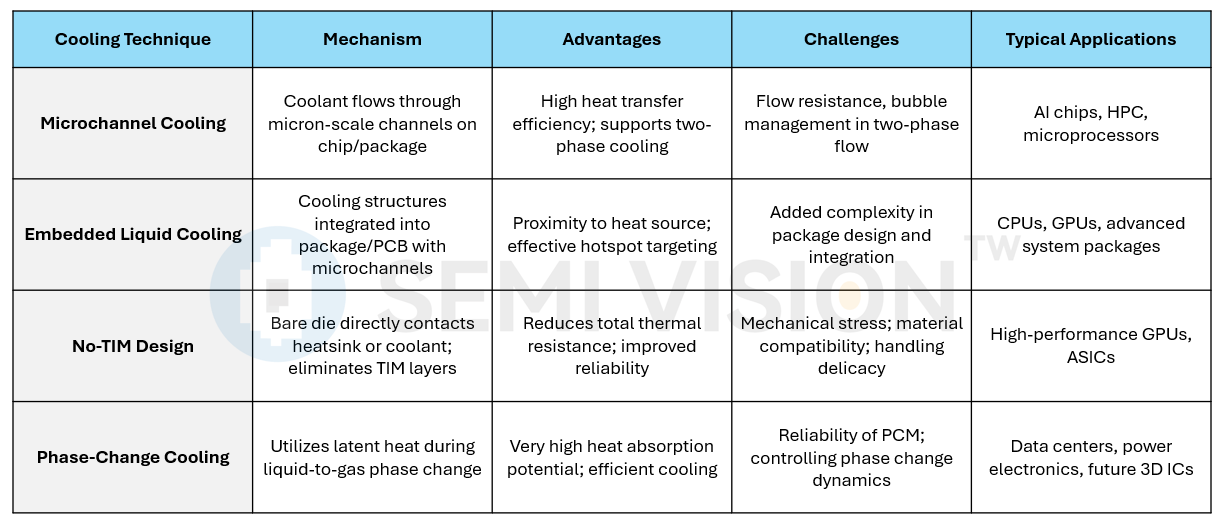
These diverse techniques offer tailored solutions for advanced cooling demands, particularly inhigh-power density AI chips and 3D ICs, where managing thermal budgets is critical.
Chip Thermal Budget and Thermal Resistance Management
Managing the thermal budget of a chip depends on the cumulative thermal resistance across multiple layers — including the intrinsic thermal resistance of transistors and metal layers, interface thermal resistance (TIM) between the die and the package (or heatsink), and the thermal resistance of external cooling structures like heatsinks and cold plates. Indium Corporation emphasizes that each additional interface layer in a complete thermal stack introduces further thermal resistance. Removing traditional package lids can theoretically lower the total resistance. In practice, even highly efficient liquid cooling systems can be bottlenecked by insufficient thermal conductivity between the chip, interface materials, and cold plate. Therefore, in high-power-density AI systems, thermal resistance across layers must be tightly controlled to prevent any single interface from becoming a limiting factor.
Conventional polymer-based TIMs (such as epoxy fillers) exhibit very low thermal conductivity, typically between 0.1–0.3 W/mK, leading to significant thermal resistance. To reduce this, high thermal conductivity fillers like diamond particles, carbon nanotubes, or metal powders are often added to create composite materials with better thermal performance. Additionally, the thickness, applied pressure, and wettability of the TIM significantly influence interface resistance. An optimal TIM must balance conductivity with long-term reliability. Because interface resistance is closely tied to process implementation, the packaging and system integration stages require rigorous thermal analysis and careful material selection to ensure effective heat transfer to the cooling system.
Industry Strategies and Technological Developments
TSMChas heavily invested in packaging-level integration. Its next-generation System-on-Wafer (CoW-SoW) platform plans to stack high-speed memory on wafer-level accelerators, leveraging InFO (Integrated Fan-Out) packaging for superior electrical and thermal performance. TSMC is also exploring silicon-based embedded liquid cooling. Recent reports indicate that directly etching water-cooling channels into the chip can handle heat flux in the kilowatt range, far surpassing the cooling capabilities of conventional packaging. Additionally, TSMC’s 3DFabric platform integrates CoWoS, InFO, and backside power delivery (BSP) technologies, improving interconnect density and reducing IR drop and power consumption, which indirectly enhances cooling efficiency.
2025年7月3日
Intelis advancing cooling and packaging in parallel. Its latest prototype features package-level liquid cooling, with copper microchannels integrated directly above the CPU package to target hotspots precisely, reportedly handling up to 1000W of thermal load. This is promising for high-end AI and HPC workloads. In its Foveros 3D stacking architecture, Intel emphasizes co-design of electrical and thermal characteristics from the outset, ensuring that the most power-hungry layers are placed at the top of the stack with specialized power connections like ODI (Omni-Directional Interconnect). This reflects a trend where multi-chip integration requires "thermal-electrical co-design" — managing heat transfer holistically from chip architecture to packaging.

NVIDIAis pursuing system-level integrated cooling solutions. Its GB200 NVL72 system employs rack-level liquid cooling, interconnecting 72 Blackwell GPUs with 36 Grace CPUs via liquid loops to create a high-density AI acceleration platform. NVIDIA also advocates for hybrid cooling (air + liquid) for data centers. On the product side, NVIDIA GPUs often use high-efficiency vapor chamber heatsinks. However, even with the impressive performance of the H100 accelerator card, cooling efficiency remains relatively low, necessitating extensive liquid cooling infrastructure to maintain safe temperatures. To address this, NVIDIA continuously strengthens hardware-software co-design, leveraging AI models and digital twins to optimize cooling and energy efficiency in large-scale systems.
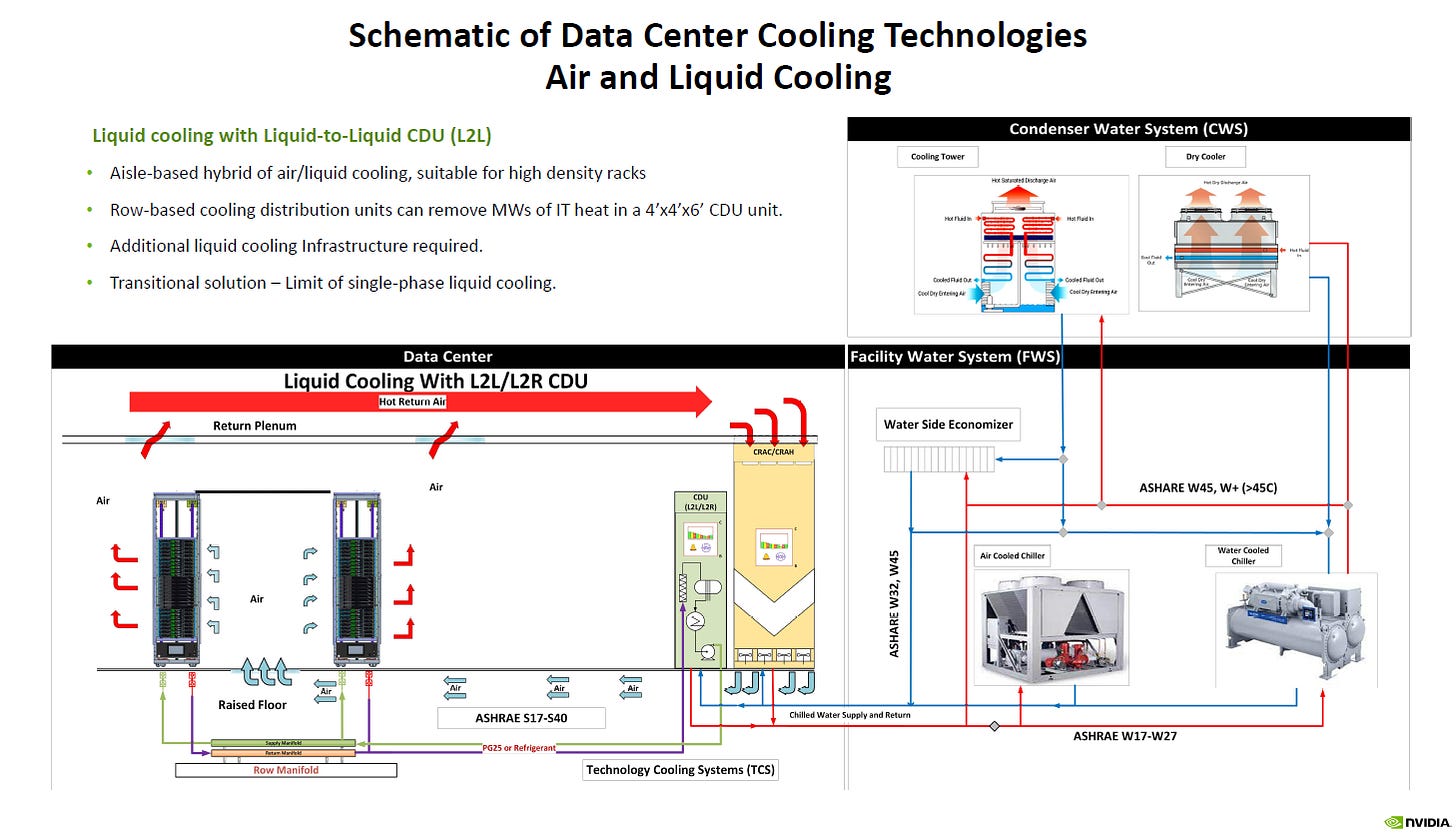

Cerebras, specializing in wafer-scale AI chips, addresses cooling internally within the package. Its WSE-3 chip integrates a dedicated glycol-based liquid cooling loop capable of handling up to 10 kW of chip power without overheating. This specialized cooling system, tightly coupled with the wafer-scale computational engine, enables Cerebras to maintain stable operations even under extreme power densities.

Future Challenges and Integrated Solutions for System-Level Thermal Management
Looking ahead, AI computing systems will impose even greater demands on thermal management, requiring holistic optimization across the chip, packaging, and system (rack) levels. Intel emphasizes that 3D stacking designs must simultaneously address all layers, coordinating the management of electrical and thermal characteristics. The core challenge lies in overcoming extreme power densities within constrained thermal budgets.
The solution involves advancing thermal-electrical-mechanical co-design, where chip architecture, interconnect packaging, and chassis-level cooling paths are optimized in unison. This includes the early incorporation of multi-physics simulations and AI-generated digital twins to predict thermal distribution and enable proactive management. Strategies like integrated packaging with backside power delivery (BSPDN) and embedded cooling channels can significantly shorten heat transfer paths.
Additionally, system-level thermal management must balance energy efficiency, cost, and reliability. This could involve hybrid cooling approaches, combining active air and liquid cooling, and the development of adaptive cooling control algorithms tailored to real-time workloads.

In summary, the thermal design of future AI systems will be increasingly complex, requiring close collaboration between chip architects, packaging engineers, and cooling system designers. Only through such interdisciplinary cooperation can the industry overcome current thermal bottlenecks and achieve more powerful and energy-efficient AI computing platforms
This summary compiles various chip cooling technologies and their heat flux dissipation capacities, measured in W/cm², along with corresponding researchers and publication years:

Key Observations:
Microchannel Cooling & Manifold Designs currently lead with heat flux capacities exceeding 1000 W/cm², highlighting their performance edge.
Backside microchannel cooling remains an industry focus due to proximity to heat sources and superior surface heat exchange.
Integrated cooling lids, liquid impingement, and 3D thermal structures are maturing toward practical deployment but require solutions for packaging reliability and cooling uniformity.
For AI accelerators and wafer-scale systems, microchannel cooling combined with liquid loops is poised to become mainstream. Future trends may introduce more heterogeneous materials and advanced structures to handle power levels in the kilowatt-class range.

SoC with Microchannel Manufacturing Process
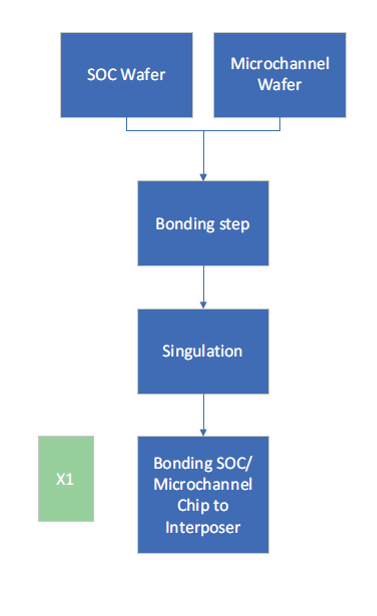
Wafer Preparation:
OneSoC wafer.
OneMicrochannel wafer.
Wafer Bonding:
Bond the microchannel wafer to the SoC wafer usingwafer-level bonding techniques, such asdirect bondingorhybrid bonding.
Singulation:
After bonding,dice the bonded wafersinto individual dies to createSoC/microchannel composite chips.
Chip-to-Interposer Bonding:
Integrate the composite chip with aninterposerduring the packaging process, preparing for furthermodule assembly.
Stacking Multiplier:
This process represents asingle-layer stacking (X1)configuration in design height.

HBM with Microchannel Manufacturing Process
Wafer Preparation:
OneHBM memory wafer.
OneMicrochannel wafer.
Wafer Bonding:
Bond the microchannel wafer to the HBM wafer, creating an HBM module embedded with cooling channels.
Singulation:
Dice the bonded wafersinto multi-layer stacked HBM dies (typically each unit contains multiple DRAM layers).
Chip-to-Interposer Bonding:
Integrate theHBM/microchannel composite dieswith aninterposer, co-packaged with the SoC in the same module.
Stacking Multiplier:
This process generally corresponds tomulti-layer stacking (X6), such as a6-layer HBM stack design.
Process Highlights and Characteristics:
By bonding microchannel wafers, die-level liquid cooling structures can be achieved, significantly enhancing heat flux dissipation capabilities.
SoC and HBM follow similar stacking logic but differ in height, tailored to their respective power consumption and cooling requirements.
Employing such processes facilitates the integration of embedded cooling technologies in CoWoS, SoIC-X, or wafer-scale packaging platforms.
Bosch Process Flow Description
- Front-End Wafer Preparation
SOC Wafer Preparation
The SoC wafer is prepared separately as theDevice Wafer, without any integrated cooling layer at this stage.
Microchannel Wafer Preparation
Produced independently as theStructure WaferorMEMS Wafer, using MEMS fabrication processes to create microchannel structures. This requires specialized manufacturing techniques but is not bonded to either SoC or HBM wafers upfront.
HBM Wafer Preparation
HBM memory wafers are also prepared separately, similar to a die-to-wafer (CoW) approach.
- Wafer Singulation
SoC, HBM, and Microchannel wafers are allsingulated individually, resulting inbare diesat the die level for subsequent integration.
- SoC and HBM Bonding to Interposer
Bond SoC Chip to Interposer
The bare SoC die is directly bonded to the interposerwithout prior microchannel integration.
Bond HBM Chip to Interposer
HBM dies are likewise bonded to the interposer separately.
- Cooling Chip Integration (Highlighted Red Zone in Diagram)
Microchannel Bonding Step (Delayed to Back-End Module Stage)
Unlike Figure 3 (referenced), in the Bosch process flow, the microchannel wafer isnot bonded during the wafer stage. Instead, bonding of the microchannel die occurs later at themodule assembly level, post SoC/HBM-interposer integration.
This delay introduces several process uncertainties:
CMP (Chemical Mechanical Polishing):
At which stage should CMP be applied? Should it be performed at the die level, interposer level, or post-assembly?
Unclear Processing Format:
Should these steps followwafer-level, panel-level, or chip-levelprocessing standards?
- Stacking Multipliers
X1 Stack:Corresponds to single-layer SoC stacking.
X6 Stack:Corresponds to HBM multilayer stacking, such as a6-stack DRAMconfiguration.
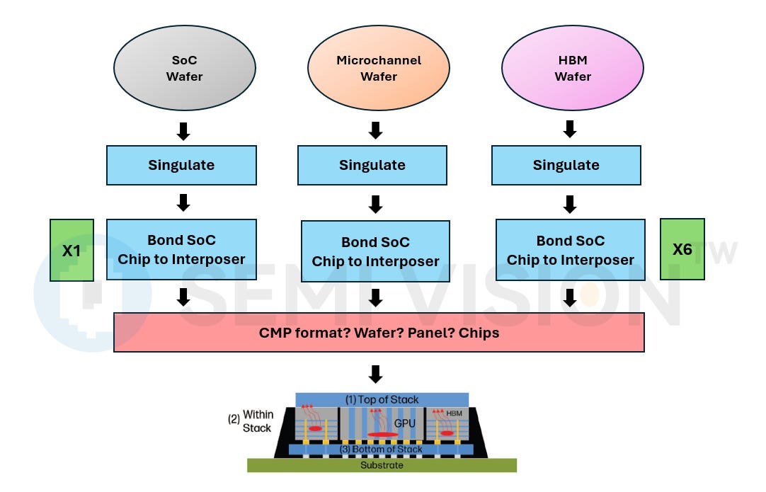
Analysis and Process Differentiation
Key Difference from Figure 3:
Bosch's approach prioritizes completing thecore chip-interposer integration first, then adding the microchannel as amodular add-onat the system level.
Potential Advantages:
Enablesmicrochannel dies to remain modular and swappable, allowing customized cooling solutions for different heat sources.
Reduces the integration burden on front-end packaging, potentially enhancingback-end manufacturing efficiency.
Critical Challenges:
CMP Planarizationand surface control need to be carefully redefined, depending on the selected integration format.
This modular strategy offersprocess flexibilitybut necessitates overcoming specific hurdles in yield, coplanarity, and thermal interface optimization.
Microchannel Wafer Process Flow Explanation

- Primary Device Wafer Process
CMOS Fabrication Stage:
Constructs the fundamental logic and driver circuit structures.
Thin Film Construction:
Deposits thermal barrier layers and conductive films, applicable for inkjet heating or other functional layers.
Through-Silicon Vias (TSV-F) Photo / Etch:
Employs photolithography and etching to create vias or pre-formed fluid channel structures.
SU8 Microchannel Formation:
Uses SU8 or other photosensitive polymers to form precise microchannel structures.
- Backside Microchannel Processing
Wafer Grind / Polish:
Thins and polishes the wafer backside to achieve precise thickness and surface flatness.
Backside Photo / Etch:
Additional photolithography and etching on the backside to form fluid inlets, vias, or heat exchange structures.
Adhesive Coat:
Applies an adhesive layer in preparation for wafer bonding.
Wafer Align and Bond:
Aligns and bonds the Primary Wafer with the interposer or other functional layers.
Singulate / Dice:
Dices the bonded wafer stack into individual devices.
Pen Build (End Module Assembly):
Final assembly stage for application modules such as inkjet printheads or other end-use systems.
- Interposer Wafer Processing
Photo / Etch:
Photolithography and etching to form fluid channels or through-holes.
Wafer Grind / Polish:
Backside thinning and surface planarization.
Thin Wafer Clean:
Cleans ultra-thin wafers to ensure high surface quality.
- Integration Logic and Features
3-Layer Process:
Utilizes multi-layer wafer stacking to integrate functions with embedded fluidic cooling structures.
Multiple Wafer Processing:
Supports mass wafer integration, enabling modular flexibility and efficient batch processing.
Technical Significance and Application Expansion
Though originally developed for inkjet printing, this process flow is highly adaptable for mass production of AI chip cooling modules, particularly for integrating backside microchannel structures in system packaging.
It represents a maturewafer-level fluidic integration platform, with conceptual value for chiplet thermal management, photonic packaging, and 3D-IC packaging solutions.


PreviousNext
TopLatestDiscussions








See all