Rapidus: The Locomotive of Japan’s Semiconductor Industry
Rapidus: The Locomotive of Japan’s Semiconductor Industry
- Source: SemiVision
- Author: SEMIVISION
- Published: 2025-07-19T22:12:45+08:00
- URL: https://tspasemiconductor.substack.com/p/rapidus-the-locomotive-of-japans Rapidus: The Locomotive of Japan’s Semiconductor Industry


Rapidus: The Locomotive of Japan’s Semiconductor Industry
Original Article by SemiVision Research ( Rapidus, TSMC, Intel, IBM, Siemens, EDA, IEEE, ECTC)

Jul 19, 2025
∙ Paid

Advanced packaging has been a widely discussed topic for years, but with the rise of chiplet architecture, the focus is shifting to how advanced packaging can be practically implemented in chiplet-based designs. This is particularly critical for many semiconductor fabs because TSMC’s leading advanced packaging technology, CoWoS, still relies heavily on reticle stitching, which in turn depends on lithography capabilities. Given the current limitations in lithography, adopting chiplet architectures combined with 3D IC integration is becoming a vital trend for the industry.
Additionally, the U.S. government has imposed restrictions on AI chip designs to prevent certain customers from circumventing export controls through intermediaries. Specifically, these regulations limit the maximum die size of AI chips, pushing Chinese semiconductor companies to pivot towards chiplet-based designs as a strategic alternative. This shift enables them to overcome die size constraints while still achieving high performance through advanced packaging and heterogeneous integration.
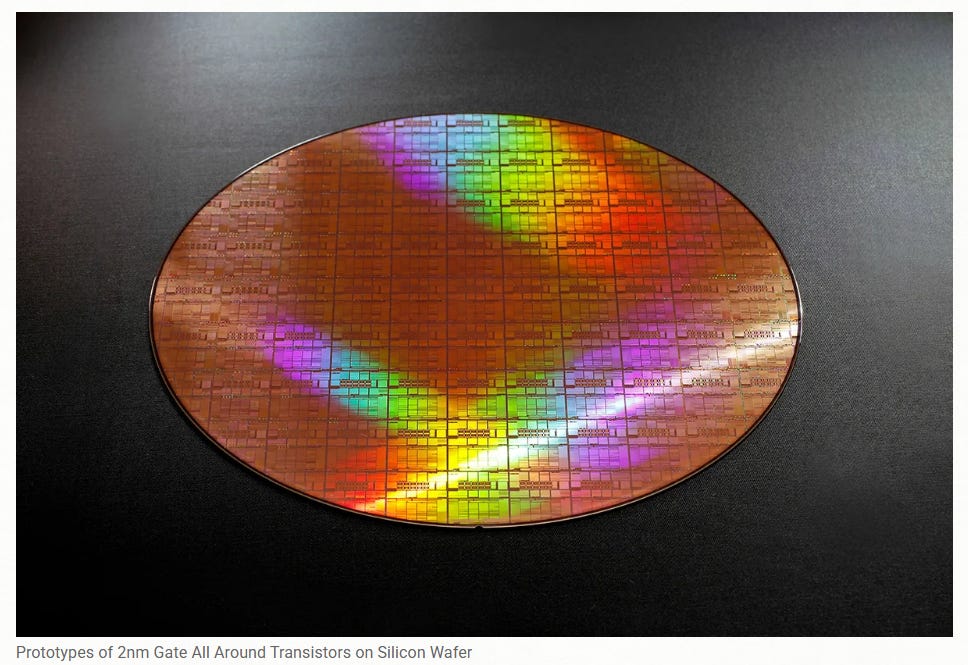
Japanese semiconductor manufacturer Rapidus has unveiled its first 2nm process chip prototype, marking its official entry into the advanced node race. The company aims to achieve mass production by 2027, though analysts note that Rapidus' current fab capacity still lags significantly behind TSMC, meaning it is not yet a serious competitor.
Meanwhile, Samsung Korea is reportedly redeploying personnel from its headquarters to Texas, USA, in an effort to accelerate the progress of its U.S. fab construction.
Backed by strong government support and investments fromSoftBankandSony, Rapidus has reached its most critical milestone since its founding. The company now sets its sights on mass production in 2027.
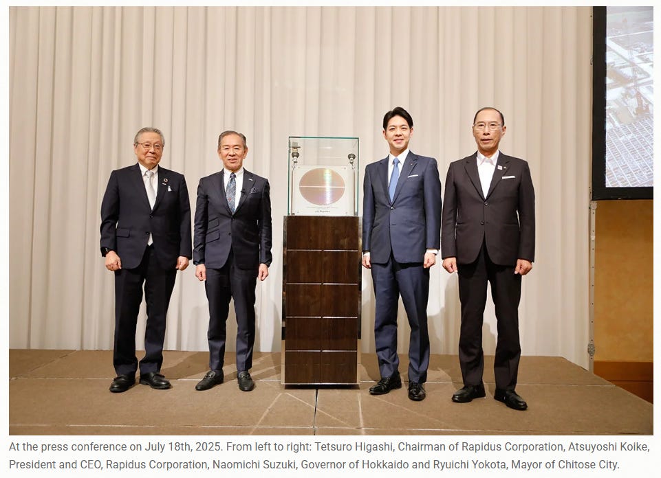
Rapidus President Atsuyoshi Koike:
“Our strong motivation to drive unprecedented global innovation was the key to our success in rapidly completing this prototype and validating the true transistor characteristics of the 2nm process.”
Rapidus, which has mobilized national government and private sector resources, is regarded as Japan’s last hope to revitalize its semiconductor industry. According to Japanese media, President Koike arrived two hours early to the announcement event, personally welcoming approximately 200 partners and potential customers.
However, the challenge remains significant. Market research firm Omdia estimates that Rapidus' current production capacity is around 7,000 12-inch wafers per month, far behind TSMC’s flagship fabs, which produce around 100,000 wafers monthly.
In addition to Rapidus, Samsung is also vying for a stake in the advanced process market. Korean media reports that Samsung has dispatched engineers to its Texas facilities, aiming to begin volume production in Q1 2026 after cleanroom activation.
Yet, foreign media point out that Samsung's 2nm yield rate remains below 30%, compared to TSMC’s approximately 60% yield. Without overcoming this yield barrier, TSMC is expected to maintain its leadership in advanced semiconductor manufacturing.
Chiplet Package Requirements —>Driven by Big Data
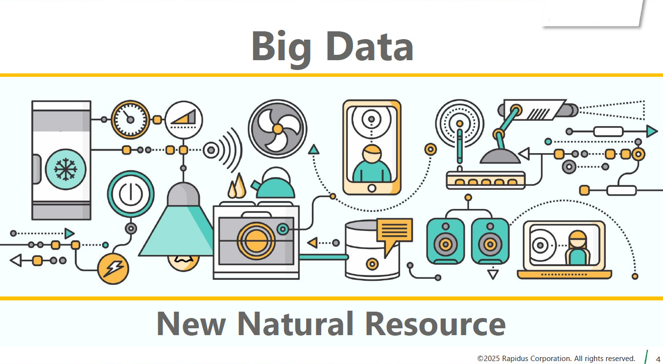
Introduction to Big Data
Big Data refers to the vast and complex volumes of data generated from various sources such as social media, IoT devices, sensors, financial transactions, healthcare systems, and more. This data is characterized by the"5 Vs":

Volume– Massive amounts of data being created continuously.
Velocity– The speed at which data is generated and needs to be processed.
Variety– Different types of data, including structured, semi-structured, and unstructured formats.
Veracity– The quality and accuracy of data.
Value– The potential insights and benefits that can be extracted.
Big Data analytics enables organizations to uncover patterns, predict trends, optimize operations, and drive decision-making based on data-driven insights.
Why Big Data Needs Advanced Chips
Processing Big Data requires immense computational power, memory bandwidth, and energy efficiency, which is why advanced semiconductor technologies are essential:
High-Performance Computing (HPC): Big Data workloads involve massive datasets that demand powerful processors, such asAI accelerators, GPUs, and custom ASICs, to perform real-time analytics and complex computations.
Parallel Processing: Advanced chips with multiple cores and specialized architectures can handle parallel data processing, which is critical for speeding up data analysis tasks.
High Bandwidth Memory (HBM): Big Data tasks involve constant data movement between memory and processors. Chips with HBM or advanced memory integration ensure faster access to large datasets, reducing latency.
Energy Efficiency: Managing Big Data at scale requires chips that are optimized for energy consumption, to reduce the operational costs of data centers.
AI and Machine Learning: Many Big Data applications leverage AI and ML, which require chips designed for neural network processing and matrix computations, such as TPUs (Tensor Processing Units).
The exponential growth of Big Data drives the need for cutting-edge semiconductor technologies that can deliver the speed, scale, and efficiency necessary for meaningful data insights in today’s digital era.
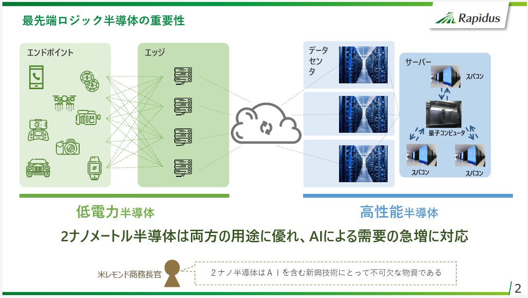
To support the high bandwidth and low latency requirements of big data processing, advanced packaging technologies have been developed. Techniques such as 2.5D and 3D integration utilize interposers and through-silicon vias (TSVs) to facilitate dense interconnects between chiplets. These configurations reduce signal path lengths, improving communication speed and energy efficiency. However, they also introduce challenges related to thermal management and design complexity.
Standardization efforts, like the Universal Chiplet Interconnect Express (UCIe), aim to establish common interfaces for chiplet communication, promoting interoperability among components from different vendors. This standardization is crucial for creating a robust chiplet ecosystem capable of addressing the diverse requirements of big data applications.
In summary, the demands of big data are driving innovations in chiplet packaging, necessitating advancements in interconnect technologies, standardization, and design methodologies to achieve the performance and efficiency required for modern data-intensive applications.
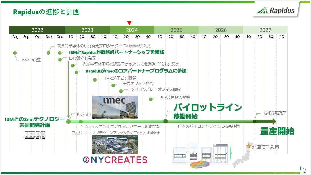
Rapidus Development Roadmap (2022–2027)
August:Rapidus is established.
December:IBM and Rapidus announce a joint development plan for 2nm technology.
Q1:Kick-off of IBM and Rapidus 2nm technology collaboration.
Q2:
Rapidus selected as a participant in Japan’s next-generation semiconductor R&D program.
Strategic partnership signed between IBM and Rapidus.
Q3:
Rapidus joins imec’s Core Partner Program.
NYCREATES collaboration begins, with Rapidus engineers dispatched to Albany NanoTech Complex.
Q4:
Rapidus announces the location of its advanced semiconductor fab: Chitose City, Hokkaido.
Groundbreaking ceremony for IIM-1 fab.
Offices established in Chiba and Silicon Valley.
Throughout the year:
Construction continues on the Hokkaido fab.
EUV equipment installation preparations begin.
Second half:
Pilot Line Operation Begins— The fab enters pilot production phase.
Technology transfer from U.S. (Albany) to Japan is in progress.
Ongoing operation of the pilot line, refining technologies and scaling readiness.
Mid-year:Technology transfer completed.
Second half:Mass Production Beginsat the Hokkaido fab.
This roadmap illustrates Japan’s national-scale effort—led by Rapidus—to re-enter the advanced semiconductor manufacturing race by achieving 2nm node mass production by 2027, in collaboration with IBM, imec, Siemens and NYCREATES.


From left to right, Dr. Mukesh Khare, general manager, IBM Semiconductors and vice president, Hybrid Cloud Research, IBM; Dr. Atsuyoshi Koike, president and CEO, Rapidus Corporation; Henri Richard, general manager and president of Rapidus Design Solutions, LLC.
For Paid Members , SemiVision will discuss topics on
Evolution of Semiconductor Packages
In an Era When PKG Determines Performance
Roadmap of Chiplet Packages
Chiplet Package Generational Classification
Marvell’s Silicon Photonics and Advanced Packaging Innovation
Design Considerations for Chiplet Packages
Japan's Semiconductor Revival and Rapidus' Strategic Partnership with Siemens
Decoding Rapidus' Vision: MFD and DMCO
The Role of PDKs: Bridging Design and Manufacturing
Why Siemens? A Strategic Choice
EDA Tools: The Infrastructure of Semiconductor Design
The Reference Flow: A Blueprint for Success
The Global Race: TSMC, Samsung, and Rapidus
Rapidus' Niche: High-Mix, Low-Volume, Ultra-Fast TAT

2025年4月4日
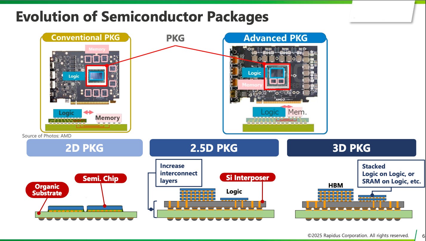
Early Stage (1990s–2000s): Multi-Chip Modules (MCMs) and System-in-Package (SiP)
Technologies:Ceramic and organic substrates with wirebond or flip-chip connections.
Key Features:Enabled basic integration of logic, memory, and analog ICs within a single package.
Limitations:Constrained by coarse interconnect pitches (>100µm), limited bandwidth, and higher parasitics, which restricted performance gains.
Primary Use Cases:Mobile devices, consumer electronics, and early network equipment.
Intermediate Stage (2010s): 2.5D Integration with Silicon Interposers
Technologies:Silicon interposers with fine-pitch Through-Silicon Vias (TSVs) enabling high-density interconnects between chiplets.
Milestones:
Xilinx:Introduced 2.5D FPGA with silicon interposers.
AMD:Deployed 2.5D integration in GPU and HPC applications with HBM memory.
Benefits:Improved memory bandwidth via HBM, reduced latency, and higher signal integrity.
Challenges:Costly interposer fabrication, thermal dissipation management.
Current Stage (2020s): RDL Interposers, Hybrid Bonding, and 3D Stacking
Technologies:Redistribution Layer (RDL) interposers, direct die-to-die Hybrid Bonding, and vertical 3D stacking.
Key Advancements:
Finer-pitch interconnects:Achieving sub-10µm pitches.
Hybrid Bonding:Reduces parasitics, boosts bandwidth density.
3D Stacking:Enables direct vertical integration for logic-logic, logic-memory, or memory-memory stacking.
Industry Examples:TSMC SoIC, Intel Foveros, Samsung X-Cube.
Advantages:Compact form factors, higher power efficiency, and massive interconnect bandwidths supporting AI, HPC, and networking.
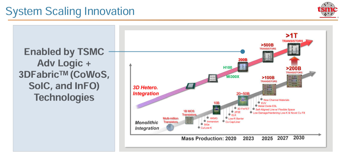
Emerging/Future Stage (Late 2020s–2030s): Direct Wafer-Level Integration and Photonic Interconnects
Technologies in Development:
Wafer-to-Wafer (W2W) Bonding:Full wafer-level stacking for even tighter integration.
Co-Packaged Optics (CPO):Embedding optical I/O within packages to overcome electrical interconnect limitations.
Chiplet Standardization:Efforts like UCIe (Universal Chiplet Interconnect Express) to enable interoperability across vendors.

2025年7月11日
Expected Impact:
Terabit-class interconnectsbetween chiplets.
Enhanced energy efficiency critical for AI clusters and data centers.
Modular system architectures enabling rapid reconfiguration and specialization.

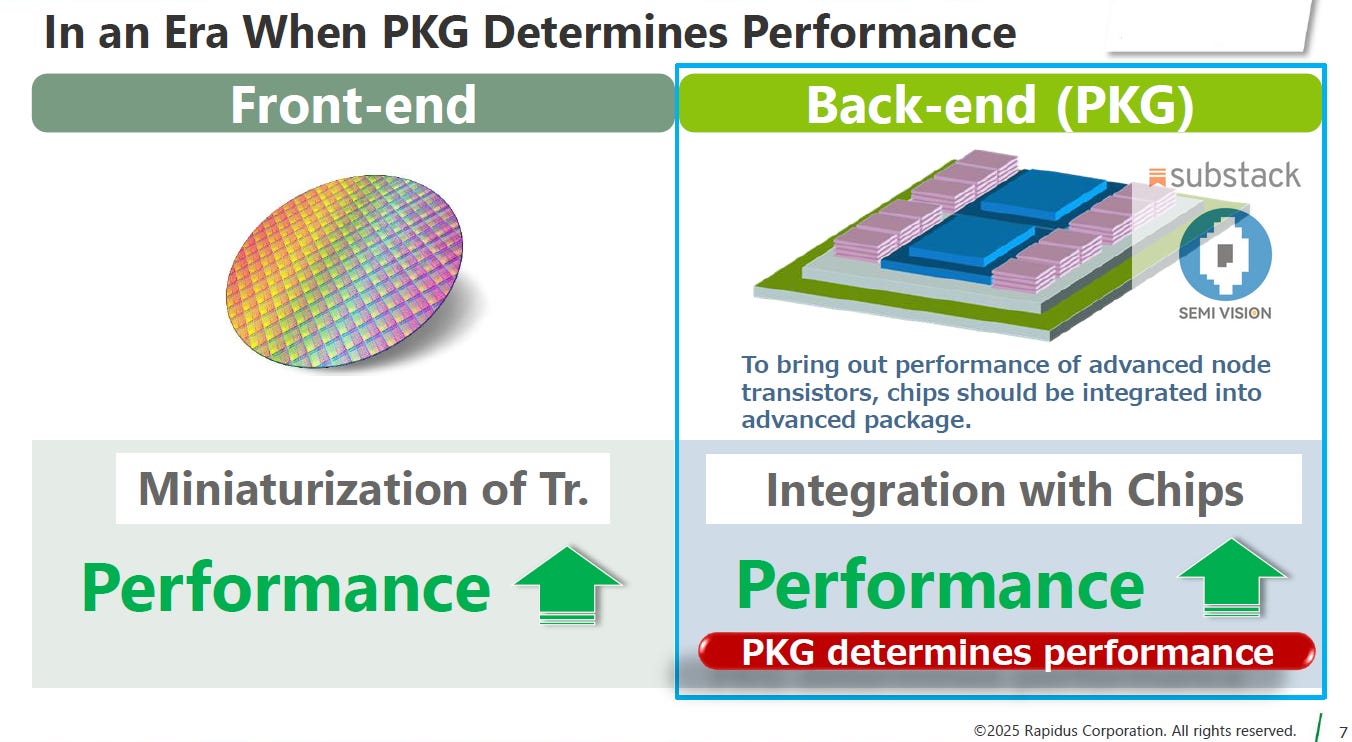
In an Era When PKG Determines Performance
A key shift in the semiconductor industry:advanced packaging (Back-end PKG)has become a critical driver of chip performance, on par with — or even surpassing — traditional transistor scaling (Front-end).
In the Front-end, performance improvements historically relied on transistor miniaturization, following Moore’s Law. Smaller transistors enhanced chip speed, reduced power consumption, and increased density.
However, in the Back-end (PKG), as we reach physical scaling limits, advanced packaging technologies now play a decisive role. Through chiplet integration, 2.5D/3D packaging, and hybrid bonding, performance gains are achieved by:
Reducing interconnect distance
Improving bandwidth density
Enhancing power efficiency
Supporting heterogeneous integration of logic, memory, and I/O
The message is clear:“PKG determines performance”— a reality especially evident in AI, HPC, and data center applications where system-level integration via packaging defines the overall computational capability.
Thus, advanced packaging is not just backend support — it is now afrontline innovation enablerfor the semiconductor industry's next growth phase.
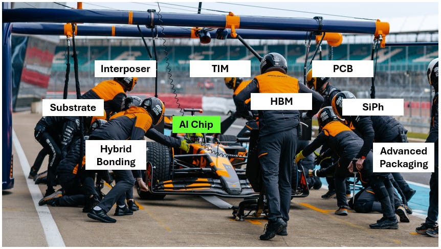
"Moore’s Law drives the 'engine,' but advanced packaging defines the 'overall vehicle performance.'
Today’s technology trend makes it clear: a powerful single core is no longer sufficient — system-level integration through packaging is the true key to leadership."
This concept through the analogy of a Formula 1 pit stop. Here, the AI chip is represented as the car — the core of computing power — while the surrounding pit crew symbolizes the critical components of the packaging ecosystem: Hybrid Bonding, Interposer, HBM, SiPh, Substrate, PCB, TIM, and Advanced Packaging.
Just as a race car's performance depends on a synchronized, efficient pit crew, an AI chip’s real-world capability relies on these packaging technologies working seamlessly together. The visual reinforces the notion that advanced packaging is the essential support system that unleashes the full speed, efficiency, and reliability of modern computing — making it the true performance determinant in the AI and HPC era.
Roadmap of Chiplet Packages


The trend in advanced packaging is increasingly dominated by chiplet integration combined with hybrid bonding, driven by the industry's demand for higher bandwidth, lower latency, and improved power efficiency.
Chiplet Integration Growth:Since 2019, chiplet-based architectures have experienced exponential growth as a preferred approach for system scaling. This is fueled by the need for flexible heterogeneous integration, where multiple dies of different process nodes and functionalities can be packaged together to optimize performance and cost.
Hybrid Bonding Acceleration:Hybrid bonding has rapidly become the key enabler for next-generation chiplet designs. Its ability to provide sub-10µm interconnect pitches and enhanced signal integrity makes it essential for dense 2.xD and 3D stacking. The data shows hybrid bonding overtaking both Si interposer and RDL technologies in publication and industry focus post-2020.

As AI, HPC, and data center applications continue to demand massive bandwidth and energy efficiency, the convergence of chiplet architectures with hybrid bonding will be the dominant paradigm. This will lead to:
More widespread adoption of 3D ICs and advanced 2.xD packaging
Increased investments in hybrid bonding manufacturing capabilities
Greater collaboration between foundries, OSATs, and system integrators to build standardized chiplet ecosystems
In summary, the synergy between chiplets and hybrid bonding is defining the roadmap for advanced packaging, setting the stage for future computing scalability.

2025年7月13日

Chiplet Package Generational Classification:
Gen 1: 2.5D Integration– Based on Si Interposer; suitable for high-bandwidth but planar integration.
Gen 2: 2.xD Integration– Leverages RDL Interposer or organic bridges for cost-effective and flexible layouts.
Gen 3: True 3D Integration– Uses hybrid bonding and Through-Silicon Vias (TSVs) to vertically stack active dies, enabling ultra-dense and high-performance architectures.
Each generational leap corresponds to both a reduction in interconnect latency and a boost in achievable bandwidth density. These developments are aligned with the roadmap from leading foundries and OSATs, pushing toward full 3D heterogeneous integration ecosystems.
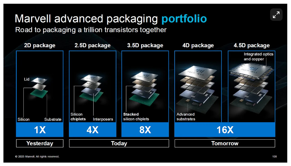
Marvell’s Silicon Photonics and Advanced Packaging Innovation
Marvell has invested heavily in silicon photonics platform development, accumulating over 8 years of mass production experience and more than ten billion operational hours in real-world deployments. This ongoing evolution enables tighter integration between photonic components and traditional electronic chips. One major outcome is the development of an optical system-on-chip (optical SoC) architecture, enabling chip-scale long-reach optical interconnects.
In advanced packaging, Marvell outlines a technology roadmap progressing from 2.5D packaging—where dies are placed on a passive silicon interposer—to 3.5D, involving more complex chip-substrate system integration, and even to 4.5D platforms, which co-integrate high-density optical and copper connections across multiple chips. According to Marvell, these 4D/4.5D configurations, combining fiber-optic and electrical engines, can support up to 16 times more compute cores, representing a packaging density several dozen times higher than conventional single-die solutions.
At the system integration level, Marvell has introduced a novel multi-chip packaging platform that replaces traditional large silicon interposers with custom modular Re-Distribution Layer (RDL) dielectric structures. This new platform features a 1390 mm² silicon base, integrates four stacks of HBM3/3E, and implements six RDL layers, enabling AI accelerators that are up to 2.8× larger than the maximum size of a single monolithic chip. These RDL packages are “tailored” to cover only the footprint required by each die, with high-bandwidth interconnects between them. This approach reduces material costs, improves yield by allowing defective dies to be replaced individually, and facilitates a more modular design.
Marvell is also working closely with packaging ecosystem partners to integrate passive components within the platform, reducing power noise. For die stacking in 2.5D, 3D, and 3.5D architectures, the platform supports bi-directional I/O, expanding the feasibility of vertically integrated, high-density chip assemblies.
In summary, from chip-scale optical interconnects to scalable multi-die packaging, Marvell’s innovations are aimed at enhancing system-level performance, density, and manufacturability, while ensuring seamless supply chain collaboration for accelerated production ramp-up and customer deployment.

2025年7月9日
Design Considerations for Chiplet Packages
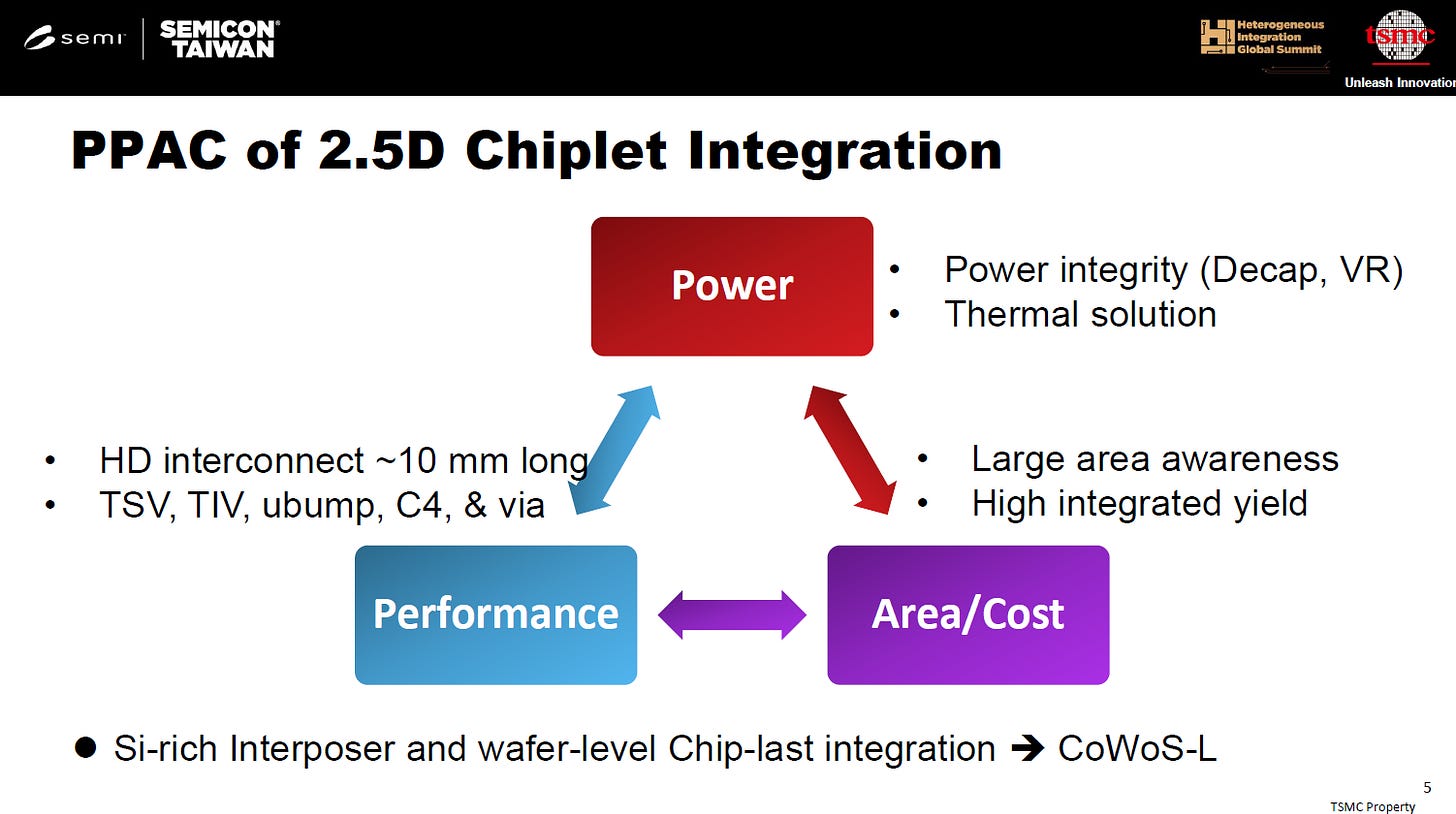
The PPAC considerations (Power, Performance, Area, and Cost) for 2.5D chiplet integration, which is essential for heterogeneous integration in advanced semiconductor packaging.
1.Power
Focuses on power integrity, ensuring stable power delivery using decoupling capacitors (Decap) and voltage regulators (VR).
A reliable thermal solution is critical to manage heat dissipation, especially in high-density chiplet systems.
- Performance
Achieved through high-density interconnects approximately 10 mm in length, supporting high-bandwidth data communication between chiplets.
Technologies involved include TSV (Through-Silicon Via), TIV, ubump, C4, and various vias to ensure efficient signal transmission.
- Area/Cost
Requires large area awareness to efficiently place multiple chiplets on an interposer.
Aims for high integrated yield to minimize defects and production costs.
The goal is to balance area efficiency and overall manufacturing cost while ensuring robust performance.
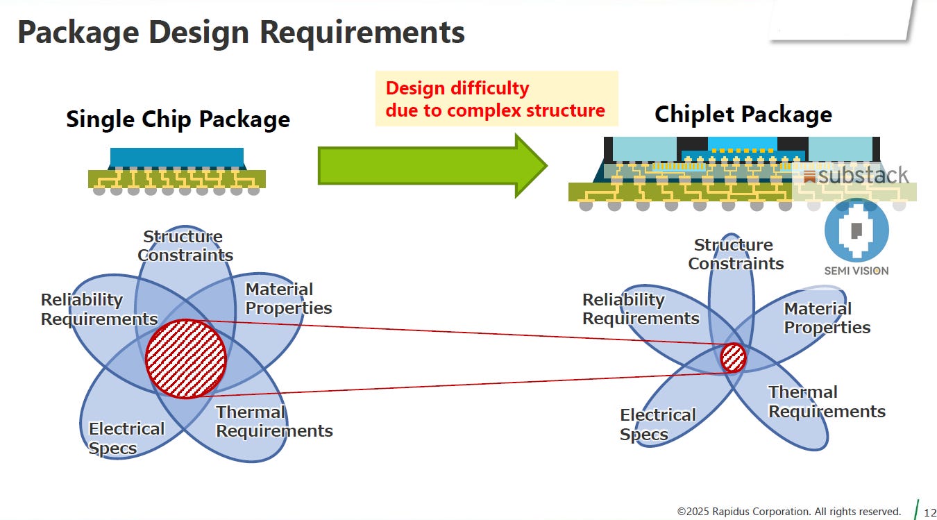
Designing advanced chiplet-based packages presents a significantly more complex challenge than traditional monolithic or single-die systems. The multi-die environment introduces new design variables across thermal, mechanical, electrical, and material domains. A robust package design must simultaneously satisfy the following critical requirements:
a)Electrical Considerations:

Signal Integrity (SI):Ensuring high-quality signal transmission by minimizing reflections, crosstalk, and impedance mismatches.
Power Delivery Network (PDN):Managing voltage drops (IR Drop), impedance control, and decoupling strategies to sustain reliable power.
High-Speed Interfaces:Maintaining performance for interfaces such as SerDes, PCIe, or proprietary die-to-die links (e.g., UCIe, XSR).

2025年7月6日
b)Structural and Assembly Constraints:
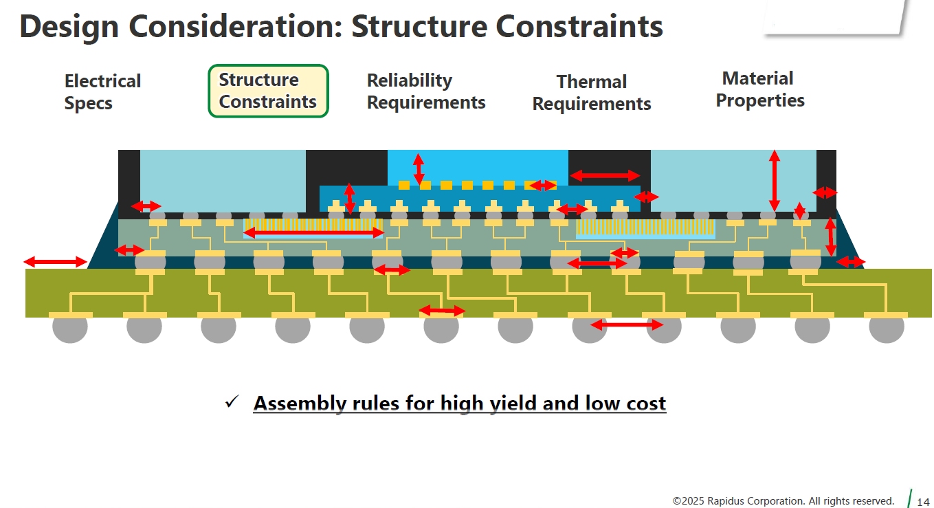
Defining co-design rules between chiplets, substrate, and interposer to maximize assembly yield.
Optimizing die placement to minimize package warpage and stress.
c)Reliability and Mechanical Stress:

Managing CTE mismatch between dissimilar materials (e.g., Si, organic substrates) to prevent warpage or cracking.
Ensuring mechanical integrity over thermal cycling and long-term usage.

2025年6月30日
d)Thermal Design:
Preventing localized hot spots through efficient heat spreading and TIM (Thermal Interface Material) selection.
Implementing package-level heat dissipation strategies (e.g., lid design, vapor chambers, integrated cooling solutions).

2025年7月9日

e)Material Selection:
Choosing materials with suitable dielectric constants, thermal conductivity, and mechanical compliance.
Coordinating material stack across chiplets, interposers, mold compounds, and underfills to meet warpage and reliability targets.

Given the multidimensional design space,Assembly Design Kits (ADKs)have emerged as a key tool. ADKs provide standardized design rules, electrical models, and process constraints tailored to the packaging house’s technology. By adopting ADKs, chip designers can reduce development cycles, improve first-pass success rates, and accelerate time-to-market for complex chiplet systems.
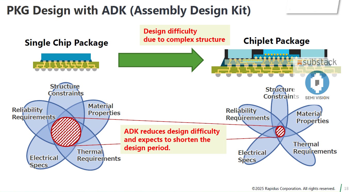

Assembly Design Kits (ADKs)are standardized toolkits provided by advanced semiconductor foundries or OSATs (Outsourced Semiconductor Assembly and Test providers) to help customers design their advanced packaging solutions effectively and accurately.
An ADK typically contains:
Design Rules & Guidelines:Specifications on die placement, spacing, bump pitch, interposer routing, and package dimensions.
Material Properties:Thermal, mechanical, and electrical characteristics of the materials used in packaging (e.g., underfill, mold compound).
Process Capabilities:Information on the assembly and manufacturing constraints, including achievable interconnect density and layer counts.
Electrical Models:Parasitic models for signal integrity (SI), power integrity (PI), and thermal analysis.
Template Files & Scripts:For design tools (EDA software) to simulate and validate the assembly design.
Co-Design References:Documentation and parameters to alignpackage, PCB, and system-level co-design.
Why ADKs are Important
Accelerates Design Time:Provides a clear and validated foundation for designers to build on, reducing trial and error.
Ensures Manufacturability:Aligns the customer’s design with the manufacturing and assembly capabilities of the foundry or OSAT.
Optimizes Performance:Helps achieve better electrical, thermal, and mechanical performance by adhering to proven design methodologies.
Facilitates Collaboration:Creates a standard communication platform between IC designers, package designers, and manufacturing teams.

Advanced packaging is no longer merely a backend process; it is now a central pillar in semiconductor innovation. As chiplet adoption expands across AI, HPC, and data center markets, the integration of packaging technology, design methodology, and ecosystem collaboration will be critical. The ongoing development of chiplet standards, such as UCIe, along with robust ADK frameworks, promises to unlock a new era of scalable and high-performance computing.
Japan's Semiconductor Revival and Rapidus' Strategic Partnership with Siemens
News: Rapidus announces collaboration with Siemens for 2nm semiconductor design
Decoding Rapidus' Vision: MFD and DMCO

According to the announcement, Rapidus will leverage Siemens Digital Industries Software's industry-standard verification solution, theCalibre platform, to co-develop Process Design Kits (PDKs) for the 2nm generation and beyond.
The Role of PDKs: Bridging Design and Manufacturing

A PDK is essentially a "design rulebook and component catalog" for creating semiconductors tailored to a specific manufacturing process. Designers use PDKs within EDA tools to efficiently create chips that can be manufactured at a given facility. In essence, PDKs serve as a critical bridge between the worlds of design and manufacturing. Rapidus aims to transform this bridge from a one-way path into a bidirectional highway. In the traditional model, foundries provide PDKs, and designers follow them. However, issues like low yield rates discovered during manufacturing often require costly and time-consuming redesigns.Rapidus' MFD/DMCO vision seeks to overcome this disconnect. By embedding manufacturability into the design process from the outset and using simulations to preemptively address issues, Rapidus aims to achieve high yield rates from the early stages of production and drastically reduce development time (Turn Around Time, or TAT), according to CEO Atsuyoshi Koike.
Why Siemens? A Strategic Choice
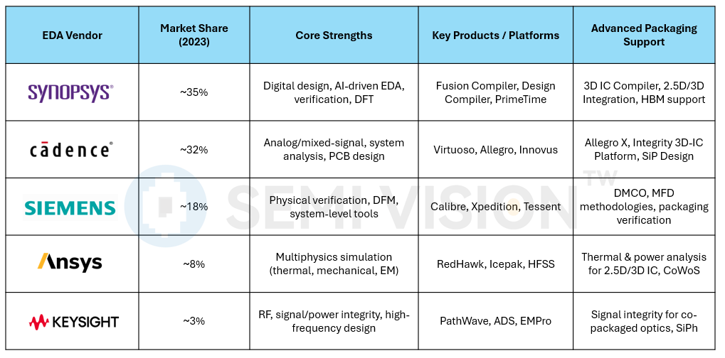
Collaboration with Siemens was essential to realize this ambitious vision. Siemens' Calibre platform is the de facto standard in physical verification, ensuring that designed circuits comply with physical manufacturing rules. By adopting a platform familiar to designers worldwide, Rapidus lowers the entry barrier for customers and encourages participation in its ecosystem. For a latecomer like Rapidus to compete with industry giants, technical prowess alone is insufficient; a sophisticated "ecosystem strategy" is critical. This partnership vividly demonstrates the strategic acumen behind Rapidus' approach.
The Siemens partnership's true value lies in addressing this yield challenge. Rapidus' vocal emphasis on MFD/DMCO reflects its strategy to tackle yield issues head-on through tight design-manufacturing integration, or "co-optimization." This approach is a bold attempt to counter the technical dominance of giants like TSMC and Samsung with business process innovation.
EDA Tools: The Infrastructure of Semiconductor Design
In the semiconductor industry, EDA tools are more than software—they are the "infrastructure" that shapes design philosophies and guides engineers' workflows. The strength of TSMC and Samsung lies partly in their extensive intellectual property (IP) portfolios optimized for their manufacturing processes and the robust design ecosystems supporting them.Rapidus must build its ecosystem from scratch. Choosing Siemens' Calibre, a "common language" for physical verification, is a highly rational first step. Beyond PDK development, Rapidus and Siemens will also work on creating a "reference flow" that integrates design, verification, and manufacturing processes from front-end to back-end.
The Reference Flow: A Blueprint for Success
This reference flow offers customers a clear roadmap: "By using our factory and following this flow, you can produce high-quality chips in record time." This reduces development risks and eliminates the need for trial-and-error design processes. As CEO Koike stated, "By openly deploying the reference flow, we aim to promote its adoption across the industry." This reflects Rapidus' strategic intent to attract partners by fostering an open ecosystem. However, the 2nm process battlefield is unforgiving, with TSMC and Samsung locked in fierce competition at this cutting-edge node.
The Global Race: TSMC, Samsung, and Rapidus
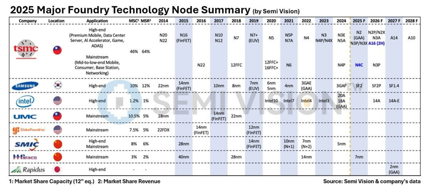
Samsung, long the industry's second player, aims to outpace TSMC by starting 2nm chip production at its Taylor, Texas facility as early as Q1 2026, aligning with U.S. government efforts to secure advanced semiconductor supply chains domestically. Yield rates are critical in this race. Reports suggest TSMC achieves around 60% yield for its 2nm process, while Samsung lags at approximately 40%. Samsung's early adoption of the Gate-All-Around (GAA) transistor structure for its 3nm process has not yet overcome yield challenges, a cautionary tale for Rapidus, which also plans to adopt GAA for its 2nm process. Overcoming these technical hurdles will be a significant challenge.

2025年5月1日

2025年5月31日
Rapidus' Niche: High-Mix, Low-Volume, Ultra-Fast TAT
While TSMC dominates with its manufacturing scale and cost competitiveness, and Samsung pursues a vertically integrated model spanning memory and logic, Rapidus targets a niche: high-mix, low-volume production with ultra-short TAT. For customers needing high-performance chips for AI or autonomous driving delivered at unprecedented speed, Rapidus' proposition could be highly appealing. This collaboration with Siemens is a declaration of Rapidus' intent to forge a "weapon" for this niche. It transcends mere factory construction, encompassing design philosophy and business models. It marks the start of a grand challenge for Japan's semiconductor industry to reclaim its place on the global stage.
2025年4月4日
Remark:Ultra-Fast TATstands forUltra-Fast Turnaround Time, referring to the ability to deliver products or services within an extremely short cycle time.
In the semiconductor and high-tech industries, TAT (Turnaround Time) typically denotes the total time required from order placement, design, and manufacturing to final delivery.
An Ultra-Fast TAT is critical for rapidly producing prototypes, implementing design changes, or accelerating production schedules to help customers shorten development cycles and capture market opportunities faster.
This capability is particularly important for:
New Product Introduction (NPI)
Advanced packaging validation
Rapid design iterations
In essence, Ultra-Fast TAT is a key metric of competitiveness in the semiconductor industry, enabling companies to respond swiftly to evolving market demands and technological innovations.



PreviousNext
TopLatestDiscussions








See all