Unlocking Precision at Scale: TSMC’s Vision for AI and HPC Test
Unlocking Precision at Scale: TSMC’s Vision for AI and HPC Test
- Source: SemiVision
- Author: SEMIVISION
- Published: 2025-07-16T21:59:11+08:00
- URL: https://tspasemiconductor.substack.com/p/unlocking-precision-at-scale-tsmcs Unlocking Precision at Scale: TSMC’s Vision for AI and HPC Test


Unlocking Precision at Scale: TSMC’s Vision for AI and HPC Test
Original Articles By SemiVision Research (IEEE ECTC , SWTest , TSMC , Teradyne , ADVANTEST , FormFactor, FiconTEC ,Surugaseiki, Nvidia, Broadcom , Marvell)

Jul 16, 2025
∙ Paid
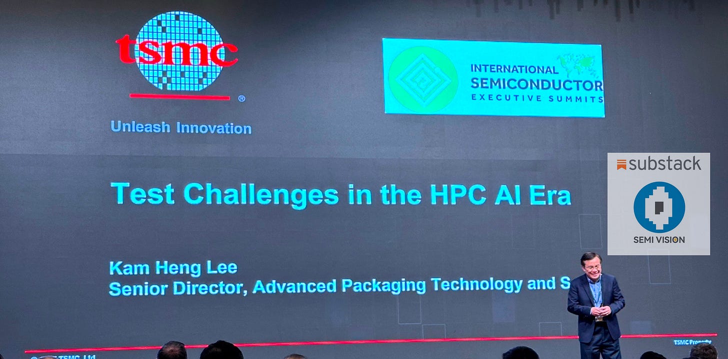
TSMC, for the first time, has addressed theTest Challenges in the HPC and AI Era, presenting valuable insights.
This presentation covers theprocess flow of CoWoS and PIC/EIC Optical Engines, which is highly important information that every reader and supply chain partner interested in learning about testing must understand.
CPO Testing Process is a critical concept, as it is essential to address how to measurePIC (Photonic Integrated Circuit),EIC (Electronic Integrated Circuit), and even theOptical Engine (OE). These topics are definitely worth discussing in depth.
The semiconductor industry is undergoing a deep transformation—one that challenges not only the physical structure of chips, but also the entire logic of how we test them.
In this post-Moore era, defined by AI chips, chiplets, HBM, and co-packaged optics (CPO), we are no longer simply chasing higher performance or transistor density. We are confronting a far more practical, pressing, and critical question:How do we test these extremely complex chips and systems?
This isn’t just an engineering problem—it’s a value chain problem. Because when testing fails, it’s not just a chip that gets scrapped—it’s the entire module, the entire packaging layer, sometimes even a multimillion-dollar AI system that crashes. And the risks begin at the wafer stage, carry through packaging and integration, and culminate in final system-level testing. Every step is a potential point of failure.
You may not have noticed, but in this world obsessed with generative AI and trillion-parameter models, the compute we rely on is actually built upon invisible foundations—the testing infrastructurethat ensures everything works as intended.
That’s why it’s time to rethink what we consider “core value” in the semiconductor industry.
For years, we’ve focused on design, process nodes, yield, and packaging—while treating testing as a supporting or even secondary activity. But that paradigm no longer holds. When a chip disaggregates into ten or more chiplets, when HBM becomes not just a memory module but a compute-enabled element, when lasers and optical engines are co-packaged with ASICs—traditional testing methods simply fall apart.
And if we continue looking at this industry with yesterday’s lens, we’ll fail to understand why test equipment is now among the fastest-growing categories of capital expenditure. We won’t comprehend why TSMC is publicly highlighting topics like probe card design, FAU alignment, anti-vibration platforms, or double-sided probing. And we certainly won’t understand how a company like ficonTEC—once known primarily for optical assembly—is now positioned at the heart of scalable CPO production.
It’s not just that testing has become harder.Testing has become the center of value.
Let’s bring it down to specifics.
Testing AI chips isn’t just about speed—it’s about thermal management, high-frequency signal integrity, contact density, and probe durability. With chips requiring thousands of pins, each carrying up to 1A of current, and thermal loads exceeding tens of watts, testing platforms are pushed to their mechanical and thermal limits. If you can’t test it accurately, you can’t ship it. And if you can’t ship it, you risk system-wide failures, customer returns, brand damage—or losing entire AI cluster orders.
You might think memory is simpler—but not anymore. As HBM stacks begin incorporating logic dies—controllers, processors, and even embedded compute—quality can no longer be judged on a memory-only basis. With the emergence ofcustom HBMarchitectures, traditional DRAM testing falls short. New strategies must test memory and logic in tandem.
Now consider silicon photonics and CPO. From a single PIC die to EIC integration, to FAU attachment, to a fully integrated CPO module—this isn’t just a packaging problem. It’s atesting problem. How do you ensure optical alignment remains precise even under vibration? How do you perform double-sided electro-optical probing? Can your test platform support both grating couplers and edge couplers on the same station? If not, your throughput won’t scale to meet the demands of the AI era.
These aren’t hypothetical engineering puzzles. These are very real, very urgent questions being asked by NVIDIA, Intel, TSMC, and Samsung as they prepare next-generation platforms for hyperscalers and global customers.
The answers lie in testing.
Over the next sections, we’ll dig into these frontline challenges:
– The extreme probe card requirements of AI chips
– KGD strategies for HBM before packaging
– Double-sided alignment for SiPh wafer testing
– Stability in optical engine assembly
– The value of RWAT, WLCP, and AST for early defect screening
And more importantly, we’ll expose the players who are winning in this new testing economy.
WhyTEL’s wafer prober is becoming the entry ticket for AI chip testing.
WhyAdvantestcontinues to expand its footprint in the HBM test market.
WhyFormFactor’s high-frequency probe cards and optical alignment platforms are being adopted across the global CPO ecosystem.
WhyMPIis carving out a strong position in photonic test.
WhyficonTEC’s evolution from assembly automation to the heart of CPO test platforms is a journey no one in the industry can ignore.

2025年4月15日
And whySuruga Seikiis becoming a foundational enabler in establishing the precision alignment ecosystem for silicon photonics testing—bridging wafer-level and module-level stages with nano-scale mechanical stages, optical benches, and active alignment systems that now serve not only research labs but also production environments for PIC-based systems.
Furthermore,Foxconn Research Instituteis quietly but steadily investing in the next wave of silicon photonics innovation—developing modular photonic engines and pioneering materials platforms such as Lithium Niobate on Insulator (TFLN), electro-optic polymers, and Silicon-Organic Hybrid (SOH) integration. These efforts are not only expanding Foxconn’s presence in data center optics and AI infrastructure, but also positioning it as a strategic player in the convergence of photonics and advanced packaging at scale.
From wafer probing to AI-centric optical modules, these players are rewriting the rules of the test and measurement domain—and reshaping the foundations of the next generation AI infrastructure.
This is not just a new chapter in testing.
This is the new logic of value.
Behind all of this lies a profound transformation—one that is redefining what constitutescore competitivenessin the semiconductor industry. And at the heart of this transformation, it’s no longer about process nodes, design IP, or even advanced packaging materials. It’s about this simple truth:Who can test chips more accurately, more efficiently, and more comprehensively.
This is the new battleground. And the content you’re reading now is your invitation into its deepest waters.
Testing is no longer a verification step—it is the value itself.
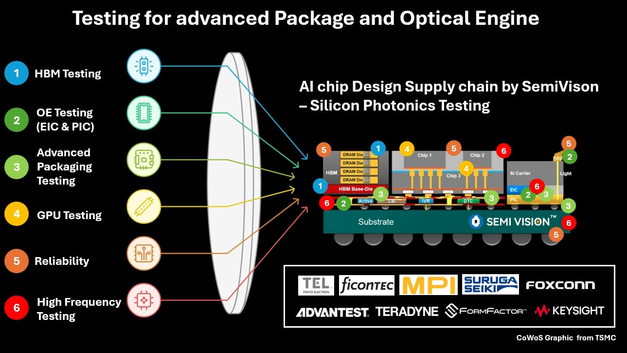
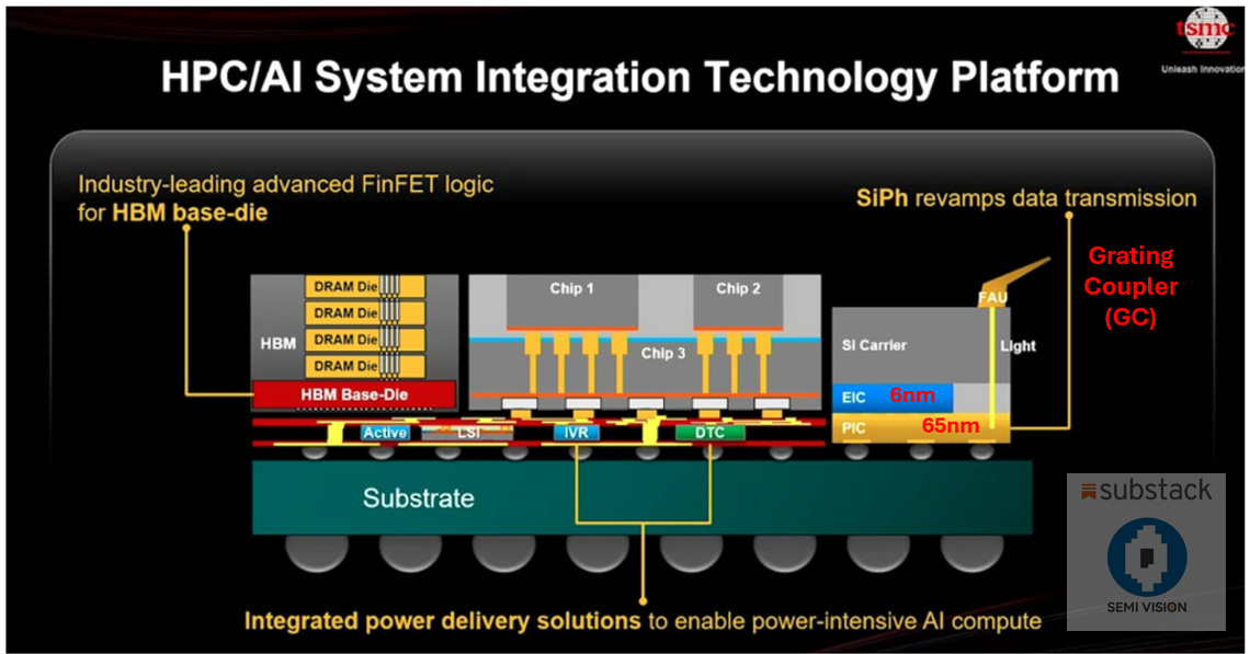
When we revisit the system integration platform diagram, we cannot just fixate on familiar keywords like HBM, GPU, or Optical Engine. While these are undoubtedly the hotspots of advanced packaging, if we aim to truly grasp the essence and complexity of system-level integration,testing and reliability validationemerge as the most overlooked, yet most decisive factors for yield and manufacturability.
In this integration platform presented by TSMC, we can identify three major technological vectors:
Vertical stacking of high-bandwidth memory (HBM) and logic;
Horizontal chiplet integration across a multi-die system;
Incorporation of a silicon photonics (SiPh) platform to enable next-generation optical interconnects.
2025年6月2日

2025年5月27日

2025年5月22日

2025年5月14日
However, each of these domains—regardless of how cutting-edge they are—requires a rigorous, layered, and well-orchestrated testing strategy to become viable products.
Take HBM for example: testing isn’t just about validating individual DRAM dies. It involves validating the full stack along with the logic base-die. That means checking TSV conductivity, thermomechanical stress integrity, and power-sequencing stability under real-world load conditions. This class of testing demands high-speed probing stations and integrated thermal test systems, where leading suppliers like Teradyne, Advantest, and FormFactor dominate. Increasingly, these companies are deployingAI-driven adaptive test platforms, capable of real-time optimization during test execution.
Now consider the central logic die. Testing here is even more demanding. With embedded IVRs (Integrated Voltage Regulators), advanced PDNs, low-loss SerDes (112G/224G), and digital control blocks all operating in harmony, traditional scan and BIST strategies fall short. Instead, test frameworks must integrate DFT-aware simulations, high-speed signal feedback systems, and monitor elements likeBuilt-In Monitoring (BIM)across multi-layer RDLs. These are not accessories—they’re foundational to the new testing architecture.
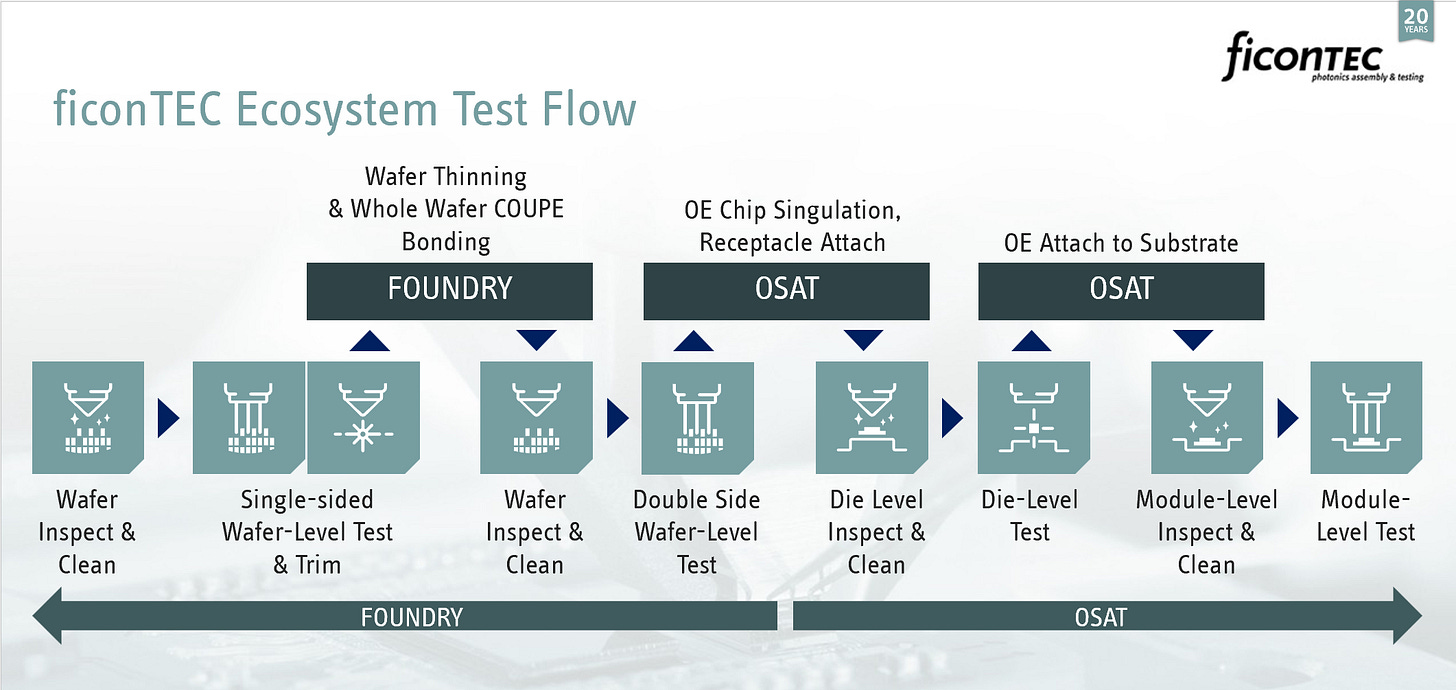
The most complex layer, however, lies inOptical Engine Testing. This involves not only validating the co-functionality of EICs (Electronic ICs) and PICs (Photonic ICs), but also measuring the physical integrity of the optical path: insertion loss, coupling efficiency, return loss, and ultra-precise fiber-to-chip alignment via Grating Couplers (GC) or Edge Couplers. Traditional electrical ATE platforms are not equipped to handle this. Instead, purpose-built systems from vendors likeficonTEC,MPI, andEXFOoffer dual-sided wafer probing, six-axis optical alignment, optical power metrology, BER analysis, and adaptive coupling scan functionality.
Importantly, these tests don’t stop at the point of measurement—they extend intoreliability qualification. This includes thermal cycling (TCT), humidity testing (HAST), high-temperature storage (HTS), and mechanical stress simulations (drop, vibration, etc.). When optical engines are co-packaged with bare logic dies, even the mismatch in coefficient of thermal expansion (CTE) becomes a system-level reliability threat. Internal stress distributions during thermal shifts can directly destabilize optical performance and lifetime.
From HBM, to chiplets, to SiPh modules—each component demands a full-stack test strategy and validation flow. Without this layer of systems engineering, even the most advanced packaging and materials cannot be translated into real-world, volume-production success. Going forward, system integration is no longer just about design and packaging—it’s aboutTest & Qualification Co-Designbecoming part of the engineering flow from day one.
In our upcoming SemiVision deep-dives, we’ll be covering:
Strategic roadmaps of leading test equipment vendors
New challenges in HBM 4 and 4E testing
Optical coupling and metrology breakthroughs in SiPh modules
The evolution of reliability qualification standards for system-in-package (SiP) platforms
Stay tuned—because in this era, those who understand testing, understand the future.
For Paid Members, SemiVision will discuss topics on
Advanced Package Testing(HBM, Chiplet, Optical Engine,Full Module)
Key Testing Strategies for Chiplet Systems: The Value and Implementation of Distributed Inline Testing
Probing Test Challenges and Technologies: A Critical Pillar in the Era of Advanced Packaging
The New Frontier of Advanced Testing: Why TSMC Is Talking About “Thermal Challenges”
Thermal Performance: Wafer-Based vs. Singulated Die Testing
Test Challenges and Systematic Strategies in the Era of Advanced Packaging: A Full-Chain Test Approach from HBM to CPO
Four Key Challenges and Technical Barriers in Mass Production Testing of Silicon Photonics (SiPh)
TSMC’s Strategic Approach to Silicon Photonics Testing
AI-Driven End-to-End Test Chain Transformation
AI/ML-Driven DFT and Test Optimization: Ushering in the Intelligent Era of Semiconductor Testing
Test Equipment Vendors and Market Opportunities
Advanced Package Testing(HBM, Chiplet, Optical Engine,Full Module)
This diagram illustrates a highly integrated HPC/AI system packaging platform, spanning from left to right: custom HBM memory modules, multi-die SoC architecture, heterogeneous power and logic control modules, and finally, a silicon photonics-based communication module (SiPh Optical I/O). The test requirements across such a system are vast and complex—each component and sub-module demands specialized testing equipment and methodologies at different stages. The following sections summarize the key testing needs and challenges based on the system segmentation shown in the diagram:
1.HBM Stack and Base-Die Testing
DRAM Die Testing
Objective:Ensure each DRAM die is free of retention errors, bit failures, and faulty cells.
Test Stages:Wafer-level CP (Wafer Chip Probing), and Known-Good-Die (KGD) validation before stacking.
Challenge:Once dies are stacked, defects are no longer isolatable. Thorough early-stage testing is crucial to avoid total module scrap.
HBM Base-Die Testing
Objective:The base die is often fabricated on advanced logic nodes (N7/N5/N3) and may include memory controllers or PIM (Processing-in-Memory) elements.
Test Requirements:Combined logic and memory interface validation in co-simulation environments.
Challenge:Cross-domain test support—both digital vectors and DRAM transaction emulation must be validated within one test environment.
2.Chiplet SoC Region (Chip1/Chip2/Chip3) and Interposer Testing
Inter-Chiplet Interconnect Testing
Objective:Ensure μBump or TSV-based interconnects are free of opens, shorts, and excessive signal loss.
Stages:Wafer-Level CP and Assembly Test (AST).
Challenge:High-density routing demands high-frequency probing and robust die-to-die scan path validation (e.g., scan chain across die boundaries).
Interposer (e.g., Chip3 or LSI) Testing
Objective:Validate any routing logic or I/O functionalities embedded in the interposer.
Challenge:Interposers often lack dedicated test access, requiring passthrough or bypass loop designs to enable structural testing.
IVR and DTC Testing
Objective:Ensure stable voltage regulation and fast thermal response—failure may cause system instability or thermal shutdowns.
Test Needs:
Power delivery and conversion validation
Thermal feedback and logic control correctness
Test point access despite shielding layers
3.EIC/PIC + Optical Engine Testing (Si Carrier Module)
EIC (Electronic Integrated Circuit) Testing
Objective:Validate driver circuitry, digital logic, and SERDES transmission.
Stages:Wafer CP, die sort, and final test (FT).
Challenge:High-bandwidth requirements necessitate support for PAM4 and other signaling formats, alongside automation-ready probe systems.
PIC (Photonic Integrated Circuit) Testing
Objective:Verify modulators, demuxes, waveguides, and photodetectors.
Key Metrics:Insertion loss, reflectivity, modulation depth, optical bandwidth, BER.
Challenge:
Sub-micron alignment precision for optical coupling
Power/temperature stabilization during optical measurements
Co-simulation and co-testing with EIC (electro-optical synchronization)
FAU and Grating Coupler Testing
Objective:Confirm accurate fiber alignment and stable coupling efficiency.
Test Process:Requires six-axis alignment systems, ultra-stable platforms, and thermal drift compensation.
Challenge:A misalignment of ±1 μm can cause >1 dB optical loss, critically degrading optical performance.
4.Full System Module Test Stages
AST (Assembly Test)
Objective:Verify module-level power delivery, functional IO paths, and optical interface integrity.
Includes:
Power-ground leakage testing
High-speed pattern generation for interconnects
Optical loopback verification
FT/BI/SLT (Final Test, Burn-In, System-Level Test)
Objective:Guarantee production quality and long-term reliability under operating stress.
Scope:
Full system logic validation
Stress and environmental testing
Emulation of real-world workloads and thermal conditions
This platform exemplifies the most advanced system integration in today’s semiconductor landscape—from memory and logic to power and photonics. Each layer introducesnew challenges in testing that go beyond electrical verification, requiring a comprehensive approach that encompasseselectrical, optical, and mechanical domains.
From wafer-level testing to final system qualification, every step must evolve alongside the complexity of integration. As these platforms scale into commercial volumes,the ability to solve these test challenges will determine who leads the value chain in heterogeneous integration.

Key Testing Strategies for Chiplet Systems: The Value and Implementation of Distributed Inline Testing
As the semiconductor industry embraces the Chiplet paradigm and heterogeneous integration, traditional single-die test processes are no longer sufficient. Each Chiplet may come from different process nodes, design teams, or even foundries, and when assembled into a complete module using advanced packaging technologies such as CoWoS or SoIC, a single defective die can jeopardize the entire system. To ensure overall yield and cost efficiency, the industry is now adopting amulti-stage, distributed inline test strategy—a crucial evolution in modern chip manufacturing.
This approach spans from post-RDL wafer testing to post-assembly module validation and is complemented by final outbound quality assurance tests, forming a comprehensive test chain.

- RWAT (Wafer Acceptance Test)
RWAT serves as the first checkpoint in the distributed inline test flow, executed after the Redistribution Layer (RDL) is completed. This stage aims to identify structural and electrical anomalies early in the process, including:
Power/ground shorts or leakage
uBump delamination
Cracks or fractures in the silicon interposer
Detecting these issues early is essential; if overlooked, they can result in catastrophic failures during later assembly or even after shipping. Because RWAT occurs relatively early, test costs are comparatively low, making it a highly effective filter to prevent defective wafers from entering high-cost packaging steps. In essence, RWAT plays a vital role in reducing risk and preserving downstream value.
- WLCP (Wafer-Level Chip Probing)
Following RDL and wafer reconstitution, WLCP is conducted during wafer-level packaging. The primary goal here is to capture finer-level defects that may have emerged during 3D stacking and interconnect processing, such as:
TSV (Through-Silicon Via) and CDC (Cross-Die Connection) open/short failures
PMBIST (Programmable Memory Built-In Self-Test) failures
Die cracks and interconnect anomalies
This is the stage where complex chiplet-to-chiplet interconnects are verified. With packaging density rising and TSV counts increasing, even a single faulty connection can result in functional failure. WLCP serves as the critical mid-line checkpoint, ensuring the electrical continuity of the ultra-dense interconnect infrastructure.
- AST (Assembly Test)
After die assembly—typically onto an organic substrate or silicon interposer—the Assembly Test (AST) is performed. This stage provides early functional validation after the physical module has taken shape. Key areas of verification include:
Power/ground shorts and I/O open faults at the package level
Revalidation of TSV or CDC connectivity
Logic and memory function tests (via PMBIST or scan chains)
At this stage, the focus shifts from individual dies to the holistic operation of the assembled module. It’s especially critical for identifying faults introduced during assembly—such as mechanical stress-induced warpage or material-induced anomalies (e.g., polyimide swelling). AST is inherently more costly and time-consuming, so the more defects caught in earlier stages (RWAT, WLCP), the more efficient and economical AST becomes.
- Final Testing Stages: FT, BI, and SLT
In addition to the three core inline stages, the completed chip module must undergo final test processes before shipment:
FT (Final Test):Ensures the full functionality of the product, validating logic, memory, and I/O against spec.
BI (Burn-In):Subjects the chip to stress and thermal aging to screen out early-life failures (infant mortality).
SLT (System-Level Test):Operates the chip in a simulated or actual system environment to verify real-world integration and runtime stability.
These final phases serve as the product’s quality assurance barrier before delivery, ensuring that customer specifications are met and system reliability is guaranteed.
- Strategic Importance and Value
The true value of a distributed, multi-phase test strategy lies inearly defect detection and prevention of high-cost failures. Industry data indicates that RWAT can filter out ~5% of early-stage process defects, WLCP another ~3%, and AST around 1%. Although these percentages may seem modest, their impact on cost-saving is significant—especially as the cost of advanced dies and 3D packaging continues to rise.
In Chiplet-based systems, the stakes are even higher. Each die may cost thousands of dollars, and integration complexity makes rework infeasible. Detecting and removing defective dies early is the only economically viable strategy to protect packaging resources and maintain overall yield.
Moreover, for cutting-edge designs featuring Chiplet architectures, heterogeneous integration, high-bandwidth memory (HBM), and AI accelerators, distributed testing isnot just about quality assurance—it is a business enabler. It supports scalable production, cost control, and customer confidence.
As the industry enters the post-Moore era,distributed inline test architecture will become the standard foundation of every high-end packaging platform. It is not a luxury—it is a necessity for building reliable, manufacturable, and profitable chip systems.


Probing Test Challenges and Technologies: A Critical Pillar in the Era of Advanced Packaging
As semiconductor process technology and system-level demands continue to evolve, packaging has advanced from traditional C4 bumps to finer μBumps, and now towardbumpless structures. These advancements dramatically enhance chip integration density and performance—but they also pose unprecedented challenges topost-fabrication electrical testing. In this context,prober test technologiesface a new set of key challenges: how to maintain precision, efficiency, and reliability when contact interfaces are shrinking beyond the threshold of visibility.
Bump Pitch Trends Across Packaging Technologies
In conventional packaging,C4 bumpsfeature a pitch of approximately 150 microns, making them suitable for substrate-based packaging methods such as InFO. As integration needs increased, platforms likeTSMC’s CoWoSadoptedμBumpswith pitches around 40 microns, significantly boosting bandwidth and modular density.
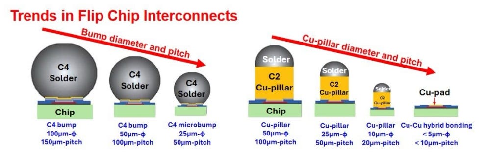
However, the latest packaging frontier—3D IC stacking—has reached thebumpless era. For instance, TSMC’s SoIC platform now implements<10 μm bump pitchconnections. This leap in packaging density brings new challenges to probe testing, as the physical footprint available for test access has virtually disappeared.
Probe Technology Strategies for Varying Interconnect Designs
To meet the demands of diverse packaging architectures, probe test strategies have evolved into three main approaches:
Schemed Cu Pad:
Targeted at larger-pitch interconnects such as traditional C4 bumps. This method designs custom copper pad patterns to improve contact stability and probe durability. It is considered a mature and widely adopted approach.
Schemed μBump:
Designed for mid-scale bump pitch (~40 μm), this approach demands precise probe card layout and controlled contact forces. It requiresadvanced alignment systemsto ensure repeatable and accurate probing across tight arrays.
Schemed Solder Pad (Test-Only):
Tailored forbumpless or sub-10 μm bump pitchscenarios, these aretest-dedicated padsintroduced temporarily and not used in final packaging. They enable electrical probing on minimal footprint areas and are indispensable in validating the reliability of ultra-dense packaging before final assembly.
Core Challenges in Ultra-Fine Pitch Probing
As bump pitch continues to shrink, probe systems face two critical challenges:
Mechanical and Positional Precision Limits:
With μBump and bumpless architectures, legacy probe modules often lack the necessary resolution. Modern probing requiresnano-level alignment accuracy, achieved via high-precision probe cards, multi-axis stage control, and laser-based visual alignment.
Advanced packaging emphasizes high-density integration and thermal reliability. The test process mustcoexist with manufacturing without compromising structural integrity. Any misalignment, over-force, or contamination during probing can degrade subsequent layers or compromise thermal/electrical characteristics. Test design must now be afully co-optimized part of the process integration flow.

2025年7月13日
TSMC’s Role and Holistic Perspective
As a global leader in advanced packaging,TSMCis not only pushing the boundaries of CoWoS and SoIC technologies but also spearheading the development ofcorresponding probe and test solutions. These include:
Advanced test-dedicated solder pad designs (Schemed μBump and bumpless)
Ultra-precision probe platform integration
Collaborations with leading test equipment suppliers to builda full high-precision probing ecosystem
TSMC’s efforts reflect a broader vision: thatchip design, fabrication, packaging, and testing must form a tightly integrated full-stack ecosystem. Only such integration enables the reliable mass production of next-generation Chiplet, 3D IC, and heterogeneous systems.
Looking Ahead
Driven by AI and HPC workloads, which demand ultra-high bandwidth and modularity, advanced packages will continue increasing the number of miniature contact points. This trajectory mandates thecontinued evolution of probing technologies—toward higher accuracy, lower mechanical stress, and higher throughput.
Far beyond being a verification step,probe testing is becoming a foundational capability—a core enabler of future semiconductor competitiveness and system-level reliability.


The New Frontier of Advanced Testing: Why TSMC Is Talking About “Thermal Challenges”
As thermal management becomes a decisive factor for advanced packaging success, the entire industry must rethink the boundaries and capabilities of testing platforms.
Driven by AI and high-performance computing (HPC), chip power density and design complexity are both skyrocketing. With technologies like CoWoS, SoIC, and chiplet integration bringing multiple dies together in extremely tight spaces, traditional test flows are now on the verge of collapse. In the past, the core question was whether the chip functioned correctly. Today, it has evolved into a more fundamental issue:can a chip be tested accurately under extreme thermal conditions?
That’s why TSMC, for the first time in its recent public presentation, dedicated a section specifically to theWafer Test Thermal Challenge. This is not just a testing issue—it’s a fundamental inflection point that affects chip yield, reliability, and mass production feasibility.
Power Density Is Rapidly Outpacing Thermal Management Capabilities
According to TSMC data, modern HPC chips are approachingpower densities of 100 W/cm², far beyond the capacity of current wafer-level test platforms. Passive cooling solutions are no longer sufficient, and even advanced active wafer-based thermal control mechanisms (like air or liquid cooling) are struggling to keep up with the thermal loads.
From a testing perspective,singulated die-based testing—while more thermally efficient—is simply not scalable for wafer-level probing, creating a critical bottleneck. The reality is clear:the higher the chip’s performance, the harder it becomes to test it using existing thermal infrastructures.
Thermal Performance: Wafer-Based vs. Singulated Die Testing
TSMC further compares the thermal response between wafer-level and singulated die-based testing:
At a power density of100 W/cm², wafer-based systems takeapproximately 40 secondsto stabilize temperature, with a ±3°C control error.
In contrast, singulated die solutions reach thermal equilibrium injust 3 seconds, with much tighter temperature control.
This discrepancy reveals a critical truth:today’s mainstream wafer test platforms are hitting a thermal efficiency wallthat jeopardizes both test accuracy and product yield for high-power SoCs.
TSMC’s Thermal Management Roadmap for Testing Platforms
For Chip Probing (CP):Thermal handling capability will improve5×from 2021 to 2025.
For Final Test (FT):Thermal performance will improvenearly 10×, enabling verification of much higher power chips.
This roadmap reflects a strategic move to incorporatethermal modeling and test-platform co-designinto its broader manufacturing optimization (DTCO) strategy.
From “Functional Validation” to “Thermal-Balanced Testing”
Chip testing is no longer just about pass/fail logic—it now must answer:
Can the chip be tested accurately under its actual thermal load?
Does the test platform have real-time thermal compensation matched to the chip’s power profile?
Are test failures due to actual defects—or caused by thermal-induced false negatives?
These questions are increasingly central to how manufacturing, testing, packaging, and system teams coordinate their engineering efforts.
Thermal Design Is the New Starting Point for Test Platform Innovation
TSMC’s focus on the Wafer Test Thermal Challenge sends a clear message:thermal constraints must now be treated as first-order factors in the design of test platforms, not merely accessories.
This marks not only a battle for equipment capability, but a signal thattest feasibility must be co-engineered from the design stage onward. As AI, chiplets, SoIC, and high-speed SerDes dominate future chip architectures, only test platforms thatsynchronize thermal, packaging, and electrical validationcan ensure continued performance scaling.
Test Challenges and Systematic Strategies in the Era of Advanced Packaging: A Full-Chain Test Approach from HBM to CPO
As AI and high-performance computing (HPC) continue to push the limits of system integration, advanced packaging technologies such as CoWoS, SoIC, and CPO are rapidly evolving. In this context,testingis no longer just a back-end verification step—it has become a critical element that spans design, manufacturing, and yield control. Especially in high-value modules like SoC + HBM, logic-integrated HBM, or silicon photonics platforms, the quality and robustness of testing strategies directly determine a product’s manufacturability and cost efficiency. This article focuses on how TSMC has extended the Known-Good Die (KGD) concept into a comprehensive system-level test architecture covering logic, memory, and photonic components.
- The Critical Role of KGD in Advanced Packaging Yield
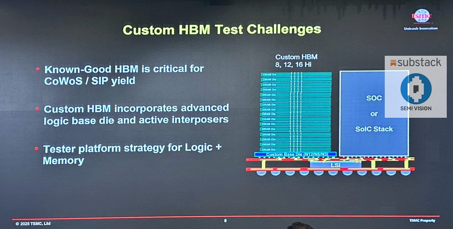
With the maturity of heterogeneous integration technologies such as CoWoS and SoIC,High Bandwidth Memory (HBM)has become essential for high-performance SoC systems. However, once an HBM stack is tightly coupled with large SoCs or chiplets through advanced packaging, any defect in a single memory die could result in thescrapping of the entire module, severely impacting yield and cost.
Therefore,pre-packaging testing of HBM must guarantee “Known-Good Die” (KGD)status—an uncompromisable requirement for high-efficiency, high-yield manufacturing using CoWoS and SoIC.
- Changing Test Requirements for Logic-Integrated HBM
In the latest packaging designs, HBM stacks are no longer simple DRAM arrays. Architectural diagrams show the integration of acustom base dieat the bottom, embedding logic control and routing functionalities using advanced logic nodes such as N12, N5, or even N3. This is closely aligned withNVIDIA’s HBM-PIM (Processing-In-Memory)concept, where memory itself performs data processing and compute functions.
Testing thesecustom HBM devicesintroduces new challenges: in addition to validating the traditional DRAM cells, the test must also verify thedigital functionality and interconnect qualityof the logic die. Thus, conventional DRAM-only testing approaches are no longer sufficient—a hybrid memory-logic validation platformis now required.
- TSMC’s Three-Stage Silicon Photonics Testing Architecture
With the integration ofsilicon photonics(SiPh) components and platforms, TSMC has established a comprehensive test flow forEICs (Electronic Integrated Circuits), PICs (Photonic Integrated Circuits), and OEs (Optical Engines). The flow is divided into three stages:
(1) EIC/PIC Bare Die Testing Stage (CP)
Independent wafer-level testing for EICs and PICs
Includes electrical validation (eSort) and optical performance verification (oSort)
Also involves top-side probe contact tests
(2) COUPE Stacked Integration Testing Stage (CP)
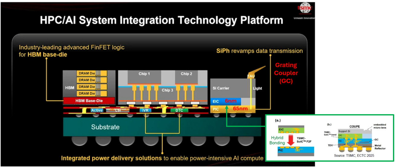
COUPE(Compact Universal Photonics Engine) is a TSMC solution integrating EIC and PIC through SoIC stacking
Key testing aspects include top and bottom probing, grating coupler (GC) and edge coupler (EC) alignment and insertion loss verification
Ensures electrical-optical inter-die connectivity and mechanical alignment
(3) CPO Final Package and Functional Test Stage (FT)
Post-packagingCPO (Co-Packaged Optics)testing validates full-module functionality
Test platforms must support CoW (Chip-on-Wafer) based systems, covering optical I/O paths, ASIC data transmission, and thermal control validation
- Enabling Techniques for Complex Heterogeneous Testing
To handle the growing complexity in optoelectronic integration, TSMC employs several key test technologies:
Probe card + fiber array co-testing: Enables parallel wafer-level testing of both electrical and optical signals, reducing cycle time and improving throughput
Grating Coupler Testing: Uses silicon interposer and micro Si lens for vertical optical injection; common during PIC test stages
Edge Coupler Testing: Employs horizontal fiber coupling into SiN waveguides; used to validate optical I/O at the module level
These methods collectively supportdie-level, stack-level, and system-level validation, forming the backbone for future CPO mass production workflows.
Testing as a Core Part of the Manufacturing Platform
Historically, testing was seen as the final quality control checkpoint in the semiconductor manufacturing process. Today, with the rise ofchiplets, custom HBM, silicon photonics, and CPO platforms, testing is no longer just about verification—it has become anextension of design, process, and system reliability engineering.
TSMC’s full-chain test strategy demonstrates its deep understanding and comprehensive roadmap for heterogeneous integration. It signals an industry-wide shift toward a new era where“testing is a platform capability,” not an afterthought. In this future, only companies that treat test infrastructure as an integral part of system architecture will be able to keep pace with the demands of the AI and HPC era.
Four Key Challenges and Technical Barriers in Mass Production Testing of Silicon Photonics (SiPh)

With the rapid rise of AI and high-bandwidth communication demands,Silicon Photonics (SiPh)is increasingly seen as a critical enabler for next-generation high-speed interconnects and data processing. However, for SiPh to truly achieve scalable mass production, it must overcome a core obstacle:testing. Unlike traditional electrical components, SiPh involves optoelectronic hybrid structures and precise alignment requirements, posing significantly higher technical demands on test platforms. This article outlines the four major challenges in SiPh production testing and the associated technological bottlenecks and solution paths.
- FAU Alignment Precision
Challenge: TheFiber Array Unit (FAU)is a critical interface for optical signal coupling between fibers and SiPh dies. It must be aligned atnanometer-scale accuracyto minimize optical coupling loss.
Technical Barrier: Current alignment procedures require extensive time to optimize optical power. While this is acceptable for single-die testing, in high-volume manufacturing scenarios involving thousands of dies, alignment time becomes the primary bottleneck—directly impacting yield and throughput.
- Anti-Vibration Stability
Challenge: SiPh testing relies heavily on the stability of optical spectrum and power. However, micro-vibrations from test platforms, environmental factors, or even building infrastructure can cause measurement fluctuations, leading toinconsistent test results(ripple effects).
Technical Barrier: While active suspension or vibration isolation platforms can mitigate this issue, theysignificantly increase equipment costand require larger footprints and more complex maintenance. Achieving the right balance between cost, stability, and measurement consistency is a core challenge in test platform design.
- CPO Package Test Automation
Challenge:Co-Packaged Optics (CPO)integrates multiple Optical Engines (OEs) and ASICs into complex packaging structures. Testing must coveroptical coupling, electrical functionality, and thermal behaviorin a multidimensional manner.
Technical Barrier: Automation of CPO testing requires integration of:
High-precision FAU alignment systems
Multi-axis motion controllers with automated fiber array movement
Electrical probe card interfaces
These fully integrated test systems are still under development and validation, makingCPO production yield and test cost optimizationhighly challenging at present.
- Double-Sided Probing Architecture
Challenge:COUPE (Compact Universal Photonics Engine)is a vertically stacked integration of EIC (Electronic Integrated Circuit) and PIC (Photonic Integrated Circuit) using SoIC technology, requiringsimultaneous top and bottom probingfor electrical and optical signal validation.
Technical Barrier: Conventional probe platforms only support single-sided probing. For COUPE, a newdouble-sided probing systemis needed, integrating:
Top-side optical alignment and FAU docking
Bottom-side electrical probe card or test socket
Structural stability and thermal management mechanisms
This introduces multiple challenges across platform mechanics, material selection, thermal interference control, and software coordination.
TSMC’s Strategic Approach to Silicon Photonics Testing
These four challenges clearly demonstrate thatSiPh testing involves far higher technical thresholdsthan conventional semiconductor processes. As a global leader in advanced packaging and heterogeneous integration,TSMCis actively investing in the development and deployment of key testing technologies across:
FAU alignment automation
Anti-vibration testing platforms
CPO test automation systems
Double-sided probing solutions for COUPE architectures
By integrating electrical probe cards with optical test systems,TSMC is building a complete, high-throughput, low-cost, and scalable test infrastructurethat supports COUPE, CPO, and SiPh devices. This lays a solid foundation for the future of AI datacenters and high-speed communication infrastructure.
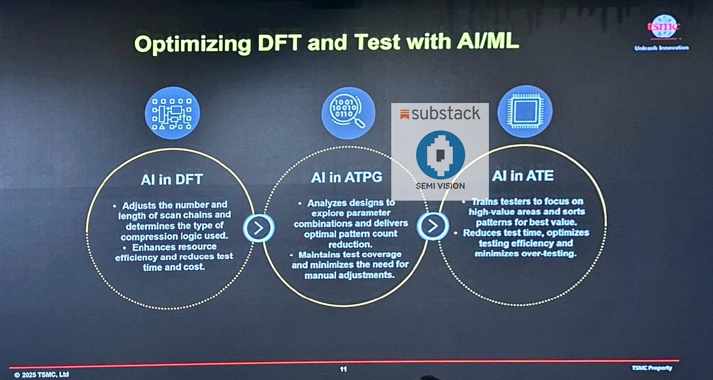
AI/ML-Driven DFT and Test Optimization: Ushering in the Intelligent Era of Semiconductor Testing
- AI in Design-for-Test (DFT)
During the DFT phase, AI can automatically analyze circuit structures to optimize test observability and controllability, particularly in the following areas:
Scan Chain Optimization:
AI automatically determines the number and length of scan chains, preventing unnecessary logic congestion and redundant scan regions, enabling a more compact design layout.
Compression Architecture Selection:
AI models can intelligently select the most suitable test compression techniques (e.g., EDT, XpressComp) based on design characteristics and target test coverage.
Benefits:
This improves resource utilization, reduces test time and equipment costs, and is especially beneficial for area-sensitive or low-power designs.
- AI in ATPG (Automatic Test Pattern Generation)
ATPG is critical for generating test vectors that cover potential fault modes. AI further enhances its efficiency through:
Parameter Exploration:
AI can analyze circuit logic and path distributions to automatically explore optimal parameter combinations, improving pattern generation quality.
Test Vector Minimization:
AI helps minimize redundant vectors while maintaining high fault coverage, reducing the overall number of patterns.
Benefits:
By minimizing manual tuning and accelerating vector generation, test load time and total cost can be significantly reduced.
- AI in ATE (Automated Test Equipment)
In the physical testing phase, AI enhances decision-making based on real-time measurement data:
Targeted Test Focus:
Using trained models, the test system can identify high-risk areas and prioritize testing accordingly, improving test ROI.
Test Pattern Reordering and Trimming:
AI leverages historical data and efficiency predictions to adjust the order or remove low-value test patterns, avoiding over-testing.
Benefits:
This shortens on-chip test time and boosts ATE utilization, particularly for complex multi-die or heterogeneous integration systems.
AI-Driven End-to-End Test Chain Transformation
AI/ML technologies are driving semiconductor testing into anew era of intelligence and autonomy. From design (DFT), pattern generation (ATPG), to physical execution (ATE), every step is now being optimized and connected through AI, forming a cohesiveend-to-end intelligent test chain. This not only reduces development and production cycles but also boosts yield and cost efficiency—an essential advantage for today’s rapidly evolving SoC and chiplet systems.
As advanced packaging, AI accelerators, and hyperscale datacenter deployments become increasingly prevalent,AI is no longer merely a design aid, but is poised to becomethe central engine of semiconductor test performance and reliability.

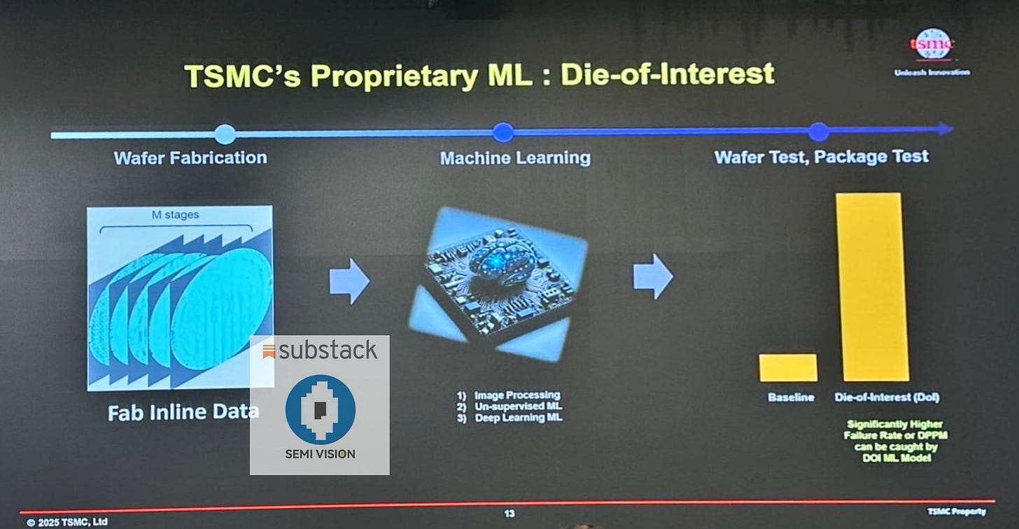
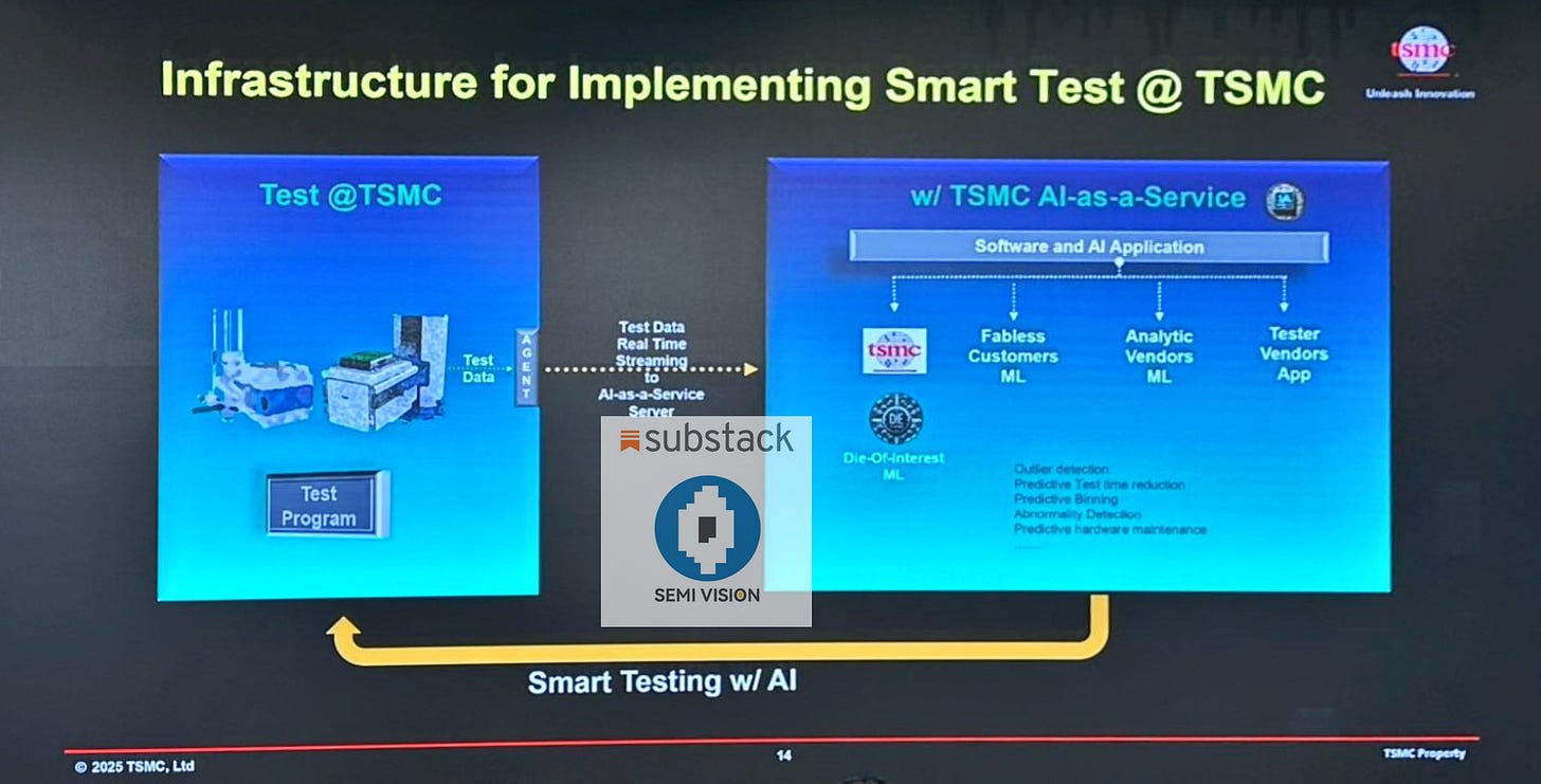
AI/ML-Driven DFT and Test Optimization: Ushering in the Intelligent Era of Semiconductor Testing
As chip design complexity continues to soar—especially in large-scale SoCs, AI accelerators, and chiplet-based systems—traditional design and testing methodologies are reaching their limits in efficiency and cost. Against this backdrop, artificial intelligence and machine learning (AI/ML) technologies are being introduced into Design-for-Test (DFT) and testing workflows, enabling a new era of “intelligent test optimization.” This transformation not only accelerates design-to-production cycles but also significantly reduces testing costs and reliance on human resources, becoming an essential capability in advanced semiconductor manufacturing.
- AI in DFT (Design-for-Test)
In the DFT phase, AI can automatically analyze circuit structures to optimize observability and controllability. This manifests in two key areas:
Scan Chain Optimization: AI determines the optimal number and length of scan chains, avoiding unnecessary congestion or redundant scan regions, and enabling a more compact layout.
Compression Architecture Selection: AI models can automatically select the most appropriate test compression techniques and architectures (e.g., EDT, XPressComp) based on design characteristics and target coverage rates.
Impact: Enhances resource efficiency, reduces back-end test time and tester cost—especially beneficial for area- and power-sensitive designs.
- AI in ATPG (Automatic Test Pattern Generation)
ATPG generates patterns to detect potential faults. AI significantly boosts this process by:
Parameter Exploration: AI analyzes logic structures and path distributions to search for optimal parameter configurations that improve pattern generation speed and quality.
Pattern Minimization: AI helps eliminate redundant patterns while maintaining high fault coverage, reducing total vector count.
Impact: Reduces manual tuning, accelerates test vector generation, cuts load times, and lowers overall test cost.
- AI in ATE (Automatic Test Equipment)
During physical chip testing, AI enables dynamic decision-making by:
Risk-Based Prioritization: AI models identify high-risk regions to prioritize test coverage for maximum return on test investment.
Test Mode Pruning and Reordering: AI adjusts test sequences and eliminates low-value test modes, avoiding over-testing.
Impact: Shortens test time, increases tester utilization, and proves especially effective in multi-chip or heterogenous systems.
Intelligent End-to-End Testing Workflow
With AI/ML integration, semiconductor testing is transitioning toward a fully intelligent and autonomous workflow. From DFT to ATPG to ATE, each stage’s data and decisions are AI-optimized, forming an “end-to-end intelligent test chain.” This not only compresses design cycles and time-to-market but also improves test yield and cost efficiency, providing a decisive advantage in the face of rapidly evolving SoCs and chiplet-based systems.
In a world increasingly driven by advanced packaging, AI accelerators, and data center deployments, AI is no longer just a design aid—it is becoming the driving force behind semiconductor test productivity and reliability.
Challenges in AI Chip Testing
AI accelerator chips often feature extreme power density and highly complex architectures. These characteristics create numerous testing challenges:
High Pin Count and Signal Complexity: AI chips may integrate billions of transistors across multi-core architectures operating at varied frequencies. As die sizes increase, so does pin count—today’s 150 mm² chips can have 22,000 pins, potentially growing to 80,000. This causes signal integrity issues, probe contact failures, and crosstalk.
Thermal Management in Probing: The high power dissipation during tests generates significant heat. If not properly controlled, probes or even the chip itself may be damaged. Companies like FormFactor emphasize precision thermal control and advanced probe cards to prevent thermal drift or component failure during probing.
Interconnect Density and Probe Precision: AI chips using 2.5D/3D packaging and micro-bump or TSV interconnects require extremely accurate probing. Micro-bumps as small as 25 µm with 45 µm pitch demand sub-micron positioning. MEMS hybrid probes capable of 1A per pin and adaptive Z-axis compensation are necessary.
Test Time and Coverage: Traditional functional testing is time-consuming for such large logic volumes. AI chip testing must employ BIST, hardware acceleration, and parallel high-speed testing platforms (e.g., TEL Precio XL, FormFactor Apollo) to meet throughput demands.
HBM Memory Testing Challenges
High Bandwidth Memory (HBM) employs stacked DRAM dies with TSV interconnects. For custom HBM (cHBM), a logic base die (often customer-designed) is integrated, further complicating testing.
Known-Good Die (KGD) Testing: Each die must be verified pre-stack to avoid yield loss. As stack layers increase from 4 to 16, wafer-level testing becomes critical. FormFactor’s HFTAP K40 probe cards support over 7GHz testing with low insertion loss, advanced flatness control, and thermal expansion compensation.
Logic + Memory Co-Test: The base die often includes memory controllers and BIST, requiring both memory and logic to be validated together. Testing must ensure interconnect integrity and logic correctness under full stack thermal/mechanical stress.
Tiered Testing Workflow:
Wafer-Level Testing: Initial defect screening and KGD validation.
Pre-Packaging Test: Speed binning and functional sorting using test carriers.
Post-Packaging Module Test: Full-system performance and reliability checks.
Probe cards like FormFactor’s HFTAP Matrix and precise thermal control are essential to avoid yield-damaging escapes.
CPO, PIC, EIC, and Optical Engine Testing
Co-Packaged Optics (CPO) integrates PIC and EIC into a single package, creating new test demands across stages:
Wafer-Level Test: Dual-sided test platforms (e.g., ficonTEC + Teradyne) conduct top-side electrical and bottom-side optical alignment. These platforms support vacuum thermal chucks, 6-axis active fiber alignment, and auto-PIC mapping, all compatible with standard ATEs (e.g., Advantest V93000 + FormFactor Velox).
Die-Level Test and Assembly: After dicing, PIC and EIC dies undergo automated alignment and testing. FiconTEC’s automation handles horizontal/vertical coupling, optical/electrical co-testing, and FAU bonding, ensuring sub-0.1 dB repeatability.
Module-Level Test: Final test of fully integrated optical engines includes bandwidth, power, and reliability checks. FormFactor’s TRITON platform supports both edge and grating couplers and integrates optical/electrical measurement in one flow.
Each stage must ensure sub-micron alignment, vibration control, and simultaneous EO (electrical-optical) evaluation.
Test Equipment Vendors and Market Opportunities
TEL (Tokyo Electron): Provides high-precision wafer probers (e.g., Precio series) with multi-DUT support and thermal vibration control. Ideal for large AI chips and high-pin-count packages. As die sizes and integration rise, TEL’s platforms will grow in relevance.
Advantest: Market leader in memory and SoC testing. HBM test revenue represents ~50% of its memory business and is expanding due to AI growth. V93000 and UltraFLEX platforms serve HBM and SoC markets. Advantest is expanding into silicon photonics via partnerships (e.g., with FormFactor and ficonTEC).
FormFactor: Renowned for wafer probe cards. Apollo (up to 30k pins, 1A per pin), HFTAP (HBM-focused), and TRITON (EO testing) form a robust product line. Adopted by over 100 silicon photonics customers worldwide.
FiconTEC: Specializes in photonic device automation. Its full-stack solutions—from wafer to module—include FAU bonding, UV cure, thermal compression, and EO metrology. Their “lab-to-HVM” product line is ideal for growing CPO/AI optical needs.
AI computing, memory architectures, and photonic packaging are redefining the test equipment landscape. Advantest and FormFactor are leveraging collaboration to capture photonics and memory test growth, TEL and MPI anchor wafer-side hardware, and FiconTEC leads photonic assembly and testing. In a future shaped by high integration and high-frequency challenges, all these vendors are poised to grow market share and technological leadership.


PreviousNext
TopLatestDiscussions








See all