Decoding Node Strategy: MediaTek’s Long-Lasting Process Nodes and AI Roadmap
Decoding Node Strategy: MediaTek’s Long-Lasting Process Nodes and AI Roadmap
- Source: SemiVision
- Author: SEMIVISION
- Published: 2025-07-15T09:24:38+08:00
- URL: https://tspasemiconductor.substack.com/p/decoding-node-strategy-mediateks Decoding Node Strategy: MediaTek’s Long-Lasting Process Nodes and AI Roadmap


Decoding Node Strategy: MediaTek’s Long-Lasting Process Nodes and AI Roadmap
Original Articles By SemiVision Research (MediaTek , TSMC , Nvidia , AWS , Google , Ranovus , Alphawave Semi ,Xanadu , AMD , Cerebras )

Jul 15, 2025
∙ Paid
From Chip Definition to System Integration: MediaTek at the Crossroads of Advanced Packaging
In the era of AI-driven performance-per-watt optimization and heterogeneous integration, the nature of chip design is shifting—from a singular focus on computational horsepower to a packaging-centric, system-level co-design paradigm. Under the traditional Moore’s Law trajectory, the interplay between performance, power, and cost (PPC) is increasingly challenged beyond the 7nm node. While advanced nodes still offer advantages for specific applications, escalating manufacturing costs, slower SRAM scaling, and diminishing cost-per-transistor improvements are forcing the industry to seek new performance uplift curves. Advanced packaging has emerged as the key enabler to transcend the limitations of traditional node scaling.

2025年5月21日
As a global leader in IC design, MediaTek has evolved from its consumer electronics SoC roots to expand into Edge AI, ASICs, and automotive markets. In doing so, it has increasingly recognized advanced packaging not merely as a manufacturing consideration, but as a strategic capability. This evolution touches not only how chips are architected and IPs are integrated, but how system-level synergy across performance, thermal design, and power consumption can be fully optimized.
Extension|MediaTek’s Advanced Packaging Strategy Through the Lens of ASIC Evolution

As MediaTek enters the ASIC domain, its role shifts from a provider of high-integration SoCs to a collaborative development partner for application-specific and vertically integrated solutions. In AI servers, voice assistants, and edge computing, MediaTek co-creates highly customized designs with clients—driving up the demand for packaging technologies that enable flexibility, integration, and reliability.
Unlike traditional consumer-grade chips that chase economies of scale, ASICs and Edge AI emphasize packaging flexibility and modularity. As such, MediaTek is focusing on several key packaging trends:
2.5D/3.5D Heterogeneous Integration: Leveraging architectures such as CoWoS-L and CoWoS-R to integrate AI accelerators, SerDes, and HBM onto a single packaging platform;
Yield-Driven Packaging Selection: Choosing long-tail nodes and mature packaging (e.g., organic substrates with embedded silicon bridges like EMIB) to manage BOM costs and reduce ramp-up complexity;
Adoption of Glass Core Substrates: For applications requiring superior warpage control and electrical performance, glass substrates are emerging as a transformative next-generation option.
In summary, as MediaTek advances into the ASIC and high-end Edge AI domains, it is no longer just a traditional chip vendor. It is becoming a system integrator, using advanced packaging as a strategic platform to meet new expectations in AI, connectivity, and automotive markets. With increasing demand for energy efficiency and modular scalability, advanced packaging is poised to be a key differentiator and a gateway for MediaTek’s entry into high-value markets.

From Smartphones to AI Chip Design Services: MediaTek’s Strategic Shift and Process Technology Strategy
At the 2025 IEEE VLSI Symposium panel discussion, MediaTek clearly articulated its transformation from a consumer SoC provider to a critical solution partner in the AI era. The discussion revealed that MediaTek is no longer confined to smartphone APs and voice assistant platforms—it is now actively providing SerDes IP and offering design services for cloud service providers (CSPs) developing AI chips, marking a pivotal step in its evolution.
This article begins by examining MediaTek’s transformation and delves into its logic process technology strategy, evolving ASIC design philosophy, and long-term vision for advanced packaging.
- MediaTek’s Transformation: From SoC Supplier to AI Chip Partner
Over the past decade, MediaTek has built strong SoC integration capabilities across smartphones, TVs, and IoT markets. In the AI era, the company has shifted toward AI-centric chip design, particularly in voice assistants, edge AI, and AI accelerators—offering customized, system-oriented solutions.
A key milestone in this transformation is MediaTek’s growing investment in high-speed SerDes IP. Originally developed for internal SoC interconnects, SerDes capabilities are now supporting CSP clients in high-performance AI training chips, enabling fast interconnects with HBM, switch chips, and other components. This has become a critical foundation for MediaTek’s AI chip design services.
- Logic Process Strategy: Balancing Advanced and Mature Nodes
At the panel, MediaTek emphasized the importance of flexible process node selection, stating that different application scenarios require different co-optimization approaches under its in-house DTCO framework (Design-Technology Co-Optimization):
For high-performance AI training/inference chips, MediaTek evaluates nodes like TSMC N3 or N2 based on transistor density, power efficiency, and compatibility with SerDes voltage requirements. While GAA offers better drive current, its high cost and design complexity must be carefully assessed.
This “application-driven process selection” signals a fundamental shift from performance-centric SoC thinking to a system-level integration mindset.
- A Packaging-Centric Approach: From Chip Modules to System Platforms
As chip performance becomes increasingly constrained by interconnects and packaging, MediaTek is actively developing integration strategies focused on advanced packaging technologies. Its key approaches include:
2.5D integration (e.g., CoWoS-L): For high-performance AI ASICs that require HBM and multi-die logic integration.
EMIB bridging: Combining mature-node logic designs with high-speed SerDes to achieve cost-effective, high-bandwidth packaging.
RDL modular packaging: Supporting flexible IP configurations and promoting the concept of “package as system.”
Adoption of glass core substrates: Addressing needs for warpage control and electrical performance—particularly relevant for automotive AI and high-speed communication ASICs.
Furthermore, MediaTek highlights that DTCO and STCO (System-Technology Co-Optimization) are critical to future adoption of 3D ICs and chiplet architectures.
- From Smartphone-Driven SoCs to Packaging-Defined AI Platforms
MediaTek now stands at the intersection of logic design, system packaging, and IP integration. Its role is evolving from a chip supplier to a packaging-centric system design partner. This transformation enables MediaTek to carve out a differentiated position in the increasingly competitive markets of AI ASICs and Edge AI solutions.

As CSPs, automotive OEMs, and next-generation manufacturing industries demand higher energy efficiency, bandwidth, and modularity, MediaTek’s continued progress in packaging architectures, process co-design, and IP collaboration will determine its long-term value in the AI infrastructure landscape.
In the AI-driven wave sweeping across the semiconductor industry,MediaTekis no longer just the silent champion of mobile SoCs—it is emerging as a key enabler powering voice assistants, smart homes, AI tablets, and intelligent edge devices. While much of the industry remains fixated on cloud-scale model training and hyperscale compute, MediaTek is quietly building a device-centric AI empire through ASIC development, advanced packaging, and long-lifecycle process node strategies.
From PoP memory architectures to 2.5D/3D heterogeneous integration, from ultra-low-power neural inference for voice agents to its strategic use of TSMC’s N3E as a long-lasting node in the GAA era—every step MediaTek takes is not merely a technical decision, but a calculated balance of design flexibility, cost optimization, and system efficiency.

2025年7月10日
In the evolving global semiconductor innovation landscape, Canada is increasingly showcasing its technological potential and industrial competitiveness. Beyond its long-standing foundation in quantum computing and photonics research, recent years have seen a surge of startups actively engaging in Silicon Photonics, Advanced Packaging, Co-Packaged Optics (CPO), custom AI ASICs, and Lithium Niobate on Insulator (TFLN) technologies. These developments are gradually shaping a regionally distinct semiconductor innovation ecosystem in Canada.

Among them,Ranovusstands out as a prominent player. Headquartered in Ottawa, the company specializes in modular CPO optical engines and EPIC (Electronic-Photonic Integrated Circuit) platforms. Ranovus has already established partnerships with leading global semiconductor companies such as AMD, Cerebras, and MediaTek. Its Odin® optical engine, now in mass production, supports high-speed DWDM transmission and offers advantages in low power consumption and high integration. Ranovus is one of the few startups globally to have successfully entered the commercial deployment phase of CPO technology.

Alphawave Semi, formerly known as Alphawave IP and also based in Toronto, has gradually evolved into a publicly listed company. It originated in the fields ofSerDes,optical interconnects, andcustom ASIC architectures, and continues to develop advanced packaging solutions supportingUCIe,CXL, andchiplet-based system integrationthrough its Canadian R&D center.
Additionally, companies likeXanadu, which focus onoptical quantum computing, are pushing boundaries. While primarily centered on quantum information, Xanadu’s silicon photonics platform and fabrication technologies are increasingly converging with the broader semiconductor supply chain, particularly inTFLN materialsandhybrid bondinginnovations.
In summary, Canadian semiconductor startups are emerging as key innovators, leveraging core themes such as photonics-electronics convergence, high-bandwidth interconnects, CMOS-compatible processes, and heterogeneous integration to tap into next-generation global semiconductor competition. This growing ecosystem is one that should not be overlooked.

2025年7月11日
MediaTek Partners with Ranovus: Advancing into the High-Performance AI Chip Era with Co-Packaged Optics (CPO)
As AI and HPC workloads scale exponentially,bandwidth and power efficiencyhave emerged as the primary bottlenecks in expanding system architectures. To strengthen its system integration capabilities in AI ASIC design,MediaTekannounced a strategic partnership in 2024 with Canadian photonics companyRanovus. Together, they aim to co-develop next-generationCo-Packaged Optics (CPO)solutions, injecting high-efficiency optical interconnect technologies into future AI chip platforms.
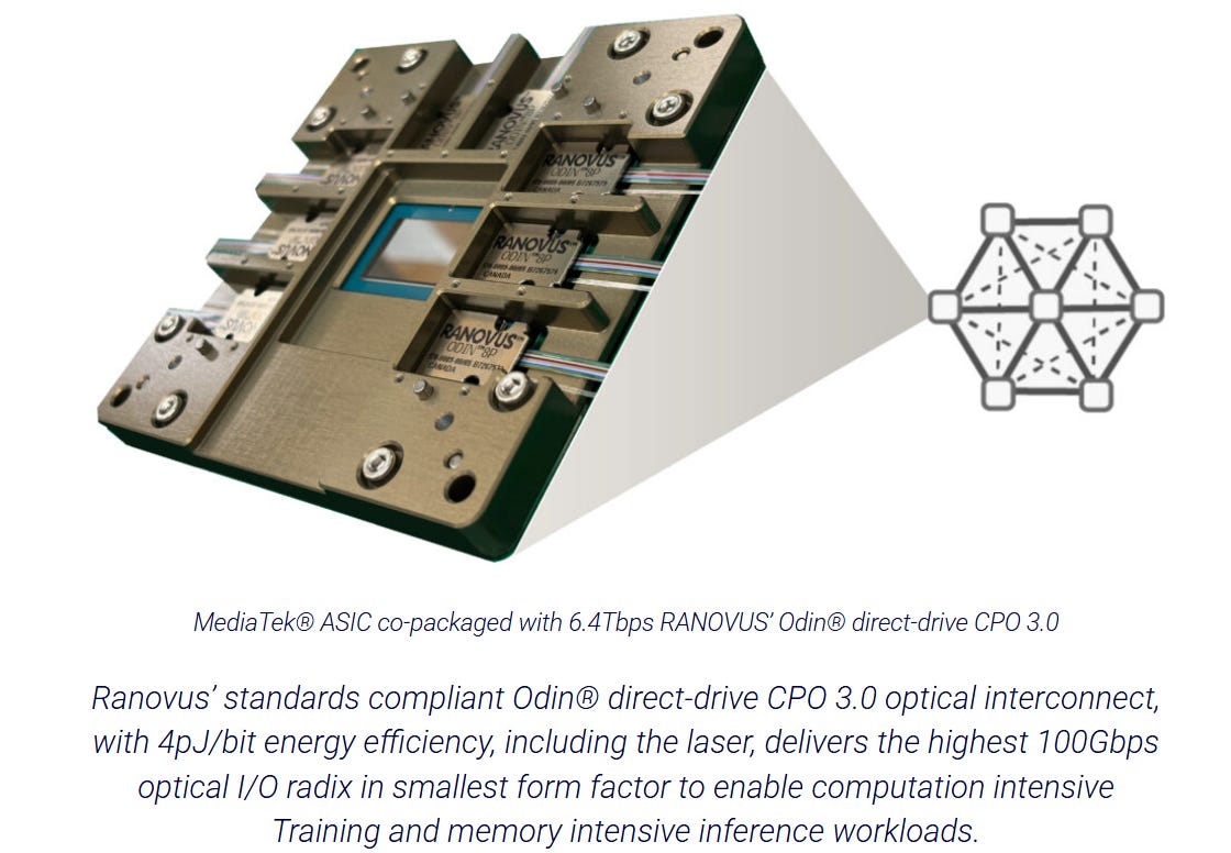
A Modular CPO Platform: System Design Breakthrough by MediaTek × Ranovus

MediaTek’s new-generation ASIC design platform integrates its proprietary112Gbps SerDes technologywith Ranovus’Odin® optical engine, achieving a highly modular electro-optical integration. This platform supports8×800Gbps electrical and optical channels, featuring low power consumption, high bandwidth, modularity, and reconfigurability. Not only does this significantly reduce PCB routing complexity and packaging footprint, but it also cuts overall system power consumption by up to50%, providing an economically viable high-speed interconnect solution for AI data centers and large-scale inference systems.
This collaboration marks MediaTek’s strategic transition from mobile SoC design towarddata center-class AI platforms, pushing its chip design and packaging integration capabilities to meet next-generation bandwidth and energy efficiency demands.
Ranovus: A Pioneer in AI Optical Interconnects
Ranovus, headquartered in Ottawa, Canada, is a leading player in optical interconnect solutions. The company offers a comprehensive platform includingQuantum Dot Lasers, integratedElectronic-Photonic Integrated Circuits (EPIC), and high-densityCPO modules. ItsOdin® seriesdelivers power efficiency as low as4pJ/bitand supports over6.4Tbps of bandwidth, making it one of the most advanced CPO modules in the industry.
Ranovus’ core strength lies in itshigh level of integration,production-ready design, andclose ties with global foundry and packaging supply chains, enabling it to rapidly support system vendors in building commercial-grade CPO platforms.
Collaborations with AMD, MediaTek, and Cerebras
In addition to MediaTek,Ranovus has formed strategic partnerships with several leading semiconductor companies:
AMD/Xilinx: Ranovus previously demonstrated itsOdin 2.0platform integrated into AMD’s FPGAs and AI acceleration chips, targeting AI/ML edge computing applications.
Cerebras Systems: In 2025, Ranovus and AI chipmaker Cerebras jointly secured aDARPA contractto implement optical interconnects into Cerebras’ wafer-scale systems, supporting ultra-large-scale AI training.
These collaborations underscore Ranovus’ role as a core enabler ofcross-platform, cross-application optical interconnect deployment, with proven technical versatility and execution.
MediaTek’s Strategic Intent Behind CPO
For MediaTek, the partnership with Ranovus carries three strategic implications:
Rapid Entry into the High-Bandwidth Interconnect Market: Leveraging Ranovus’ mature platform, MediaTek can quickly build CPO module development and validation capabilities.
Enhancing the Completeness of its AI ASIC Platform: MediaTek moves beyond providing compute cores to offering afully integrated solutionencompassing IO, SerDes, optical modules, and packaging.
Alignment with High-End Supply Chain Players: Co-development with Ranovus andTSMCstrengthens MediaTek’s influence in advanced packaging and system-level integration.
TheMediaTek–Ranovus partnershipis more than just a technical alliance—it signals theentry of Taiwanese IC design houses into the core battlefield of high-bandwidth, low-power AI/HPC data center platforms. As AI models continue to grow in scale andCPO becomes central to future system architectures, MediaTek’s bold move is poised to fuel itsnext phase of growthacross data centers, cloud infrastructure, and AI chip markets.
In thisSemiVision Technical Special, we unpackseven strategic pillarsof MediaTek’s platform play—spanning FinFET-to-GAA packaging transitions, SRAM bottleneck solutions, edge AI SoC architecture, and how N3E has become the modern definition of a long-lifecycle node. Each topic dives deep not only into the underlying technologies but also the broader system-level logic and supply chain implications.
If you care about the evolution of edge devices in the AI era, therealvalue of advanced process nodes like N3E, or are looking to differentiate through packaging and heterogeneous integration—this is the article you cannot afford to miss.
Unlock the full story and discover how MediaTek is quietly becoming the most strategic “system player” in the AI age.
For Paid Members , SemiVision will discuss topics on
The Long-Term Evolution of Process Nodes: Key Inflection Points Behind Each Generational Leap
The Four Driving Forces Behind Technological Leaps: Materials, Lithography, Patterning, and Device Architecture
Platform Nodes and System-Level Integration: The Decision Matrix for IC Design Houses
Strategic View: Process Evolution as a Platform-Driven Race
The Node You Choose Is the Platform You Build On
From Node Scaling to Platform Strategy: The Logic of Long-Lived Nodes and the Strategic Role of TSMC N3
N3: TSMC’s Modern Definition of a Long-Lived Node
Process Scaling Is Guided by a Rhythm of Long-Lived Nodes
The Concept of the “Process Universal Curve”
The Evolutionary Trend of Advanced Process Nodes in Performance and Power — The “PP” in PPA
Area Scaling Trends in Advanced Process Nodes: The Bottleneck of SRAM Miniaturization
Transistor Cost Reduction in Advanced Nodes: Slowing Down and Facing Reversal at 2nm and Beyond
The Bottlenecks and Transformation of Moore’s Law in the Sub-7nm Era
MediaTek Joins Forces with Google: Strategic Entry into TPU Design and Its Future Implications
2.5D and 3.5D Advanced Packaging Architectures: Comparing TSMC’s CoWoS and Intel’s EMIB
Future Scalability of CoWoS and EMIB in Heterogeneous Integration Packaging
A Critical Inflection Point in Core Substrate Materials for Advanced Packaging
Scaling Advanced Packaging: Multidimensional Challenges and the Rise of Glass Substrates
SemiVision Technical Insight Series: Unpacking MediaTek’s Innovation Across Seven Strategic Dimensions
1.MediaTek’s Strategy and Challenges in Advanced Packaging: CoWoS, EMIB, CPO, and Glass Substrates
2.Collaboration Between MediaTek and NVIDIA on AI ASIC and NVLink Technologies
3.Differentiating Products Through Advanced Packaging: MediaTek’s Path into Cloud AI and HPC
4.Automotive Market Strategy: 3nm DX1 Platform, 5G Cockpit Integration, and Packaging Challenges
-
Edge AI Product Line: GB10 and Multi-Agent (MCP/A2A) Architecture Enabled by Advanced Packaging
-
Packaging Challenges and Solutions in the FinFET/GAA Era: PPA Optimization, SRAM Bottlenecks, and Cost Control
-
End Applications: Voice Assistants, Smart Home, and AI Tablet Strategy — Empowered by Advanced Packaging and AI ASIC Integration
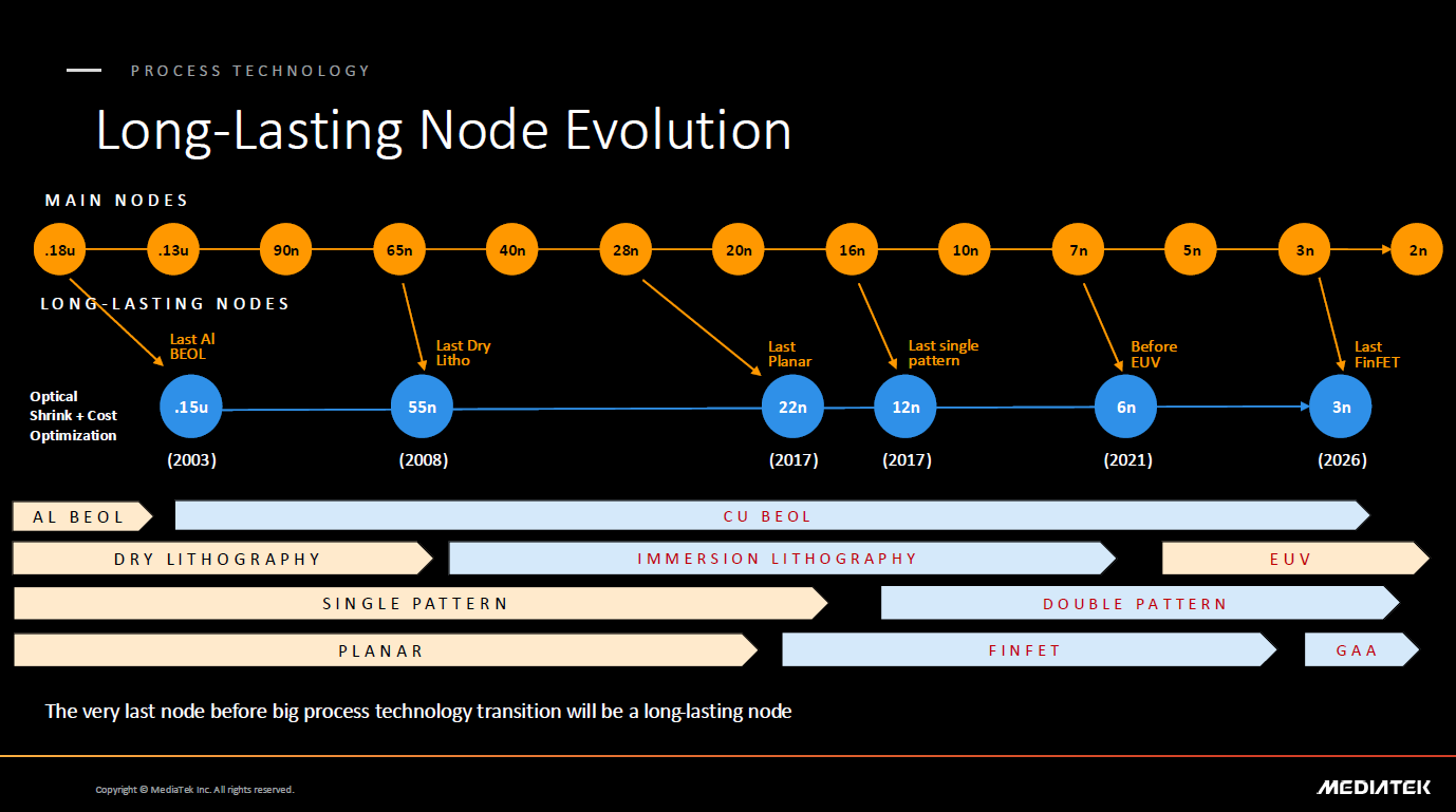
The Long-Term Evolution of Process Nodes: Key Inflection Points Behind Each Generational Leap
Starting from the early days of the 0.18-micron node, the semiconductor industry has continuously advanced through optical scaling and cost optimization—progressing through 0.13 µm, 90 nm, 65 nm, and into today’s cutting-edge 3 nm and even 2 nm era.
Throughout this journey, certain nodes have emerged as“long-lasting nodes”, playing critical roles in enabling industry transitions. For example:
0.15 µm (2003)marked the last node usingaluminum (Al) back-end-of-line (BEOL)interconnects;
55 nm (2008)represented the final node relying ondry lithography;
22 nmwas the last node usingplanar transistor architecture;
12 nmbecame the last node based onsingle-patterning lithography.
Due to their process stability and cost-effectiveness, these nodes have been widely adopted in mainstream and legacy applications, continuing to serve a broad range of markets even years after their introduction.
Entering the sub-10 nm regime, the industry witnessed a steep rise in process complexity with the adoption ofEUV (Extreme Ultraviolet) lithographyand the widespread deployment ofFinFET (Fin Field-Effect Transistor) architectures. The7 nmnode is widely regarded as the final pre-EUV generation, while3 nmrepresents the last of the FinFET era, paving the way for the next paradigm:GAA (Gate-All-Around) transistors.
This evolutionary path highlights key shifts in technology:
Materials: Transition from aluminum to copper interconnects;
Lithography: Migration from dry to immersion and then to EUV;
Patterning: From single to double patterning and multi-patterning techniques;
Device structures: From planar transistors to 3D architectures like FinFET and GAA.
A crucial takeaway is that each major transition in process technology has been preceded by a“long-lasting node”—a node that provides manufacturing stability and cost support during periods of architectural change. This indicates that process advancement is not linear but rather a strategic evolution shaped by platform maturity and technological barriers.
For IC design companies likeMediaTek, these insights offer strategic value when selecting process nodes—balancing performance, yield, and market timing to maximize commercial viability.
The Four Driving Forces Behind Technological Leaps: Materials, Lithography, Patterning, and Device Architecture
Every major node transition in semiconductor history has been driven by breakthroughs in four core areas:
Material Transition: From aluminum to copper interconnects, from low-k to ultra-low-k dielectrics, and now to emerging conductors such as ruthenium.
Lithography Advancement: From dry lithography to 193nm immersion, and onward into the era of EUV (Extreme Ultraviolet) lithography.
Patterning Techniques: Evolving from single patterning to complex multi-patterning flows such as SADP, LELE, and LELELE.
Device Structure Evolution: From planar transistors to FinFETs and now to Gate-All-Around (GAA), striking an optimal balance between drive strength, density, and power.
Among these milestones,7nmis often regarded as the peak of pre-EUV scaling, while3nmmarks the final chapter of the FinFET era. The transition to2nmbrings GAA architecture into the spotlight, ushering in a new era of transistor design.
Platform Nodes and System-Level Integration: The Decision Matrix for IC Design Houses
For fabless design companies likeMediaTek, Qualcomm, and NVIDIA, each process node is more than just a technical consideration—it is astrategic business decision. Key trade-offs include:
Performance vs. Cost: While leading-edge nodes offer greater transistor density and performance, they also come with skyrocketing design and fabrication costs—not every application can justify the investment.
Yield vs. Time-to-Market: Mature nodes offer higher production yields and predictable schedules, making them ideal for markets with stable demand and tight development timelines.
Packaging Co-Design: Advanced packaging technologies (e.g., CoWoS, InFO, EMIB) are increasingly essential to overcoming node limitations. In many cases, a “node + packaging + IP integration” strategy offers more commercial value than simply chasing the latest node.
Strategic View: Process Evolution as a Platform-Driven Race
From an industry perspective, the rise of “long-lasting nodes” reflects a broader negotiation between technological ambition and manufacturing reality. These nodes are not just technical thresholds—they areplatforms. Their common traits include:
High Return on Investment (ROI): Tools and IPs are reusable across multiple generations.
Standardized Manufacturing Ecosystem: Mature equipment (EPI, furnaces, CMP, test platforms) is widely available and optimized.
Stable Design Rules: EDA validation and yield models are refined over hundreds of tapeouts.
Robust IP Library: Including mainstream blocks such as SRAM, SerDes, ADC, RF, and more.
For IC design houses, selecting a process node is also about choosing adesign and supply chain platform—where factors like ecosystem maturity, risk control, and design efficiency weigh as heavily as raw performance.
The Node You Choose Is the Platform You Build On
In the post-Moore era, where smaller and faster are no longer the only KPIs,reliability,scalability, andsystem co-optimizationhave become equally critical. This elevates the role oflong-lasting nodes, which serve diverse applications across consumer, industrial, automotive, and edge markets.
Such nodes are characterized by:
Mature technologies
Fast equipment payback
High yield and manufacturing stability
Complete IP ecosystem
Even as the industry enters the 3nm and 2nm eras, long-lived nodes continue to power a wide range of commercial applications.
From Node Scaling to Platform Strategy: The Logic of Long-Lived Nodes and the Strategic Role of TSMC N3
Semiconductor scaling has never followed a straight line—it’s a staircase of advances across materials, lithography, design rules, and system integration. Since the 0.18μm era, each generation has birthed“long-lasting nodes”that act as commercial bridges, absorbing capacity, enabling IP development, and facilitating customer transitions.
In the transition phase before widespread GAA adoption below 3nm,TSMC’s N3 node (especially N3E)is rapidly emerging as thenext long-living node, playing a pivotal role between N5 and future GAA nodes.
N3 as a Technological and Commercial Anchor
N3 embodies the classic traits of long-living nodes:
Manufacturing maturity: High yield and proven defect density.
Ecosystem readiness: Strong support from EDA tools, IP libraries, and verification flows.
Balanced PPAC trade-offs: Offers performance, power, and area improvements while controlling wafer cost.
Packaging compatibility: Full support for advanced packaging such as CoWoS, InFO, and SoIC.
Just as 55nm, 28nm, 16nm, 12nm, and 7nm became key production platforms in their eras,TSMC’s N3/N3E/N3Pnow assumes that strategic mantle.
N3: TSMC’s Modern Definition of a Long-Lived Node
While the industry is preparing for 2nm GAA, the high cost and complexity of that technology have led many design houses to adoptN3 as their mainstream platform. TSMC itself has stated that N3 is expected to have alonger life cycleandbroader product deploymentthan N5.
Key PPAC Advantages of TSMC N3E/N3P:
EUV optimization: Reduced EUV layers from 14–15 in N5 to 12 in N3E, improving throughput and cost.
Design flexibility: Supports a wide range of applications, from mobile and CPU to AI ASICs and automotive.
Packaging synergy: Seamlessly integrates with CoWoS, InFO, SoIC, and other 3D integration solutions.
Process Scaling Is Guided by a Rhythm of Long-Lived Nodes
Technological progress doesn’t follow a straight path. Instead, it is punctuated bylong-lived nodesthat serve as industrial milestones—validating yield, maturing ecosystems, and sustaining production during paradigm shifts like GAA, EUV, and 3D IC adoption.
In the era defined by AI, automotive, 5G, and high-performance computing,TSMC N3stands at the center of the global stage. It is not merely a process node, but astrategic fulcrumfor the semiconductor industry’s next leap forward.
The Concept of the “Process Universal Curve”
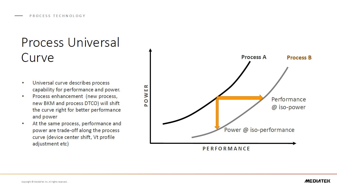
TheProcess Universal Curvedescribes the fundamental trade-off betweenperformanceandpowerin semiconductor manufacturing. At any given process node, there is a clear boundary that defines the achievable combinations of performance and power. When performance is increased, it typically comes at the cost of higher power consumption; conversely, reducing power requires a sacrifice in performance. This curve represents the envelope of all feasible design points under the constraints of that specific process technology.
As process technologies advance—whether through the adoption of new materials, improved best-known manufacturing practices (BKM), or Design-Technology Co-Optimization (DTCO)—the entire curve canshift downward and to the right. This means that, under the same power budget, higher performance can be achieved, or conversely, the same performance can be reached with reduced power consumption. In the illustrative case ofProcess A versus Process B, Process B demonstrates superior characteristics:
Atiso-power, Process B delivershigher performance.
Atiso-performance, Process B achieveslower power consumption.
Even within the same process node, designers can further optimize trade-offs by fine-tuningthreshold voltage (Vt),device centering, and other transistor-level parameters. This allows chip architects to tailor designs to different application needs—maximizing performance for high-end servers, or minimizing power consumption for mobile devices.
In essence, theProcess Universal Curveserves as a crucial metric for evaluating process improvements, especially as demands from AI, high-performance computing (HPC), and ultra-low-power edge devices become increasingly diverse. The ability to shift this curve effectively is now a core indicator of a process technology’s competitiveness.
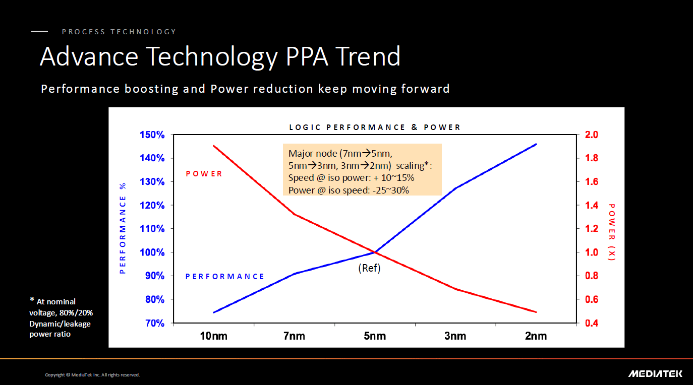
The Evolutionary Trend of Advanced Process Nodes in Performance and Power — The “PP” in PPA
In advanced logic process technology, the evolution from 10nm to 7nm, 5nm, 3nm, and now toward 2nm nodes has brought consistentperformance improvementsandpower reductions—the two key pillars of thePPA (Performance, Power, Area)framework.
According to statistical data shown in the referenced chart, undernominal voltage operating conditionsand assuming a typical power composition of80% dynamic powerand20% leakage power, each generational node shrink (e.g., from 7nm → 5nm, 5nm → 3nm, 3nm → 2nm) generally delivers:
Approximately10–15% performance improvement(at iso-power), and
Around25–30% power reduction(at iso-performance).
In the chart, theblue curverepresents increasing performance with each node shrink, while thered curveshows a downward trend in power consumption. Around the5nm node, these curves intersect at a keyreference point, marking a pivotal inflection in technology development. As the industry moves further into the 3nm and 2nm generations, the divergence between performance gains and power savings becomes even more pronounced.
This is largely due to not only increasedlogic densityfrom finer geometries but also enhancements intransistor architecture(e.g., the transition from FinFET toGate-All-Around (GAA)structures) andmaterials innovation. Together, these advances enable substantial improvements in overall system efficiency.
In summary, this trend reinforces the continued value of advanced process nodes for applications such asAI,HPC,mobile devices, andlow-power edge computing. It is also why companies likeMediaTekandNVIDIAare investing in 3nm and 2nm nodes as foundational technologies for futureAI ASICs, SoCs, intelligent edge platforms, andautomotive systems.

Area Scaling Trends in Advanced Process Nodes: The Bottleneck of SRAM Miniaturization
One of the fundamental promises of advanced process nodes has long beenchip area reduction—enabling higher logic density and improved cost efficiency. Traditionally, process scaling has resulted in significant shrinkage of bothlogic standard cellsandSRAM bitcells, leading to substantial gains in overall chip integration. However, as the industry advances beyond the5nm node, the pace of area scaling is beginning to slow, especially for SRAM, which is now approaching its physical scaling limits.
According to industry data:
The transition from7nm to 5nmdelivered roughly30% chip area reduction.
From5nm to 4nm, this benefit dropped to about20%.
Moving from3nm to 2nm, area reduction is estimated to be only~10%.
This trend reflects a growing disparity between the scaling behavior ofstandard logic cellsandSRAM bitcells. While standard cells continue to scale at a steady pace,SRAM area scaling is plateauing, becoming the primary bottleneck in achieving meaningful chip-level area reductions.
Given thatSRAM accounts for approximately 30% of total chip areain modern SoC designs, its stagnation has a significant impact on the benefits of process scaling. As a result, industry attention is increasingly shifting toward new memory architectures such asCompute-in-Memory (CIM)and3D-stacked memorysolutions, which aim to overcome density bottlenecks by rethinking the role and integration of memory.
In summary, this trend underscores a major shift:process node evolution is no longer just about shrinking physical gate lengths, but about entering a new phase driven byarchitectural innovation,materials breakthroughs, andDesign-Technology Co-Optimization (DTCO).
For companies likeMediaTekandNVIDIA, which are heavily invested inAI ASICsandhigh-density SoCs, these constraints will be a critical factor in future design and manufacturing decisions. Sustaining Moore’s Law and performance-per-area improvements will increasingly rely on innovations beyond traditional scaling.

Transistor Cost Reduction in Advanced Nodes: Slowing Down and Facing Reversal at 2nm and Beyond
In advanced semiconductor nodes, the long-standing trend oftransistor cost reductionis decelerating—and may even reverse as the industry enters the2nm era and beyond. Traditionally, Moore’s Law implied thattransistor density would double every two years, resulting inlower cost per transistor. However, the transition fromFinFET (Fin Field-Effect Transistors)toGAA (Gate-All-Around)architectures has introduced significantly more complex and expensive cost structures, causing a widening gap between industry expectations and real-world outcomes.
From the16nm/14nm to 10nm nodes, each generation achieved approximately30% cost reduction per transistor, which aligned with historical projections. However, the move from7nm to 5nmyielded only around a20% cost reduction. More critically, the shift from3nm to 2nm—and smaller nodes—shows signs of cost stagnation or even increase, a trend described as “flatish or worse,” wherethe cost per transistor may in fact rise.
This shift highlights the fact thatarea savings from process scaling no longer translate directly into cost advantages. Several key factors contribute to this:
High capital costsassociated withEUV (Extreme Ultraviolet Lithography)tools;
Increasedprocess complexity and step count;
Yield challengeswith new materials and architectures;
Escalatingdesign, verification, and IP reuse costsdue to greater integration complexity.
For chip design companies and system platform providers, this meansprocess node selection can no longer rely on the assumption that “more advanced is always better.”Instead, carefultrade-off analysisis needed—balancing cost, power efficiency, performance, and market fit.
Companies such asMediaTekandNVIDIA, which are deeply invested in ASIC development and advanced packaging technologies, must increasingly adopt strategies such as:
DTCO (Design-Technology Co-Optimization)andSTCO (System-Technology Co-Optimization);
Leveraging packaging innovations likechiplets,3D IC, andCo-Packaged Optics (CPO);
In summary, the future of scaling is not solely defined by physical gate length reduction—but by the ability tointegrate architecture, process, and packaging strategiesto deliver sustainable performance and economic value.
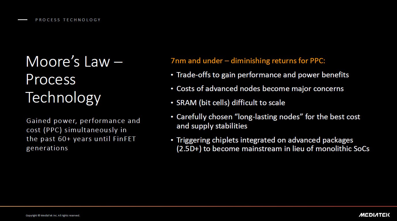
The Bottlenecks and Transformation of Moore’s Law in the Sub-7nm Era
For over six decades, the continuous evolution of process technology has simultaneously delivered improvements inpower,performance, andcost—the “PPC” trifecta that has underpinned the rapid progress of the semiconductor industry. However, this golden era began to stall with the advent ofFinFETtechnologies, and the slowdown has become increasingly evident in thesub-7nm nodes. Today, thediminishing returnsof PPC scaling are a central challenge to Moore’s Law.
First, the performance and power benefits of advanced nodes are no longer a “free lunch”; they now requiresignificant design and process trade-offsto realize. Second,manufacturing costs have risen sharply, making cost-efficiency a critical factor in deciding whether to adopt a new node. Third,SRAM bit cell scaling has plateaued, limiting the ability to reduce overall chip area as expected. As SRAM occupies a substantial portion of SoC area and power, it has become a key bottleneck in next-generation designs.
In response, the industry has begun to embraceselective node extensionstrategies—prolonging the lifespan of “long-lasting nodes”that offer optimal cost structure and supply chain stability. This shift is also fueling the rise ofchiplet architecturesandadvanced packagingtechnologies. In particular,2.5D integrationmethods—such asCoWoS, InFO, and EMIB—are replacing the traditional approach of monolithic SoC design, becoming the mainstream architecture for system-level integration.
Overall, these changes underscore a critical transformation in the post-Moore’s Law era:innovation in chip design and system architectureis emerging as the primary engine of semiconductor progress. The transition from traditional node scaling toSystem Technology Co-Optimization (STCO)marks a pivotal inflection point for the industry—wheresystem-level designbecomes the new frontier of technological advancement.
MediaTek Joins Forces with Google: Strategic Entry into TPU Design and Its Future Implications
Amid the increasingly fierce competition in AI data center chip development, Google is accelerating its diversification of in-house AI chips and decentralization of its hardware supply chain. One of the most notable moves is its collaboration with Taiwanese chip design leaderMediaTek: the two companies will co-develop thenext-generation TPU (Tensor Processing Unit)chip, slated for mass production in2026, marking a significant step in the evolution of AI infrastructure.
From Broadcom to MediaTek: A Strategic Shift in Google’s TPU Partnerships
For years, Google has primarily partnered with Broadcom for the development of its TPU series, particularly for the fifth and sixth generations (TPU v5 / v6 Trillium), with Broadcom providing extensive custom ASIC design support. However, as the cost of large AI models continues to rise and cloud infrastructure faces mounting pressure, Google is now expanding its supplier base in search of greater cost-efficiency and design flexibility.
The collaboration with MediaTek focuses on theI/O modules and peripheral logicof theseventh-generation TPU (TPU v7), while Google continues to lead the development of the core processor. The chips will be manufactured byTSMCusing advanced process nodes.
This partnership highlights two major industry trends:
Deeper Functional Disaggregation in AI Chip Design: Hyperscalers are moving away from relying on a single vendor, instead partitioning core and peripheral functions among different partners to enhance flexibility and cost control.
Diversification of ASIC Design Platforms: While MediaTek is best known for mobile SoCs, its expertise in high-speed SerDes, advanced packaging, and power efficiency optimization is becoming a gateway to data center-grade applications.
TPU v7: Expected Specs and Production Timeline
While full specifications for TPU v7 remain undisclosed, current reports and supply chain insights suggest the following:
Continued use ofTSMC’s 3nm node, with architectural optimizations for both AI training and inference.
Expansion of TPU clustersfrom 256 chips to up to9,216-chip arrays, enabling large-scale inference for AI foundation models.
Higher bandwidth I/O channels—designed by MediaTek—to support high-speed switching and data transfer.
According to external research reports, the Google–MediaTek project is facing some delays, mainly due to internal setbacks in Google’s processor design schedule. Mass production is now expected to slip from early 2026 to the second half of the year, which may impact MediaTek’s revenue recognition timeline.
Why MediaTek?
From Google’s perspective, MediaTek offers several strategic advantages:
Deep familiarity with TSMC nodes: MediaTek has a long-standing, close relationship with TSMC, ensuring seamless integration with advanced processes and packaging platforms.
Strong cost-efficiency and area optimization: Known for delivering high-performance yet cost-effective SoCs, MediaTek excels in optimizing power and die size.
Fast time-to-market: MediaTek brings exceptional execution capabilities in SoC sampling and mass production, from mobile to edge applications.
Moreover, MediaTek’s experience inadvanced packaging and high-speed interfaces(e.g., die-to-die, UCIe, HBM with 2.5D integration) makes it a compelling partner for developing TPU I/O subsystems.
What This Means for MediaTek: From Mobile SoCs to AI Data Centers
This marks MediaTek’sfirst major involvement in the design and production flow of data center-class AI chips, representing not only a branding milestone but also a pathway to enter the AI infrastructure market.
Initial analyst estimates projected over$2.4 billion in ASIC-related revenuefor MediaTek between 2025 and 2026. Due to project delays, this has been revised down to roughly $1.6 billion. However, if the platform is successfully commercialized, it could provide MediaTek with the credibility and foundation to attract future cloud-scale ASIC contracts.
A New Experiment in AI Chip Disaggregation
The Google–MediaTek partnership is more than just a commercial engagement—it represents anew experiment in AI chip disaggregation and supply chain decentralization. As major AI players seek to diversify away from traditional suppliers, the ability to find partners that combine integration capabilities, cost efficiency, and process compatibility will be crucial to reducing total system costs and scaling effectively.
For MediaTek, this is ahigh-stakes, high-leverage bet—one that, if successful, could dramatically expand its footprint in the global ASIC market and pave the way for a transition from device-edge champion to a serious data center player.

2.5D and 3.5D Advanced Packaging Architectures: Comparing TSMC’s CoWoS and Intel’s EMIB
In the field of advanced semiconductor packaging,2.5D and 3.5D integration architectureshave emerged as crucial solutions for heterogeneous integration, offering high bandwidth, scalability, and system-level performance. Two of the most prominent technologies in this domain areTSMC’s CoWoS (Chip-on-Wafer-on-Substrate)andIntel’s EMIB (Embedded Multi-die Interconnect Bridge).
TSMC CoWoS Series
CoWoS is aTSMC-developed 2.5D packaging platformthat mounts multiple dies—such as ASICs and HBM—on asilicon interposer, which is then placed onto an organic substrate. Based on the type of interposer used, CoWoS is subdivided into three variants:
CoWoS-S: Utilizes afull silicon interposer, offering high wiring density and low latency for high-performance applications.
CoWoS-L: Employs alocal silicon bridgecombined withRDL (Redistribution Layer)to reduce silicon area and cost while maintaining bandwidth.
CoWoS-R: Eliminates the silicon interposer, using onlyRDL layerson an organic interposer for lower-cost, more flexible designs.
Intel EMIB
In contrast, Intel’sEMIBadopts abridge-based interconnectwithout requiring a full silicon interposer. Instead,small silicon bridges are embedded directly into the organic substrate, enabling high-speed die-to-die communication. This architecture allows for scalable, large-area die placement by adjusting the number and layout of bridges, while alsosimplifying the overall manufacturing process.
The Rise of 3.5D Integration: SoIC-X
As packaging evolves beyond 2.5D,3.5D integrationtechnologies such asTSMC’s SoIC-X (System-on-Integrated-Chips eXtended)are gaining traction. SoIC-X enablesvertical die stackingon top of a 2.5D platform—such as CoWoS-S or CoWoS-L—by adding a second layer of active dies. This hybrid architecture significantly improvesintegration density, performance, and bandwidth, making it ideal forAI computing, data center infrastructure, and HPC applicationsthat demand high logic and memory co-location.
The transition from 2.5D to 3.5D represents a shift fromhorizontal integrationtohybrid vertical stacking. By leveraging various interposer and bridge technologies—such asRDL,TSV, andsilicon bridges—chip designers can now optimize for performance, cost, and thermal management requirements. These packaging platforms are becoming essential for overcoming the limitations of traditional scaling.
MediaTek, for example, is actively adopting and integrating both CoWoS and EMIB technologies to strengthen its capabilities inhigh-performance heterogeneous integrationandcustom ASIC design—positioning itself competitively in next-generation compute platforms.

Future Scalability of CoWoS and EMIB in Heterogeneous Integration Packaging
CoWoS (Chip-on-Wafer-on-Substrate)andEMIB (Embedded Multi-die Interconnect Bridge)represent two distinct approaches to advanced heterogeneous integration, each with unique strengths and scalability pathways for future compute platforms.
CoWoS: Bandwidth-Driven Vertical Expansion with Integration Limits
CoWoS leverages alarge-area silicon interposer, enablinghigh-bandwidth, low-latency chip-to-chip interconnects, making it ideal forAI, HPC, and server applications. However, as the interposer size increases,physical and economic constraintsemerge—includingprocess-induced stress,reticle cost,yield management, andreticle-limited die size. These factors are placing pressure on CoWoS to evolve beyond horizontal integration.
The natural extension of CoWoS is toward3.5D architecturessuch asTSMC’s SoIC, wherevertical stackingof compute and memory dies increases density without expanding substrate footprint. In the future, CoWoS platforms are also expected to incorporate advanced features such asIVR (Integrated Voltage Regulators)andSiPh/CPO (Silicon Photonics / Co-Packaged Optics)modules to form comprehensive compute subsystems. However,system-level scalingin CoWoS may be capped at around10× integration densitydue to interposer size and thermal constraints.
EMIB: Flexible Interconnects with Room for Horizontal Scaling
In contrast, EMIB employsembedded silicon bridgesdirectly into theorganic substrate, enablinglocalized high-density interconnectswithout the need for a full silicon interposer. This approach offersgreater design flexibility, betteryield scalability, and lower overall cost for complex multi-die systems.
The primary challenges for EMIB lie invertical mechanical stress,bridge placement pressure, andpackage warpage. Yet with continued advances insubstrate engineeringandmaterials technology, EMIB—particularly its extended version,Co-EMIB—shows strong potential forscaling beyond 10× die integration, surpassing its original integration envelope.
In summary,CoWoSis well-suited for applications that demandmaximum bandwidth and vertical integration, and will likely continue along the3.5D stacking path.EMIB, on the other hand, excels inmodular flexibility and manufacturability, and holdsgreater long-term potentialfor large-scale system expansion.
Together, these technologies will continue to serve ascomplementary pillarsin the roadmap forheterogeneous system integration, enabling chip architects to choose the optimal platform based onperformance, yield, form factor, and cost targets.
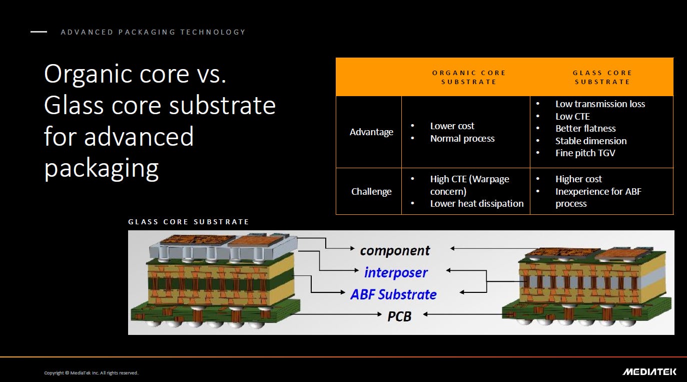
A Critical Inflection Point in Core Substrate Materials for Advanced Packaging
In the domain ofadvanced semiconductor packaging, the choice ofcore substrate materialis reaching a pivotal juncture—particularly as high-frequency, high-speed applications such asAI chips,HPC modules, andhigh-speed I/O systemscontinue to grow rapidly.
Traditionally, theorganic core substratehas remained the mainstream choice due to itscost-effectivenessandmature manufacturing ecosystem. However, its inherent limitations are increasingly evident under next-generation workloads. These include:
Higher Coefficient of Thermal Expansion (CTE), which leads to warpage risks;
Inferior thermal conductivity, which impacts system reliability and performance;
As a result, organic substrates are struggling to meet the evolving demands of high-performance, high-reliability systems.
In contrast, theglass core substrateis gaining traction as a promising next-generation solution due to its:
Extremely low transmission loss;
Excellent dimensional stability and flatness;
Low CTE, which helps mitigate warpage;
Compatibility with ultra-fine-pitch TGVs (Through-Glass Vias).
These attributes make glass core substrates especially suitable formulti-die integration,3D stacking, andopto-electronic co-packaged modules (e.g., CPO). In such applications, advantages insignal integrity,warpage control, andfine via layoutbecome particularly critical.
However, the adoption of glass substrates facestwo major challenges:
Higher material and process costs, which pressure volume production economics;
Limited industry experience and process maturity, especially in relation toABF (Ajinomoto Build-up Film)compatibility and scaling.
Thus, whileglass core substrateshold strong potential to become a mainstream solution,widespread adoption will require time and coordinated ecosystem support. The future trajectory will depend on how well the industry can balancesystem-level performance requirementswithmanufacturing cost and scalability, and how quicklyproduction technologiesfor glass substrates can mature.
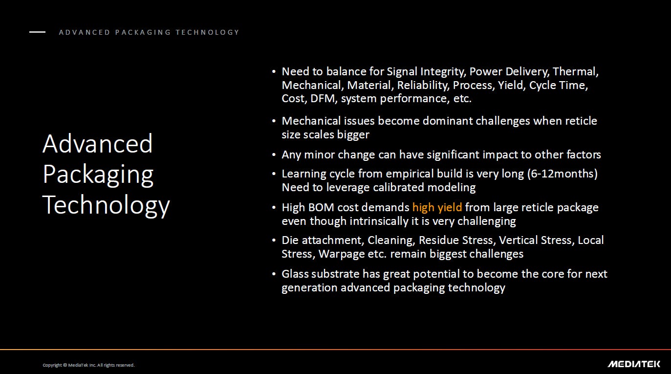
Scaling Advanced Packaging: Multidimensional Challenges and the Rise of Glass Substrates
Asadvanced packagingtechnologies evolve towardlarger-scale and higher-performance integration, they are encounteringunprecedented multidimensional challenges. Beyond the traditional concerns ofsignal integrity (SI),power delivery (PD),thermal management, andmaterials selection, engineers must now also navigate complex trade-offs involvingyield,reliability,manufacturing cycle time,cost, anddesign for manufacturability (DFM).
Once die sizes approach thereticle limit,mechanical issuesbecome dominant constraints—particularlyvertical stress,localized warpage, andresidual mechanical strain. These effects can directly impact both yield and long-term reliability of packaged systems.
The packaging development cycle is typicallylong and iterative. From initial prototype to process optimization, it can take6 to 12 monthsof repetitive experimentation. To reduce this timeline, highly accuratemodeling and simulation toolsare essential. Meanwhile, thehigh bill of materials (BOM) costof advanced packages demands extremely high yield to ensure commercial viability—yet achieving stable, high yield remains difficult, especially inlarge-area packages.
Even minor process variations—such asbonding alignment,cleaning protocols, orresidue control—can lead tosignificant fluctuations in reliability and yield. Within this context,glass substratesare increasingly recognized as acore enabling materialfor next-generation advanced packaging. Thanks to theirdimensional stability,low coefficient of thermal expansion (CTE), and superiorwarpage control, glass substrates offer strong growth potential in areas such aslarge-area integration,heterogeneous packaging, andhigh-frequency applications.
SemiVision Technical Insight Series: Unpacking MediaTek’s Innovation Across Seven Strategic Dimensions
1.MediaTek’s Strategy and Challenges in Advanced Packaging: CoWoS, EMIB, CPO, and Glass Substrates
In recent years,MediaTekhas actively invested inadvanced packaging technologiesto enhance the competitiveness of its high-performance chips. In the high-performance computing (HPC) domain, MediaTek has adoptedTSMC’s 2.5D CoWoS® (Chip-on-Wafer-on-Substrate)technology, integrating high-speed compute dies with high-bandwidth memory (e.g., HBM) to meet the growing demand for bandwidth and memory capacity in AI training applications.
At the same time, MediaTek is also exploringIntel’s EMIB (Embedded Multi-die Interconnect Bridge)and related3D stackingapproaches to evaluate their potential for heterogeneous integration. However, building proprietary advanced packaging capabilities presents significant challenges—includingyield control,thermal management, andhigh manufacturing costs. To overcome these limitations, MediaTek has opted to collaborate withecosystem partnersto close capability gaps in packaging.
A notable example is MediaTek’s effort inCo-Packaged Optics (CPO). The company has partnered with Canadian optical communication firmRanovusto develop acustom ASIC design platform. This platform integrates MediaTek’s proprietary112G long-reach SerDeswithRanovus’ Odin® optical enginewithin the same package, supporting both8×800 Gbps electrical linksand8×800 Gbps optical links. This hybrid electro-optical packaging significantly reduces PCB footprint, lowers overall system cost, and cuts system power consumption by up to50%. Ranovus’ optical engine supports bothintegrated and external laser modules, allowing flexibility for different deployment scenarios. Through this partnership, MediaTek has bridged its knowledge gap insilicon photonics and optical packaging, enabling entry into the next wave ofoptical I/O integration for AI and HPC chips.
Looking further ahead, MediaTek is also exploringglass core substratesas the next-generation interposer technology. Glass interposers offer advantages such aslarger panel sizes,low CTE (coefficient of thermal expansion)close to that of PCBs, andbetter dimensional stability. These features make glass a promising alternative to silicon interposers, which are constrained by die size limits and high fabrication costs. MediaTek believes that asAI chip sizes continue to increase, glass substrates will be essential forreducing packaging costsandenhancing signal integrity. However, challenges remain, includingprocess reliabilityandadvanced metallization techniques, and broader adoption will depend on the maturity of the supply chain.
In summary,MediaTek’s strategyinvolves leveraging existing platforms such asInFO and CoWoS, while proactivelypartnering with specialized ecosystem players. The company is building momentum in advanced packaging, but must continue addressing persistent challenges inyield, materials, and production scalabilityto support future high-end chip development.
2.Collaboration Between MediaTek and NVIDIA on AI ASIC and NVLink Technologies
MediaTek’s strategic partnership with NVIDIAhas enabled the company to enter the AI accelerator market. A major milestone in their collaboration was the joint launch of theGB10 superchip in 2025, a system-on-chip (SoC) built on NVIDIA’sGrace-Blackwell architecture. The GB10 integrates a20-core Arm-based Grace CPUand a next-generationBlackwell GPU, connected via the high-speedNVLink-C2Cchip-to-chip interface.
MediaTek played a key role inoptimizing the design of GB10, contributing its expertise inhigh-efficiency Arm SoC designto achieve an optimal balance ofpower, performance, and connectivity. The GB10 delivers1 PetaFLOPS of AI compute performance (FP4 precision)while operating within a power envelope that can be supplied by a standard desktop outlet—making itthe world’s smallest AI personal supercomputer core. The chip serves as the core of NVIDIA’sProject DIGITS (DGX Spark)personal AI supercomputer, representing a broader industry trend of AI computemoving from the data center to the desktop.
High-Speed Interface and Custom ASIC Integration
Throughout the collaboration, MediaTek and NVIDIA have focused onhigh-speed interconnects and custom ASIC design. MediaTek integrated its ownhigh-speed SerDes and bus technologieswith NVIDIA’sNVLink architectureto enablelow-latency, high-bandwidth communicationbetween CPU and GPU dies. NVLink-C2C not only connects CPU and GPU cores within the GB10 but is also expected to supportmulti-die expansionacross modular packages.
AtComputex 2025, NVIDIA CEOJensen Huangappeared alongside MediaTek executives to formally launch theNVLink Fusion ecosystem, with MediaTek named as one of the first partners. NVLink Fusion is anopen high-speed interface standarddesigned to allow multiple vendors to co-developsemi-custom AI infrastructure. Other initial partners includeMarvell,AIChip,Astera Labs, andSynopsys. Through NVLink Fusion, hyperscale systems can interconnect ASICs with NVIDIA cabinet-scale platforms via800 Gbps-class links, enabling efficientmulti-chip collaboration.
Huang emphasized that NVLink Fusion opens up NVIDIA’s AI platform to ecosystem partners, enabling them tochain multiple AI chips togetherwith unprecedenteddata movement efficiencyacross dies.
Future Outlook
Looking forward, the MediaTek-NVIDIA partnership is likely toexpand beyond CPU/GPU integrationinto a broaderAI acceleration roadmap. MediaTek’s strengths inSerDes and high-speed interconnecttechnology, combined with NVIDIA’s leadership inGPU compute and software ecosystems, create a strong foundation for future collaboration. Potential developments may include:
Co-developing custom AI chipsfor hyperscale data centers and cloud customers,
Deepening automotive collaborationsby combining each company’s strengths,
Enabling third-party AI chips to integrate with the NVLink ecosystem.
MediaTek Vice ChairmanRick Tsaicommented that the partnership, which began with automotive SoCs, has now expanded intocloud-scale AI infrastructure. MediaTek will leverage itsworld-class ASIC design servicesandinterconnect expertiseto co-architect thenext generation of AI platformswith NVIDIA—delivering scalable, efficient, and flexible solutions for modern cloud AI demands.
This marksMediaTek’s evolution from a mobile device chipmakerinto a key partner forNVIDIA in the AI era, contributing to the future of open, heterogeneous AI compute systems.
3.Differentiating Products Through Advanced Packaging: MediaTek’s Path into Cloud AI and HPC
To enter thecloud AI and high-performance computing (HPC)markets,MediaTekmust extend beyond its traditional strengths and developdifferentiated product capabilities.Advanced packaginghas become a key strategic enabler in this transformation. By leveraging2.5D/3D integration, MediaTek can combine heterogeneous chiplets into a single module—significantly improvingsystem performanceandfunctional density.
This approach enableschiplet-based architecture, allowing MediaTek to fabricate distinct functional modules (e.g., compute cores, I/O interfaces, memory) onoptimized process nodes, and then interconnect them through high-density packaging. For instance, indata center AI accelerator cards, MediaTek can integrate high-performance compute dies with multipleHBM memory stacksusingTSMC’s CoWoS silicon interposer, deliveringmassive bandwidth and memory capacitythat traditional SoCs struggle to achieve. This level of integration positions MediaTek’s solutions to handle large-scale AI model training and data throughput, effectively providing agateway into HPC workloads.
Beyond hardware performance, advanced packaging enablesnew modes of customer differentiationthroughcustom ASIC design services. In 2024, MediaTek announced aturnkey ASIC platform, offering end-to-end solutions fromdesign to production. The platform includes:
High-speed die-to-die interconnects such as MediaTek’s proprietaryMLinkand open standardUCIe,
Support for various advanced packaging methods, includingInFO,CoWoS, andHybrid CoWoS,
Integration of high-speed I/Os likePCIe,Ethernet, andoptical modules.
This offering goes beyond chip design—MediaTek positions itself as atotal solution provider, managing advanced packaging and system integration to delivercustom chipstailored to the needs of cloud service providers and AI hardware vendors. Throughpackaging-level customization(e.g., thermal optimizations, modular interface designs), MediaTek can createproduct-level differentiationto stand out in a competitive market.
It’s worth noting that MediaTek has traditionally focused onmobile SoCs, making it a latecomer to the HPC space. However, the AI era has fueled a surge incustom ASIC demandfrom cloud operators seeking domain-specific accelerators. MediaTek seized this opportunity, combining itsenergy-efficient SoC design expertisewith advanced packaging to deliverhigh-performance, power-efficient AI accelerators.
For example, MediaTek has already enteredvolume productionof HPC-class chips usingTSMC’s advanced nodes and CoWoS packaging, reportedly shipping to cloud customers as early as 2023. Additionally, MediaTek’s partnership withRanovusforCo-Packaged Optics (CPO)gives its solutions greater scalability—enabling the addition of more compute nodes with lower power interconnects. These differentiators have helped MediaTek secure a position in the highly competitive cloud AI and HPC markets.
Looking ahead, MediaTek plans to deepen its investment in packaging innovation to maintain its competitive edge. Potential directions include:
3D SoIC chip stackingto add local cache memory for improved performance,
Adoption oflarge-format glass interposersto reduce packaging cost while improving signal integrity.
Together, these strategies will reinforce MediaTek’s role as anext-generation infrastructure chip partner—offering differentiated, scalable, and energy-efficient platforms for the AI and HPC era.
- Automotive Market Strategy: 3nm DX1 Platform, 5G Cockpit Integration, and Packaging Challenges
MediaTekhas made significant inroads into the automotive semiconductor market in recent years, launching itsDimensity Autoplatform series to meet the evolving demands of next-generation intelligent vehicles. The flagship cockpit SoC,CT‑X1 (code-named DX1), is built usingTSMC’s advanced 3nm process, making it one of the world’s first automotive-grade chips at this node. CT‑X1 is based on theArm v9.2-A CPU architecture, integrating a powerfulAI processing unitanddeep learning accelerator, and also incorporatesNVIDIA’s Blackwell GPU IP, forming adual-AI engine architecture.
This chip delivers cutting-edge compute performance—capable of runninglarge language models (LLMs) with up to 13 billion parametersand generative AI applications likeStable Diffusiondirectly within the vehicle. With robustedge AI computing, CT‑X1 supports advanced in-vehicle features such as3D graphical voice assistants,multi-screen infotainment, anddriver monitoring, all while maintaining low latency and high responsiveness.
Cockpit-Connectivity Convergence and 5G Integration
MediaTek’s automotive strategy emphasizescockpit-connectivity convergenceandcomprehensive in-vehicle integration. On the connectivity side, MediaTek launched its flagshipvehicle modem platform, MT2739, which includes a5G-Advanced modemsupporting3GPP Release 17/18andNB-NTN satellite communication. MT2739 isAEC-Q100 Grade 2 qualifiedand offers features likedual-SIM dual-active supportandAI-driven network optimization, ensuring high-performance, reliable in-vehicle connectivity.
Looking forward, MediaTek plans tofurther integrate 5G modem capabilities into its cockpit SoCs, moving toward a“cockpit + communication” single-chip solution. This integration would enable automakers to deployunified automotive electronic systems, supporting features like real-time cloud services, OTA updates, andcloud-cooperative AI model execution.
Packaging Challenges in Automotive Applications
Advanced packaging technologiesare playing an increasingly vital role in automotive chips—but they also present unique challenges. Automotive electronics must operate reliably underextreme environmental conditions(−40°C to 125°C) andprolonged mechanical stress, requiringrobust packaging structures. MediaTek addresses this by selecting materials and designs that withstandthermal cyclingandmechanical strain, such as:
Thicker solder bumps,
Flexible organic substrates, and
Collaboration with OSAT partners likeASE and SPILforreliability testingin compliance withAEC-Q standards.
Thermal management is another concern. High-performance SoCs in vehicles can consume significant power, requiring efficient heat dissipation. MediaTek may employflip-chip BGA with heat spreaders, orintegrated thermal conduction structureswithin the package to extract heat from the die surface.
Moreover, 3nm chips are physically small with extremely high I/O density, posing challenges inassembly and yield control. MediaTek leverages its mobile SoC experience—such asPoP (Package-on-Package) memory stackingandInFO advanced packaging—to refine yield and packaging reliability for automotive-grade SoCs.
Longevity and Process Diversity Strategy
The automotive market demandslong-term supply stabilityandproduct longevityfar exceeding consumer-grade products. MediaTek’s automotive product roadmap reflects this, balancing leading-edge innovation withsupply risk mitigation. In addition to the flagship3nm CT‑X1, MediaTek offers the4nm CT‑Y seriesfor premium vehicles and is exploring6nm/7nm nodesfor mid-tier automotive SoCs—ensuring sustainable product supply over multiple years.
Thistiered process strategy, combined withflexible packaging solutions, allows MediaTek to serve diverse vehicle segments while minimizing manufacturing risks. Coupled with the incorporation ofNVIDIA’s advanced GPU and AI IP, MediaTek is rapidly gaining competitiveness in the automotive semiconductor space.
- Edge AI Product Line: GB10 and Multi-Agent (MCP/A2A) Architecture Enabled by Advanced Packaging
With tightly integratedCPU and GPU cores, along with128GB of unified memory, GB10 can execute large-scale models withtens to hundreds of billions of parametersdirectly on-device. This allows AI developers totrain and test prototypes locallyand seamlessly deploy them to the cloud, fostering acloud-to-edge collaborative model. To support such advanced local performance, MediaTek employs multiplepackaging and interconnect innovations:
NVLink-C2Cconnects CPU and GPU dies directly at high bandwidth and low latency.
Multi-die packagingis used to ensure rapid data movement within the chip.
2.5D integrationof HBM memory close to compute dies significantly increases memory bandwidth—crucial for processing large context windows in modern AI models.
Multi-Agent AI Architecture: Hardware-Software Co-Design
Concurrently, the AI industry is moving towardmulti-agent collaboration models, such as Google’sA2A (Agent-to-Agent)protocol and Anthropic’sMCP (Model Context Protocol). These frameworks allow multiple AI agents tocommunicate and collaborate, or a single AI model to invoke external tools and resources.
Edge AI devices of the future may need torun multiple specialized agents simultaneously—voice assistants, image recognition, decision engines, etc.—working together to complete complex tasks. MediaTek’s hardware is well-aligned with this trend: its AI SoCs integratevarious processing units (NPU, DSP, GPU)in a single package usinghigh-speed die-to-die interconnects(e.g.,UCIeor proprietary interfaces), creating anon-chip AI communication backbone. This allows agents tocollaborate locallywithout frequent trips to the cloud.
For example, an Edge AI SoC may contain multiple compute engines packaged as asystem-in-package (SiP)using2.5D/3D integration, minimizing signal latency and maximizing bandwidth between processing units. In such a design, MediaTek ensures that agents likevoice assistants, camera AI, and smart home controllersoperate in parallel and coordinate efficiently—mirroring theA2A vision of seamless, task-specific collaboration.
Packaging as the Enabler of Multi-Agent AI
Advanced packaging plays a critical role in enabling this architecture:
2.5D/3D integrationcombines heterogeneous dies into a compact SiP, reducing inter-core latency.
PoP or HBM stackingprovideshigh-speed memory cachesto support shared context data for multiple agents.
For instance, in a smart home AI hub:
Thevoice assistant agentmay require sustained access to memory forconversational context, aligning withMCP’s model state management.
Thevision agentmust performreal-time video inferencewith high compute demand.
MediaTek’s packaging solution places DRAM physically close to AI compute cores and establisheslow-latency internal buseswithin the package. This ensures that both agents can access shared data swiftly and communicate without bottlenecks.
Toward the Edge AI Factory Model
Suchhardware-software synergysupports the vision of an“AI factory” at the edge—an edge device runningmultiple interactive AI agentslocally, capable of fulfilling complex, real-time tasks in smart homes or cities. MediaTek is building toward this future by combining itsadvanced packaging expertise,efficient SoC design, andsupport for emerging AI protocols, offering a blueprint fornext-generation distributed AI computing.
- Packaging Challenges and Solutions in the FinFET/GAA Era: PPA Optimization, SRAM Bottlenecks, and Cost Control
As chip manufacturing moves toward the end of the FinFET era and into the Gate-All-Around (GAA) generation (e.g., 3nm and 2nm nodes), the traditional benefits of Moore’s Law scaling have begun to diminish. MediaTek now faces new challenges in optimizing performance, power, and area (PPA). One of the most pressing issues is the SRAM scaling bottleneck: SRAM cell area is shrinking far less than logic circuits, causing the cache area ratio on chips to increase rather than decrease, alongside growing concerns over leakage and reliability.
To address this, MediaTek has adopted a multi-pronged strategy. On the design level, the company seeks to minimize reliance on large on-die SRAM caches by employing architectural optimizations and advanced techniques—such as compression and intelligent scheduling—to boost cache hit rates, or by integrating more efficient memory IPs. More proactively, MediaTek leverages heterogeneous packaging to offset the limitations of advanced process nodes. For instance, part of the memory can be moved off the main die and integrated as discrete cache or memory dies within the package. High-speed SRAM or even embedded DRAM (eDRAM) dies can be placed alongside the logic die via 2.5D silicon interposer technology, effectively acting as “L4 cache” that offers several times the bandwidth of off-package DRAM. Looking ahead, with technologies like TSMC’s SoIC (System on Integrated Chips), vertical stacking of SRAM directly atop processors may become feasible—creating a “chip-on-chip” cache extension that significantly reduces data transfer latency. These are among the approaches under consideration at MediaTek to overcome the stagnating performance of SRAM in advanced nodes.
Additionally, MediaTek uses die-size reduction and multi-die architectures to enhance yield and manage power. Rather than building a single, large monolithic die, the system is split into smaller chiplets, each fabricated using the most suitable process node and interconnected via advanced packaging. This chiplet approach reduces yield risks inherent to large die sizes at advanced nodes and enables the use of low-power legacy nodes for non-critical modules. MediaTek’s ASIC service offerings explicitly support MCM (multi-chip module) and SiP (System-in-Package) designs. Through 2.5D silicon bridges or organic substrate-embedded interconnect bridges (known as 3.5D packaging), MediaTek can retain analog/IO circuits on mature 22nm/28nm nodes while using 5nm or 3nm for high-performance cores—tightly integrated within the package.
This strategy of heterogeneous integration using long-lifecycle nodes is particularly valuable in automotive and IoT markets, where mature processes offer better reliability and cost efficiency. MediaTek’s approach ensures that performance-critical modules adopt cutting-edge nodes, while cost and long-term supply are controlled through mature node adoption.
Cost is an unavoidable reality in advanced packaging. Technologies like CoWoS (Chip-on-Wafer-on-Substrate) silicon interposers or 3D stacking are expensive and face capacity limitations. MediaTek addresses this through two main strategies. First, technical innovation: the company explores lower-cost “3.5D packaging” alternatives—typically involving small bridge chips embedded in organic substrates to replicate 2.5D-like interconnects at lower cost. Intel’s EMIB and TSMC’s LIPINCON are examples of such technologies. MediaTek can adopt these solutions selectively based on application requirements to reduce materials cost.
Second, economies of scale: by deploying advanced packaging across a diverse product portfolio—including HPC and automotive chips—MediaTek can negotiate better pricing and capacity support from its supply chain. In its 2025 supplier summit, MediaTek emphasized the strategic importance of advanced packaging in the AI era and called for greater supply chain collaboration, with the goal of amortizing unit costs over larger volumes. Finally, design-stage optimization also plays a key role: MediaTek engineers rely on simulation tools to assess performance accurately and simplify the package structure wherever possible—such as minimizing interposer size—without compromising functionality.
In conclusion, as MediaTek faces the FinFET/GAA-era challenges, it no longer relies solely on process scaling for performance gains. Instead, it is shifting toward a dual-path innovation model of “process + packaging.” Through heterogeneous integration, chip disaggregation, and long-lifecycle node strategies, MediaTek continues to improve PPA while avoiding some of the economic and technical pitfalls of cutting-edge processes—preparing itself for the next phase of semiconductor evolution.
- End Applications: Voice Assistants, Smart Home, and AI Tablet Strategy — Empowered by Advanced Packaging and AI ASIC Integration
In the realm of end devices, MediaTek is deeply embedding AI capabilities into voice assistants, smart home devices, and AI tablets, delivering intelligent, power-efficient, and high-performance experiences.
Voice Assistants: Compact, Low Power, and Real-Time AI Performance
MediaTek is the world’s largest supplier of voice assistant device (VAD) chips. A wide range of brands—spanning smart speakers to home appliances with embedded voice assistants—adopt MediaTek’s solutions. By integrating CPU, DSP, wireless modules, and AI accelerators (APUs) into a single chip, MediaTek’s highly integrated SoC design leverages package-on-package (PoP) technology to tightly couple memory (e.g., LPDDR, NAND) with the SoC, resulting in compact, low-power modules ideal for voice-enabled devices.
This advanced packaging ensures sufficient memory bandwidth for on-device voice recognition and response while reducing PCB routing complexity, improving signal quality and reliability. For long standby and always-on keyword detection scenarios, MediaTek optimizes ASIC designs to operate neural networks at milliwatt-level power. Additionally, low-power packaging design techniques—such as minimizing power/clock line lengths and embedding decoupling capacitors—help reduce noise and stabilize power consumption. As a result, devices powered by MediaTek chips achieve far-field voice recognition, fast response, low thermal output, and reliable long-term operation.
Smart Home: SiP Modules for Plug-and-Play Intelligence
In 2019, MediaTek launched its “Rich IoT” initiative, introducing a series of AIoT platforms to support smart home devices. These include screen-based hubs, a wide range of sensors and cameras, and autonomous home robots. MediaTek’s strategy is to offer open, universal chip platforms that integrate wireless connectivity (Wi-Fi/BT/Thread), visual processing, audio processing, and AI inference capabilities.
Through the dual advantages of highly integrated ASICs and advanced packaging, MediaTek enables plug-and-play intelligence for the smart home. Devices can connect instantly upon startup, with voice and vision AI functionalities ready out-of-the-box—meeting growing consumer expectations for convenience and simplicity.
AI Tablets and Edge Devices: High-Performance AI in Compact Form
MediaTek extends its mobile SoC expertise into AI tablets and other intelligent edge devices such as AR glasses and AI smartphones. Its Dimensity 5G platforms and newly introduced tablet-oriented AI SoCs feature dedicated AI processors capable of handling on-device tasks such as speech translation, image enhancement, and even compact GPT model inference.
To support these high-bandwidth, low-latency AI workloads, MediaTek optimizes both chip design and packaging. Advanced process nodes (such as 6nm and 4nm) reduce compute power consumption, preventing overheating during sustained AI workloads. At the same time, memory proximity enabled by advanced packaging boosts system performance. Specifically, MediaTek’s mobile SoCs commonly employ PoP packaging, stacking LPDDR memory directly above the SoC and connecting through hundreds of micro-bumps. This approach shortens data paths, lowers energy usage, and enhances performance for frequent memory access, which is critical for AI inference.
MediaTek also adopts fan-out wafer-level packaging (e.g., InFO technology) on some mobile chips to reduce package thickness and enhance power delivery and thermal performance. For power management, its SoCs integrate multiple high-efficiency buck converters and dynamically adjust AI circuit voltage and frequency in tandem with software—delivering low power during idle and high performance when needed.
Toward Ubiquitous Edge AI: Local Processing and System Optimization
Behind the scenes, chip packaging and heterogeneous integration are essential. These technologies allow complex AI SoCs to operate safely and efficiently within tight form factors and limited battery budgets. As a result, MediaTek has established a competitive edge in the end device market, offering complete platform solutions to help brand customers develop the next generation of smart products—at the intersection of IoT and AI.


PreviousNext
TopLatestDiscussions








See all