The Packaging Evolution Trilogy: Hybrid Bonding, Fluxless TCB, and 3D Stacking Ignite a Supply Chain Reshuffle
The Packaging Evolution Trilogy: Hybrid Bonding, Fluxless TCB, and 3D Stacking Ignite a Supply Chain Reshuffle
- Source: SemiVision
- Author: SEMIVISION
- Published: 2025-07-13T21:07:07+08:00
- URL: https://tspasemiconductor.substack.com/p/the-packaging-evolution-trilogy-hybrid The Packaging Evolution Trilogy: Hybrid Bonding, Fluxless TCB, and 3D Stacking Ignite a Supply Chain Reshuffle


The Packaging Evolution Trilogy: Hybrid Bonding, Fluxless TCB, and 3D Stacking Ignite a Supply Chain Reshuffle
Original Articles By SemiVision Research ( IEEE ECTC , IEEE IITC ,BESI , TSMC , UMC ,Nvidia, AMD , Intel ,TEL , Suss ,EVGroup , K&S , ASMPT ,AMAT , SHIBAURA ,SET , NYCU ,ITRI)

Jul 13, 2025
∙ Paid

The semiconductor industry is currently standing at a critical inflection point of transformation and restructuring. As AI computing demand grows exponentially, traditional Moore’s Law scaling can no longer singlehandedly sustain breakthroughs in system-level performance. In this context,advanced packaging technologiesare rapidly evolving from a “backend process” into thecore enabler of system integration and architectural innovation.
In this compute-centric technological race, whether it’s high-end AI accelerators in data centers or compact Edge AI chips deployed at the network edge, all rely on packaging solutions with higher precision, greater integration, and wider bandwidth. From TSMC’s CoWoS/SoIC platforms to the emerging heterogeneous integration strategies pursued by UMC, ASE, and SPIL, and from equipment leaders like BESI, EVG, and AMAT advancing Hybrid Bonding, to China’s aggressive investments in domestic supply chains—the direction is clear: the future lies in3D stacking + chiplet architectures + heterogeneous integration + silicon photonics.

2025年7月11日
This report series will explore the future trajectory and challenges of advanced packaging across four key dimensions: market scale, technical bottlenecks, supply chain evolution, and equipment ecosystem dynamics. We will specifically focus on the following strategic themes:
Diverse packaging demands for Edge AI: Which packaging architectures are best suited for low-power, space-constrained edge applications?
The potential of Wafer-on-Wafer (WoW) integration: Can it outperform other solutions in high-density, low-power scenarios?
Material and packaging challenges in silicon photonics: How should the industry prepare for photonic-electronic convergence?
Global competition in Hybrid Bonding supply chains: Who is driving the process transformation, and who is closing the gap?
Breakthroughs and integration among Chinese players: From homegrown equipment to production line deployment—will we see regional reshaping of the packaging supply chain?
As AI becomes a foundational infrastructure, as computation extends beyond the cloud, and as heterogeneous integration and photonic convergence become the new normal, packaging technology is no longer just an engineering challenge—it’s a strategic battleground. In the future, the question won’t just be“Who can build the chip?”, but rather“Who can integrate everything together most effectively?”
And that revolution is already underway.
Driving the Next Era of Advanced Packaging: AI, Silicon Photonics, and Co-Packaged Optics
As AI workloads rapidly scale beyond trillions of parameters, the role of advanced packaging has evolved from a passive interconnect layer into a performance-critical design platform. Today’s AI chips are no longer monolithic systems but rather chiplet-based architectures requiring ultra-high bandwidth, low-latency, and thermally efficient integration.
This has led to the convergence of several advanced technologies:
AI-driven Packaging Requirements
Modern AI chips—especially those supporting generative inference and large-scale training—demand:
2TB/s chip-to-memory bandwidth
<1ns interconnect latency
700W cooling capacity per package
To meet these demands, chipmakers are adopting 2.5D and 3D packaging with HBM stacks, ultra-fine pitch hybrid bonding, and advanced thermal materials.

Silicon Photonics and Co-Packaged Optics (CPO)

As electrical I/O (SerDes) begins to plateau at ~200G/lane, optical I/O becomes essential:
Silicon Photonicsenables monolithic integration of optical engines with CMOS logic, reducing energy per bit and improving signal integrity over long distances.
Co-Packaged Optics (CPO)moves the optical engine into the package, eliminating the power-hungry retimers and signal loss from board-level interconnects. Vendors like NVIDIA, Marvell, Ranovus, and Broadcom are deploying CPO in next-generation switches and AI systems.
However, CPO introduces new packaging challenges: sub-micron optical alignment, material stack thermal expansion mismatch, and co-integration of photonic dies with high-power logic.
Packaging as a System Platform
Major foundries and IDMs are now positioning packaging as a system-level platform:
TSMCoffers SoIC-X, CoWoS-R, and InFO-L for chiplet-based and memory-centric AI packaging.
Intelis investing in EMIB, Foveros Direct, and glass substrates for ultra-large die integration and improved signal/power delivery.
These platforms are designed to accommodate hybrid bonding, optical interconnects, and integrated power delivery networks, effectively turning the package into a critical layer of the compute hierarchy.
As hybrid bonding matures and packaging architectures absorb optical and power delivery functions, the entire value chain—from foundries to OSATs to equipment vendors likeBESI, EVG, AMAT, ASMPT—is being reshaped around the demands of AI infrastructure.

As advanced packaging technologies continue to evolve, Fluxless Thermo-Compression Bonding (TCB) is rapidly emerging as a critical process for supporting AI chips, high-bandwidth memory (such as HBM), and silicon photonics modules. Traditional TCB relies on flux and reflow processes to facilitate solder wetting and oxide removal. However, in fine-pitch bonding—particularly below 40μm—this approach often leads to voids, residual contamination, and reduced reliability, falling short of the precision requirements.
Fluxless TCB, on the other hand, replaces flux with plasma activation, reducing atmosphere heating, and surface cleaning, while utilizing highly controlled temperature and pressure to achieve Cu-to-Cu or Sn-based bonding. This technique significantly reduces residual contamination, improves bond cleanliness and yield, and enhances signal integrity and thermal performance—making it particularly well-suited for high-integration, high-bandwidth, and high-power packaging structures.
In packaging schemes like CoWoS-L, which target large chiplets and high-end logic dies, Fluxless TCB not only provides a more stable bonding interface but also aligns with industry trends toward contamination-free, high-reliability, and increased packaging density. Due to the process’s stringent requirements for bump height uniformity and surface flatness, Z-height control and bonding compensation technologies are essential. Equipment lacking micron-level height control capabilities will struggle to handle fine bump alignment errors, ultimately compromising yield and long-term reliability.
In contrast, Hybrid Bonding employs solder-free techniques that simultaneously bond metal and dielectric layers, enabling superior electrical performance at higher bandwidths and smaller pitches. Fundamentally different from fluxless TCB, Hybrid Bonding is more suitable for next-generation 3D integration requirements.
Overall, Fluxless TCB and Hybrid Bonding represent the two primary technological pillars driving future heterogeneous integration, high-bandwidth, and high-density packaging. The ability to precisely control bonding quality and enhance process flexibility will determine their central roles in next-generation advanced packaging architectures.
In the rapidly evolving field of advanced packaging, Taiwan’s semiconductor supply chain is undergoing a strategic shift, driven by explosive demand from AI and high-performance computing (HPC) applications. While TSMC remains the dominant provider of advanced packaging capacity—particularly for AI chips relying on CoWoS—other Taiwanese players such as UMC and ASE (including SPIL) are emerging as critical alternative sources, especially for edge AI and customized applications that require diverse packaging approaches.
UMC Secures Qualcomm’s Advanced Packaging Order Amid TSMC Supply Constraints
UMC’s recent win of Qualcomm’s advanced packaging order marks a major turning point for Taiwan’s role in the global AI and HPC packaging landscape. The significance of this development lies not merely in a single technical breakthrough, but in the broader backdrop of capacity constraints—specifically, the severe bottleneck in TSMC’s CoWoS production lines.
Due to overwhelming demand from leading AI players like NVIDIA and AMD, TSMC’s advanced packaging capacity is fully booked through 2024–2025. As of mid-2024, CoWoS monthly output has expanded from 13,000 wafers (end of 2023) to around 30,000–35,000 wafers. TSMC plans to grow this to 70,000–80,000 wafers per month by the end of 2025, and eventually reach 100,000–120,000 wafers per month by 2026. However, the pace of expansion still falls short of hyperscaler demand, forcing medium-sized customers like Qualcomm to explore alternative foundry partners.
It is in this context that UMC has seized a rare opportunity to rise in the advanced packaging segment. In fact, UMC has long been quietly investing in key technologies such as through-silicon vias (TSVs), precision interposer manufacturing, and wafer-on-wafer (WoW) hybrid bonding. The collaboration with Qualcomm is expected to begin pilot production in the second half of 2025 and move to volume production in 2026. Notably, in this project, UMC will handle packaging, while wafer fabrication remains with TSMC—highlighting an emerging trend of competitive yet cooperative specialization.
UMC’s Ecosystem Advantage: Vertical Integration and Platform Synergy
UMC’s success is not solely the result of external capacity shifts. It also reflects its ability to offer a vertically integrated packaging platform, built through partnerships with companies like Faraday , Silicon Integrated Systems (矽統), Winbond, and ASE. This ecosystem spans from wafer processing and chip design to memory integration and test, enabling customers to accelerate heterogeneous integration and address challenges in high-bandwidth and high-power packaging architectures.
Faraday plays a key role as an advanced packaging design service provider, focusing on processes at 16nm and above. It offers customized interposer fabrication with TSV support. SiS (Silicon Integrated Systems) specializes in high-speed interface chips and is poised to integrate with 2.5D/3D packaging technologies to penetrate AI and HPC supply chains. Winbond focuses on high-bandwidth memory (such as CUBE) and hybrid bonding, with small-volume shipments starting in 2024 and meaningful revenue expected in 2025.
AI Infrastructure Reshapes Global Packaging Supply Chains
The UMC–Qualcomm collaboration symbolizes a broader trend: IC design houses are reconfiguring their supply chain strategies. As sovereign AI infrastructure builds out globally, the battle for advanced packaging capacity is intensifying. While TSMC retains a technical edge in platforms like CoWoS and SoIC, its bottlenecks and customer concentration are creating space for competitors like UMC, ASE, and Samsung to gain ground.
For Paid Members , SemiVision will discuss topics on
Fluxless TCB vs. Hybrid Bonding: Industry Update
CoWoS-L and the Critical Role of Fluxless TCB in Advanced Packaging
Fluxless TCB and Hybrid Bonding in Advanced Packaging: Strategic Insights from TSMC, K&S, BESI, and ASMPT
Z-Height Control and the Equipment Race for Fine-Pitch Packaging
AI as the Primary Growth Engine for the Semiconductor Industry: BESI’s Outlook and Market Strategy
Seven Key Application Segments Driving AI Semiconductor Demand
BESI’s Positioning: Targeting the Core of AI-Driven Growth
BESI Focuses on Four Key End Markets: AI-Driven Architecture Driving Broad-Based Equipment Demand
A New Paradigm Beyond Moore’s Law: BESI Drives Chiplet and 3DIC Packaging Revolution with Hybrid Bonding and TCB
A New Paradigm for Data Center Chips: Chiplet Architecture and Hybrid Bonding Go Mainstream
Packaging as the Core Weapon for Chip Differentiation
AMD Leads the Chiplet Revolution: From Data Centers to Gaming Desktops
Accelerating Die Attach Innovation for Multi-Chip Systems: From Monolithic Integration to 3D Chiplet Packaging
Diverse Integration Demands of AI Chiplet Packaging: Besi’s Perspective on Advanced Packaging Evolution
Accelerating the Era of AI Packaging: A Comprehensive View of BESI’s Advanced Packaging and Chiplet Architecture Solutions
Hybrid Bonding: The Preferred Technology for High-Performance Chiplet Stacking
Intel Leverages Hybrid Bonding to Drive Next-Gen Datacenter Processors
Hybrid Bonding Enters Pre-Mass Production Phase with Broadcom and Apple Leading the Way
Hybrid Bonding Unlocks Value in Emerging CPO Applications
Reshaping the AI Chip Packaging Era: From Hybrid Bonding to the Full Evolution of the Chiplet Architecture
CPO and Photonic Integration Drive a Packaging Revolution
Hybrid Bonding: Unlocking the Future of HBM and Logic Integration
Smartphones Embrace Chiplet Packaging: A Dual Revolution in AI and Advanced Packaging
Overview and Trends of Hybrid Bonding Technology
Wafer-to-Wafer (W2W) vs. Die-to-Wafer (D2W) Hybrid Bonding
Latest Developments among Key Hybrid Bonding Equipment Suppliers
BESI (BE Semiconductor Industries):Global Leader in Precision D2W Hybrid Bonding and High-Yield Production Platforms
EV Group (EVG):Market Leader in Comprehensive Wafer Bonding and W2W Hybrid Bonding Solutions
Applied Materials (AMAT):Process Giant for Hybrid Bonding with Front-End Integration and Materials Mastery
Tokyo Electron (TEL):End-to-End Solution Provider for Wafer Cleaning, Bonding, and Thin Wafer Processing
ASM Pacific Technology (ASMPT):Automation Pioneer in Cu-to-Cu Bonding and Scalable 3D Packaging Equipment
SET (Smart Equipment Technology):Niche Expert in Ultra-High Precision D2W Hybrid Bonding Systems
Shibaura Mechatronics:Early Commercializer of Hybrid and Fusion Bonding with Dual-Head High-Throughput Platforms
SUSS MicroTec:Innovator of Modular Bonding Solutions Supporting Both W2W and D2W Integration
Fluxless TCB vs. Hybrid Bonding: Industry Update
As advanced packaging technologies continue to evolve,Fluxless Thermo-Compression Bonding (TCB)is rapidly becoming an essential interconnect process in AI chips, high-bandwidth memory (such as HBM), and silicon photonics modules. Traditional TCB processes often rely onfluxto promote solder wetting and remove metal oxides, followed by areflow heatingstep to achieve bonding. However, this flux-based approach can lead to void formation, flux residue contamination, and long-term reliability risks in fine-pitch applications, especially as bump pitches shrink below 40μm. These issues also hinder thermal stability and cleanliness in post-packaging environments.

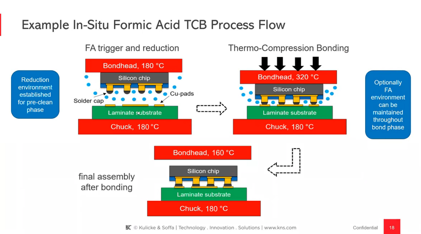
In response, the industry is transitioning towardfluxless TCBsolutions, aiming to increase interconnect density and quality without compromising bonding yield. Fluxless TCB eliminates the need for chemical flux and instead usesplasma activation,surface cleaning, andreducing atmosphere heatingto remove copper oxide layers. With precise thermal and pressure control, direct Cu-Cu bonding is achieved without reflow, resulting in a cleaner, more stable process—particularly beneficial for high-reliability packaging architectures.
Fluxless TCBis essentially a solderless, high-temperature/high-pressure bonding technique that enables Cu-to-Cu interconnects between chips and substrates. Compared to traditional TCB using flux or micro-bumps, and reflow soldering, fluxless TCB avoids residual contamination, mitigates bump-related failures, and enhances overall bond quality and system-level reliability.

Kulicke & Soffa (K&S)has introduced this fluxless TCB approach through itsAPTURA™platform. The platform has been validated forTSMC’s CoWoS-Lstandard and demonstrates stable Cu-Cu bump-less bonding performance. Furthermore, K&S has collaborated with academic partners to showcase that Fluxless TCB can be a viable alternative to hybrid bonding, supporting atomically aligned interconnects for high-density designs.
BESI, while primarily focused on its hybrid bonding platforms, is also actively collaborating withApplied Materials (AMAT)to develop the next generation of TCB solutions. These solutions aim to support fluxless bonding for high-bandwidth memory and AI IC stack integration, strengthening BESI’s position across chiplet, CoWoS, and SoIC platforms with vertically integrated packaging capabilities.
Heller, a leader in thermal processing systems, offers both traditional and fluxless reflow furnaces. Although not directly involved in TCB operations, Heller’s precision-controlled temperature profiles and convection systems support fluxless bonding environments by ensuring uniform thermal delivery and repeatability—critical for clean and robust bonding quality.
In summary,Fluxless TCBrepresents a major advancement over conventional TCB and reflow soldering by reducing contamination, improving process stability, and enabling high-reliability, high-density interconnects—making it one of the foundational technologies for the next generation of advanced packaging lines.
CoWoS-L and the Critical Role of Fluxless TCB in Advanced Packaging
As AI chip designs demand ever-greater bandwidth and integration,TSMC’s CoWoS-Lpackaging technology has emerged as a flagship solution for high-performance systems. CoWoS-L is tailored for multi-chip integration of large chiplets (e.g., logic dies) and HBM stacks. It places extreme requirements on chip alignment, bonding reliability, and thermal performance. Under these demands,Fluxless TCBhas become a pivotal enabling technology.
Fluxless TCB achievesdirect metal bonding, typically Cu-to-Cu, between die-to-die (D2D) or die-to-wafer (D2W) interfaces under controlled temperature and pressure, without any flux. This method avoids void formation and contamination associated with flux residues, thereby enhancing yield and long-term reliability. For CoWoS-L applications—where ultra-fine pitch, high current density, and low latency interconnects are critical—Fluxless TCB provides low resistance and high-bandwidth transmission while lowering overall power consumption.
Compared to traditional TCB with flux and reflow—which often requires multiple cleaning steps—Fluxless TCB simplifies the process and is better suited for advanced packaging environments wherezero contamination is tolerable. In CoWoS-L stacks, where HBM dies and large logic chips are integrated, the use of flux can cause entrapment of air bubbles, particles, or chemical residues between layers, affecting heat dissipation and signal integrity. Fluxless TCB effectively mitigates these risks.
Currently, several key equipment suppliers are offering solutions that support Fluxless TCB within the CoWoS-L packaging ecosystem:
Kulicke & Soffa (K&S): TheAPTURA™ Fluxless TCBsystem is widely adopted in high-precision packaging, offering ±1μm alignment accuracy. K&S works closely with TSMC on CoWoS-L production lines.

BESI and Applied Materials (AMAT): This partnership is driving an end-to-end TCB and hybrid bonding ecosystem targeting both HBM and logic die stacking, addressing mechanical, thermal, and interconnect challenges.
Heller: Although not directly providing TCB bonding tools, Heller suppliesfluxless-compatible reflow furnacescapable of tuning thermal profiles for specific bonding workflows, especially in custom integration environments.
In essence, CoWoS-L is not just a continuation of 2.5D packaging—it represents a transition toward3D high-integration and chiplet-based architectures. Its success relies heavily on high-precision, high-reliability interconnect methods such as Fluxless TCB. As chip sizes, bandwidth requirements, and power densities continue to rise, Fluxless TCB is set to play an increasingly central role in advanced packaging roadmaps.
From a supply chain perspective, the adoption of Fluxless TCB also fosters deeper collaboration acrossequipment vendors, foundries, and materials suppliers, accelerating innovation for AI chip integration and next-generation high-performance computing platforms.
Fluxless TCB and Hybrid Bonding in Advanced Packaging: Strategic Insights from TSMC, K&S, BESI, and ASMPT
As advanced packaging technologies grow increasingly complex and precise,Thermo-Compression Bonding (TCB)andHybrid Bondinghave emerged as pivotal techniques for integrating high-bandwidth memory (HBM) and logic chips. However, differing application scenarios and material systems across various packaging platforms have led to divergent equipment selections and process strategies.
For example, inTSMC’s CoWoS-Lplatform, theChip-on-Wafer (CoW)stage has officially adoptedKulicke & Soffa (K&S)’s fluxless TCB system for mass production. This system enables die attach without the use of flux, thereby avoiding residue-related contamination. However, because fluxless processes have relatively limited tolerance for tin bump oxidation,TSMC has implemented its own proprietary cleaning and activation processesto ensure consistent bond quality. This highlights TSMC’s stringent standards in process cleanliness and yield control.
In contrast,BESIhas concentrated its efforts onHybrid Bonding, a fundamentally different approach that does not involve flux or solder. Hybrid Bonding simultaneously bondsCu-to-Cu and dielectric layers(such as SiO₂ or polymer), and is widely used in high-density heterogeneous integration packages—such as logic-memory stacking—offering ultra-low parasitic characteristics and high-speed data transmission. BESI currently leads the market in this field, especially indie-to-wafer (D2W)bonding, with itsDatacon seriesplatforms adopted by multiple major fabs.
Meanwhile,ASMPToffers a range of TCB systems that include support forfluxless, no-solder Plasma-Activated Hybrid Bonding. This technology employs plasma treatment to increase surface energy and enable direct low-temperature metal bonding. It differs from traditional solder-based TCB and does not require flux, reflow, or flux cleaning steps.
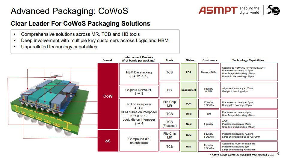
In summary,Fluxless TCB and Hybrid Bonding are not direct competitors, but rather complementary solutions tailored to different packaging contexts and material requirements. TSMC’s strategy in CoWoS-L shows that for cases where tin bump usage is still necessary, fluxless TCB—when combined with high-standard cleaning processes—remains a viable and effective approach. However, as the industry moves away from solder and towardhigh-density, flux-free interconnects, BESI’s Hybrid Bonding solutions demonstrate both technological superiority and market leadership. Moving forward, as chip size and packaging density continue to increase, bonding technologies will be evaluated based on theirintegration flexibility, scalability, and yield performance, making them central to next-generation packaging competitiveness.
Z-Height Control and the Equipment Race for Fine-Pitch Packaging
As advanced packaging platforms such asCoWoS-L,HBM stacking, andAI chiplet integrationcontinue pushing the limits of interconnect density and alignment precision, traditional TCB tools withoutaccurate Z-height controlare increasingly unable to meet production requirements. Atbump pitches below 40μm, even the slightest error in pressure or alignment height during bonding can lead to failures, shorts, or long-term reliability degradation.
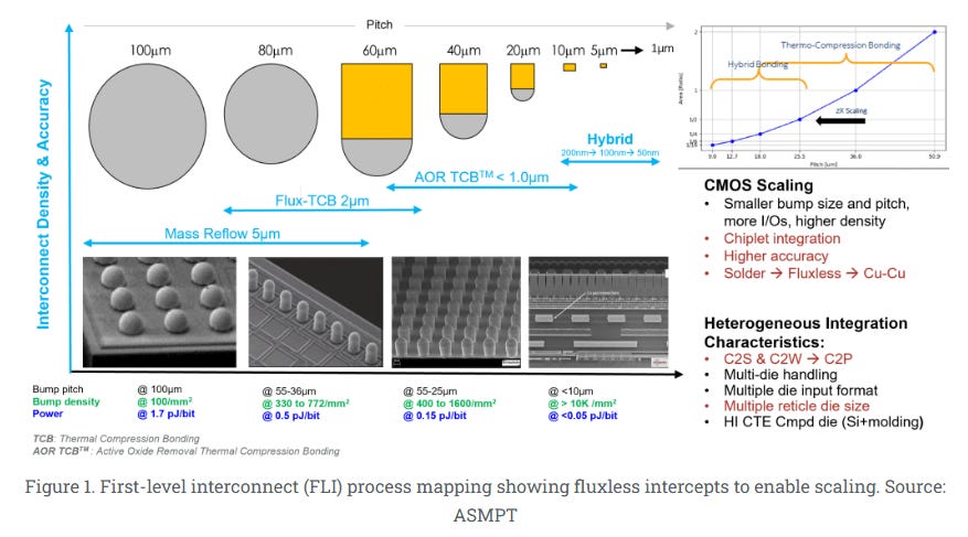
Furthermore, compared to leading suppliers likeBESI and ASMPT, many traditional TCB systems stilllack full integration with hybrid bonding workflows and heterogeneous die attach processes, limiting their applicability in cutting-edge packaging environments. While these TCB tools may still serve roles inimage sensor packagingor legacy applications, their limitations in Z-height precision and process flexibility make them increasingly unsuitable for future demands in AI, high-bandwidth memory, and optoelectronic integration.
As the market shifts towardmore advanced, highly integrated bonding platforms, those capable of supporting bothfluxless micro-bump attachment and hybrid bondingunder strict process controls will define the future of advanced packaging manufacturing.
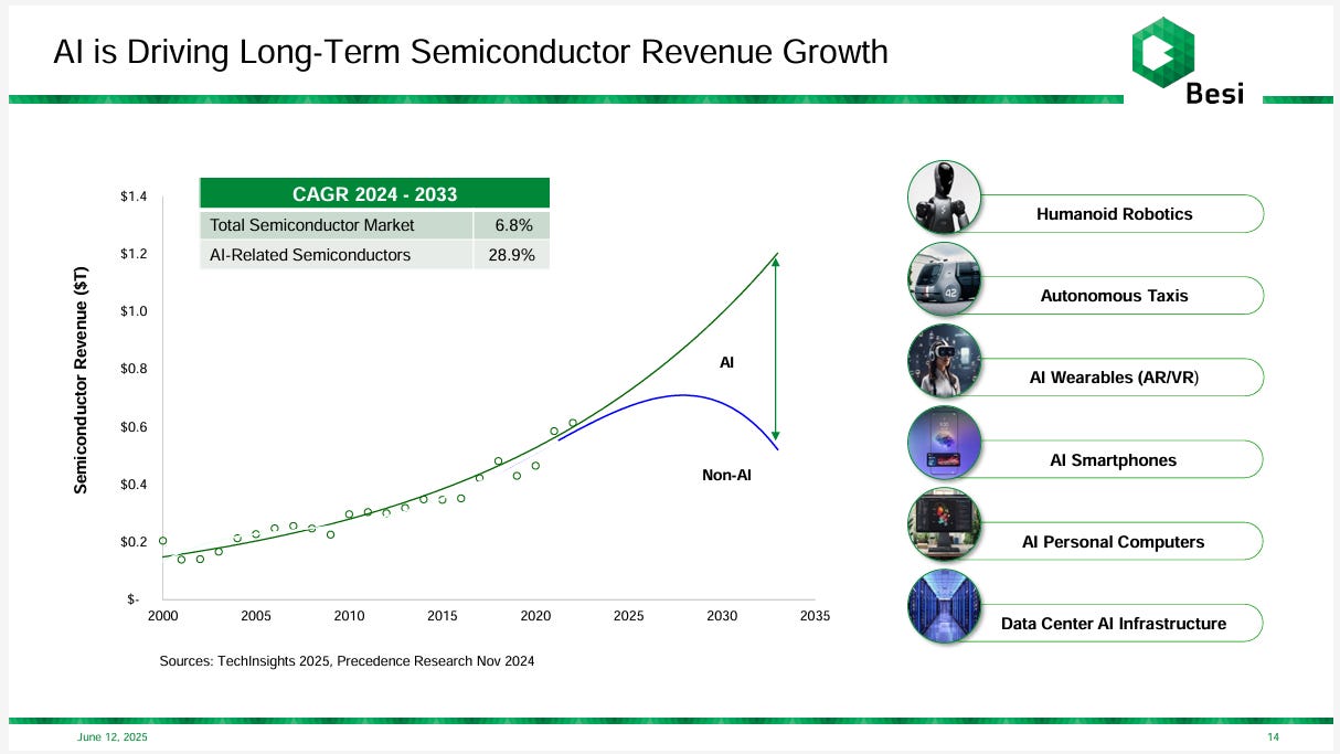
AI as the Primary Growth Engine for the Semiconductor Industry: BESI’s Outlook and Market Strategy
According to projections from TechInsights (2025) and Precedence Research (2024), Artificial Intelligence (AI) is poised to become the primary driver of global semiconductor revenue growth over the next decade. In its latest investor presentation, BESI highlights that AI-related semiconductors are expected to grow at a 28.9% CAGR, significantly outpacing the overall industry’s average growth rate of 6.8%, with the market size potentially exceeding $1 trillion by 2033.
Structural Divergence Between AI and Non-AI Semiconductor Markets
Market trend data clearly indicates astructural divergence: while the non-AI semiconductor segment is approaching maturity with slowing or stagnant growth, AI-related demand continues to surge exponentially. This shift reflects more than just the growth of GPUs or AI accelerators—it signals a broader transformation insystem architecture, driven by requirements inAI computation, memory bandwidth, high-speed interconnects, and advanced packaging.
As large-scale AI models evolve fromtens of billions to trillions of parameters, demand forAI SoCs,chiplet-based modular integration,HBM stacking, andCPO-enabled packagingis expected to rise sharply, offering equipment vendors like BESI substantial long-term opportunities in both technology leadership and revenue expansion.
Seven Key Application Segments Driving AI Semiconductor Demand
BESI identifiesseven core application segmentsthat will fuel future semiconductor demand in the AI era:
Humanoid Robotics
Requires highly integrated logic, sensor fusion, and ultra-low latency chips—demanding advanced packaging andhybrid bondingcapabilities.
Autonomous Taxis
Integrate AI vision, inference, and communication chips with requirements forhigh-frequency, low-power, multi-function ICs.
AI Wearables (AR/VR)
Energy-constrained devices requirechiplet-based architecturesthat tightly integrate GPUs, ISPs, sensors, and memory, raising packaging complexity.
AI Smartphones
With onboard AI for voice, image, and translation, the need forhigher logic density and memory bandwidthis accelerating the shift toultra-compact, high-density packaging.
AI PCs
Bring generative AI to endpoint devices through multi-accelerator and flash memory integration, necessitatingflexible heterogeneous packagingsolutions.
AI Data Center Infrastructure
The primary demand driver, requiringmassive AI accelerator modules,HBM stacking,CPO packaging,low-latency modular interconnects, andinnovative cooling solutions—an investment hotspot for next-generation advanced packaging equipment.
BESI’s Positioning: Targeting the Core of AI-Driven Growth
In response to this structural shift, BESI is strategically aligned with the technological demands of AI-centric applications through its platforms in:
High-precision Die Attach
Hybrid Bonding
Fluxless Thermocompression Bonding (TCB)
CoWoS and Fan-out Assembly
Wafer-level Packaging (WLP)
Whether forminiaturized, high-complexity consumer devicesorhigh-density, high-throughput AI datacenter modules, BESI’s equipment offers a competitive edge inprecision, flexibility, and scalability. As the packaging complexity of AI chips continues to increase, BESI is ideally positioned to capitalize on the resulting industry transformation.

BESI Focuses on Four Key End Markets: AI-Driven Architecture Driving Broad-Based Equipment Demand
According to BESI’s June 2025 strategic presentation, the company’s advanced assembly and packaging equipment has established a strong presence across four major end markets:Computing, Mobile Internet, Automotive,andIndustrial/Other. These four segments are projected to account for84% of BESI’s 2024 revenue, each propelled by megatrends inAI, sensing, connectivity, and sustainability.
- Computing – Largest Segment (43%)
BESI’s largest market is driven by high-performance computing (HPC) and AI training workloads. Key subsegments include:
Agentic AI:The rapid deployment of large language models (LLMs), AI agents, and multimodal inference systems has fueled demand for chip packaging solutions such ashybrid bonding, CoWoS, chiplet modular integration, andhigh-bandwidth memory (HBM) stacking.
AI-Enabled PCs:The rise of AI PCs is pushing system packaging toward integratedGPU/NPU/SoCarchitectures, increasing reliance oncompact, multilayer assembly platforms.
Silicon Photonics:With data centers and AI infrastructures accelerating the adoption of optical I/O, BESI’shigh-precision bonding and optical integration equipmentplay a key role in enabling next-gen photonic-electronic packaging.
- Mobile Internet – 20% of Revenue
BESI also supports the mobile ecosystem, driven by smartphones and wearable technologies:
AI Smartphones:Generative AI features such as smart imaging, translation, and voice assistants are now integrated into handsets, necessitatinghigher packaging densitiesand advanced module integration.
AR/VR Headsets:Mixed reality wearables demandlightweight, low-power, high-performance packaging, emphasizing 3D stacking and tight component integration.
Evolution to 6G:As wireless standards evolve beyond 5G, RF chip and antenna module packaging will demand higher density and integration, driving growth inFOWLP, WLP, and system-in-package (SiP) assembly solutions.
- Automotive – 12% of Revenue
In the automotive sector, BESI’s equipment addresses applications in both electrification and autonomous technologies:
Autonomous Driving:AI chips for real-time inference and multi-sensor fusion requirehigh signal integrity,power efficiency, andthermal performance—areas where BESI’s platforms excel inheterogeneous integrationandhigh-precision module assembly.
Vehicle Electrification:EV drive units and battery management systems requirereliable power packaging, with growing demand forthermocompression bondingandfluxless assembly.
Infotainment & Connectivity:Automotive-grade AI chips increasingly demandthin, high-frequency communication and vision modules, combining compact form factors with robust electrical and thermal performance.
- Industrial / Other Applications – 9% of Revenue
This segment captures a wide range of emerging applications that benefit from advanced packaging:
Robotics:Industrial and humanoid robots leverageheterogeneous chip modulesandintegrated sensor cores, increasing dependency on modular, high-reliability packaging platforms.
Smart Grid & Clean Energy:Power control ICs and management chips used in energy systems demandhigh thermal reliability, where BESI’s expertise inhigh-temperature bondingis a clear differentiator.
Industrial IoT:Embedded sensors and edge devices requireultra-compact, energy-efficient, and ruggedpackaging solutions, driving demand for BESI’s scalable assembly technologies.
BESI’s Equipment Portfolio Is Embedded Across the Entire AI Ecosystem
From hyperscale data centers to mobile devices, wearables, autonomous vehicles, and smart factories,BESI’s packaging and assembly solutions are integral to the AI system stack. Asagentic AIand thechiplet ecosystemexpand rapidly, packaging requirements now encompass not just logic dies but alsomemory, optics, and heterogeneous modules.
BESI’s upstream role in the equipment supply chain is evolving intoa central position in the construction of next-generation intelligent computing platforms. This deep, pervasive integration model provides astructural growth advantage, supporting long-term revenue expansion and market share leadership.
A New Paradigm Beyond Moore’s Law: BESI Drives Chiplet and 3DIC Packaging Revolution with Hybrid Bonding and TCB
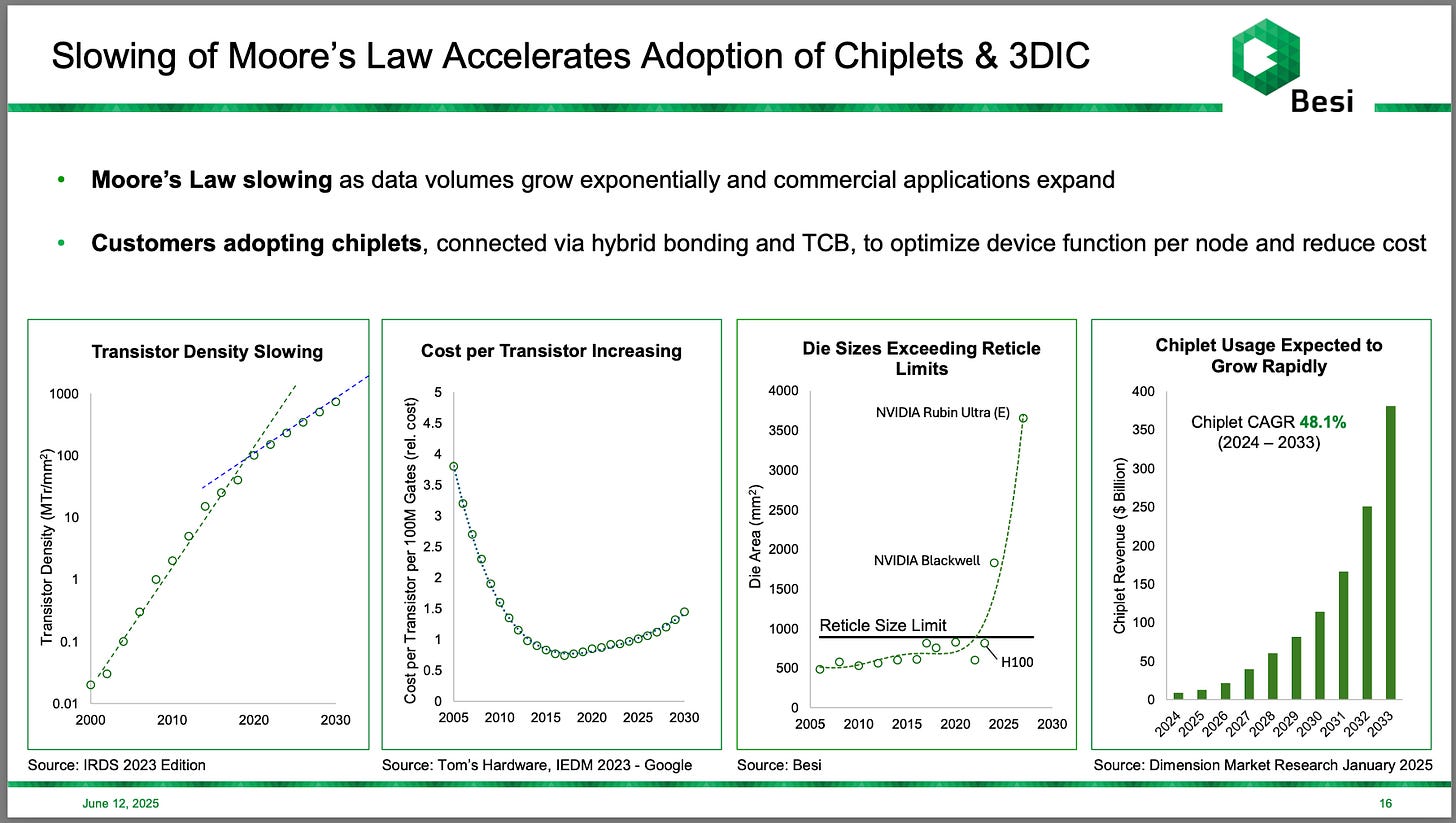
As Moore’s Law slows, semiconductor design and manufacturing are undergoing a paradigm shift. With physical scaling hitting fundamental limits, cost-per-transistor trends reversing, and chip sizes exceeding reticle constraints, the industry is moving towardchiplet architectures, 3DIC, and heterogeneous integration. BESI, a global leader in precision assembly and bonding equipment, is at the forefront of this transformation by advancingHybrid BondingandThermo-Compression Bonding (TCB)technologies. These innovations enable new performance, cost, and scalability frontiers in AI and high-performance computing (HPC) applications.
I. Three Structural Inflection Points in the Post-Moore Era
Transistor Density Growth Decelerates
According to the IRDS 2023 roadmap, the annual transistor density growth rate has significantly slowed since 2020—well below the historical 20-year average. This erosion of scaling benefits undermines the traditional SoC’s ability to gain performance through node migration alone.
Cost Per Transistor Is Rising
Reports from IEDM and Google reveal that, beyond the 5nm and 3nm nodes, wafer costs and packaging complexity are driving a reversal in the historical cost-down trend. This creates margin pressure for chip designers and favors disaggregation strategies.
Die Size Exceeds Reticle Limits
Flagship chips such as NVIDIA’sBlackwellandRubin Ultrahave surpassed single-reticle die limits, necessitating chiplet partitioning and reconstitution via advanced interposers. Equipment providers must now supportsub-micron alignment,micron-level bonding accuracy, andmulti-layer packaging stacking.
II. The Rise of Chiplets: Core Roles of Hybrid Bonding and TCB
BESI plays a critical role in enabling the chiplet era through advanced equipment solutions:
Hybrid Bonding

Anticipated to become a €1.2B market by 2030, hybrid bonding is a key enabler for HBM stacking, logic-memory heterogeneous integration, and 3D SoC design. BESI’s high-precision hybrid bonders deliver <50nm alignment accuracy, with core innovations including:
Surface treatment and oxide control for Cu-Cu bonding
Advanceddie placement with vision-based alignment systems
Warpage management andactive thermal controlfor ultra-thin dies (<50μm)
Fluxless Thermo-Compression Bonding (TCB)
BESI’sTCB Nextplatform supports fluxless bonding forHBM4/HBM5, Chip-on-Wafer, and wafer-level stacking. It improves bond strength, uniformity, and contamination control in memory and logic modules.
Advanced CoWoS Packaging
To support modular AI chiplet designs, BESI is enhancing its assembly platform with1μm placement precision, Flip Chip capability, andfine-pitch interconnect support, ensuringSerDes signal integrityandoptical module couplingconsistency.
III. Explosive Growth Trajectory: 48.1% CAGR in Chiplet Market
According to Dimension Market Research (Jan 2025), the global chiplet market is projected to surge from$2 billion in 2024to nearly$40 billion by 2033, reflecting a48.1% CAGR. Key growth drivers include:
AI model training demands massiveHBM + multi-NPU chiplet configurations
Modularization ofFPGAs, ASICs, and SerDesfor cost-effective design and risk mitigation
Custom AI accelerator initiatives fromhyperscalerslike AWS and Google
Adoption ofCXLandoptical interconnects, driving protocol-level chiplets into packaging workflows
BESI is expanding itsHybrid BondingandTCB product linesto precisely address chiplet assembly requirements, yield optimization, and integration complexity. The company is strengthening collaborations withIDMs(Intel, TSMC, Samsung) andfabless leaders(NVIDIA, AMD, Broadcom), securing its position as a strategic enabler of the next generation of semiconductor systems.
A New Paradigm for Data Center Chips: Chiplet Architecture and Hybrid Bonding Go Mainstream
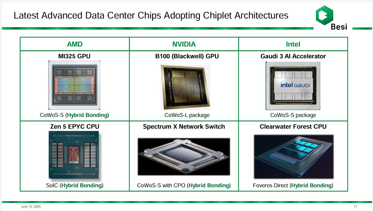
As generative AI scales, data volumes explode, and power efficiency hits its limits, semiconductor architecture is undergoing a fundamental transformation. Across accelerators, CPUs, networking chips, and optoelectronic components, leading chipmakers are rapidly adoptingchiplet-based modular designandhybrid bondingto enablelarge-area packaging, mixed-node integration, andhigh-speed interconnects. BESI’s platform roadmap confirms this trend, showing that AMD, NVIDIA, and Intel have fully transitioned their flagship 2024–2025 data center chips toward chiplet and advanced packaging architectures—marking a turning point in semiconductor evolution.
AMD: Dual Platform Strategy with CoWoS-S and SoIC
AMD exemplifies aggressive modularization across its data center product line:
MI325 GPU: Built onTSMC’s CoWoS-S platformand enhanced withhybrid bonding, this architecture allows sub-micron alignment of GPU tiles and HBM stacks. The result is lower I/O latency and improved energy efficiency.
Zen 5 EPYC CPUs: EmployTSMC’s SoIC (System on Integrated Chips)with hybrid bonding to vertically integrate logic chiplets with I/O dies. This achieves denser heterogeneous integration and better power management.
By leveraging bothSoIC and CoWoSplatforms, AMD has successfully unified performance scaling with high-bandwidth memory integration—delivering flexible design architectures across compute workloads.
NVIDIA: Extending CoWoS into the Optoelectronic Era
Under theBlackwell architecture, NVIDIA is pushing packaging innovation further:
B100 GPU (Blackwell): UsesCoWoS-L, a large-area, high-bandwidth packaging platform integrating multiple logic dies with HBM stacks. While not explicitly stated, hybrid bonding is likely part of this tightly stacked configuration.
Spectrum-X Network Switch: A pioneering platform combiningCoWoS-SandCo-Packaged Optics (CPO)withhybrid bonding. This is the industry’s first example of integrating optical modules directly with a switch chip, addressing the demand for ultra-low-latency, high-bandwidth interconnects in data centers.
NVIDIA’s strategy demonstrates that packaging is no longer limited to compute chips—it is also the key enabler for future optical and communication convergence in AI systems.
Intel: Disaggregated Integration with Foveros and CoWoS
Intel is taking a hybrid IDM-foundry approach with differentiated strategies:
Gaudi 3 AI Accelerator: Manufactured usingTSMC’s CoWoS-S, this marks a strategic shift as Intel adopts third-party advanced packaging for its AI lineup—highlighting its open ecosystem model to remain competitive.
Clearwater Forest CPU: Relies on Intel’s proprietaryFoveros Directplatform, ahybrid bonding-based 3D stackingtechnology. Foveros enables vertical integration of memory, logic, and I/O modules, reducing interconnect length and power consumption.
By deploying bothFoveros and CoWoS, Intel targets complementary market segments—CoWoS for AI accelerators and Foveros for its next-generation x86 CPUs.
Packaging as the Core Weapon for Chip Differentiation
The chip industry is undergoing a structural shift wherechiplet-based modularization and hybrid bondingare becoming foundational to next-generation high-performance platforms. From x86 CPUs and GPUs to AI ASICs and network switches, chipmakers are no longer constrained by monolithic SoC scaling. Instead, they are overcoming reticle limits, bandwidth bottlenecks, and power delivery challenges through advanced integration.
BESI’s hybrid bonding and die-attach technologiesare at the heart of this transformation, enabling precision alignment and high-yield stacking for logic-memory-optical co-design. The data center of the future will be shaped not by transistor count alone, but by theinterplay of packaging strategies, modular integration, and interconnect efficiency—a battlefield where BESI continues to play a mission-critical role.

AMD Leads the Chiplet Revolution: From Data Centers to Gaming Desktops
As semiconductor nodes advance below 5nm, the cost of wafer fabrication has surged exponentially. According to BESI, a 2nm wafer is projected to cost over $25,000—several times more than a 28nm wafer. Under this economic pressure, traditional monolithic chip designs are becoming increasingly unsustainable due to yield limitations and diminishing commercial viability.Chiplet architecturehas emerged as a compelling alternative—offering superior cost efficiency, design flexibility, and scalability.AMD stands at the forefront of this paradigm shift.
Hybrid Bonding: Unlocking Performance and Power Efficiency
AMD’s Chiplet strategy is not merely about modular design; it represents a bold evolution towardheterogeneous integration and 3D stacking. In the Zen 5 architecture, AMD vertically stacks compute chiplets atop SRAM chiplets usinghybrid bonding. This directcopper-to-copper (Cu-Cu)interconnect approach replaces traditional micro-bumps and underfill adhesives, significantly reducing signal delay and impedance while minimizing thermal resistance and volume. The result is enhancedhigh-frequency performance,lower power consumption, andsub-micron alignment accuracy.
Five Core Advantages of Chiplet Architecture
AMD’s product roadmap clearly highlights the following systemic benefits of Chiplet design:
Improved Yield and Cost Efficiency
Smaller chiplets have lower defect rates compared to large monolithic dies, improving overall yield and reducing scrap losses.
Enhanced Power Efficiency
Shortened data paths and reduced memory distances lead to lower power consumption and better thermal design performance (TDP).
Design Flexibility
Enables mixed-node integration (e.g., 4nm + 6nm) for targeted performance tiers and product segmentation.
Faster Time-to-Market
Modular design allows parallel development and rapid iteration—accelerating deployment.
Scalability
Supports flexible core and I/O scaling to meet a wide range of workload requirements.
Diverse Deployment: From EPYC to Ryzen
AMD has successfully deployed this strategy across multiple product lines:
AI Data Centers – EPYC 9004 Series
Features multiple CCDs (Core Complex Dies) stacked on a large I/O die with hybrid bonding, delivering massive bandwidth and multi-core performance for LLM inference and training workloads.
General-Purpose Servers – EPYC 4585PX
Targets cloud and enterprise environments using the same Chiplet platform to balance performance and efficiency.
Consumer Desktops – Ryzen 9 9900X3D
Combines a 4nm compute die with a 6nm SRAM chiplet, leveraging3D V-Cachetechnology to dramatically boost gaming cache and performance, while optimizing power and latency.
BESI and AMD Define the Future of Packaging Innovation
BESI is more than an equipment supplier—it plays a pivotal role in transforming semiconductor manufacturing and packaging design. Through itshigh-precision hybrid bonding platforms, BESI empowers AMD and other advanced players to realize the full potential of chiplet architectures. From data centers to edge computing and consumer electronics, this synergy is reshaping the landscape of high-performance semiconductor systems.
As process scaling approaches physical limits and costs escalate, the fusion ofChiplet architecture and hybrid bondingis emerging as the cornerstone of continued innovation in the semiconductor industry.

Accelerating Die Attach Innovation for Multi-Chip Systems: From Monolithic Integration to 3D Chiplet Packaging
As Moore’s Law slows and process costs surge, semiconductor design has shifted from monolithic SoC architectures to modular,chiplet-based systems. While this evolution enables design flexibility and cost control, it also introduces unprecedented challenges for backend assembly—particularly indie attachprocesses. In its latest briefing,Besiunderscores that chiplet adoption is reshaping the demand landscape for advanced die bonders and redefining the packaging process flow.
Three Generations of Chip Integration Paradigms
Single Chip Design
Traditional SoCs integrate all functional subsystems on a single die. Die attach occurs once, requiring around±10μm alignment precision, with relatively simple equipment requirements.
Multi-Chip Modules (MCM)
Modular designs distribute CPU, GPU, and I/O onto separate dies optimized for different process nodes. Die attach now involvesmultiple operations, each needing tailored pressure, temperature, and alignment control.
3D Multi-Chiplet Systems
Further advancement integrates diverse functional IPs (compute, memory, control) in vertically stacked configurations forheterogeneous integration. This can requiretens of die attach steps, with alignment precision targets approaching<100nm, pushing equipment accuracy and optical alignment to new limits.
Emerging Technical Challenges in Die Attach for 3D Chiplets
With chiplet-based designs comprisingdozens of discrete dies, the die attach process must evolve from basic bonding to acomplex integration workflow. Key challenges include:
Sub-Micron Alignment & Thermal Drift Compensation
Addressing tool expansion and chiplet dimensional variation caused by thermal cycling during bonding.
Stacking Stress & Warpage Control
Advanced 3D structures are prone to warpage. This demands preciseZ-axis motion,real-time force sensing, and active planarity correction.
Material and Bonding Method Integration
Compatibility with next-generation bonding methods such asthermocompression bonding,hybrid bonding, andlaser-assisted bondingis essential.
Multi-Level Test and Inspection
Integration ofKGD (Known Good Die) validation, in-linethermal sensors,automated optical inspection (AOI), andre-pick & re-placefunctions to improve yield and traceability.
Besi’s Strategic Role in the Next Era of Die Attach
As packaging progresses from 2.5D totrue 3D integration, and asheterogeneous and optoelectronicsystems become mainstream, die attach must evolve into a multidisciplinary convergence ofoptics, thermomechanics, materials science, andautomated control software.
Besi, a global leader in die bonding and hybrid bonding equipment, is at the center of this transformation. Its platforms are not only designed for high-precision placement but also enable:
Sub-100nm alignment repeatability
Scalable throughput to support high-volume manufacturing (HVM)
Outlook: Die Attach Becomes Strategic in the AI and HPC Chip Supply Chain
With chiplet architectures gaining momentum acrossAI,high-performance computing (HPC), andadvanced networking, the market for next-generation die attach systems is poised for exponential growth. Besi’s key opportunity lies in developing a platform that delivers:
Support for dozens of die-to-die operations per package
High throughput with minimal placement error
Field-upgradable modules for hybrid bonding and fluxless TCB
Process intelligence for yield learning and automation
Diverse Integration Demands of AI Chiplet Packaging: Besi’s Perspective on Advanced Packaging Evolution
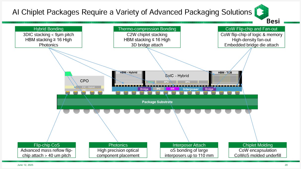
As AI and HPC chips push the limits ofintegration density,energy efficiency, anddata transfer latency, traditional packaging approaches are no longer sufficient to meet the performance demands of system-level integration. In its 2025 technical briefing,Besiunveiled a comprehensive framework for advanced packaging, illustrating how the realization ofheterogeneous integration,3D stacking, andoptoelectronic co-packaginghinges on the orchestration of multiple bonding and assembly technologies.
Three Core Bonding Technologies for Next-Gen AI Packaging
Hybrid Bonding
Regarded as thecornerstone for AI and high-speed memory packaging, hybrid bonding offerssub-10μm pitchand superior electrical conductivity. Key applications include:
3D IC stacking(sub-9μm pitch)
High-stack HBM(up to 16+ layers)
Optoelectronic integration, such asphotonic enginesand co-packaged optics
Thermo-Compression Bonding (TCB)
Suited forChip-to-Wafer (C2W)assembly and bridge die stacking for HBM architectures (≤16 layers). TCB enables stable mechanical joints under pressure and temperature, ideal for high-speed memory-to-logic interconnects.
Chip-on-Wafer (CoW) Flip-Chip & Fan-Out
Used for dense memory-to-logic I/O coupling:
Supportsembedded bridge dieto boost channel density
Fan-outredistributes I/O space to accommodate larger system-in-package (SiP) modules
Seven Packaging Modules Required for AI Chiplet Platforms
Beyond bonding, a complete AI chiplet integration flow must include a variety ofplatform-level processes:
Flip-Chip CoS (Chip-on-Substrate)
Traditional reflow process supporting >40μm pitch; enables high-throughput production alignment for large-scale logic die.
Photonics Alignment
High-precision optical device placement critical for minimizing loss insilicon photonics modulessuch asCPOandoptical switchesin AI datacenters.
Interposer Attach
Enables attachment oflarge interposers (up to 110mm)used in SoIC, CoWoS, and other dense packaging platforms. Demands exceptional planarity and adhesive uniformity.
Chiplet Molding & Underfill
Reinforces mechanical stability and manages thermal expansion, particularly for CoW structures. Essential for robustness during multi-die encapsulation.
Bridge Die Integration
For passive or active inter-die connectivity, often embedded to minimize latency and improve routing.
Thermal & Warpage Compensation Systems
Ensures integrity of high-stack dies through thermal modeling and stress-reducing molding compounds.
Optical-Electrical Co-Packaging Infrastructure
For cases involvingCPO modules, packaging must integrate high-speed optics and RF shielding in a single platform, demanding sub-micron alignment and loss budgeting.
System-Level Integration Challenges in the Chiplet Era
With elements such asSoIC,XPU architectures,IVRs,bridge dies, andCPO photonicsconverging into a single package, advanced packaging has shifted from a mechanical enclosure to aplatform-level enabler. Today, packaging solutions must fulfill roles in:
Signal integrity optimization
Thermal dissipation
Bandwidth scaling
Photonic-electronic interfacing
Besi’s system-level packaging cross-section reveals thatAI chip innovationis no longer driven solely by process scaling—but by packagingco-evolution. Every component—fromHybrid BondingtoCPO alignment—demandscapital-intensive,precision-oriented, andhigh-reliability equipment, highlighting the strategic growth role of packaging equipment suppliers over the next decade.

Accelerating the Era of AI Packaging: A Comprehensive View of BESI’s Advanced Packaging and Chiplet Architecture Solutions
As Moore’s Law slows, the semiconductor industry is rapidly transitioning towardchiplet-basedand3D heterogeneous integration architectures.BESI, a key player in advanced packaging equipment, is leveraging its comprehensive technology portfolio to support evolving demands from datacenters, high-performance computing (HPC), artificial intelligence (AI), and complex system integration. This article dissects BESI’s positioning and technological trajectory through five critical lenses:strategic focus,R&D investment,chiplet architecture transformation,AI-driven packaging demand, andequipment platform expansion.
- Strategic Focus and Technology Leadership: R&D-Centered Growth in Advanced Packaging
BESI is strategically focused onhigh-value, high-growth packaging segments, emphasizingR&D leadershipover market share. Key strategic pillars include:
Continuous enhancement of technology leadership
Expansion intowafer-level packaging (WLP)
Addressable market enlargement through chiplet-driven opportunities
Acquisition of complementary technologies
Commitment to2030 sustainability goals
Rather than pursuing volume for its own sake, BESI prioritizes high-value partnerships with leading-edge customers, tailoring its capabilities to applications requiringflexibility, performance, and yield control.
- R&D Investment and Process Technology Breakthroughs: Entering the Sub-Micron Era
Between 2019 and 2024, BESIdoubled its R&D expenditure, reaching 13% of revenue. Key areas of focus include:
50nm-precision hybrid bondingsystems
CoWoS packaging platformsfor AI/HPC
Evolution of theEvo platform to 1μm precision
Advanced support forFlip-Chip,TCB, andphotonics packaging & inspection
These investments directly address the exponential growth in AI hardware demands and strengthen BESI’s leadership position in next-generation semiconductor packaging.
- AI and Chiplet Architecture: Driving Packaging Innovation
Between 2024 and 2033, AI semiconductor CAGR is projected at28.9%, significantly outpacing the overall semiconductor growth rate of 6.8%. Growth is fueled by:
Human-assistive robotics and autonomous systems
AI smartphones, AR/VR wearables
AI-enabled PCs and hyperscale datacenter infrastructure
BESI identifieschiplet architecturesas key to unlocking post-Moore system scalability, enabling better trade-offs incost, yield, power, and flexibility. Major industry players likeNVIDIA, AMD, and Intelhave fully embracedCoWoS, SoIC, Foveros, andhybrid bondingin their latest AI and HPC chips, signifying a mainstream shift toward 3D stacked integration.
- From Design to Equipment: BESI’s Advanced Packaging Platform Portfolio
To meet the rising complexity of packaging structures, BESI has built a robust equipment lineup spanningdie alignment,bonding,interconnect,molding, andphotonics integration. Representative solutions include:
8800 CHAMEO UltraPlus AC: Hybrid bonding (<9μm pitch), photonics alignment, HBM stacking
9800 TC Next: Thermo-compression bonding (supports 16-high HBM and 3D bridge integration)
8800 CHAMEO Flex: CoW flip-chip and dense fan-out packaging
8800 Quantum AdvX: Flip-chip CoS for >40μm pitch interfaces
2200 Evo 1μm / Advanced: High-precision photonics and 110mm interposer bonding
xMS-NXT: Chiplet molding platform (in development)
These platforms are compatible with today’s CoWoS-L/S and SoIC ecosystems and are scalable for futurefine-pitch,multi-layer, andheterogeneous photonic-electronic integrations.
- Packaging Challenges and Process Transformation: Raising Barriers, Increasing Value
As chiplet designs proliferate, die attach has evolved from asingle-step processto dozens of precision alignment stages, reducing tolerances from10μm to sub-100nm. This disrupts traditional SoC assembly and imposes stringent demands onequipment accuracy, throughput, andprocess control. BESI addresses these challenges with targeted solutions:
Hybrid Bonding: For 3D IC stacking, photonic modules, and HBM integration
Thermo-Compression Bonding (TCB): For mid-level HBM stacks and bridge dies
Flip-Chip CoS: For high-speed interface modules with large pitch
Interposer Attach: For ultra-large-area base platforms
CPO and Photonics Packaging: Entering thesub-micron precisionbonding regime
BESI’s Critical Role in the AI Packaging Transformation
BESI’s packaging strategy is systematic, forward-looking, and strongly aligned with the evolving landscape of AI, HBM, and 3D heterogeneous integration. With the chiplet market projected to grow at48.1% CAGR between 2024 and 2033, BESI is uniquely positioned to drive innovation inhigh-density packaging, modular architectures, fine-pitch manufacturing,andoptoelectronic convergence.
Through its cutting-edge platforms and R&D leadership, BESI is not just supplying tools—it is enabling theinfrastructure for the AI computing revolution.

Hybrid Bonding: The Preferred Technology for High-Performance Chiplet Stacking
In advanced logic chiplet architectures, traditionalThermo-Compression Bonding (TCB)andmicro-bumpinterconnect technologies are increasingly limited by constraints ininterconnect density, power consumption, and bandwidth—rendering them less suitable for cutting-edge AI and HPC designs. In contrast,Hybrid Bondinghas emerged as theindustry’s front-runnerfor enabling true 3D IC integration withsub-10μm interconnect pitches, making it the most promising solution for next-generation high-performance chip stacking.
Compared to conventionalChip-to-Wafer (C2W) TCBbonding, Hybrid Bonding offers overwhelming advantages across key metrics:
15x increase in interconnect density, significantly reducing package footprint and signal path length.
~12x higher signal transmission speed, ideal for high-speed SerDes and stacked AI memory modules.
Up to 191x increase in bandwidth density, enabling support for significantly more channels and I/O interfaces.
Over 100x improvement in Energy Efficiency per Performance (EEP), reducing power consumption in AI inference and training scenarios.
Comparable interconnect cost per unitto TCB, while delivering performance gains by orders of magnitude—making it more cost-effective as yield and volume scale.
Hybrid Bonding is now widely adopted in leading-edge platforms, includingAMD’s SoIC,Intel’s Foveros Direct, andTSMC’s 3DFabric. Its core innovation lies incopper-to-copper (Cu-Cu)anddielectric-to-dielectricdirect bonding, eliminating the need for intermediate micro-bumps. This allowsatomic-level contact, reduced parasitics, and higher mechanical reliability.
In this context,Besi’s 8800 CHAMEO UltraPlus AC Hybrid Bonderhas been engineered to support such ultra-fine-pitch interconnects. It is also extendable toPhotonic IC stackingandHBM vertical integration, positioning Besi as a central enabler in the transformation of AI chip manufacturing.

Intel Leverages Hybrid Bonding to Drive Next-Gen Datacenter Processors
With the launch of itsClearwater Forestdatacenter processor in 2025,Intelhas fully embracedHybrid Bondingtechnology, marking a major milestone in its pursuit of 3D stacking and chiplet-based architectural innovation. Built on theIntel 18A process node, the Clearwater Forest processor integratesup to 12 CPU chiplets, vertically bonded onto a base tile comprisingSRAM and I/O functionalities, forming a high-performance, high-density 3D structure.
This architectural breakthrough, internally referred to asFoveros Direct, represents an evolution from Intel’s originalFoveros heterogenous integration platform. Foveros Direct enablesatomic-level bonding accuracyandmodular partitioning of functional blocks, redefining the possibilities of system integration. Leveraging Hybrid Bonding, Foveros Direct achievesinterconnect densities exceeding 10,000 bumps per mm², dramatically shortening the physical distance between CPU cores and SRAM. The result isreduced latencyandimproved memory access efficiency.
Pushkar Ranade, Intel Vice President, commented:
“3D stacking shortens the hops between compute and memory, enabling lower latency and larger integrated cache capacity.”
This design philosophy underpins the Clearwater Forest platform’s massive integration, withover 300 billion transistorsacross its architecture.
Intel’s adoption of Hybrid Bonding reflects a strategic commitment toredefining its datacenter chip platform, optimizingperformance, energy efficiency, anddie area utilizationthrough 3D integration. At the same time, it lays the technical groundwork for thenext generation of modular, chiplet-based platforms, signaling a clear path toward the future of compute.

Hybrid Bonding Enters Pre-Mass Production Phase with Broadcom and Apple Leading the Way
As AI and high-performance computing (HPC) markets accelerate, more semiconductor design companies are adoptingHybrid Bondingto overcome performance bottlenecks. The latest developments fromBroadcomandApplesignal that industry acceptance of 3D chiplet stacking and advanced packaging has progressed beyond proof-of-concept and is now on the cusp ofhigh-volume manufacturing (HVM).
Broadcomrecently announced the completion of the world’s first3.5D Face-to-Face (F2F) packaging platformtailored for AI XPU designs. This platform combines the advantages of3D silicon stackingwith2.5D interposer-level integration, and is expected to utilizeTSMC’s SoIC processto implement Hybrid Bonding. Initial production will start with6µm bonding pad pitch, targeting custom AI ASICs for clients such asGoogle, Fujitsu, Apple, andOpenAI. Mass production is expected by2026, enabling the next generation of XPUs to achieve higher bandwidth, lower latency, and superior energy efficiency.
Meanwhile,Appleis incorporating Hybrid Bonding into its upcomingM-series chip roadmap. TheM5,M5 Pro/Max, andM5 Ultraare scheduled for production inearly 2025,late 2025, and2026, respectively. These chips will debut withserver-grade SoIC-mH (Molding Horizontal)packaging, a design that modularizes the CPU and GPU into separate dies, tightly integrated viaTSMC’s SoIC platform. This modular approach enhances thermal management, improves yield, and allows for greater architectural flexibility.
Apple’s move marks a strategic shift from highly integrated SoCs toward amodular, heterogeneously integrated packaging paradigm, withHybrid Bonding as the enabling foundation.
Taken together, Broadcom and Apple’s adoption of Hybrid Bonding not only highlights the technology’s compatibility with cutting-edge AI and compute workloads, but also signifies a pivotal transition fromlab validation to mass deployment. AsTSMC’s SoIC platform, along with material and equipment ecosystems, reach maturity, equipment vendors likeBesiare expected to play a critical role in scaling up this new packaging frontier.

Hybrid Bonding Unlocks Value in Emerging CPO Applications
As data centers evolve toward ultra-high bandwidth and energy-efficient architectures,Co-Packaged Optics (CPO)is emerging as a foundational technology for next-generation switches and AI accelerators. Recent developments byNVIDIAandBroadcomillustrate how Hybrid Bonding is becoming essential for achieving compact, high-reliability electro-optical integration in CPO platforms, while also accelerating supply chain scalability.
NVIDIA’slatestSpectrum-X Ethernet switchesandQuantum-X800 InfiniBand seriesincorporate up to36 optical engine chiplets, eachtightly bonded to the switching ASIC using Hybrid Bonding techniques. These devices are fabricated usingTSMC’s COUPE platform(Co-Packaged Optics Using Embedded Photonics Elements) in combination withSoIC F2F (Face-to-Face)packaging, enabling seamless vertical integration ofElectronic ICs (EICs)andPhotonic ICs (PICs).
TheCOUPE architectureintegrates multiple layers—supporting silicon interposers, microlens arrays, and metal reflectors—to achievesub-micron optical alignmentwithout compromising electrical performance. This hybrid packaging approach dramatically reduces signal paths, enhances thermal performance, and improves system reliability, paving the way for large-scale deployment of CPO-based interconnects.
Broadcom, on the other hand, has demonstrated a CPO switch engine withmulti-layer flip-chip interconnectsandPIC-EIC vertical stackingembedded within the substrate. This hybrid architecture complements emerging Hybrid Bonding techniques and is already deliveringlow-power, high-reliability interconnect solutionsfor hyperscalers likeGoogle, Meta, andAmazon.
According toYole’s 2025 market report, shipments of CPO optical engines are projected to grow at aCAGR of 100% through 2035, marking a shift toward explosive adoption. Such growth will demand proportional expansion of Hybrid Bonding capacity, withsignificant capital investment and production line scalingrequired by 2030 to meet volume demands.
These flagship implementations and market forecasts reinforce thatHybrid Bonding is no longer a premium option—it is now the foundational technology for AI and optical data center integration. Its role inenabling high-yield, cost-effective, and scalable CPO moduleswill be central to the industry’s transition. Consequently,key enablers like Besi and TSMCare poised to gain even greater strategic importance in shaping the next phase of semiconductor packaging and photonics manufacturing.
Reshaping the AI Chip Packaging Era: From Hybrid Bonding to the Full Evolution of the Chiplet Architecture
As demand for generative AI and high-performance computing (HPC) surges, data center chips are pushing packaging technologies to their limits with unprecedented complexity and power efficiency challenges. Traditional monolithic SoC (System-on-Chip) designs can no longer cope with the cost pressures and design flexibility requirements of advanced process nodes. This shift has prompted leading players—AMD, NVIDIA, and Intel—to fully embrace chiplet architectures and heterogeneous integration. At the heart of this packaging revolution liesHybrid Bonding technology, which is increasingly pivotal in enabling 3D stacking, high-bandwidth memory (HBM), and photonic integration (CPO) in high-performance scenarios.
Chiplet Adoption Trends Driven by Three Major Players
Among today’s flagship products:
AMDadoptsCoWoS-S and SoIChybrid bonding technologies for its MI325 GPU and Zen 5 EPYC CPU, enabling high-density logic and memory stacking.
NVIDIAimplements a hybridCoWoS-L + CPOpackaging approach in its Blackwell B100 GPU and Spectrum-X switches, highlighting energy efficiency and modularity.
Intel, with itsGaudi 3 AI acceleratorandClearwater Forest CPU, usesFoveros Directto vertically stack logic, SRAM, and I/O chiplets. These products exceed 300 billion transistors, marking a new benchmark for future logic-stacked platforms.
Chiplet Architectures Drive New Demands for Packaging Equipment
Compared to traditional SoCs that require a single die attach step, modern 3D multi-die systems demand dozens of high-precision bonding operations, with alignment precision moving from 10μm down to below 100nm. This presents both challenges and opportunities for equipment vendors likeBesi, across areas including Hybrid Bonding, thermo-compression, flip-chip bonding, photonic alignment, and interposer integration.
Besi’s Comprehensive AI Chiplet Packaging Solutions
Besi offers a full lineup of tools for various stacking technologies, including:
8800 CHAMEOfor Hybrid Bonding
9800 TC Nextfor thermo-compression bonding
8800 Quantum AdvXfor Flip-chip CoS
2200 evo seriesfor photonic and interposer alignment
xMS-NXTmodular molding platform for advanced packaging R&D
These systems support cutting-edge requirements from TSMC, Intel, and SK hynix, and are capable of handling pad pitches as small as 6μm.
Hybrid Bonding vs. TCB: A Clear Technical Advantage
According to analyses by TSMC and Besi, Hybrid Bonding outperforms traditional copper-to-wafer thermo-compression bonding (C2W TCB) in nearly every key metric:
15xinterconnect density
~12xspeed improvement
191xbandwidth density
Over 100xenergy efficiency
Superior cost control
Clearwater Forest and Foveros Direct: New Technical Milestones
Intel’s 2025Clearwater ForestCPU, built on the 18A node with 12 core chiplets, leveragesFoveros Directfor 3D integration. It represents a scalable high-bandwidth, low-latency x86 platform with massive on-die cache. Key innovations include:
10,000/mm² copper interconnect density
Function-block-level partitioningin 3D stacking
These mark a fundamental shift in chip and memory architecture integration.
Mass Production Momentum for New Hybrid Bonding Applications
Broadcomleads the industry with its first3.5D Face-to-Face (F2F)hybrid package, leveraging TSMC’s SoIC platform to develop AI ASICs for OpenAI, Google, and Fujitsu—targeting mass production in 2026.
Appleis also expected to adoptserver-grade SoIC-mHpackaging for its M5 Pro/Max/Ultra chips. This involves separating CPU and GPU into modular dies, enhancing thermal performance and yield.
CPO and Photonic Integration Drive a Packaging Revolution
In theCo-Packaged Optics (CPO)domain,NVIDIAandBroadcomboth utilizeTSMC’s COUPE platformand Hybrid Bonding to integrate up to36 photonic chipletsper switch module. This enables:
Ultra-high bandwidth
High module density
Increased equipment demand
Yoleforecasts CPO optical engine shipments will grow at a100% CAGRfrom 2024 to 2035, signaling an explosive new growth frontier in advanced packaging.
HBM Stacking Roadmap and Besi’s Opportunities
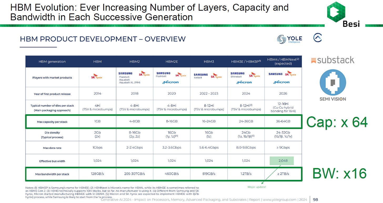
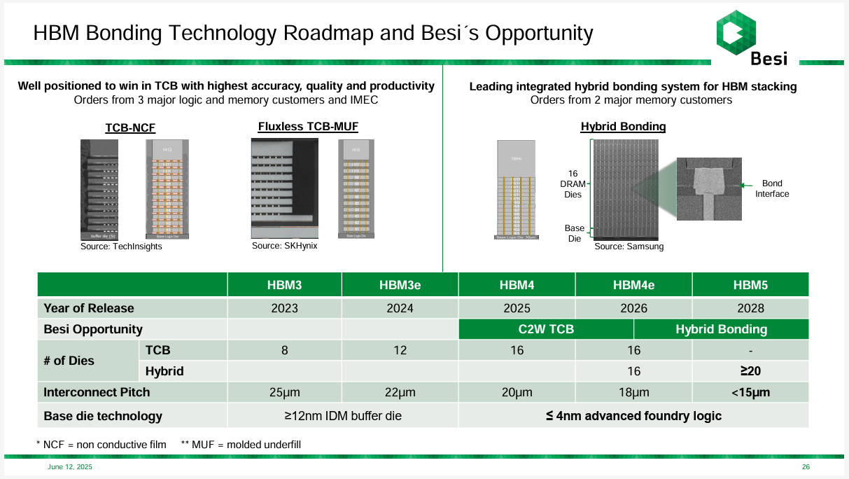
WithHBM3 and HBM3ein production, Besi is rapidly entering theHBM4 and HBM5markets. Orders from major DRAM vendors for Hybrid Bonding systems are secured.
HBM5will feature over20 stacked layers, <15μm contact pitch, and <4nm logic base dies
These specifications push bonding precision, thermal design, and throughput to new extremes
Packaging as a Platform—Hybrid Bonding Shapes the Future of AI Chips
AI chip design is no longer about stacking compute cores alone. It now spans memory, photonics, power delivery, and data interfaces into a unified system platform. Within this paradigm shift,Hybrid Bondingis not merely an option but a foundational technology for realizing chiplet integration, reducing power, and boosting bandwidth.
With its comprehensive equipment portfolio,Besihas secured its strategic position at the forefront of next-generation AI chip packaging.
Hybrid Bonding: Unlocking the Future of HBM and Logic Integration
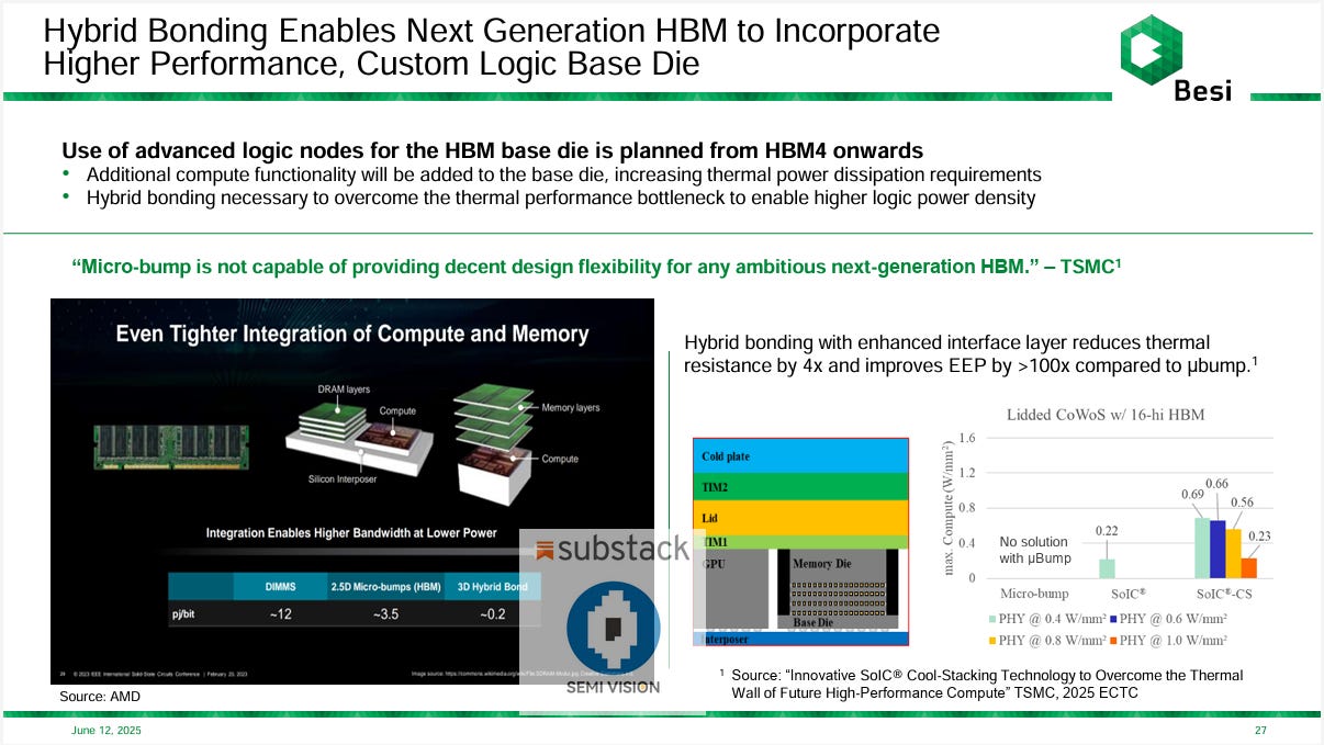
TSMC has explicitly stated:“Micro-bump technology can no longer support the design flexibility required by next-generation HBM.”In architectures that stack more than 16 layers of DRAM and incorporate high-power logic on the base die, conventional bump-based stacking suffers from excessive thermal resistance and signal latency—failing to meet the growing power and bandwidth demands of AI accelerators.
Hybrid Bondinghas emerged as a key enabler in this context. Unlike micro-bump stacking, hybrid bonding enables near-atomic-level copper-to-copper direct connections, reducing thermal resistance by up to4×and improvingEnergy Efficiency Performance (EEP)by more than100×. According to data from AMD and TSMC, a traditional DIMM system consumes around12 pJ/bitfor data transfer, while a 2.5D micro-bump HBM stack requires3.5 pJ/bit. In contrast, a 3D hybrid-bonded architecture can push this down to under0.2 pJ/bit, representing a dramatic leap in efficiency.
Moreover, TSMC’s 2025 ECTC presentation on itsSoIC and SoIC-CSpackaging platforms further highlights how hybrid bonding, combined with enhanced thermal interface layers (TIM1 and TIM2), significantly contributes to compute density. Under a power density of 1.0 W/mm², conventional micro-bump stacked designs can only sustain0.22 W/mm²of effective compute density. In comparison, SoIC and SoIC-CS architectures reach0.66and0.69 W/mm²respectively—and potentiallyexceed 0.8 W/mm²with more advanced cooling solutions.
These findings illustrate thatHybrid Bonding is not merely a packaging option, but a foundational technologyenabling the transformation of HBM into a programmable logic-memory integration platform—ushering in the era ofin-memory compute. For AI-driven architectures focused on training and inference, Hybrid Bonding offers a path to simultaneously optimize bandwidth, latency, and power—setting the stage for a new era in advanced 3D packaging.

Smartphones Embrace Chiplet Packaging: A Dual Revolution in AI and Advanced Packaging
As generative AI (GenAI) steadily permeates consumer applications, smartphones are approaching a pivotal architectural transformation. According to TSMC and IDC’s July 2024 projections, the compound annual growth rate (CAGR) for AI smartphones between 2024 and 2028 is expected to reach an impressive41.4%, far outpacing the2.2%CAGR of traditional smartphones. This wave of AI-driven demand is accelerating parallel advancements in chip design and packaging technologies. At the heart of this transformation lies thechiplet-based architectureandadvanced packagingfor next-generation AI Processing Units (APUs).
Currently, most mainstream smartphone APUs still utilizemonolithic System-on-Chip (SoC)packaging architectures, including Apple’sInFO PoP, and Qualcomm and MediaTek’sMCP/MCEpplatforms. However, to meet the growing demands for AI inference—particularly compute power and memory bandwidth—mobile SoCs are shifting towardchiplet-based architectures. Through2.5D and 3D integration, multiple smaller dies can be assembled onto wafer-level redistribution layers (RDL), enablingheterogeneous integration,thermal-power balance, and higherlogic density.
Future architectures such asCoW-RandSoIC X/Pare expected to enter mass production between2027 and 2028. These will leverage Besi’sCHAMEO flex,TC Next, andHybrid Bondingplatforms to execute flip-chip assembly, TCB (thermocompression bonding), and direct hybrid bonding processes. Compared to conventional mobile packaging, these approaches supporttighter pitch dimensionsandhigher bandwidth density, significantly boosting SoC capabilities inAI processing,NPU performance, andmemory access speed.
Yole Development forecasts that by2030, the annual shipment volume of mobile and consumer electronic devices featuring3D SoIC packagingwill exceed300 million units, signaling explosive growth. This trend will not only restructure the packaging equipment and materials supply chain, but alsoreshape SoC design paradigms—shifting from large monolithic dies tomodular, multi-die, and flexible packaging models.
In this evolution, smartphones are poised to become theleading consumer product linedriving chiplet packaging into the mass market. This will unlock unprecedentedeconomies of scaleandinnovation opportunitiesfor wafer-level packaging and heterogeneous integration platforms.

Overview and Trends of Hybrid Bonding Technology
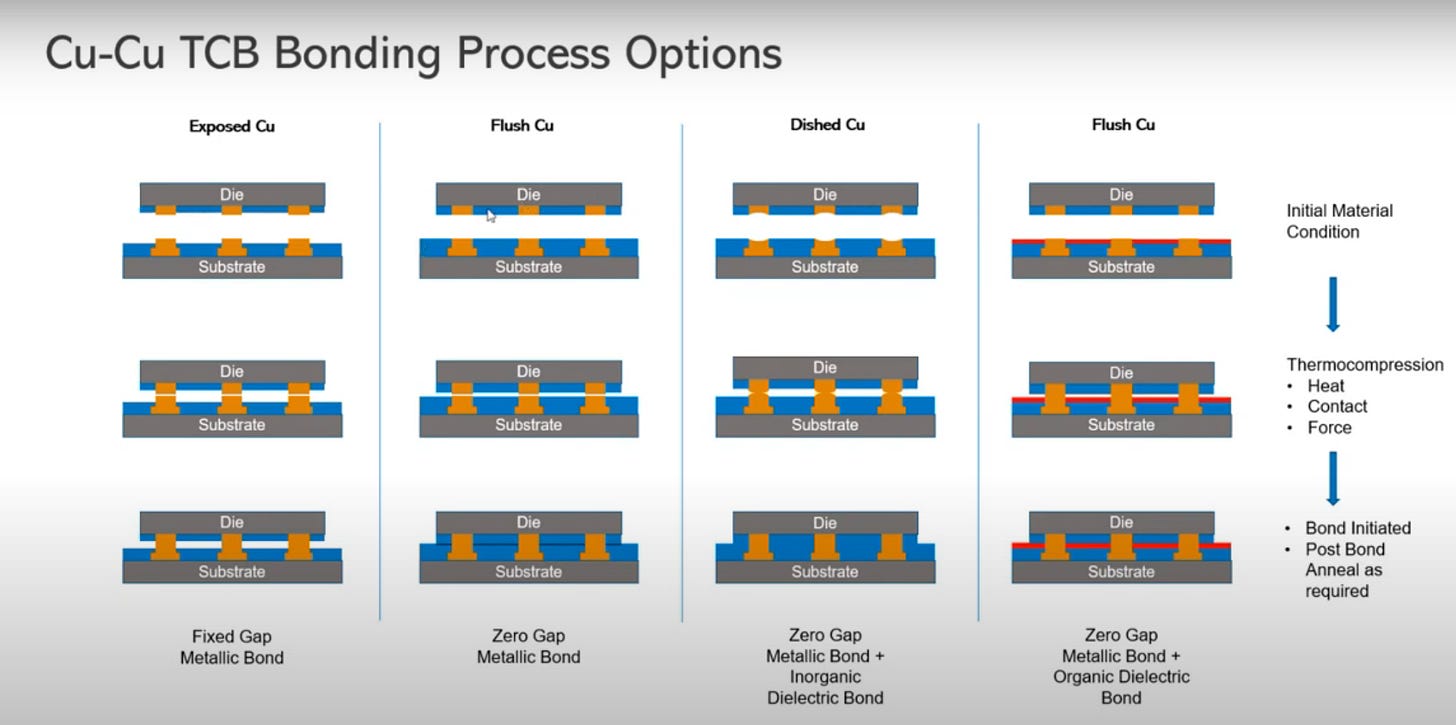
Hybrid bonding is a high-density packaging technology that enables face-to-face, copper-to-copper direct interconnects at the chip or wafer level, significantly enhancing packaging density and performance. Compared to traditional wire bonding, solder bumps, or through-silicon vias (TSVs), hybrid bonding allows direct alignment and bonding between chip layers, achieving interconnect pitches at the micron or even sub-micron scale. For example, its interconnect density can be tens of thousands of times higher than conventional micro-bump bonding, while substantially reducing parasitic resistance, capacitance, and inductance—thereby improving signal transmission speed and reducing power consumption.
In addition, the hybrid bonding process involves fewer steps (around 11), reducing complexity and cost compared to traditional bump-based bonding. Because the bonding interface is solid-state and embedded, it also helps minimize thermal gradients within chip stacks, improving overall thermal stability in multilayer integrated devices. These advantages make hybrid bonding highly attractive for advanced memory, high-frequency sensors, and heterogeneous integration applications.
For instance, in the image sensor sector, Sony has reportedly applied hybrid bonding to more than 90% of its CMOS image sensor products. Multiple NAND flash manufacturers—such as YMTC, Kioxia, and Western Digital—are actively adopting hybrid bonding processes. Since 2022, AMD has integrated the technology in its 3D SoCs to combine high-bandwidth memory (HBM) with logic circuits. Industry analysts expect rapid growth in the hybrid bonding market, with TechInsights forecasting a jump from around USD 26 billion in 2024 to USD 112 billion by 2029, representing a compound annual growth rate (CAGR) of approximately 28%.
Hybrid bonding delivers near-monolithic performance with ultra-low power consumption, making it a key enabler for next-generation 3D packaging in high-performance computing (HPC), artificial intelligence (AI), data centers, and 5G communications.
Hybrid bonding enables direct copper-to-copper bonding between chip layers, with interconnect densities up to tens of thousands of times higher than traditional micro-bump methods. This dramatically improves signal transmission speed and reduces power consumption.
Compared to conventional packaging, hybrid bonding significantly reduces parasitic resistance, capacitance, and inductance, resulting in higher system bandwidth and lower energy consumption.
The hybrid bonding process also involves fewer steps—approximately 11 instead of dozens—making manufacturing simpler and more efficient.
Because the bonding interface is composed of solid-state conductive copper joints, it helps reduce internal thermal gradients within chip stacks, improving thermal performance and allowing multi-chip stacking with enhanced heat dissipation without compromising performance.
However, the hybrid bonding process presents significant challenges. First, it requires extremely high alignment accuracy—within tens of nanometers or better—to ensure complete copper pad bonding. Second, the bonding interface demands ultra-high cleanliness, requiring process conditions similar to front-end semiconductor fabrication standards (cleanroom environment, particle control, surface flatness) to avoid contamination-related bonding failures.
In addition, warpage and stress management for thin wafers and heterogeneous materials become more complex, necessitating precise thermomechanical control and advanced metrology to maintain bonding yield.
Overall, achieving near-zero-defect copper bonding interfaces requires stringent pre- and post-bonding treatments such as CMP, cleaning, and surface activation, and may also require modifications to both upstream (wafer processing) and downstream (packaging design) processes.
Wafer-to-Wafer (W2W) vs. Die-to-Wafer (D2W) Hybrid Bonding
Hybrid bonding can be classified into two main process types: wafer-to-wafer (W2W) and die-to-wafer (D2W).

W2W bonding refers to aligning and bonding two whole wafers, typically used when the die sizes are small or the wafers are of the same size. This method allows alignment and bonding to be decoupled, resulting in higher yields and lower particle contamination. However, its limitation is the inability to perform known-good-die sorting prior to bonding, potentially locking defective dies into the final structure.
D2W bonding, on the other hand, involves individually placing pre-tested (known-good) dies onto a target wafer. This ensures that only functional dies are bonded, but each transfer step introduces risks of contamination and more stringent process requirements.
Industry consensus suggests that W2W is more suitable for applications with small die areas and stable yields—such as image sensors or certain memory ICs—while D2W is better suited for larger dies, irregular shapes, or cases requiring high wafer yields, such as advanced SRAM/DRAM or AI SoCs.
According to EVG, W2W bonding is already mature in CMOS image sensors and various memory/logic stacking applications. However, for 3D systems involving heterogeneous die sizes, D2W is considered more practical. EVG further categorizes D2W into two modes:Collective Die-to-Wafer (Co-D2W)andDirect Placement Die-to-Wafer (DP-D2W).
InCo-D2W, multiple dies are pre-arranged on a carrier wafer and bonded collectively, achieving efficiency similar to large-area wafer bonding.
InDP-D2W, flip-chip bonding equipment is used to place dies one by one onto the base wafer, providing flexibility to accommodate varying die sizes and thicknesses.
In practice, many 3D packaging solutions—such as HBM memory stacking and heterogeneous SoCs—employ acombination of W2W and D2Wto balance yield and integration flexibility.
Latest Developments among Key Hybrid Bonding Equipment Suppliers
- BESI (BE Semiconductor Industries)
Global Leader in Precision D2W Hybrid Bonding and High-Yield Production Platforms
As one of the leading semiconductor assembly equipment providers, BESI is aggressively investing in hybrid bonding technology. Its flagship platform, the Datacon 8800 CHAMEO series—particularly the latest “8800 CHAMEO ultra plus AC”—achieves exceptional standards in cleanliness and alignment precision, enabling ultra-precise placement and high throughput. BESI also offers TCB Next for thermal compression bonding at 5-micron-level pitches, tailored for HBM and AI chip applications. During its FY2025 Investor Day, BESI announced a revenue target of €1.5–1.9 billion, fueled by the explosive growth in 2.5D/3D packaging demand driven by AI and 5G. Additionally, BESI has partnered with Applied Materials to develop an end-to-end hybrid bonding solution that integrates BESI’s precision die placement with Applied’s front-end thin film and etch processes. Orders related to hybrid bonding have increased significantly, particularly from Asian fabs for HBM4 and logic base die bonding, with Q1 2025 bookings growing over 8% quarter-over-quarter.
- EV Group (EVG)
Market Leader in Comprehensive Wafer Bonding and W2W Hybrid Bonding Solutions

EVG is a global leader in wafer bonding solutions, offering the most comprehensive hybrid bonding equipment portfolio. In wafer-to-wafer (W2W) hybrid bonding, EVG claims a market-leading position with its GEMINI platform, supporting up to four bond modules to achieve high-volume, high-quality bonding. For die-to-wafer (D2W) applications, EVG continues to expand its offerings. The GEMINI FB enables large-scale die bonding; the EVG®320 supports pre-bonding chip surface preparation and activation; and the EVG®40 NT2 metrology tool integrates AI-driven feedback for yield enhancement. Notably, EVG’s Heterogeneous Integration Competence Center demonstrated a 100% yield in multi-die 3D SoC bonding using GEMINI FB. EVG emphasizes that hybrid bonding requires front-end cleanroom standards, including ultra-clean plasma activation, advanced cleaning, and nanometer-level alignment—making it a pivotal enabler for mass production of AI and high-speed memory chips.
- Applied Materials (AMAT)
Process Giant for Hybrid Bonding with Front-End Integration and Materials Mastery

Applied offers critical process tools for every stage of hybrid bonding, including advanced thin film deposition, electroplating, and CMP. The Insepra™ SiCN coating system forms new interface layers for bonding, while Catalyst CMP performs ultra-precise planarization to ensure copper-to-copper bonding quality. Applied has partnered with key players to develop full process flows—collaborating with EVG on W2W hybrid bonding for image sensors and NAND, and with BESI on D2W bonding for logic-HBM integration. These partnerships enable seamless front-end and back-end integration, facilitating rapid process qualification and production ramp-up.
- Tokyo Electron (TEL)
End-to-End Solution Provider for Wafer Cleaning, Bonding, and Thin Wafer Processing
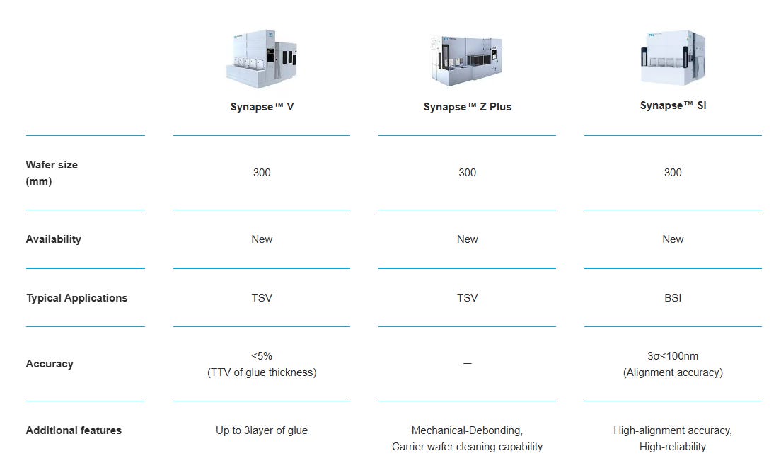
TEL offers a full suite of wafer bonding solutions through itsSynapse™ and Ulucus™ platforms.The Synapse series, an industry-standard for 300mm temporary bonding and debonding, supports TSV and CIS production. The new Synapse™ Si combines lens platform precision (from LITHIUS Pro Z) with integrated cleaning and plasma treatment, enabling permanent hybrid bonding for copper-to-copper applications. The Ulucus™ series supports ultra-thin wafer edge trimming and laser lift-off, integrating precise coating with post-bond processing for high-yield production. TEL expects a significant increase in demand for permanent bonding and has introduced automated, high-throughput tools targeting memory and AI chip mass production.
- ASM Pacific Technology (ASMPT)
Automation Pioneer in Cu-to-Cu Bonding and Scalable 3D Packaging Equipment

ASMPT, one of the largest global packaging equipment providers, has also entered the hybrid bonding arena. Its flagshipLITHOBOLT™ platformperforms fully automatic die-to-wafer bonding in ISO 3 cleanrooms, achieving solderless Cu-to-Cu connections on 12” wafers. The system supports top/bottom die bonding, scalable with multiple machines, and ensures consistency via fully automated control. ASMPT has partnered with leading companies such as EVG (for ultra-precision D2W bonding) and IBM (for bonding quality validation in AI chips). As chip designs transition to 3D integration, ASMPT expects LITHOBOLT™ to become a central enabler in advanced packaging.
- SET (Smart Equipment Technology)
Niche Expert in Ultra-High Precision D2W Hybrid Bonding Systems
France-based SET specializes in high-precision die placement and bonding. ItsNEO HB platformis dedicated to direct hybrid bonding (D2W), achieving ±0.5μm alignment accuracy (3σ) in ISO 3 cleanrooms. It supports room-temperature Cu bonding and flip-chip assembly, applicable to 5G/6G, memory stacking, and AI integration. CEA-LETI and Intel demonstrated bonding at 400nm accuracy and kUPH-level throughput using SET systems, showcasing their potential from lab to volume production.
- Shibaura Mechatronics
Early Commercializer of Hybrid and Fusion Bonding with Dual-Head High-Throughput Platforms

Shibaura’s TFC-6700 and TFC-6800platforms support Chip-to-Wafer hybrid and fusion bonding. Commercialized since 2016, these tools offer ultra-high positioning accuracy and ISO 1 cleanliness, adopted in GPU, HBM, and CIS markets. The dual-head TFC-6800 increases throughput by bonding two wafers simultaneously. Shibaura emphasizes its expertise in bonding precision and cleanroom control, meeting server and AI chip demand for ultra-dense bump-less integration.
- SUSS MicroTec
Innovator of Modular Bonding Solutions Supporting Both W2W and D2W Integration
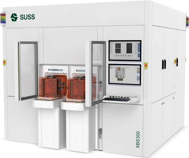
Germany’sSUSS MicroTecdeveloped the XBS/XBC hybrid bonding platforms. The XBS300 W2W bonder supports 200/300mm wafers with <100nm overlay and integrated metrology. The XBC300 Gen2, a versatile hybrid bonding cluster, supports both W2W and die-to-wafer (batch or single die) bonding. In 2024, XBC300 Gen2 was installed at the SkyWater/BRIDG Neovation Center in Florida, a public-private R&D hub for advanced bonding demonstration. SUSS highlights its bump-less bonding solutions to accelerate heterogeneous integration in production environments.
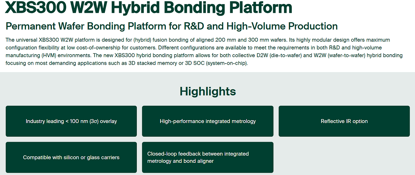
Hybrid bonding, which enables high-density, low-power 3D integration without TSVs or wire bonds, is increasingly adopted in GPUs, AI chips, 5G, and advanced memory. Despite the challenges in achieving sub-micron alignment and front-end-grade cleanliness, major equipment vendors have launched turnkey platforms and formed strategic alliances with semiconductor companies to scale production. As Moore’s Law slows, hybrid bonding is widely regarded as a cornerstone of next-gen heterogeneous packaging, with the market expected to grow rapidly in the coming years.


PreviousNext
TopLatestDiscussions








See all