Hybrid Bonding at Scale: BESI’s Vision and Industry Evolution in 3D Integration
Hybrid Bonding at Scale: BESI’s Vision and Industry Evolution in 3D Integration
- Source: SemiVision
- Author: SEMIVISION
- Published: 2025-07-11T10:29:58+08:00
- URL: https://tspasemiconductor.substack.com/p/hybrid-bonding-at-scale-besis-vision Hybrid Bonding at Scale: BESI’s Vision and Industry Evolution in 3D Integration


Hybrid Bonding at Scale: BESI’s Vision and Industry Evolution in 3D Integration
Original Articles By SemiVision Research ( IEEE ECTC , IEEE IITC ,BESI , TSMC , Nvidia, AMD , Intel ,TEL , Suss ,EVGroup , K&S , ASMPT ,AMAT , SHIBAURA ,SET , NYCU ,ITRI)

Jul 11, 2025
∙ Paid

As AI and high-performance computing (HPC) continue to advance rapidly, chip architectures are shifting toward 3D stacking, chiplet disaggregation, and heterogeneous integration. The realization of these technologies heavily depends on continuous breakthroughs and scalable mass production ofbonding technologies. In this field, one company has long held a critical position—BE Semiconductor Industries N.V. (Besi), based in the Netherlands.
Besi: A Key Driver of the Transition from Planar to 3D Advanced Packaging
Founded in 1995and headquartered in Duiven, the Netherlands, Besi operates manufacturing, R&D, and service facilities across Malaysia, China, Singapore, and the U.S. The company specializes in designing and manufacturing high-precision assembly equipment for the back-end semiconductor process, particularly targeting advanced logic chips, memory, sensors, and photonic devices.
Besi’s product portfolio spans from traditional 2D packaging to cutting-edge 2.5D and 3D packaging technologies, excelling in the following four core areas:
Besi’s Strategic Role in Advanced Packaging

Market Leadership
Besi holds a42% market sharein die-attach equipment, maintaining its global leadership for years. Its product offerings span epoxy, soft-solder, flip-chip, stacked die, and multi-module applications.
High Throughput and Precision Integration
Besi’s flagshipDataconandEsecplatforms deliver±4 μm @3σ precision, enabling high-speed, high-yield manufacturing with ultra-fine chip spacing—perfectly suited for performance-critical applications.
AI and Data Center Demand as Growth Catalysts
With the rise of AI, 5G, HPC, and chiplet-based modules, Besi’s advanced packaging solutions have become a critical enabler. InQ1 2025, Besi’s order intake increased by8.2% to €131.9 million, largely driven byhybrid bonding orders.
Hybrid Bonding: Besi’s Core Technological Contribution

https://www.besi.com/products-technology/product-details/product/datacon-8800-chameo-ultra-plus-ac/
Hybrid bonding is at the heart of Besi’s technology roadmap. As a key enabler of vertical chip stacking and high-density interconnects, it delivers lower latency, reduced energy consumption, and enhanced bandwidth/system performance.
Breakthrough Capabilities
<10 nm Alignment Precision: Besi’s tools enable atomic-level copper-to-oxide and oxide-to-oxide bonding, essential for 3D integration.
Thermo-Compression Integration: Platforms like8800 CHAMEO ultra plus ACcombine cleanroom-grade bonding and optical alignment to ensure high yield and tight pitch stacking.
Industry Collaboration and Market Penetration
In 2024, Besi received orders for hybrid bonding systems with 100 nm alignment capabilities, indicating readiness for next-generation nodes.
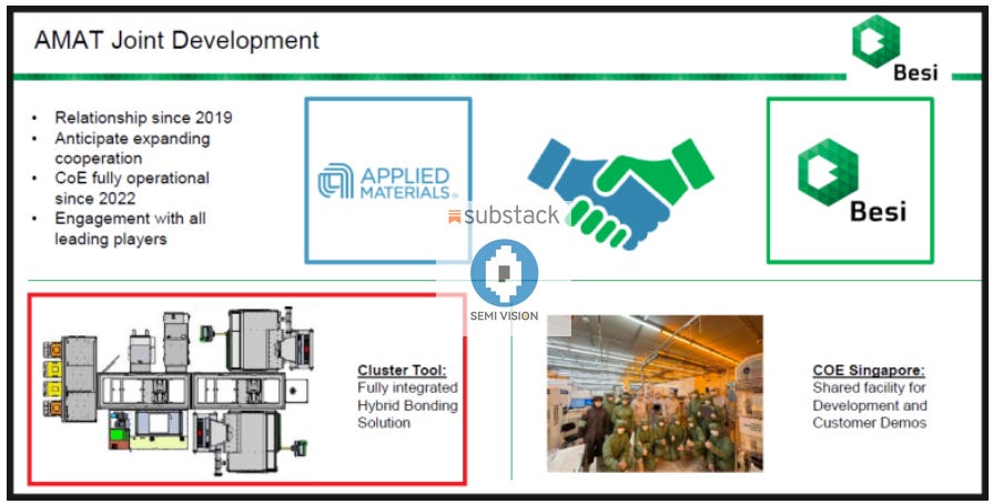
Strategic partnership with Applied Materials (AMAT) since 2020, deepening in 2025 as AMAT became Besi’s largest shareholder (9%), enabling tight integration from deposition to final assembly.

Financial Outlook and Strategic Significance
At its 2025 Investor Day, Besi elevated hybrid bonding to a core business pillar, raising long-term revenue targets to €1.5–1.9 billion with 40–55% operating margins.
Financial Times reported hybrid bonding revenues at €36M in 2023, projected to surge to €476M by 2026, potentially accounting for one-third of Besi’s total business.
Technology Leadership and Strategic Positioning
Besi leads the hybrid bonding segment with its exceptionalprecision (<10 nm), high-yield control, and ultra-fine interconnect density, positioning itself at the forefront of AI, HBM, and 3D-IC packaging innovations.
Together with Applied Materials and ASML, Besi is part of a vertically integrated supply chain pushing hybrid bonding into high-volume production.

Growth Trajectory
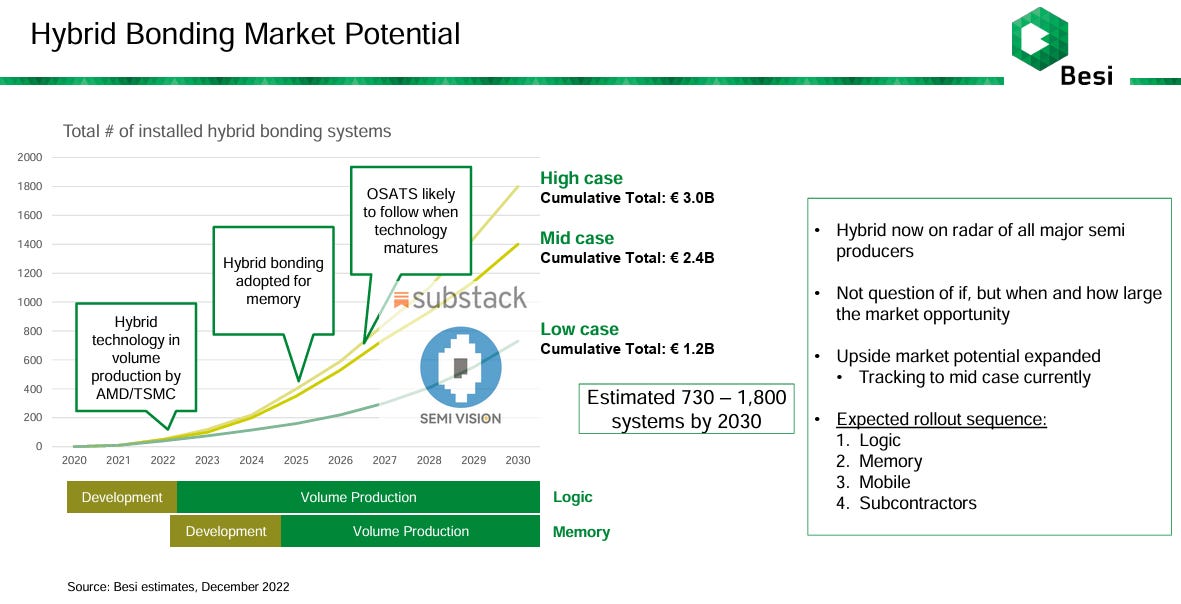
With increasing demand from AI infrastructure and data centers, Besi is successfully transitioning hybrid bonding from a niche technology into amajor revenue engine, showing strong long-term growth potential.
Why Should We Pay Attention to Hybrid Bonding Technology?
What Are the Challenges, and Where Is Advanced Packaging for AI Chips Heading?
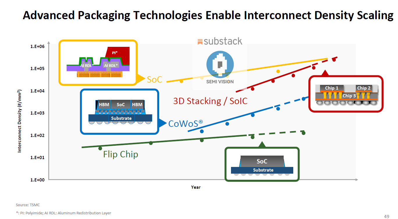
These are all critical questions worth exploring. TSMC, for instance, is actively advancing its SoIC technology, which is fundamentally a 3D stacking architecture. This reflects the industry’s broader shift toward higher levels of integration and performance.
Hybrid Bonding: A Core Enabler for the New Era of 3D Chip Design

Hybrid bonding is regarded as one of the most transformative innovations in semiconductor manufacturing since extreme ultraviolet (EUV) lithography. Not only does it significantly improve the precision and performance of chip stacking, but it also redefines how chip designers approach 3D architectures and system integration.
Whereas EUV focuses on scaling within a single die, hybrid bonding opens up a new dimension—literally—enabling vertical stacking of multiple dies. It has become an essential technology for the advancement of advanced packaging and high-performance computing.

In the semiconductor industry, bonding technology plays a pivotal role in enabling heterogeneous integration and high-density 3D stacking architectures. As 3D ICs, chiplet-based designs, and advanced packaging technologies continue to gain traction, traditional bump-based or solder reflow methods are increasingly insufficient to meet the demands of finer pitches and high-speed data transmission. In contrast, hybrid bonding, which involves wafer-to-wafer (W-W) or die-to-wafer / die-to-die (D-W / D-D) alignment and interconnect, has emerged as the mainstream solution driving high-performance computing (HPC), AI chips, and memory stacking.
According to Tokyo Electron (TEL), bonding technologies are now widely applied across various device types, including CIS image sensors, 3D NAND, DRAM, logic ICs, backside power delivery (PDN), sequential CFETs, and advanced packaging scenarios such as HBM and disaggregated chiplets. Each application demands different levels of bonding precision and interconnect pitch—from 40 µm for early-generation memory stacks down to sub-micron and even <1 µm interconnects for next-generation chiplet architectures.

In advanced packaging, hybrid bonding not only increases I/O density and improves signal integrity, but also enables low-power, high-bandwidth heterogeneous integration. It is the foundational technology behind major 3D packaging platforms such as TSMC’s SoIC, Samsung’s X-Cube, and Intel’s Foveros. Looking ahead, as logic and memory stacking become more tightly coupled and bandwidth requirements continue to rise, bonding technology will only grow in importance—serving as a key enabler of innovation at both the chip and system levels.
- Technical Principles and Architectural Characteristics
Hybrid bondingis a semiconductor stacking technology characterized by itsbump-lessinterconnect structure. Unlike traditional solder-based packaging, hybrid bonding achieves both electrical and mechanical interconnection throughdirect copper-to-copper (Cu-Cu) contact. The top and bottom chips are bonded tightly, with only ultra-fine patterned copper pads encapsulated in dielectric material between them. These Cu pads typically have pitches below 10 µm and connect to internal chip metal layers throughthrough-silicon vias (TSVs), forming complete signal and power paths.
The term “hybrid” refers to thecombination of dielectric-to-dielectric molecular bondingandmetal-to-metal copper bonding, both formed without adhesives. This results in a more stable, low-loss interface with excellent electrical and thermal properties.
- Technical Advantages and System-Level Benefits
Hybrid bonding provides numerous technological and system-level advantages that are fundamentally reshaping chip design and system architecture:
Ultra-high interconnect density: Enables vertical interconnects at sub-10 µm, even down to hundreds of nanometers, far exceeding the density of traditional bump-based approaches.
Low resistance and reduced power: Eliminating solder bumps significantly reduces interconnect resistance, enhancing energy efficiency and thermal performance—crucial for high-speed data paths.
Low latency and short interconnects: Dramatically shortens signal paths to near on-chip distances, improving performance, particularly in AI, near-memory computing, and 3D cache architectures.
Architectural innovation: The high-density interconnect allows designers to modularize and heterogeneously integrate chip functions, overcoming single-chip area and yield limitations.
- Manufacturing Challenges and Key Process Controls
Despite its transformative potential, hybrid bonding brings stringent process requirements. Critical factors include:
Surface flatness: Bonding interfaces are extremely sensitive to microscale roughness. Dielectric surfaces require <0.5 nm roughness, and Cu pads <1 nm. This necessitateschemical mechanical planarization (CMP)as a key step.
Cleanliness and particle control: Even a 1 µm particle can cause bonding failure across millimeter-scale regions. Hybrid bonding requiresISO Class 3or better cleanroom environments, shifting it closer to front-end wafer fabs in cleanliness demands.
Alignment precision: Wafer-to-wafer (W2W) bonding systems must achieve sub-50 nm alignment accuracy, integrating high-resolution optics and precise mechanical positioning. Bonding pressure and dwell time must also be tightly controlled to enable initial van der Waals bonding and subsequent Cu-Cu bonding.
- Process Overview
Hybrid bonding is implemented inW2W (wafer-to-wafer)orD2W (die-to-wafer)formats, following these general steps:
TSV formation: Establish signal and power paths in the base wafer through through-silicon vias.
Bonding layer fabrication: Deposit dielectric layers (e.g., SiO₂ or SiCN) and pattern Cu pads on wafer tops.
CMP planarization: Polish both bonding surfaces to meet nanometer-level flatness requirements.
Surface activation and cleaning: Treat with plasma (e.g., nitrogen) to activate surfaces, followed by DI water rinsing.
Alignment and pre-bonding: Align wafers using advanced positioning systems and apply low-pressure bonding to initiate dielectric adhesion.
Thermal annealing: Apply controlled thermal processing to form Cu-Cu metal bonds, finalizing the hybrid interface.
- W2W vs. D2W Process Selection
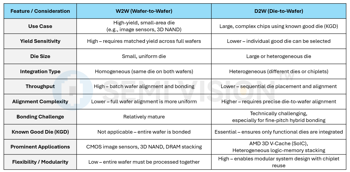
W2W: Ideal for high-yield, small-area die; offers alignment and throughput advantages. Common in image sensors and 3D NAND.
D2W: Suitable for large or complex chips usingknown good die (KGD)after wafer sort. Technically challenging but enables modular, heterogeneous integration.AMD’s 3D V-Cache (SoIC)is a prominent example using D2W hybrid bonding.

- Industry Applications and Leading Players

Hybrid bonding is currently deployed inCMOS image sensors,3D NAND, and emerginghigh-end logicchips.AMDwas the first to implement D2W hybrid bonding in commercial products. Leading equipment suppliers include:
BESI (Netherlands)
EVG (Austria)
Applied Materials (USA)
TEL – Tokyo Electron (Japan)
ASMPT (Singapore/HK)
SET (France)
SUSS MicroTec (Germany)
Shibaura Mechatronics (Japan)
These companies are aggressively developing hybrid bonding tools and ecosystems to support growing demand.
- Process Positioning and Future Outlook
The Future of Advanced Packaging: Decoding Besi’s Strategy in the AI Chip Stacking Era
As artificial intelligence and high-performance computing (HPC) drive semiconductor systems toward unprecedented levels of complexity and scale, back-end processes—once regarded as auxiliary—are now emerging as a critical frontier for innovation. At this pivotal moment,BE Semiconductor Industries N.V. (Besi), a leading packaging equipment provider based in the Netherlands, is positioning itself as a foundational enabler of the next generation of semiconductor manufacturing.
With deep investments inhybrid bonding,thermo-compression bonding (TCB),heterogeneous integration,co-packaged optics (CPO), andmobile chip stacking, Besi is not only delivering advanced tools but also shaping the strategic direction of the packaging ecosystem.
This article explores how Besi is evolving from a tooling provider into a central architect of the AI and chiplet-based packaging revolution. Drawing from insights in its investor presentations, we uncover not only the technical pillars but also Besi’s supply chain role, platform positioning, and competitive boundaries.
This article will cover the following key themes:
The evolution of AI chiplet package solutions: from 3D stacking and hybrid bonding to photonic integration and SoIC.
Performance advantages ofhybrid bondingover traditional micro-bump: bandwidth density, power efficiency, and cost-effectiveness.
Industrial adoption of hybrid bonding by major players likeIntelandBroadcom, including Foveros Direct and 3.5D XPU applications.
Technical analysis ofCPO (Co-Packaged Optics)and hybrid bonding convergence: case studies of TSMC COUPE and Broadcom/NVIDIA implementation.
Bonding process evolution fromHBM3 to HBM5and how Besi’s tools align with this transition.
Frontier technologies in mobile and smartphone chip stacking: from InFO-PoP to SoIC-X/P platforms.
Besi’s strategic roadmap and its growth potential in the AI-driven end market.
This content will not only help you understand how Besi is positioning itself in the rapidly evolving landscape of advanced chip packaging but also serve as a gateway to mastering the hybrid bonding ecosystem. If you’re curious about the commercial roadmaps, supply chain transitions, and long-term competitive outlook ofAI chip packaging,HBM,CPO, orSoIC, this article is your essential starting point.
For Paid Members, SemiVision will discuss topics on
Hybrid Bonding Supply Chain: A Global Overview
Advanced Packaging in the AI Era: BESI’s Strategic Bet on Hybrid Bonding
Hybrid Bonding at an Inflection Point
BESI at the Core of AI Packaging Transformation
Advanced Packaging in the AI Era: Global Capital Surge and BESI’s Central Role in the Supply Chain Transformation
TSMC Lead the Expansion of 2.5D/3D Packaging Capacity
Korea and the U.S. Target HBM and CPO Opportunities
Taiwan and China Fully Engaged; Europe Accelerating to Catch Up
Market Outlook: Advanced Packaging Becomes a Global Investment Focus
Rapid Growth in 2.5D/3D Packaging: BESI Accelerates High-Precision AI Assembly Solutions
Market Drivers: AI Workloads and Heterogeneous Integration
BESI’s Product Advantages: High Precision, High Contribution, High Growth
BESI Positions Itself at the Heart of AI Hardware Transformation
BESI Targets the Two Fastest-Growing Advanced Packaging Segments: Hybrid Bonding and Fluxless TCB
Fluxless Thermo-Compression Bonding: Emerging Use Cases with Strong Upside
BESI Expands Its Leadership in Die Attach and Advanced Die Placement for AI and Heterogeneous Integration
BESI’s Strategic Core: Centering on Advanced Packaging to Strengthen Its Leadership in Technology and Capital Allocation
BESI Accelerates R&D Investments to Power the Next Generation of Advanced Packaging Systems
Incidentally, a significant number of papers at recentIEEE ECTCandIEEE IITCconferences have focused onHybrid Bonding technologies. Professor Chen fromNYCU in Taiwanhas published research utilizingCu/Polymer Hybrid Bonding, whileITRIpresented a novelPolymer-Based Hybrid Bondingtechnique throughRDL interfacingat ECTC. Notably, Professor Chen has contributed numerous publications on 3DIC packaging in IEEE journals. In the future,SemiVisionwill be providing in-depth analysis on such innovative academic work.
BESI, in close collaboration withApplied Materials (AMAT), has also been actively engaged in Hybrid Bonding research. AtIEEE IITC, BESI and AMAT co-authored a paper specifically focused onDie-to-Wafer (D2W) Hybrid Bonding, highlighting the depth of their technical partnership in advancing next-generation packaging technologies.



Hybrid Bonding Supply Chain: A Global Overview
As a transformative technology breaking through the bottlenecks of interconnect density and power efficiency, hybrid bonding is quickly becoming a foundational layer in next-generation semiconductor packaging. Here is a detailed breakdown of key participants across the value chain:
- Equipment Vendors
Besi (BE Semiconductor Industries)
Offers fullWafer-to-Wafer (W2W)andDie-to-Wafer (D2W)hybrid bonding platforms.
Focuses on high-precision alignment and throughput scalability.
Integrated into SoIC, HBM, and logic stacking flows.
Active collaborations withTSMC, Intel, Samsung, andBroadcom.
EV Group (EVG)
A global leader in W2W hybrid bonding systems.
Supplies alignment + bonding tools for TSMC’s SoIC-L and Sony’s image sensor platforms.
Known for strength in optical and CIS applications.
Canon ANELVA
Specializes in copper planarization and interface cleaning.
Focuses on heterogeneous logic-memory stacking.
Deep collaboration with Japan-based IDMs.
SUSS MicroTec
Develops low-temperature bonding and thin-wafer handling modules.
Competitive in backside IC integration and precision microstacking.
- Foundries & Advanced Packaging Providers
TSMC
Full-scale deployment of SoIC-W (Wafer Level ), SoIC-X, SoIC-P hybrid bonding platforms.
CoWoS + SoIC is the core AI packaging architecture.
Partners includeApple, AMD, Broadcom, andNVIDIA.
Intel
Own hybrid bonding platformFoveros Direct, enabling 0 µm gap bonding.
Used in advanced nodes like Clearwater Forest and Meteor Lake.
Samsung
Pursuing hybrid bonding forHBM4/HBM5DRAM stacks.
Developing proprietary heterogeneous logic-memory integration flows.
- Materials and Service Providers
Shin-Etsu, JSR, DuPont
Supply bonding interface materials: adhesion layers, dielectrics, and insulation.
Enhance planarization, surface activation, and thermal conductivity.
ASE, Amkor, SPIL
Piloting D2W hybrid bonding lines.
Collaborating with Besi and EVG on qualification and process integration.
In the coming wave of advanced packaging, hybrid bonding is not just a technical innovation—it is a litmus test of platform integration, supply chain leadership, and capital scalability. Besi is no longer just a toolmaker; it is a central nervous system of the AI packaging revolution.
If you’re seeking to understand the full dynamics behind this technological shift—fromequipment,foundries, andmaterials, toreal-world applications—this article will equip you with the multidimensional insights necessary to navigate the next era of chip design and system integration.
Advanced Packaging in the AI Era: BESI’s Strategic Bet on Hybrid Bonding
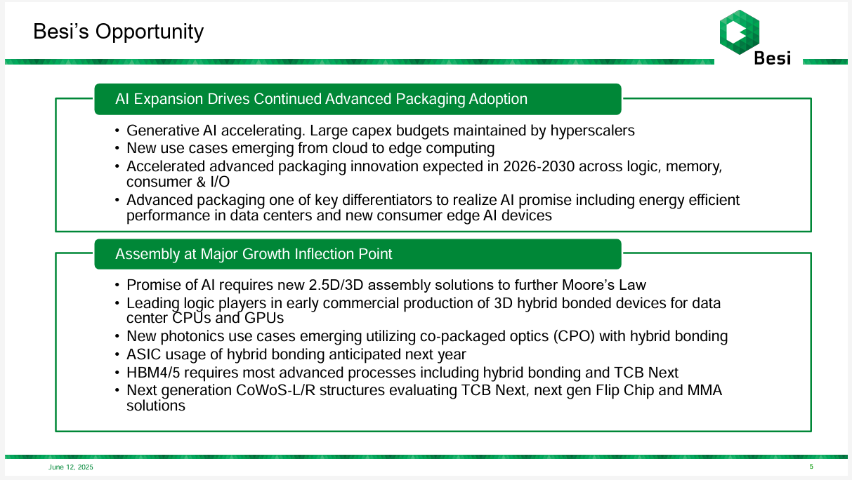
As generative AI rapidly evolves and demand for computing—ranging from cloud to edge—continues to surge, hyperscalers across the globe are pouring massive capital into expanding their high-performance computing (HPC) infrastructure.BE Semiconductor Industries (BESI)sees this AI infrastructure boom as a direct catalyst for the large-scale adoption of advanced packaging technologies, unlocking unprecedented growth opportunities for critical process innovations such ashybrid bonding.
AI Expansion Driving Advanced Packaging Innovation
The explosive growth of generative AI implies a steep rise in demand for logic chips, memory, and high-bandwidth I/O systems between2026 and 2030. To support these compute-intensive applications—from cloud data centers to consumer-grade edge AI devices—the industry requires high-performance, low-power, and highly integrated packaging solutions.
BESI highlights that advanced packaging will become a core enabler in realizing AI’s performance potential, acting as a key differentiator in improvingenergy efficiencyandcompute density. This demand is not limited to large cloud processors but will extend to edge devices such assmartphones,AR/VR headsets,AI-enabled cameras, andautomotive electronics, thereby expanding the total addressable market for advanced packaging and hybrid bonding.

2025年5月13日
Hybrid Bonding at an Inflection Point
BESI explicitly identifies hybrid bonding as a foundational technology in enabling new2.5D and 3D assembly architecturesneeded to sustain Moore’s Law. Major global logic chipmakers have entered the early stages of commercial production using3D hybrid bonding, aiming to boost integration between CPUs, GPUs, and memory in next-generation data center processors.
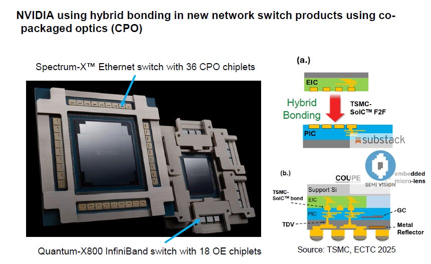
More notably,optical-electrical (OE) integrationis emerging as a new frontier for hybrid bonding, particularly inCo-Packaged Optics (CPO)platforms. CPO involves directly integrating optical transceivers with switch ASICs within the same package—a process that demandsultra-high interconnect densityandultra-low latency. Hybrid bonding is rapidly becoming the go-to solution for such high-frequency OE integration challenges.
BESI also emphasizes the critical role of hybrid bonding andTCB Next (next-gen thermo-compression bonding)in supportingHBM4/HBM5packaging, which requires extremely tight control oversignal integrity,thermal management, andstacking yield.
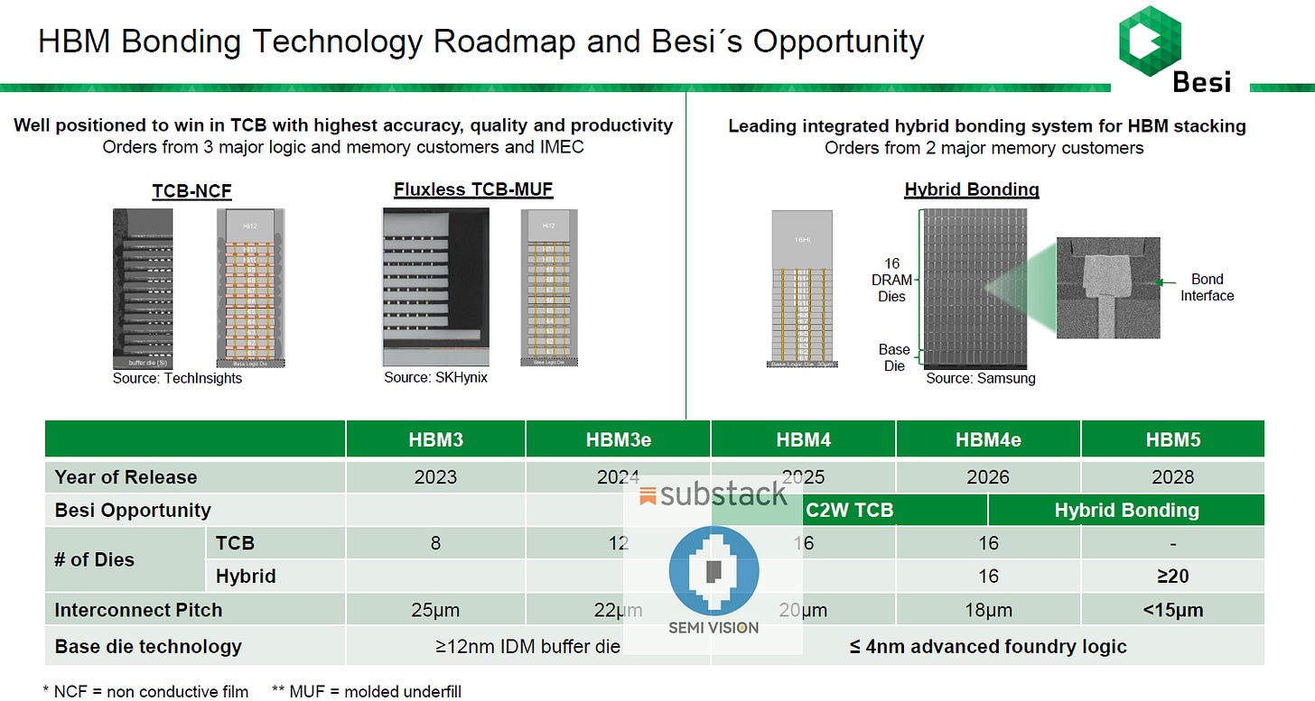
Platform Evolution and Strategic Roadmap
BESI continues to advance its technology platform to align with the evolving demands of next-generation packaging. Its product roadmap now includes support for a variety of key architectures such as:
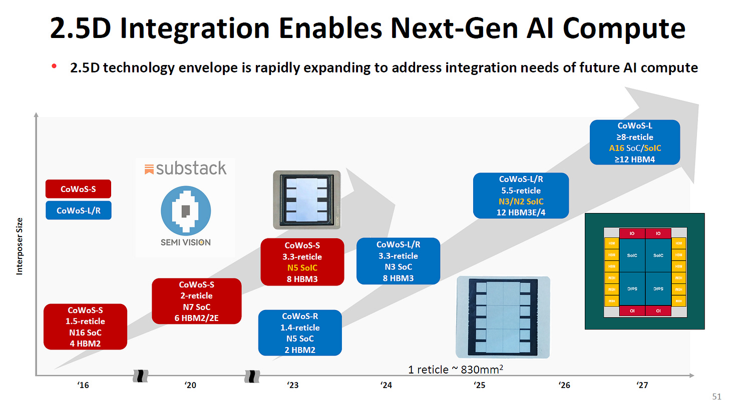
CoWoS-L (LSI )andCoWoS-R (RDL)
TCB Nextfor advanced thermo-compression bonding
Next-generation Flip Chip technologies
MMA (Multi Module Assembly)for complex heterogeneous integration
These solutions are designed not only for high-performance computing and AI chip stacking but also position BESI as acritical enablerof industry-wide packaging transformation. Through this, BESI is expanding its footprint across diverse application areas includinglogic, memory, and optical modules.
BESI at the Core of AI Packaging Transformation
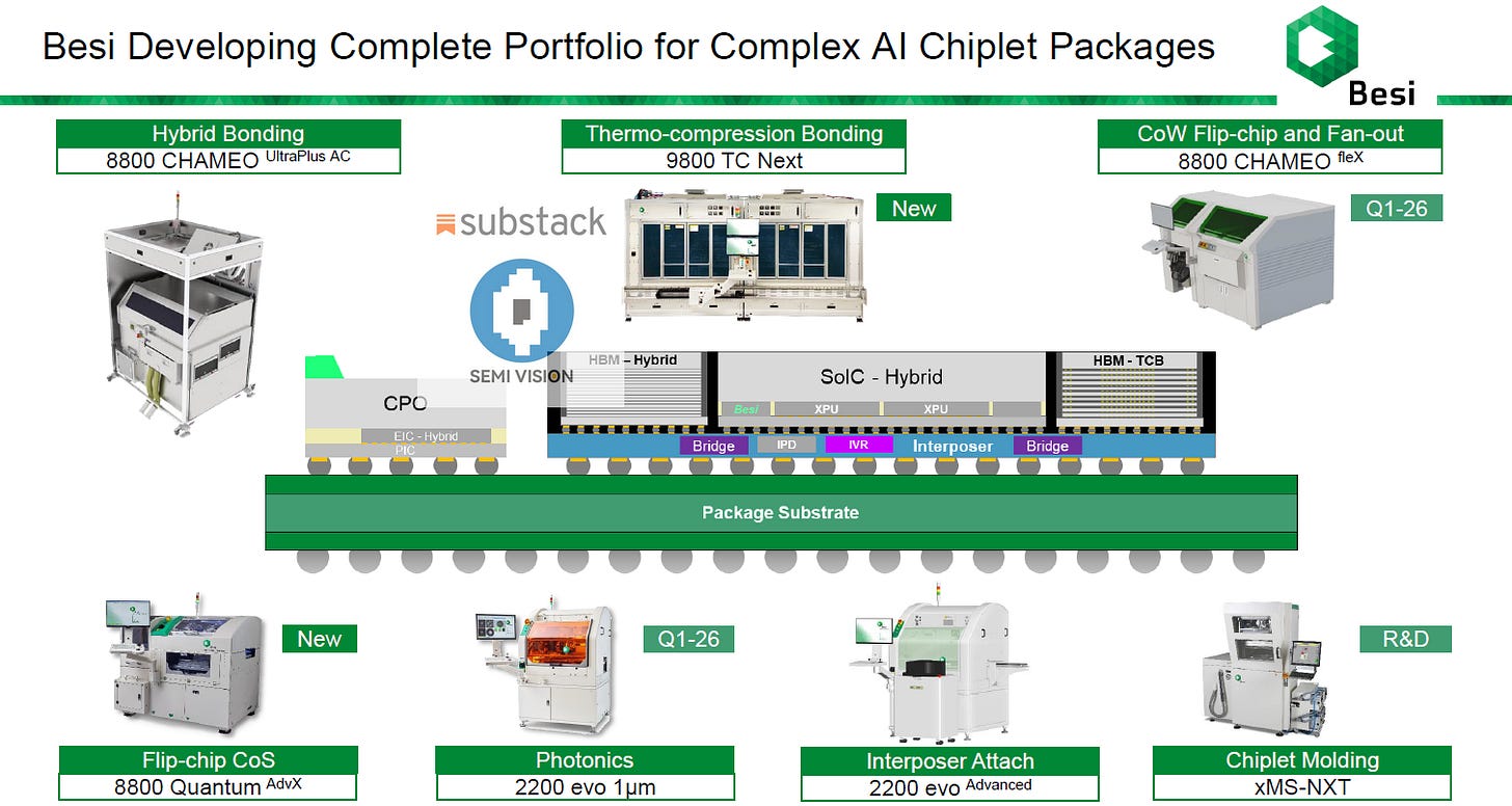
BESI is clearly positioning hybrid bonding as acentral engine of transformationfor advanced packaging in the AI era. Whether it’shigh-performance logic packagingin data centers,HBM memory stacking, or the realization ofCPO interconnects, BESI’s technologies are hitting a major inflection point for accelerated adoption.
As Moore’s Law faces increasing limitations in the coming decade,the convergence of hybrid bonding with system-level packagingis poised to unlock a new chapter of semiconductor innovation—and BESI stands at the forefront of this shift.
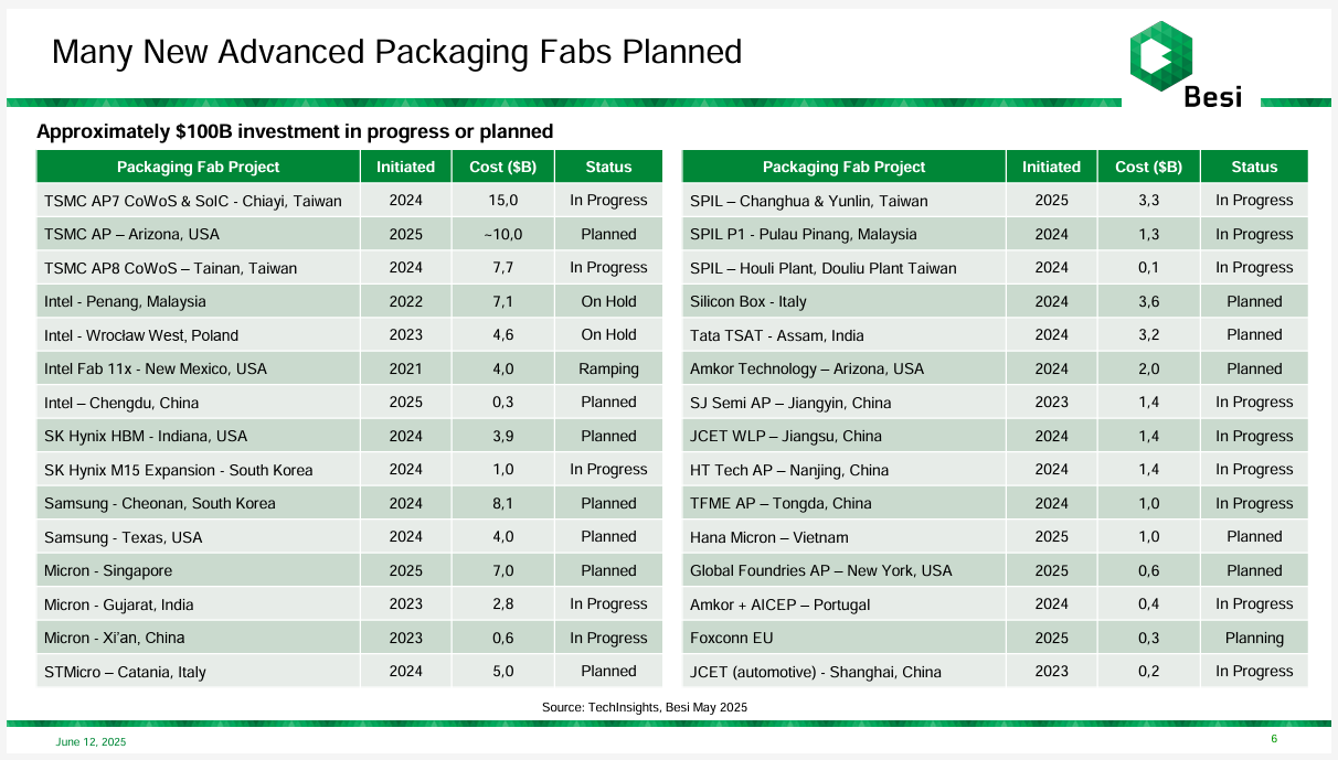
Advanced Packaging in the AI Era: Global Capital Surge and BESI’s Central Role in the Supply Chain Transformation
As artificial intelligence, high-performance computing (HPC), and memory stacking continue to reshape the semiconductor landscape,advanced packaging has emerged as a global battleground. According to data released byBESI in June 2025, more than$100 billion in capital expenditureis currently being planned or deployed for next-generation advanced packaging fabs worldwide. This wave of investment underscores the industry’s pivot—transforming packaging from a traditional “back-end” process into thecore of system-level integration. It also reveals the strategic moves by major foundries and OSATs to secure a lead in the AI era.
TSMC Lead the Expansion of 2.5D/3D Packaging Capacity
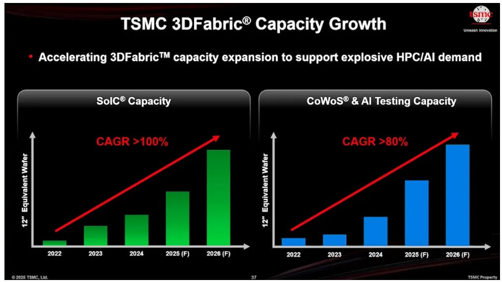

2025年5月17日
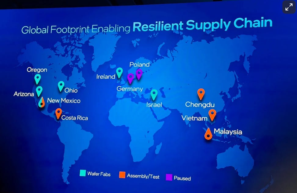
Intel, on the other hand, has adopted amulti-location strategyto diversify risks and resources. This includes sites in Penang, Malaysia (currently paused), Wroclaw, Poland (also paused), New Mexico’sFab 11x(ramping into production), and a new advanced packaging facility scheduled to begin inChengdu in 2025. These fabs are primarily aimed at assembling advanced logic chips using hybrid bonding and supporting large chip packages such asEMIBandFoveros Omni—critical for AI CPUs and GPUs.

2025年5月1日
Korea and the U.S. Target HBM and CPO Opportunities
Ashigh-bandwidth memory (HBM)andco-packaged optics (CPO)become central to AI architectures, Korean memory giantsSK HynixandSamsungare rapidly scaling up. SK Hynix is investing$3.9 billionin a new HBM packaging facility inIndiana, USA, and is also expanding production lines at itsM15 fabin Korea. Samsung, in parallel, is developing two massive packaging projects—$4 billion to $8.1 billion—inCheonan (Korea)andTexas (USA). These efforts will support HBM4, 3D stacking, and photonic integration.
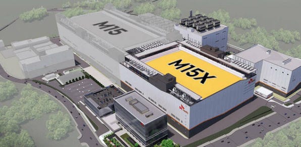
SK hynix Signs Investment Agreement of Advanced Chip Packaging with Indiana
In the U.S., companies likeMicron(with over $10 billion combined investments across Singapore, India, and Xi’an, China) andGlobalFoundries(New York) are enhancing their packaging capabilities to offerlow-latency, energy-efficient solutionstailored for edge AI and automotive applications.
Taiwan and China Fully Engaged; Europe Accelerating to Catch Up
Taiwanese OSAT leaders likeASEandSPILare doubling down on advanced packaging. SPIL is expanding inChanghua, Yunlin, and Taichung Houli, with a focus onflip chip, 2.5D/3D modules, and hybrid bonding. ASE is also pushing forward inPenang, Malaysia, partnering withBESIand other tool vendors to co-develop high-yield manufacturing solutions.


2025年6月18日
In China, companies such asTFME,Huatian,Tongfu Microelectronics (SJ Semi),JCET, andHT Techare building advanced packaging lines focusing onWLP,FOWLP, andco-packaged optical modules. These projects, launched primarily between 2023 and 2025, range from$100 million to $300 millionin investment.
InEurope,STMicroelectronicsandSilicon Boxinitiated expansion in 2024, with a$500 million fab in Catania, Italy, and a photonic packaging platform led by Silicon Box. New projects are also being planned inGermany and Portugal, signaling Europe’s intensified entry into next-generation packaging competition.
Market Outlook: Advanced Packaging Becomes a Global Investment Focus
According to BESI’s analysis, this packaging investment surge spans all major wafer manufacturing and OSAT ecosystems and is tightly coupled with the rise ofAI, HBM, CPO, heterogeneous integration, andedge computing. Foundries are vertically integrating packaging capabilities, while OSATs and materials/tool suppliers are simultaneously upgrading production lines—targetingClass 1 cleanroom standards,sub-micron alignment, andautomated high-throughput production.
AsMoore’s Law slows, advanced packaging is poised to take over as thenew engine of performance scaling. This global investment map reveals a collective embrace of the packaging transformation led by3D stacking and hybrid bonding, where BESI’s equipment solutions sit at the very heart of this industry-wide realignment.
Rapid Growth in 2.5D/3D Packaging: BESI Accelerates High-Precision AI Assembly Solutions
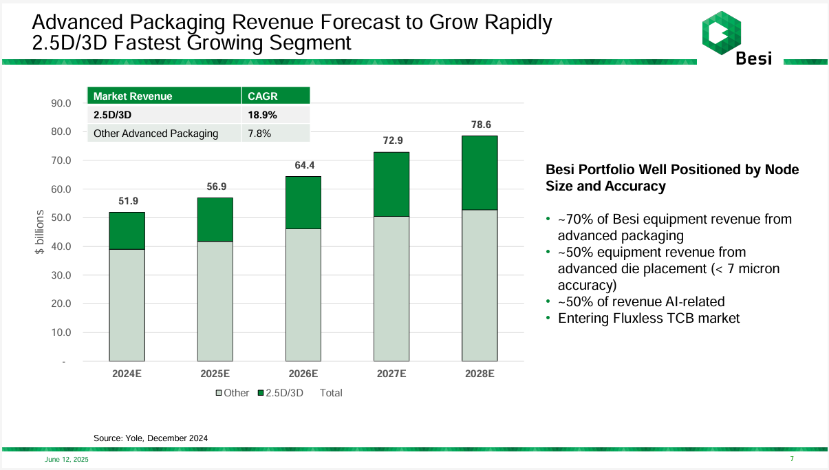
According to a December 2024 forecast fromYole Group, the globaladvanced packagingmarket is experiencing significant expansion—particularly within the2.5D and 3D packaging segments, which are projected to be the most explosive application categories over the next few years. The total market size is expected to grow from$51.9 billion in 2024to$78.6 billion by 2028, with 2.5D/3D packaging leading the pack at aCAGR of 18.9%, far surpassing the 7.8% CAGR of other advanced packaging technologies.
As a global leader insemiconductor assembly and bonding equipment,BE Semiconductor Industries (BESI)has strategically focused its product portfolio on this high-growth segment and has already secured a substantial market share and technological edge.
Market Drivers: AI Workloads and Heterogeneous Integration
With the rapid rise ofGenerative AI,high-performance computing (HPC),high-bandwidth memory (HBM), andmulti-chip modules (MCMs), there is increasing demand forhigh-density, low-latency, energy-efficient data movementbetween chips. Traditional packaging technologies are no longer adequate to meet the performance requirements of modern AI and computing systems.
2.5D packagingachieves high-speed interconnects through silicon interposers, while3D packagingtakes integration further byvertically stacking dies using hybrid bonding, offering ultra-short signal paths, improved bandwidth, and superior integration density.
These architectures are considered essential for futureAI chips,co-packaged optics (CPO)modules, andSoC-memory stacking. As such, mass adoption of these packaging methods is expected between2026 and 2028, fueling explosive growth in both equipment and materials markets.
BESI’s Product Advantages: High Precision, High Contribution, High Growth
According to BESI’s internal estimates,approximately 70% of its equipment revenue now originates from advanced packaging, reflecting a highly focused portfolio targeting high-value, high-barrier manufacturing processes.
Notably, around50% of BESI’s sales are attributed to high-precision die placement solutions, withalignment accuracy below 7 microns—a critical enabler for hybrid bonding and multilayer 3D stacking. As integration density continues to increase, BESI’s precision assembly capabilities will remain acore competitive differentiator.
Furthermore, abouthalf of BESI’s total business is directly linked to AI hardware applications, confirming not only a strategic market-product fit but also a strong alignment with long-term growth vectors. Particularly influxless Thermo-Compression Bonding (TCB), BESI is reinforcing its advantages incleanliness, yield, and reliability, which are vital for HBM, CPO, and SoIC modules that are highly sensitive to thermal and chemical variation.
BESI Positions Itself at the Heart of AI Hardware Transformation
From both a market structure and product strategy standpoint, BESI has successfully anticipated the explosive demand for2.5D/3D packagingand has positioned itself at the forefront of this transformation withhigh-precision, high-purity, and high-integration equipment platforms.
As the global semiconductor industry approaches a new era ofhigh-end 3D stacking around 2026, BESI’sadvanced die placement systems and hybrid bonding technologieswill become increasingly indispensable. In a time whereadvanced packaging, not just lithography, is driving Moore’s Law, BESI stands as a central enabler of the AI infrastructure revolution.
BESI Targets the Two Fastest-Growing Advanced Packaging Segments: Hybrid Bonding and Fluxless TCB
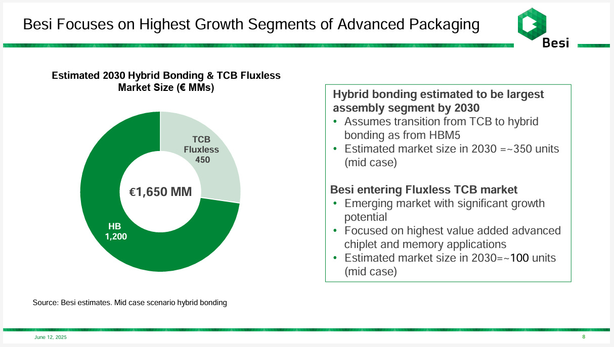
As the semiconductor industry enters a new era driven by AI and heterogeneous integration, advanced packaging is no longer simply about increasing I/O density or transmission efficiency. Instead, it has evolved into a foundational transformation of chip integration and system architecture. According to BESI’s latest market outlook,Hybrid Bonding (HB)andFluxless Thermo-Compression Bonding (Fluxless TCB)are projected to be the two fastest-growing assembly technologies in advanced packaging through2030, with a combined market size reaching€1.65 billion—€1.2 billion for HBand€450 million for Fluxless TCB.
Hybrid Bonding: The Largest Assembly Market in Advanced Packaging by 2030
BESI forecasts that, as demands for packaging precision and electrical performance intensify, applications such asHBM5, logic processors, and optical moduleswill transition from conventional TCB tohybrid bonding. This technology enablesdirect copper-to-copper and dielectric-to-dielectric bondingwith sub-micron interconnect pitch, making it essential for3D IC,SoIC,CoWoS-X, andCPOpackaging architectures.
Under BESI’s base-case scenario, thehybrid bonding equipment marketis expected to reach approximately€1.2 billion by 2030, with estimated shipments of around350 systems. This indicates that hybrid bonding is no longer a pilot or pre-production process—it is entering the mainstream era of volume manufacturing.
Fluxless Thermo-Compression Bonding: Emerging Use Cases with Strong Upside
In addition to hybrid bonding, BESI is also expanding its footprint in thefluxless TCBmarket. By eliminating the use of flux, this bonding technique offers superiorcleanliness, thermal performance, and long-term reliability. It is particularly well-suited forAI and HPC chips, where thermal dissipation and signal integrity are critical inchiplet integrationandHBM stacking.
While still in its emerging phase, BESI sees significant upside for fluxless TCB. By 2030, thefluxless TCB equipment marketis expected to reach€450 million, with an estimatedannual demand of 100 systems. Its value proposition is centered aroundhigh-value applications, includingHBM4/HBM5 memory stacksandmodular AI SoC + memory systems.
Strategic Positioning and Differentiation
BESI’s dual-pronged approach toHB and Fluxless TCBunderscores a clear strategy: focusing onprecision-centricandvalue-drivenapplications. As one of the few equipment providers capable of delivering bothsub-7μm die attachandhybrid bonding platforms, BESI occupies a critical position in the evolving packaging landscape.
From logic and memory stacking toco-packaged optics (CPO)andheterogeneous chiplet integration, BESI’s tools are enabling leading IDMs and OSATs to adopt next-generation packaging architectures. With major applications such asSoIC-X,HBM5, andCPOramping toward mass production, BESI has already secured a strong presence on the front lines of growth.
Enabling the Infrastructure of AI with Advanced Assembly Platforms
Through its focused investment inhybrid bondingandfluxless TCB, BESI is solidifying its leadership in the advanced packaging equipment market. As the global industry approaches a doubling in packaging value by 2030, these two technologies are not only performance enablers—they are foundational to the infrastructure of future AI computing.
By aligning with the highest-growth curves in packaging, BESI is executing a strategy that is bothtechnologically astuteandcommercially transformative, ensuring it remains a key player in the AI era of semiconductor innovation.

BESI Expands Its Leadership in Die Attach and Advanced Die Placement for AI and Heterogeneous Integration
According to data published byTechInsights in June 2025, BE Semiconductor Industries (BESI) is steadily increasing its global market share in bothdie attachandadvanced die placement, further solidifying its leadership position in the advanced semiconductor packaging equipment sector.
Die Attach Market Share Rises to 50% in 2024
Die attach is a critical process in semiconductor packaging, involving the precise placement and bonding of bare dies onto substrates or interposers. Between 2020 and 2024, BESI’s global market share in this segment increased from37% to 50%, underscoring both the company’s strong track record in reliable high-volume production and its sustained investment inautomation, high precision, and high-speed placement technologies.
As die sizes shrink and package architectures become increasingly complex, BESI has proven capable of addressing a wide range of assembly challenges, includingmulti-chip modules (MCMs), 2.5D/3D ICs, andheterogeneous integration systems. The company has become a go-to equipment provider for customers seeking best-in-class die attach performance.
Dominant Share in Advanced Die Placement Maintained at Over 80%
Advanced die placement refers to bonding technologies with sub-7μm placement accuracy, essential for next-generation packaging applications such ashybrid bonding, CoWoS, SoIC, CPO, and 3D stacking.
BESI has consistently led this segment, with global market shares of81%, 79%, 78%, and 81%from 2020 through 2023, and a new record of82% in 2024. This dominance highlights BESI’s deep technological moat in ultra-precision placement, enabling sub-micron accuracy and alignment at production scale.
This leadership is underpinned by continuous R&D investment. BESI’s integration ofhigh-speed vision alignment, dynamic compensation algorithms, andmechanically stabilized architecturesdelivers industry-leading accuracy, throughput, and defect control—especially critical forhigh-density chiplet modulesandhigh-bandwidth memory (HBM) stacks.
Strategic Outlook: Precision Packaging as the Backbone of AI and HPC
As AI and high-performance computing (HPC) drive the transition from monolithic logic chips tochiplet-based architectures, packaging has become a defining factor in overall system performance. BESI’s capabilities inhigh-accuracy placementandlarge-area module assemblyare perfectly aligned with this structural industry shift.
Its equipment is already widely deployed for key applications such asHBM packaging, heterogeneous SoC integration, andco-packaged optics (CPO)—critical enablers of the next wave of AI and edge computing systems.
BESI’s growing market share reflects not only top-line expansion but also growing trust fromtier-one chipmakers, includingTSMC, AMD, Intel, andSamsung. As the industry pushes toward smaller nodes, higher integration, and lower power, BESI’s precision platforms are becoming indispensable to achieving those goals.
BESI as the Foundation for the Next Generation of Advanced Packaging
BESI has firmly established itself as the industry leader in bothdie attachandadvanced die placement. As the world moves towardexplosive demand for 2.5D/3D ICs, hybrid bonding, and AI-optimized packaging, BESI’s technology edge in precision assembly will serve as a cornerstone for its long-term growth and influence in the semiconductor supply chain.

BESI’s Strategic Core: Centering on Advanced Packaging to Strengthen Its Leadership in Technology and Capital Allocation
In its 2025 strategic presentation,BE Semiconductor Industries (BESI)clearly articulated its long-term growth vision and value creation agenda. As a global leader in semiconductor assembly and bonding equipment, BESI attributes its consistent success to a disciplined strategy centered around advanced packaging, underscored by a focused execution framework and medium-to-long-term operational roadmaps.
Seven Strategic Pillars: Balancing Technology, Scale, Sustainability, and Capital Return
Maintain Best-in-Class Technology Leadership
BESI aims to solidify its leadership in key process segments such as die attach, hybrid bonding, and thermocompression bonding, ensuring it remains the top choice for AI, high-performance computing (HPC), and memory stacking applications.
Expand Presence in Wafer-Level Assembly (WLA)
As packaging trends move toward wafer-level integration, BESI plans to accelerate its deployment of WLCSP, fan-out, and chiplet-to-wafer platforms, broadening its addressable solutions portfolio.
Increase Market Reach Across Diverse Applications
BESI seeks to penetrate emerging markets including edge AI, automotive, and high-frequency radar by enhancing go-to-market strategies and expanding its customer base.
Enhance Scalability and Reduce Structural Costs
Through modular design, automation, and flexible manufacturing, BESI targets reduced cost-per-unit and lead time, while improving adaptability across varying production environments.
Exceed Sustainability Targets for 2026 and 2030
The company is committed to optimizing energy efficiency, lowering carbon emissions, and greening its supply chain—particularly in the design of energy-efficient and material-efficient assembly systems.
Pursue Strategic Acquisitions of Complementary Technologies
BESI will accelerate its entry into adjacent domains such as photonics integration, D2W hybrid bonding, and nanomaterial processing via targeted M&A initiatives to enhance cross-platform capabilities.
Return Value to Shareholders via Capital Allocation Policy
Through sustained dividends and share buybacks, BESI remains committed to shareholder returns while focusing capital investments on high-growth, high-return segments.
Six Execution Principles: Systematic Governance from R&D to Market Expansion
BESI’s strategy is anchored in the following disciplined principles:
Maintain R&D Leadership
Ensure innovation velocity and control of core technologies exceed that of competitors.
Focus on High-Growth Advanced Packaging Applications
Prioritize investments in the fastest-growing and highest-value packaging segments.
Partner with Industry Leaders (“Win with the Winners”)
Establish deep, long-term partnerships with top-tier IDMs, foundries, OSATs, and AI disruptors.
Prioritize Profitability Over Market Share
Target high-margin applications, avoiding volume-driven or low-price competition.
Deliver Cutting-Edge Systems with Mainstream Cost and Lead Time
Provide leading performance at accessible cost and deployment timelines, ensuring scalability and manufacturability.
Maintain Flexible and Scalable Manufacturing Models
Support customer evolution and demand shifts through agile capacity and modular architectures.
Grow in a Sustainable Manner
Build long-term competitive advantage across technology, financial, environmental, and social dimensions.
Strategic Precision in a Decade of AI-Driven Semiconductor Transformation
BESI’s strategy is both consistent and forward-looking. Rather than pursuing scale for its own sake, the company is laser-focused onadvanced packaging as the structural growth engineof the semiconductor industry. Throughtechnological leadership, flexible manufacturing, sustainability integration, and precision capital deployment, BESI positions itself as a resilient and high-growth enabler of next-generation AI and heterogeneous compute systems.
In an era defined by chiplet disaggregation and architectural reinvention,BESI has secured a central role in the core assembly technologies that will shape the AI decade ahead.
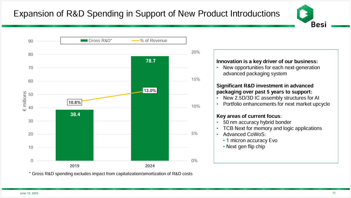
BESI Accelerates R&D Investments to Power the Next Generation of Advanced Packaging Systems
Research and developmentremains the cornerstone of innovation in semiconductor assembly technologies. According to BESI’s latest strategic briefing, the company has significantly increased its R&D expenditures over the past five years, with a sharp focus onAI-driven 2.5D/3D IC architectures,hybrid bonding, andthe evolution of CoWoS platforms.
Doubling Down on R&D: Increased Investment and Strategic Focus
In 2019, BESI’s R&D spending totaled€38.4 million, accounting for10.8%of its annual revenue. By 2024, this figure had grown to€78.7 million, now comprising13.0%of revenue. This upward trajectory reflects a deliberate capital shift towardsdeep technology development and product innovation, ensuring BESI maintains its leadership in high-value, high-growth advanced packaging segments.
This growth is not merely quantitative. It reflects BESI’s strategic acceleration in converting R&D intocommercially viable next-generation assembly solutions, perfectly timed to capitalize on the industry’s inflection toward 3D system architectures and heterogeneous integration.
R&D Innovation as the Driver of the Next Product Wave
BESI defines its R&D mission ascreating new entry points in each packaging system generation. The next five years are expected to be a pivotal phase formass adoption of 2.5D and 3D IC packaging, foundational to enablingAI chip modularization, high-bandwidth memory stacking, andCPO (Co-Packaged Optics)integration.
With sustained investment, BESI is proactively positioning its portfolio forthe next major product cycle, extending its systems to address moregranular, specialized, and differentiated use cases.
Four Key Pillars of BESI’s Current R&D Focus
50nm-Class Hybrid Bonder Development
In response to rising demand for ultra-fine pitch hybrid bonding, BESI is developing bonding platforms with50-nanometer alignment precision. These will supportnext-generation 3D IC stacksandoptical module integrationwith tighter interconnect spacing and higher data bandwidth.
TCB Next: The Next-Generation Thermocompression Bonding Platform
Aimed at memory and logic chip assembly, TCB Next enhancesthermal stability,fluxless bonding, andcleanroom-grade process control—ideal forHBM4/5,DDR6, and other high-end memory integrations.
Advanced CoWoS Assembly Platform
To address the complexity ofmulti-layer interposers and chiplet-based architectures, BESI is developing a new CoWoS-compatible assembly line, featuring itsnext-gen Evo systemwith1-micron placement accuracy, enabling high-yield large-die and multi-die modules.
Next-Gen Flip Chip Processing Equipment
In anticipation ofCXLandPCIe Gen6/7adoption, BESI’s new Flip Chip platform delivershigher throughput,lower thermal stress, andoptimized solder joint control, enhancing its competitiveness in both standard and customwafer-level packagingmarkets.


PreviousNext
TopLatestDiscussions








See all