Next-Gen AI Cooling: Moving Toward Microchannel-Based Architectures
Next-Gen AI Cooling: Moving Toward Microchannel-Based Architectures
- Source: SemiVision
- Author: SEMIVISION
- Published: 2025-07-09T23:10:59+08:00
- URL: https://tspasemiconductor.substack.com/p/next-gen-ai-cooling-moving-toward Next-Gen AI Cooling: Moving Toward Microchannel-Based Architectures


Next-Gen AI Cooling: Moving Toward Microchannel-Based Architectures
Original Articles By SemiVision Research (IEEE ECTC , KLA , EVGroup , Meta , TSMC ,HP , Google , ASE , SEMI , Henkel)

Jul 09, 2025
∙ Paid

At the 2024 IEEE ECTC conference, a highly notable technical paper titled“Moving Towards Microchannel-Based Chip Cooling”was presented. This paper is of exceptional value not only for its technical depth, but also because of the prestigious affiliations of its authors, who come from leading global organizations such asSEMI, KLA, EVG, Meta, TSMC, HP, Google, and ASE.

TSMC
TSMC showcased their“Si‑Integrated Micro‑Cooler”at IEEE ECTC 2024, presenting wafer‑level microchannels etched directly into the backside of active chips using MEMS/DRIE. These channels are integrated with CoWoS packaging and interposers to support heat fluxes up to2.6 kWwhile maintaining ΔT ≈ 63 °C . Ongoing work includes trench, pillar, and planar microchannel variants, with pillar-based structures showing the best performance.

EVG (EV Group)
EVG provides the core wafer-bonding technology required for embedding microchannels at wafer scale. TheirGEMINIandEVG501systems support high-force, large-area bonding (up to 350 kN), essential for integrating microchannel wafers between SoC and HBM . Their presence at ECTC 2024 highlights their leadership in wafer-level bonding for heterogeneous integration .

KLA (SPTS Technologies)
Through SPTS, KLA supplies advanced MEMS process tools critical for microchannel fabrication. Their DRIE systems — based on the Bosch process — are regarded as industry leaders for achieving high-aspect-ratio features (like deep trenches and TSVs) . These tools are vital for producing reliable microchannel structures in silicon.

https://www.kla.com/products/chip-manufacturing/etch
HP’s long-standing expertise inMEMS-based printhead manufacturing(with thousands of microfluidic nozzles per chip) shows deep experience in large-scale backside etching and fluidic control surfaces . Although not actively marketing chip cooling solutions, their MEMS heritage suggests they could adapt their microfluidic technologies for thermal management applications.
Meta, Google, ASE
While specific microchannel initiatives by Meta or Google are not public, both companies are active collaborators in ECTC and advanced packaging R&D. ASE (Amkor/ASE Group) — a major OSAT player — is positioned forsystem-level integration, including wafer-to-wafer bonding, interposer assembly, and final packaging necessary to implement microchannel systems .
Purpose and Industry Significance
The core objective of this study is to address the thermal bottlenecks facing next-generation AI chips and to propose feasible, scalable solutions for the future. As AI models expand into the trillion-parameter era, the power density of a single SoC has exceeded the capabilities of traditional thermal modules. Air cooling and single-point liquid cooling are no longer sufficient, especially in the context of 3D-stacked advanced packaging. To tackle this challenge, the team proposes a novel architecture centered aroundwafer-level microchannel cooling.
Key Technologies and Ecosystem Participation
The paper outlines several key technological innovations and highlights the involvement of an extensive supply chain to support manufacturable solutions, including:
Wafer-on-Wafer (WoW) Bonding: SoC and HBM wafers are bonded at the wafer level, with a MEMS-based microchannel wafer inserted in between. This bonding is supported byEVG (EV Group), a leading provider of wafer bonding solutions.
MEMS-Based Microchannel Fabrication: To create fluidic channels within silicon wafers, deep reactive ion etching (DRIE) processes are applied. Key equipment and metrology providers includeSPTS Technologies(now part of KLA) andKLAitself.
System-Level Package Integration: The architecture integrates SoC, HBM, and a microchannel wafer into a single stack, mounted on an interposer to form a full system-in-package. Foundries and OSATs such asTSMCandASEplay critical roles in backend processing and advanced thermal packaging.
TSMC’s Strategic Participation: From TIM Challenges to No-TIM Innovation
Traditional structure:AI Chip → TIM1 → Lid → TIM2 → Cold Plate
TIM1 (between die and lid) and TIM2 (between lid and cooling module) significantly influence total thermal resistance.
Voids, poor adhesion, and non-uniform contact in TIM layers often degrade thermal performance.
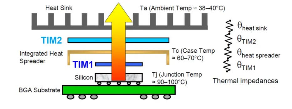
To address this,TSMC’s contribution to the paper includes a forward-looking proposal of a “No-TIM” architecture, which eliminates the TIM layer entirely. Instead, it introducesdirect thermal contact between the chip backside and the cooling structure, significantly reducing interface thermal resistance. This concept aligns with other papers TSMC has presented at ECTC, emphasizing its strategic investment in thermal co-design at the package level.



2025年7月3日
Closing Thoughts and Technical Outlook
This paper is an outstanding example of international, cross-disciplinary collaboration across the semiconductor ecosystem. It illustrates that future semiconductor innovation will not be defined solely by signal integrity or packaging density, but also bythermal architecture and co-design.
In tomorrow’s AI computing era, the question is no longer just“how many chips can you stack?”, but rather,“how well can you dissipate the heat from those high-performance chips?”This is whereSoW architectures, microchannel integration, No-TIM strategies, and embedded liquid coolingwill define the next competitive frontier.


The core challenge in AI chip thermal management today lies squarely within the chip itself. Therefore, it is crucial for foundries to propose systematic solutions from their end of the value chain. The following details further elaborate on this point, with a focus on TSMC’s efforts under silicon-based architectures—specifically in the exploration of microchannel cooling, DRIE/MEMS applications, copper pillar array design, TIM material challenges, and No-TIM architectures. These thermal solutions are applicable not only to SoW and CoWoS but also to silicon photonics-integrated advanced packaging.

2025年6月13日

2025年6月2日

2025年6月27日
As artificial intelligence computing enters the era of trillion-parameter models—with training power consumption reaching hundreds of kilowatts—the design bottleneck for AI chips is shifting from compute capacity and memory walls to another invisible barrier: thethermal wall. Today’s mainstream cooling technologies, including air and traditional liquid cooling, are increasingly inadequate in handling heat flux densities exceeding 300 W/cm². Moreover, the uneven thermal distribution across AI chips introduces additional complexity to thermal management. Conventional heat dissipation structures, such as “AI Chip → TIM1 → Lid → TIM2 → Cold Plate,” introduce multiple thermal interfaces that significantly increase thermal resistance, limiting both heat transfer efficiency and overall system performance.
In response to this thermal crisis, the industry is now shifting its focus upstream:thermal path design should be initiated at the advanced packaging and wafer manufacturing stages, rather than being treated as a passive challenge at the backend. This article stands at that inflection point—examining innovations in wafer-level integration, MEMS fabrication, and microchannel-based liquid cooling systems, with a particular focus on how TSMC and other leading foundries are spearheading system-level thermal breakthroughs.
The article opens by highlighting the promise of wafer-level microchannel structures—such as those fabricated using DRIE (Deep Reactive Ion Etching) techniques to create silicon through-holes or channel features. These channels enable liquid coolant to be introduced directly adjacent to heat sources, dramatically shortening the heat transfer path. Such a design not only supports advanced packaging techniques like CoWoS and 3DIC, but also allows for localized cooling at hotspots, reduces overall thermal resistance, and mitigates thermal fluctuations, enabling high-efficiency on-chip convective cooling. TSMC’s pillar-based microchannel design, for instance, demonstrates the ability to handle thermal loads of up to 2.6 kW, while keeping temperature differentials within 63 °C.
Additionally, the article explores a transformative shift in wafer-level thermal design: theNo-TIM architecture. Unlike traditional TIM materials, which are prone to void formation, adhesion issues, and thermal aging, the No-TIM approach integrates cooling channels directly into the backside of the silicon chip. This allows coolant to directly interface with the heat-generating regions, eliminating intermediate materials and their associated thermal resistance and reliability risks—thereby opening a new thermal pathway for future high-power AI chips.
The article also addresses the mechanical reliability concerns arising from high heat flux and materials mismatch. It explores strategies such as structural optimization (e.g., Cu pillar arrays, low-pressure-loss channel designs) and system-level thermal simulation, aimed at ensuring long-term stability under extreme operating conditions.
Ultimately, this article is not just about technological advancement—it reflects a fundamental shift in design philosophy:foundries are no longer just manufacturers, but integral architects of thermal management for AI chips. As we enter the era of 3D ICs, Chiplets, and System-on-Wafer architectures, only by embedding thermal optimization at the silicon level can we truly overcome the limits of heat.
This is a revolution at the intersection of packaging, silicon process engineering, and liquid cooling innovation. It is a philosophical evolution from “cooling” to “thermal co-design”—and it marks a critical leap forward in enabling the future of AI.


While wafer-level liquid cooling and No-TIM architectures are gaining traction as revolutionary solutions,Thermal Interface Materials (TIMs) remain an indispensable partof today’s thermal management strategies—especially given the realities of chip packaging, manufacturability, and system integration. Among TIM providers,Henkel has emerged as a key player, advancing both material performance and process integration for high-power AI chip packaging.
As AI chips evolve towardhigh-density, high-power, and multi-die stackingconfigurations—such as Chiplet + HBM + 3D integration—thermal management has become a central concern in packaging design. Within this architecture, TIMs serve a critical function: transferring heat from chips or stacked modules to heat sinks, cold plates, or liquid cooling systems with minimal thermal resistance.
Henkel, a global leader in adhesives and materials solutions, has developed acomprehensive and modular ecosystemfor TIMs under its well-known brands such asBergquistandLoctite. Henkel’s TIM portfolio spans six major categories: gap fillers, gap pads, SIL pads, thermal adhesives,phase change materials (PCM), and thermal greases. These materials are widely deployed across high-end processors, 5G base stations, data centers, automotive electronics, and industrial control systems.
On the technology front, Henkel continuously pushes the performance boundaries of TIMs. A prime example is itsnext-generation Bergquist Hi Flow THF 5000UTphase change material, which remains solid at room temperature and melts upon heating. This material achieves avery low thermal resistance of 0.04°C·cm²/Wandthermal conductivity over 8.5 W/m·Kwith bondline pressures under 10 psi—making it particularly suitable forfragile, high-performance AI chipswhere ultra-thin and low-pressure TIM1 layers are critical.
ForTIM2 interfaces, which span from chip lid to cold plate, Henkel offers a variety of gap pad solutions designed to accommodate mechanical compliance and absorb thermal stress. TheTGP 10000ULMpad, with a thermal conductivity ofup to 10 W/m·K, supports high-power modules, especially in data center and automotive environments. The product line includes ultra-soft, UL-certified, and electrically conductive options to address varying thickness and compliance needs.
Beyond raw material performance, Henkel places strong emphasis onprocess-friendly and automation-compatible designs. The THF series PCMs can bepre-applied to lids or cold plates, avoiding issues like manual grease application, air gaps, and inconsistent contact. Gap fillers can bedispensed, printed, or transfer-appliedusing dual-component systems to meet the high-precision requirements of advanced packaging facilities.
Henkel’s TIM development aligns with the most critical trends in AI/HPC packaging, including:
High-conductivity phase change materials for ultra-thin TIM1 applications.
Soft and conformal gap pads/fillers for TIM2 heat spreading.
Interface materials compatible with microchannel liquid cooling structures.
Multifunctional TIMs for next-generation architectures such as Co-Packaged Optics (CPO) and System-on-Wafer (SoW).
In summary, Henkel is playing an increasingly strategic role in AI thermal solutions throughmaterial innovation, low-pressure bonding design, automation readiness, and high-power system compatibility. As chip power density continues to climb, Henkel’s TIM technologies are poised to remain a foundational element in future AI packaging thermal designs.



2025年5月27日
For Paid Members , SemiVision will discuss topics on
Foundry Perspective: Why Chip Thermal Architecture Must Be Led by the Foundry Side
MEMS Architecture may be a good choice in liquid cooling system
Microchannel Liquid Cooling Concept drive next ai chip generation
MEMS/DRIE Process and Silicon Stress Management
What is DRIE (Bosch Process)?
Copper Pillar Array for Enhanced Thermal Convection Paths
TIM Material Research vs. No-TIM Architecture Innovation
System-Level Co-Optimization: Foundry-Led Direction for Future Thermal Packaging
AI Era Heat Flux Challenge: Hotspots Entering Overheating Zone
TSMC’s Perspective: Silicon Cooling Die and Chip-Level Thermal Solutions
What Is Thermal Budget?
Why Is Thermal Budget Important?
Understanding Thermal Budget: A Critical Constraint in Chip and System Design
System-Level Power Considerations
Challenges to Thermal Budget and Microchannel Limitations
Recent Breakthroughs: Advanced Solutions to Push the Thermal Budget Further
Advancing Toward Microchannel-Based Chip Cooling: A Thermal Revolution for the AI Era
Microchannel Geometry and Packaging Challenges
Foundry Perspective: Why Chip Thermal Architecture Must Be Led by the Foundry Side
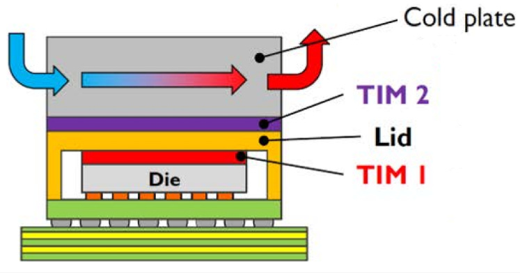
Source: Xidian University, Xi’an
The classical AI chip thermal stack typically follows this structure:
AI Chip → TIM1 → Lid → TIM2 → Cold Plate.
Within this heat dissipation path, multiple interface layers and material-related imperfections—such as voids or poor adhesion—contribute to increased thermal resistance, ultimately limiting the chip’s thermal budget and overall performance.
From the foundry's vantage point, the early stages of wafer fabrication and packaging provide a unique opportunity to define and control the heat flow path at the chip level. By initiating the design of the thermal architecture at the source, the foundry can not only improve thermal efficiency but also prevent integration challenges that may arise in later stages of advanced packaging.
This upstream integration enables:
Optimized Heat Spreading Paths:Direct engineering of silicon and interposer layers (e.g., using microchannels or embedded heat spreaders).
Material System Co-Optimization:Early-stage selection and integration of TIM materials or No-TIM alternatives that align with silicon process constraints.
Advanced 3D/heterogeneous compatibility:Ensuring that the thermal strategy scales effectively with 2.5D, 3DIC, and chiplet architectures, where vertical and lateral heat dissipation become even more critical.
As AI chips push toward higher power densities and tighter thermal margins, it is no longer viable to treat thermal design as a post-fabrication packaging problem. A foundry-led, co-optimized thermal strategy is now a prerequisite for high-performance and reliable AI silicon.
MEMS Architecture may be a good choice in liquid cooling system
In advanced packaging for thermal management, the structure involves bonding a SoC wafer with an HBM wafer at the wafer level, and integrating a microchannel wafer into the stack. This entire assembly is then mounted onto an interposer to form a system-level package. This highly integrated architecture inherently enables the development of tightly coupled cooling structures directly at the wafer level, serving as a compelling example of how foundries can take an active role in thermal management from the earliest stages of packaging design.
Microchannel Liquid Cooling Concept drive next ai chip generation
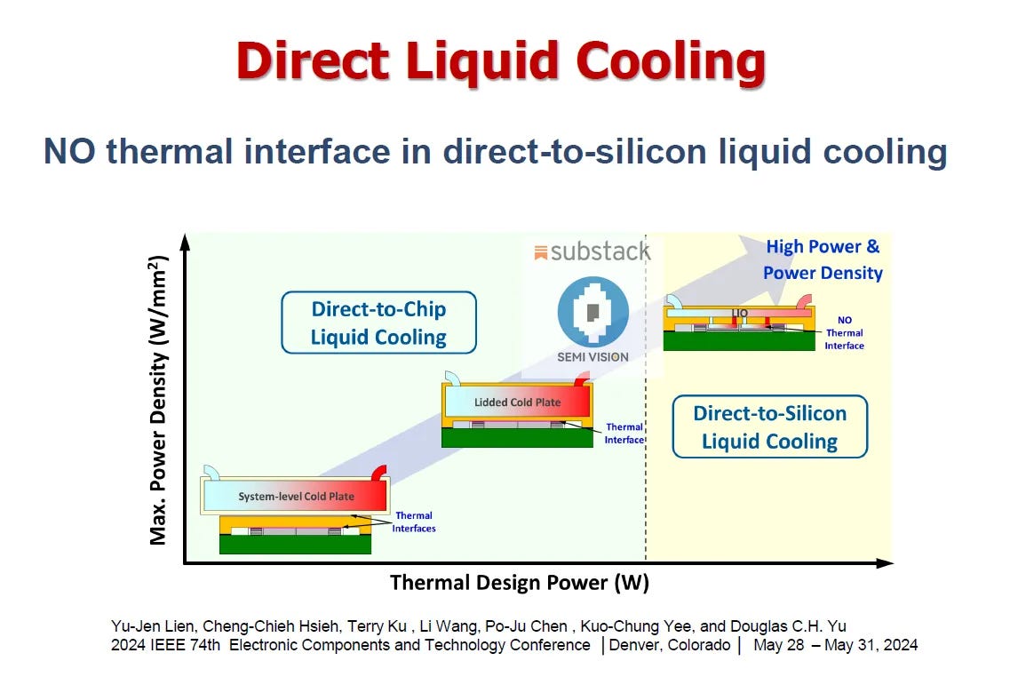
In its IEEE ECTC papers and follow-up discussions, TSMC introduced the concept ofDirect Water Cooling (DWC)by etching microchannels directly into the backside of active dies using MEMS/DRIE processes. These microchannels are then integrated with CoWoS packaging and the interposer to form a unified cooling path. The cooling solution is capable of handling heat fluxes up to2.6 kW, with temperature differentials controlled within approximately63 °C.
TSMC explored various microchannel structures, includingtrench,pillar array, andplanar channeldesigns, with thepillar-based microchannelconfiguration demonstrating the best thermal performance.
2025年7月3日
MEMS/DRIE Process and Silicon Stress Management
Microchannels are fabricated at the wafer level using DRIE (Deep Reactive Ion Etching) to create TSVs or trench structures—commonly applied to silicon-based wafers. This process enables highly precise, high-aspect-ratio etching and is suitable for batch fabrication, making it ideal for microfluidic and thermal management applications in advanced packaging.
However, DRIE introduces mechanical challenges such as vertex stress (excessive stress at corners), wafer warpage, and increased risk of cracking or breakage during subsequent processing.
To mitigate these risks, foundries must implement stress relief structures and carefully manage trench pitch and aspect ratios, ensuring that the silicon microchannel structures remain stable and reliable under extreme thermal conditions and repeated liquid cooling cycles.
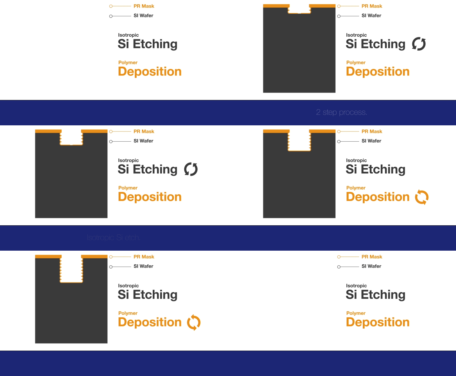
What is DRIE (Bosch Process)?
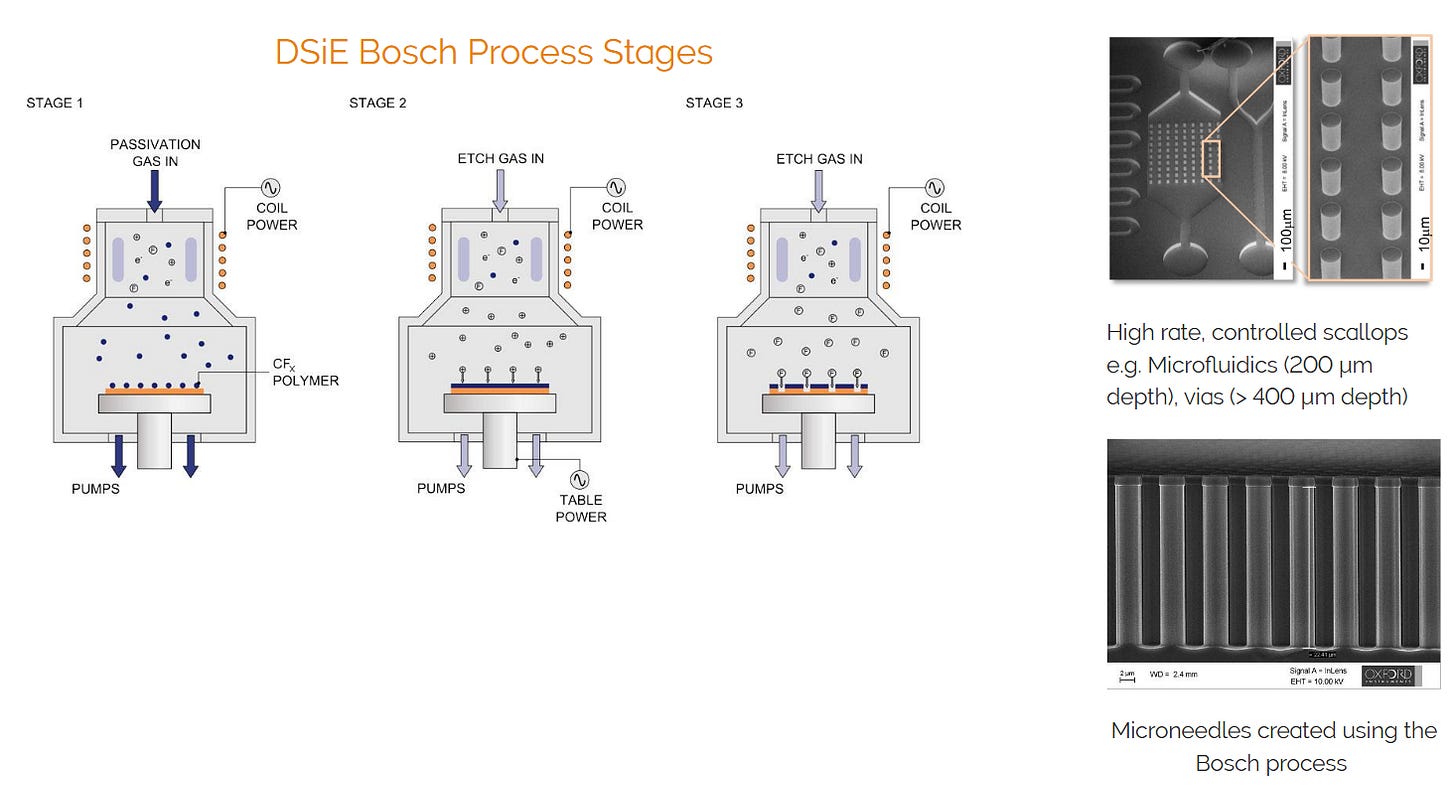
DRIE is a microfabrication technique used to etch deep and narrow features into silicon wafers with high precision. It is a key process in MEMS (Micro-Electro-Mechanical Systems) manufacturing and is particularly suited for creating microchannels, vias, and cavities with vertical sidewalls. The process alternates between etching and passivation steps to achieve high aspect ratios while maintaining structural integrity.
Copper Pillar Array for Enhanced Thermal Convection Paths
In addition to microchannels, TSMC has introduced theCopper Pillar Arrayas a supplementary structure to strengthen thermal convection pathways. These copper pillars can serve asmicro-bumpsorthermal columns, conducting heat directly from the active silicon layer and providing an additional solid-state thermal transfer path.
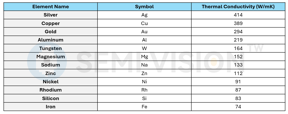
Copper, with its significantly higher thermal conductivity compared to TIM powders or phase-change interface materials, helpsreduce local thermal resistance. When tightly integrated with the cooling fluid pathways, the copper pillar array significantly enhancessystem-level thermal dissipation efficiency.

TIM Material Research vs. No-TIM Architecture Innovation
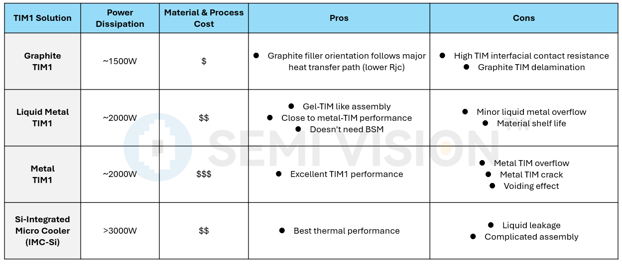
TIM Material Challenges: Voids, Adhesion, and Reliability
Common issues with TIM1/TIM2 layers include:
Interface Voids: These reduce thermal connectivity and increase thermal resistance.
Poor Adhesion: Leads to delamination between layers.
Material Degradation: High temperatures can cause material failure andpump-out, where TIM is displaced over time.
Indium alloy TIMs (≈80 W/m·K) offer excellent thermal conductivity but require surface metallization (e.g., Ti/Au or Ni/Au) on the chip backside and lid, along with areflow processto ensure low interfacial thermal resistance and high reliability.

No-TIM Architecture: A Breakthrough Innovation
TSMC has explored aDirect Water Cooling (DWC)architecture that eliminates the need for intermediate TIM layers. In this approach, microfluidic cooling channels are etched directly into the silicon die, enablingdirect contactbetween the cooling fluid and the heat-generating active layer. This significantly reduces interfacial thermal resistance.
In comparative tests across three architectures:
Pure DWC Architecture: Achieved2.6 kW heat loadwith aΔT of 63 °C— the best performance.
Oxide (OX) TIM Architecture: Reached2.3 kW / 83 °C.
Liquid Metal TIM Architecture: Handled around1.8 kW / 75 °C.
Among different microchannel structures, thepillar-based microchannelconfiguration demonstrated the most effective thermal performance.

System-Level Co-Optimization: Foundry-Led Direction for Future Thermal Packaging
Foundries now play a leading role in designingchip-level microfluidic cooling architectures, including aspects such as channel geometry, pillar layout, fluid inlet placement, and bonding interfaces. This ensures seamless integration with downstream CoWoS or SoIC system-level packaging.
TSMC’sCoWoS-S platformcombineshigh-thermal-conductivity RDLswith optimized TIM structures at the packaging level. It also exploresSi-lid microchanneldesigns, aiming to achieve a fully integrated packaging solution with low thermal resistance and high heat dissipation.
On thereliabilityfront, TSMC has also studied the electromigration performance ofCu/SnandCu/Ni/Sn/Cumicro-bump structures under high current density. These efforts are crucial to ensuring long-term stability of microchannel structures and thermal pillar attachments under prolonged high-temperature cycling.
Leading foundries likeTSMCare no longer passive responders in thermal design, butkey architects in AI chip thermal management. Thermal strategies are now embedded from thewafer fabrication stage, rather than being retrofitted in back-end packaging.
TSMC is actively exploring multiple thermal innovations:
Microchannel liquid cooling
Copper Pillar thermal columns
High-performance TIM materials
No-TIM architectures
Looking ahead, foundries must work closely with chip designers, packaging engineers, and system thermal architects toco-optimize chip-level heat transfer pathways, enabling AI modules to sustain extreme power densities in the era of3D ICs, chiplets, and System-on-Wafer (SoW)architectures.
The Thermal Wall Challenge of AI Chips: From Microchannel Liquid Cooling to TSMC's Chip-Level Thermal Management Technologies
As generative AI models scale beyond trillions of parameters and each training cycle consumes hundreds of kilowatt-hours of energy, the bottleneck of the AI era is no longer just compute or memory—it is heat. AI chips are confronting an invisible barrier known as theThermal Wall,which not only constrains chip performance and reliability but also pushes the limits of packaging and system-level design.

AI Era Heat Flux Challenge: Hotspots Entering Overheating Zone
According to the Intel–Purdue research presented at IEEE ECTC 2024 in“Moving Towards Microchannel‑based Chip Cooling”, modern AI chips now exhibit heat flux densities exceeding300 W/cm², with some hotspots reaching600 W/cm². Traditional cooling methods such as air and standard liquid cooling struggle to manage such intense, non-uniform heat sources effectively
Key Limitations of Traditional Cooling
Inadequate for high-density heat flux over 300 W/cm²
Poor handling of non-uniform hotspots
Leads to performance throttling and reliability issues
Proposed Solution: Silicon-Based Microchannel Cooling
Proximity to source: Embeds microchannel structures within silicon or packaging layers, minimizing thermal resistance
High convective efficiency: Microscale channels achieve elevated heat transfer coefficients
Hotspot-targeted cooling: Enables localized liquid cooling tailored to chip thermal maps
High integration potential: Compatible with 3D‑IC, chiplets, and HBM packaging formats

Practical challenges include fluid distribution uniformity, packaging stress management, and addressing CTE mismatches between materials
TSMC’s Perspective: Silicon Cooling Die and Chip-Level Thermal Solutions
“TSMC’s Direct-to-Silicon Liquid Cooling: Background and Technical Evolution.”
This solution integrates active cooling functionality directly into the chip packaging structure, with several key highlights:
Stacking a Cooling Die with the Logic Chip
A microfluidic-structured silicon die is directly stacked on top of the logic die, forming a localized liquid-cooling pathway within the package.
Co-Integration of Silicon Channels with the RDL
The cooling die is co-packaged with the Redistribution Layer (RDL). A low-temperature bonding process ensures mechanical integrity and reliable heat dissipation performance.
High-Flow, Low-Pressure Drop Channel Design
The microchannel design minimizes bends and flow obstructions, achieving significantly lower pressure drops compared to traditional cold plate systems.
Wide-Area Temperature Uniformity and Hotspot Compensation
Experiments demonstrate that the cooling die can reduce AI accelerator hotspot temperatures by over 20°C, improving overall frequency stability and power efficiency.
This approach reflectsTSMC’s system-level thinking, where thermal management is no longer seen as the responsibility of a single mechanical component. Instead, it becomes anintegral part of advanced system-in-package solutions, forming aclosed-loop thermal architecturealongside3D IC stacking, heterogeneous integration, CoWoS, and SoIC-Xtechnologies.
Heat Meets Packaging: The New Era of Integrated Thermal Design
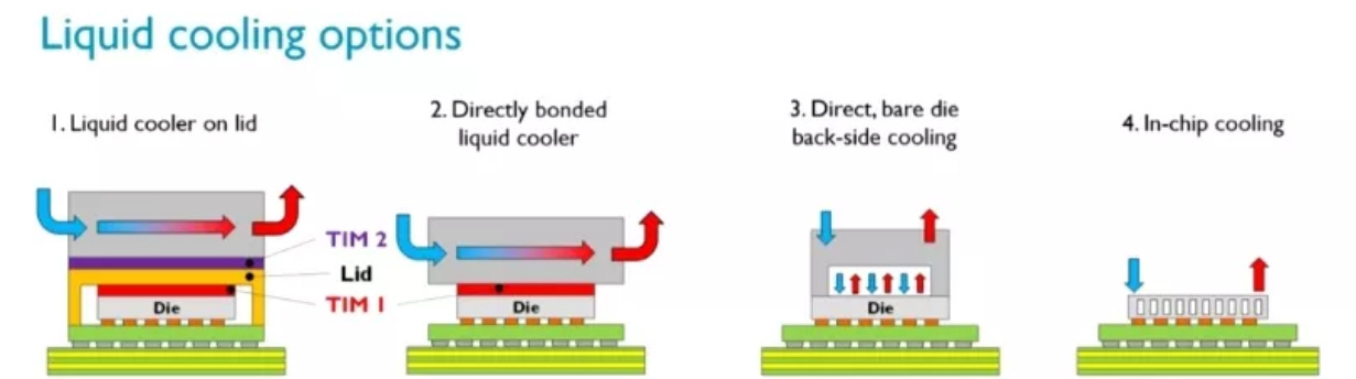
From Intel–Purdue’s in-chip microchannel cooling to TSMC’s silicon cooling die architecture, the industry clearly recognizes: “the next front in packaging is thermal management.”
Thermal-Aware Co-Design
Thermal modeling is now woven into early design stages—alongside power integrity (PI), signal integrity (SI), and mechanical stress. Thermal-aware co-design ensures heat pathways are actively managed rather than retrofitted.
Redefining Packaging Responsibilities
Chips are no longer merely compute engines. Packaging modules must now deliver power, interconnects, cooling, and mechanical strength. As illustrated in microchannel, silicon-lid, and cooling die designs, packaging has expanded its functional scope.
System-Level Thermal Intelligence
Future packaging will likely embed thermal control algorithms—like Thermal AI Controllers—with sensors, hotspot scheduling, and fluidic control integrated directly into the chip-level cooling solution.
Shaping the AI Compute Landscape
From microchannel liquid cooling →
To embedded cooling dies →
Silicon heat exchangers →
Optimized heterogeneous thermal paths
These technologies will underpin next-decade high-performance computing—from 3D ICs to SoW strategies. The real AI thermal frontier lies not within the chip, but in whoever can first break through the Thermal Wall with advanced packaging design.
Thermal management is now a matter of packaging innovation, system-level integration, and chip-level intelligence — ushering in a comprehensive era of heat-aware design that supports extreme power-density AI modules.
What Is Thermal Budget?
In semiconductor and electronic system design, theThermal Budgetrefers to thetemperature difference between the maximum allowable junction temperature (T,max) of the chip and the maximum ambient temperature (Tambient,max) in which the product operates.

Tmax: The highest temperature the semiconductor die (junction) can safely operate at (e.g., 125°C or 150°C).
Tambient,max: The maximum expected temperature of the surrounding environment (e.g., 85°C for outdoor applications).
Why Is Thermal Budget Important?
The thermal budget determines whether a system can effectively dissipate heat under harsh temperature conditions. If the chip overheats, it may throttle performance, degrade over time, or even fail permanently.
Understanding Thermal Budget: A Critical Constraint in Chip and System Design
The Thermal Budget typically refers to the maximum heat dissipation capability a chip can tolerate, encompassing the maximum allowable junction temperature (Tmax), thermal resistance, and the cooling requirements determined by the chip’s power consumption. Its significance is reflected in several key areas:
Performance and Reliability
Excessively high junction temperatures can lead to:
Clock frequency throttling
Increased error rates
Physical degradation or failure of the die
These factors ultimately shorten the lifespan and reduce the reliability of the chip.
Packaging Design Constraints
Thermal budget is consumed by various packaging-related components:
Thermal Interface Materials (TIM)
Package structure and thickness
For instance, the thermal resistance of the TIM bonding layer alone can consume 30–40% of the total thermal budget, leaving limited margin for the rest of the thermal path.
System-Level Power Considerations
High-density AI chips often exhibit Thermal Design Power (TDP) values exceeding hundreds to thousands of watts. This creates an immense demand for thermal headroom to prevent overheating and avoid hitting the thermal wall—a bottleneck that limits further performance scaling.
The thermal budget is not merely a physical metric—it's a fundamental design constraint that connects chip performance, packaging architecture, and system-level cooling. Effectively managing this budget is essential for enabling next-generation AI and high-performance computing systems.
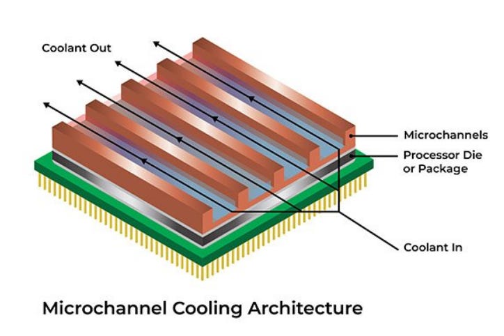
Key Advantages of Microchannel Cooling for Thermal Budget Enhancement
Significantly Reduced Thermal Resistance
By embedding cooling channels within the chip or packaging layers, the heat conduction path is drastically shortened. Compared to traditional cold plates, this results in a substantial drop in thermal resistance.
High Heat Flux Handling Capability
Microchannel systems can sustain heat flux densities of300 W/cm² or more, while maintaining thejunction temperature within safe operational limits.
Controlled Flow & Optimized Pressure Drop
Channel geometry and manifold design allow both single-phase and two-phase cooling to achievelow-pressure drops, aligning with packaging power constraints and mechanical thickness limits.
Overall, microchannel coolingexpands the effective thermal budgetby reducing internal temperature rise and thermal jitter, ensuring greater system thermal reliability.
Challenges to Thermal Budget and Microchannel Limitations
Despite its advantages, microchannel cooling faces several limitations:
Uneven Fluid Distribution and Hotspot Management
In parallel microchannel configurations, improper manifold designs (e.g., U/I/Z-type) can lead to non-uniform flow and inadequate cooling in localized hotspots. Incorporating nanofluids may improve thermal uniformity, but adds complexity to fluid management systems.
Packaging Integration and Structural Reliability
Combining cooling channels with chip packaging must consider CTE mismatch, mechanical stress, and packaging strain. The thermal interface between TIM channels, silicon, and metal layers also consumes part of the thermal budget—sometimes more than 30%.
Complexity of Two-Phase Cooling
While two-phase cooling (boiling) provides excellent heat transfer efficiency, it introduces design complexity. Engineers must manage boiling pressure, condensation recovery, and avoid dry-out (loss of coolant contact).
Recent Breakthroughs: Advanced Solutions to Push the Thermal Budget Further
Two-Phase Embedded Cooling
A research team at the University of Tokyo (2025) developed a two-phase embedded cooling system with up to 7× the efficiency of traditional designs. It achieves a COP (Coefficient of Performance) of 100,000 and handles over 1 kW/cm² heat flux, significantly improving the chip’s thermal budget. Another preprint study reported a Critical Heat Flux (CHF) of 1,682 W/cm² on SiC chips, with a COP of 23,615, demonstrating high cooling efficiency with minimal pressure drop.
Through-Chip Microchannels
The latest research features through-silicon microchannel arrays capable of handling power densities beyond 10⁴ W/cm², while maintaining temperature rise below 60 K. This vertical design allows coolant to directly access multiple heat layers, drastically enhancing thermal budget capabilities.
Embedded Nanofluid Smart Cooling
By integrating nanofluids with optimized manifold structures, targeted cooling for hotspot regions becomes feasible. This improves localized cooling efficiency and helps extend the system’s overall thermal budget control.
Microchannel cooling—especially with embedded, two-phase, or nanofluid-enhanced systems—is redefining the boundaries of thermal design. As AI chips scale toward extreme power densities, mastering the thermal budget is no longer optional—it’s a core engineering frontier.
Beginning with the microchannel cooling technologies introduced by Intel and Purdue, it is evident that such approaches substantially enhance the thermal budget of AI chips. However, with packaging power levels continuously rising—reflected in ever-increasing TDP values and heat flux densities—there is an urgent need forhigher-efficiency and more reliable thermal solutionsgoing forward.
Technologies showing great promise for expanding the thermal budget include:
Two-phase embedded microfluidics, which offer massive improvements in heat removal efficiency;
Through-silicon microchannel designs, which drastically shorten the heat conduction path;
Intelligent nanofluid control, which helps mitigate uneven hotspot cooling;
Andco-design of packaging, involving the joint optimization of TIM, RDL, and cooling architecture to fully maximize the thermal budget.
Advancing Toward Microchannel-Based Chip Cooling: A Thermal Revolution for the AI Era
As artificial intelligence and high-performance computing (HPC) evolve rapidly, chip power density and packaging complexity have escalated to the point whereconventional cooling methods are reaching their limits. When surface-level heat flux exceeds300 W/cm², solutions like air cooling and traditional cold plates are no longer sufficient. In response, the industry is turning toward more efficient, localized thermal management strategies—among whichmicrochannel-based liquid coolinghas emerged as a leading next-generation solution.
Why Microchannel Cooling?
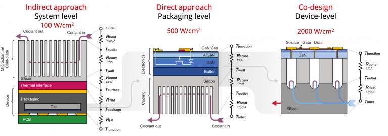
Conventional cooling technologies such as heat sinks, heat pipes, and cold plates are mature and widely adopted in desktops and servers. However, in high-power AI chips such as NVIDIA’s B100, Cerebras’ WSE, or AMD’s MI300,non-uniform hotspotscan lead to thermal throttling, performance degradation, or even physical failure. Microchannel cooling offers several critical advantages:
Proximity to the heat source: Microchannels can be integrated directly into the chip surface or inter-die layers in 3D stacks, minimizing thermal resistance.
High convective heat transfer coefficient: Microscale channels promote the transition from laminar to turbulent flow, significantly boosting thermal performance.
Modular design: Channel geometry and distribution can be customized to align with hotspot locations.
Adaptability to high heat flux: Both single-phase and two-phase liquid cooling methods allow microchannels to support several hundred W/cm² of heat flux.
Single-Phase vs. Two-Phase Microchannel Cooling
The research comparessingle-phase cooling(e.g., water or glycol-based coolants) withtwo-phase cooling(e.g., refrigerant boiling). Two-phase systems leverage latent heat from liquid–vapor transitions, providing much higher heat removal without requiring a proportional increase in flow rate or pressure. This makes them ideal for ultra-high-power applications, although they bring increased design complexity—including pressure regulation, condensation loops, and dry-out prevention.
Microchannel Geometry and Packaging Challenges
The geometry (rectangular, circular, serrated) and dimensions (width, depth, spacing) of microchannels impact the thermal resistance, pressure drop, and flow uniformity. Key packaging challenges include:
Managing thermal interfaces between silicon and metal cooling structures
Balancing pressure drop and ensuring fluid distribution uniformity
Designing interfaces compatible with advanced packaging (e.g., 2.5D/3D IC, HBM)
Ensuring material reliability and mitigating packaging-induced mechanical stress
The paper highlights the value of thin, high-thermal-conductivity silicon layers, paired with low-resistance TIMs and integrated joints, to improve overall cooling module feasibility within packaging constraints.
Experimental Validation and Performance Results
Thermal and fluidic performance data from various microchannel configurations showed that:
Microchannel cooling can effectivelymaintain chip hotspot temperatures below 70°C
Achievedthermal resistance under 0.1 K·cm²/W, outperforming conventional cooling by several times
Increasing channel count reduces per-channel pressure drop, though at the cost of increased flow partitioning and packaging complexity

Future Development and System-Level Integration
The study explores future applications of microchannel cooling in 3D ICs, advanced packaging, and in-chip fluidic channels. As AI chips evolve from planar to vertically stacked and heterogeneously integrated architectures, cooling technologies must evolve in tandem with chip design to address the thermal challenges of megawatt-scale computing modules.
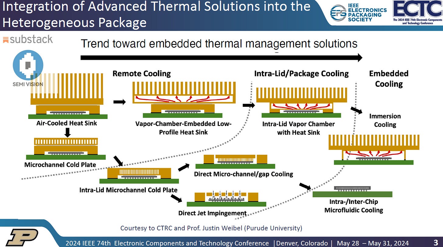
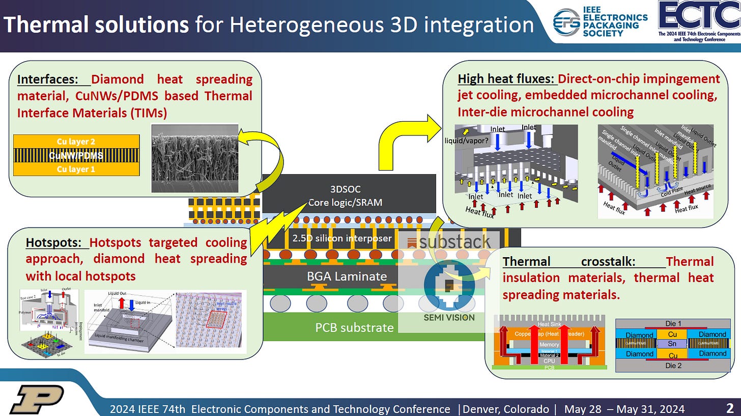
Microchannel cooling is no longer just a topic of academic research—it is becoming a core enabler of next-generation AI packaging. By combining advances in materials science, fluid mechanics, and semiconductor packaging, this technology is rapidly transitioning into industrial adoption, offering a revolutionary leap in cooling capacity for the infrastructure powering AI computation.


PreviousNext
TopLatestDiscussions








See all