From Custom SRAM to Optical SerDes: How Marvell Builds the Data Highways for AI Chips
From Custom SRAM to Optical SerDes: How Marvell Builds the Data Highways for AI Chips
- Source: SemiVision
- Author: SEMIVISION
- Published: 2025-07-09T15:04:48+08:00
- URL: https://tspasemiconductor.substack.com/p/from-custom-sram-to-optical-serdes From Custom SRAM to Optical SerDes: How Marvell Builds the Data Highways for AI Chips


From Custom SRAM to Optical SerDes: How Marvell Builds the Data Highways for AI Chips
Original Articles By SemiVision Research (Marvell , TSMC , AWS ,Microsoft ,Nvidia, Broadcom)

Jul 09, 2025
∙ Paid
Marvell Leads AI Chip Infrastructure Innovation: A Full-Stack Transformation from Custom XPU to Optical Interconnects
With the explosive growth of generative AI, large language models (LLMs), and bandwidth-intensive inference workloads, global data centers are undergoing a profound transformation driven by fundamental technology shifts. From processor architecture and memory access to interconnect interfaces and advanced packaging, the boundaries of traditional chip design are being redefined. In this context, Marvell positions itself at the core of this revolution with a “full-stack custom platform” approach, integrating design IP, advanced process nodes, packaging, and high-speed interconnects (SerDes / Optical I/O), becoming a powerful enabler of next-generation AI infrastructure.
Surge in AI Infrastructure Capital Expenditure
According to market data cited by Marvell, capital expenditures from the top four U.S. cloud service providers—Amazon, Microsoft, Google, and Meta—for AI infrastructure have been growing at a 46% compound annual growth rate since 2023, projected to reach $327 billion by 2025. This investment wave signifies a clear shift from general-purpose CPU-centric compute toward accelerated architectures centered on GPUs, TPUs, and XPUs—now becoming the new standard in modern data centers.
At the same time, emerging players such as OpenAI and xAI (model-first), Tesla and Apple (application-first), and Sovereign AI pioneers like Humain and Stargate are rapidly developing custom ASICs and memory systems, contributing to a diversified, decentralized, and co-optimized AI infrastructure ecosystem.
Breaking the GPU Monopoly with Custom XPU Architectures
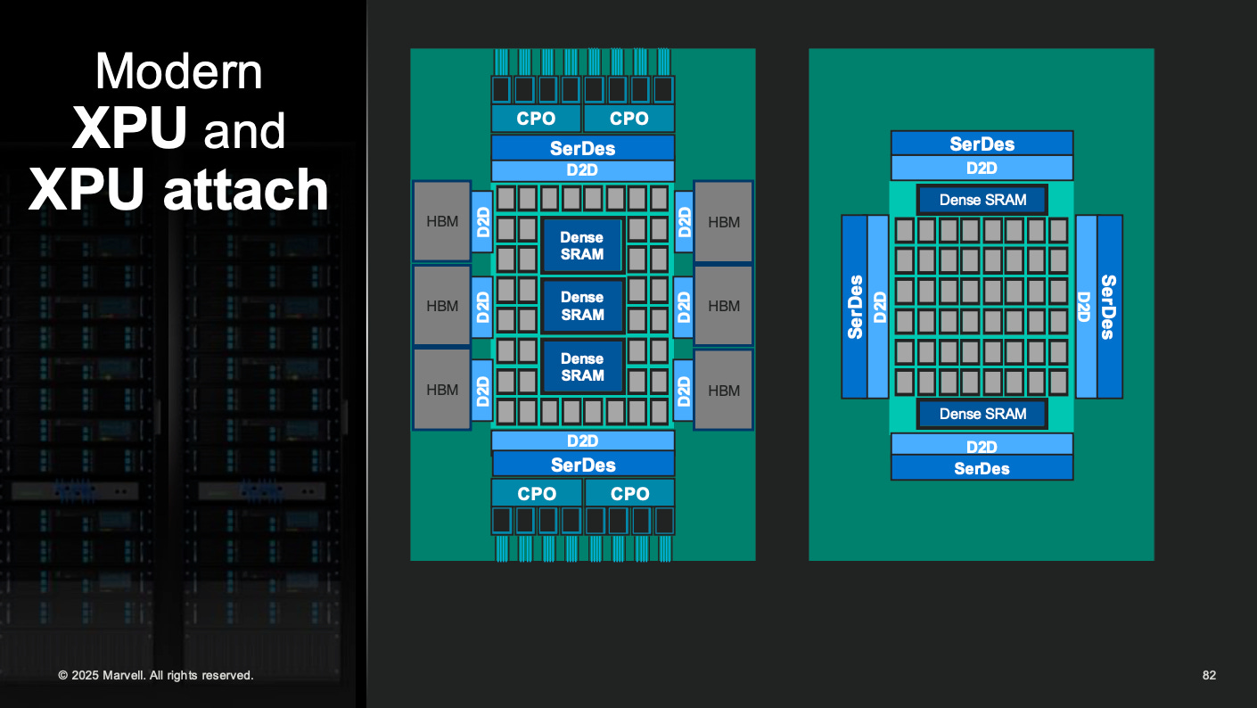
Amid rising chip design and supply chain costs—especially as NVIDIA GPUs remain expensive and scarce—many cloud providers are moving toward in-house ASIC designs to improve performance-per-watt and manage total cost of ownership (TCO). Marvell’s “XPU + XPU Attach” architecture defines two major custom chip domains:
Custom XPU: Tailored compute cores for AI inference, signal processing, or general-purpose compute tasks.
Custom XPU Attach: Supporting components including SerDes, D2D, scale-up fabric, memory pooling controllers, security, and management engines.
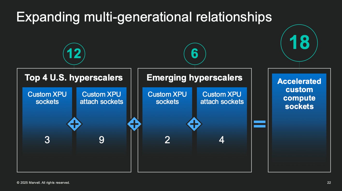
This architecture allows Marvell to provide complete core-to-interconnect solutions, offering flexible, customer-specific chip designs. To date, Marvell has deployed 12 sockets (3 XPUs and 9 Attach chips) among the top four cloud providers and 6 additional sockets among emerging hyperscalers, totaling 18 AI acceleration chips in production—evidence of its platform strategy’s broad industry validation.
Full-Stack Technical Superiority: From Silicon to System
Marvell’s strongest competitive edge lies in its ability to integrate from silicon to system across five core pillars:
System Architecture: Assists customers in defining data flow and parallel compute models for optimized SoC architectures.
Design IP: Offers high-performance SerDes, SRAM, memory controllers, and interconnect IPs.
Silicon Services: Supports cutting-edge process nodes (e.g., 2nm, 14Å, 16Å) with advanced logic design capabilities.
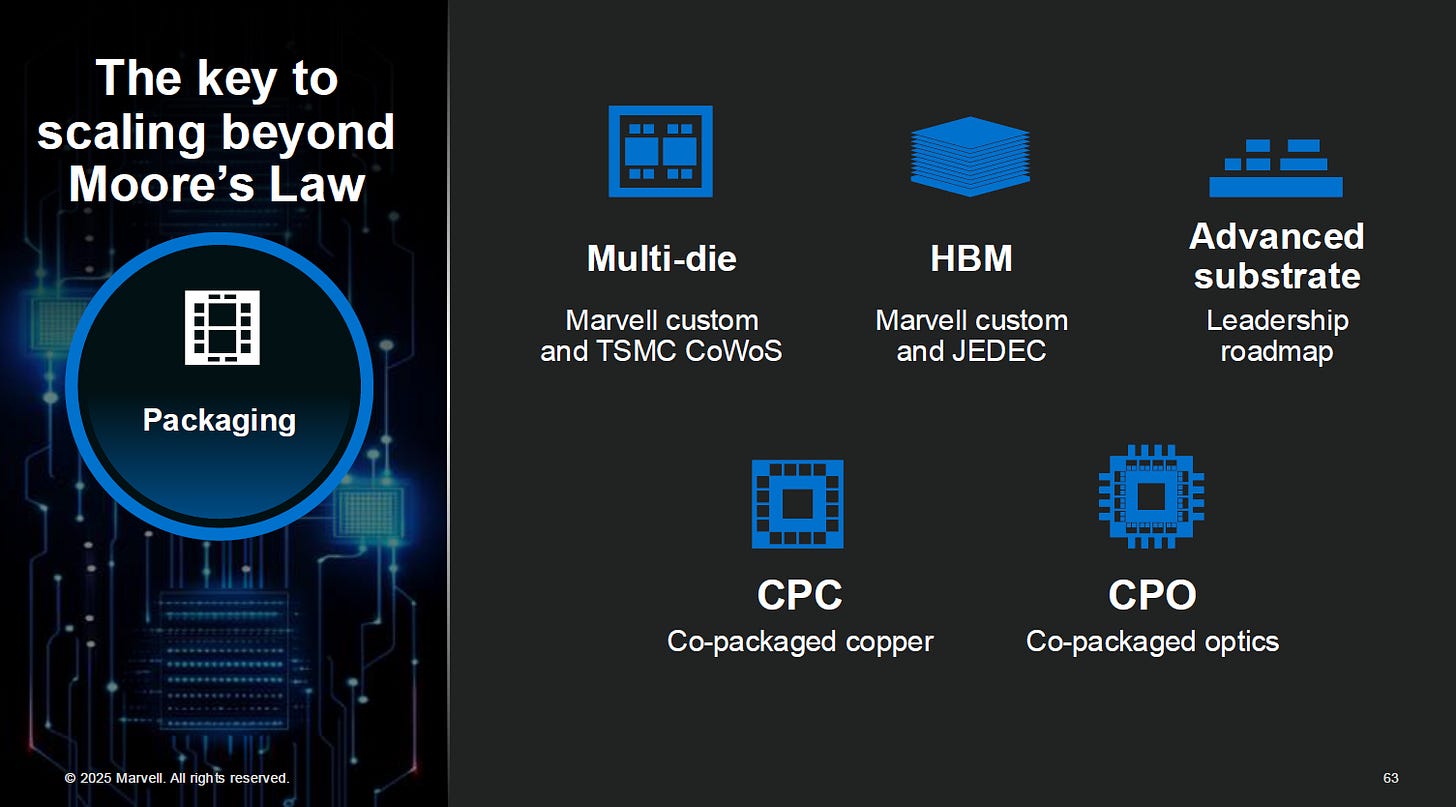
Advanced Packaging: Integrates fan-out, 2.5D, CoWoS, and CPO to increase system density and efficiency.
Manufacturing Logistics: Bridges wafer-level manufacturing and system-level SMT assembly for streamlined supply chains.
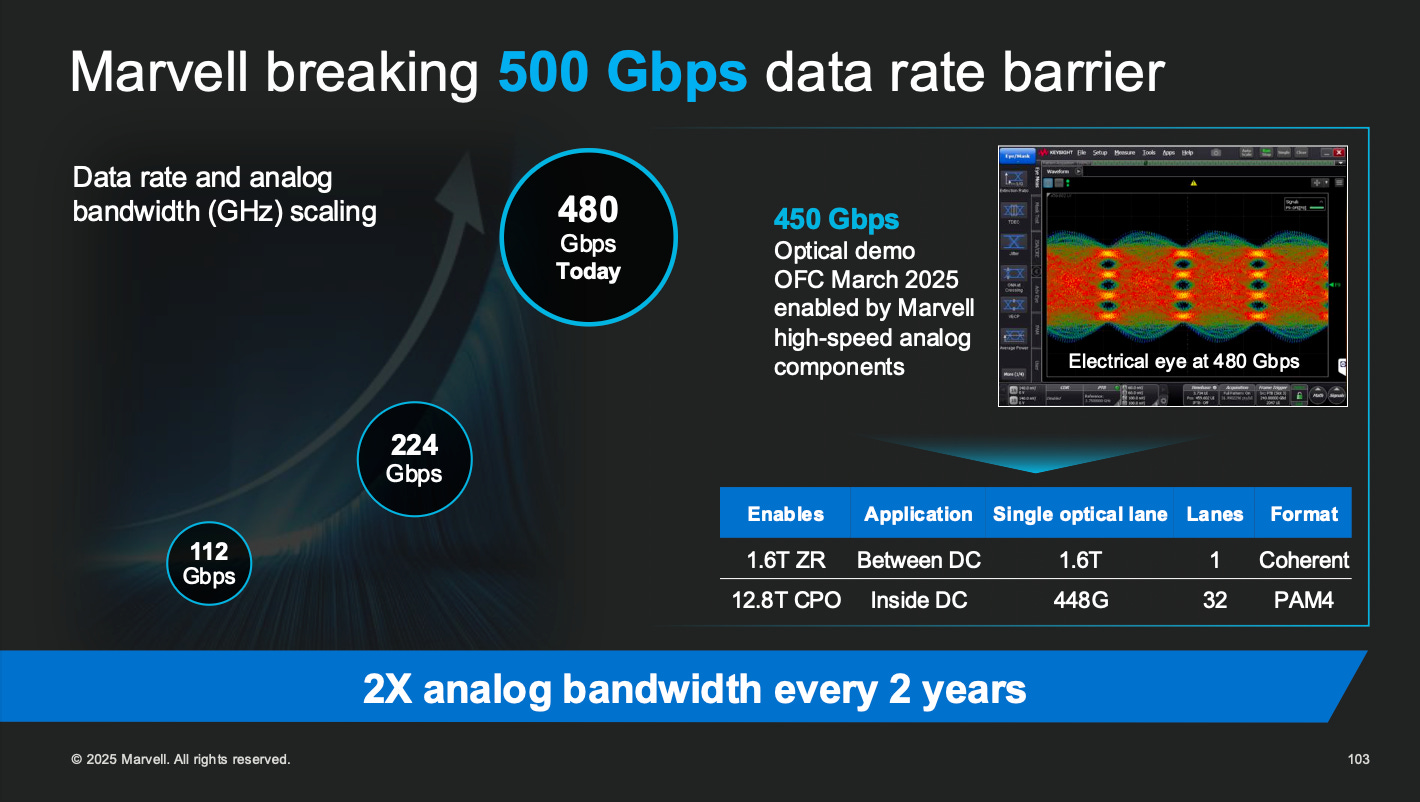
At OFC 2025, Marvell unveiled the world’s first 448G electrical-optical SerDes, supporting next-gen optical interconnect architectures such as CPO, LPO, and OIO. This technology underpins scalable, low-latency, and energy-efficient AI system architectures across rack-to-rack and pod-to-pod deployments.
SRAM and HBM Advancements Paving the Way for Heterogeneous Integration
Memory architecture remains a critical bottleneck for AI chips. In advanced logic nodes, SRAM’s area and power usage become increasingly significant. Marvell addresses this with custom SRAM designs that deliver:
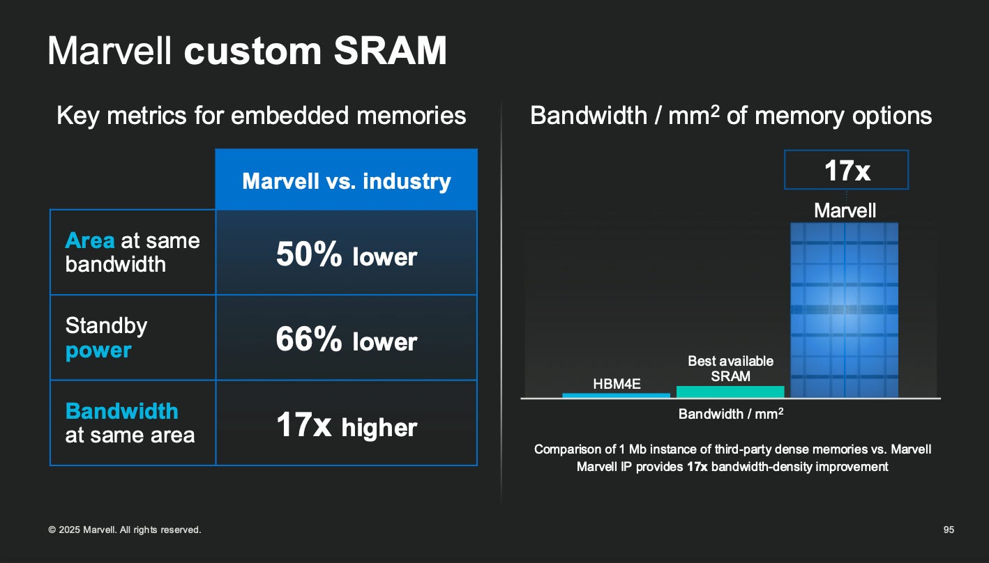
50% smaller area for the same bandwidth
66% lower standby power
17x bandwidth density at the same area
These features are highly suitable for L2/L3 caches, neural caches, and inference weight buffers, and are already integrated into leading AI accelerator designs.
In parallel, Marvell is developing custom HBM systems tightly coupled with its CPO-based photonic packaging platforms. This approach forms a high-performance memory foundation optimized for heterogeneous integration, NoC (Network-on-Chip), and scale-up fabric, enabling low-latency, high-throughput, and scalable compute infrastructure for data centers.
Toward Platform-Centric Chip Design
Marvell’s 2025 technology roadmap outlines three critical vectors for the evolution of accelerated computing:
The shift from single GPU dominance to customizable XPU system architectures
The transition from electrical SerDes to integrated optical interconnects
The move from standard SRAM to custom memory and high-density packaging integration
These trends reflect a fundamental transformation—from point optimization to full-stack system-level design. Only with vertically integrated capabilities in process technology, IP, packaging, and interconnects can future AI infrastructure meet the scale, efficiency, and flexibility required in the Angstrom era.
For Marvell, chips are not just functional units—they are the architectural foundation of tomorrow’s data centers.
For Paid Members, SemiVision will discuss topics on
From Vision to Reality: Marvell’s Transformation Through Cloud-Optimized Silicon
Marvell 2025: Leading the New Era of AI Infrastructure with Full-Stack Technology and Custom Silicon Strategy
Strategic Moves by the Traditional Hyperscalers
The Rise of Emerging Hyperscalers
XPU and Attach Strategy: Marvell’s Dual-Axis Expansion
Decoding the Full Picture Through Sockets: How Marvell Defines Its Influence in the AI Chip Era
Technology Leadership: Comprehensive Deployment Across SerDes, Die-to-Die, and Co-Packaged Optics
Marvell’s Full-Service Offering for AI Chips and Solutions
Why Marvell Wins
Process: From Nanometers to the Ångström Era
IP: World’s First 448G Electrical and Optical SerDes
Packaging: Entering the Battlefield of Advanced Integration
Driving Cross-Generational Success Through Technology
Custom SRAM and HBM: The Architecture Advantage
Custom Memory Strategy as a Core Growth Engine
Marvell’s Business Model and Strategic Shift in Design
Forward-Looking Roadmap: From 3nm to 2nm and the Ångström Era
XPU Attach: The Critical Sibling to XPU in the Modular AI Era
SerDes, Die-to-Die, and Co-Packaged Optics Technologies
Evolution of the Silicon Photonics Platform and Innovations in Advanced Packaging (2.5D, 3.5D, 4.5D)
Impact of Custom SRAM and HBM Architectures on AI Platforms
Facing the Slowdown of Moore’s Law: Marvell’s Platform Strategy for Advanced Process and IP Readiness


2025年2月28日

2025年6月2日

2025年5月21日

2025年5月6日

2025年6月28日

2025年5月6日
2025年7月8日

2025年7月4日

2025年6月4日
From Vision to Reality: Marvell’s Transformation Through Cloud-Optimized Silicon
At its 2021 Investor Day, Marvell unveiled a transformative vision anchored in a strategic shift toward“The Era of Cloud-Optimized Silicon.”This marked a departure from the traditional paradigm of “x86 CPUs for everything,” predicting that future cloud architectures would be defined by heterogeneous compute and deeply integrated custom silicon. Four years later, this vision has been fully realized—positioning Marvell as a strategic leader in AI and high-performance data center markets.
The Three-Stage Vision from 2021
In that presentation, Marvell outlined a clear three-phase evolution in data center infrastructure:
Software on x86 for Everything: The legacy model, where all workloads ran on general-purpose CPUs—resulting in limited system flexibility and underutilized resources.
Heterogeneous Computing: The rise of AI and data explosion drove the adoption of specialized accelerators like GPUs, FPGAs, and DPUs, forming a heterogeneous compute environment.
Cloud-Optimized Silicon: The final phase where cloud providers and semiconductor firms co-develop custom silicon—such as custom CPUs, ML accelerators, and DPUs—becomes the foundation of next-generation data centers.
This model anticipated tight coupling between compute and data, increasing diversity in accelerator architectures, and the rapid evolution of SoC and advanced packaging technologies.
2025: Delivering on the Vision
By 2025, Marvell not only fulfilled this roadmap—it had already advanced on multiple fronts, demonstrating exceptional strategic foresight and execution:
- Commercialization of Custom Cloud Silicon
Marvell launched multiple custom CPU, ML, and DPU solutions tailored for hyperscale cloud workloads, including inference, data movement, and secure processing. These chips adopted modular chiplet-based packaging and integrated high-speed SerDes, Co-Packaged Optics, and Die-to-Die (D2D) connectivity—enabling highly efficient, scalable, and power-optimized heterogeneous platforms.
- Co-Packaged Optics and Optical I/O as Core Technologies
Marvell’s silicon photonic engines entered volume production, becoming integral to customer AI accelerators and server architectures. In bandwidth-heavy scenarios like 1.6Tbps and 6.4Tbps optical modules, Marvell showcased superior energy efficiency and packaging integration, addressing the limitations of traditional electrical interconnects.
- Multi-Die Packaging and 2nm Process Realization
Marvell successfully adopted 2nm process nodes and implemented 3D packaging with bidirectional D2D communication, delivering seamless connectivity for heterogeneous compute elements. These advanced technologies power not only Marvell’s own ASICs but also support customers through its standardized, platform-oriented design ecosystem.
- Platform-Centric Design and Deep CSP Collaboration
Unlike traditional IP vendors, Marvell operates as a platform partner, providing end-to-end support across design, packaging, and validation. This approach has enabled close collaborations with the top four CSPs—Google, Amazon, Microsoft, and Meta—allowing Marvell to penetrate key segments like AI accelerators, LPO modules, and data center switches with agility and precision.
Four Years of Validated Vision
What Marvell foresaw in 2021—the convergence of data center architecture and chip design—has become a reality in 2025. Through early investments in silicon photonics, packaging platforms, and the XPU Attach strategy, Marvell has positioned itself at the center of the AI data infrastructure surge.
Marvell’s journey is a case study in foresight, execution, and platform-driven transformation. It presents a compelling alternative path for the semiconductor industry: not just selling chips, but co-defining the future of cloud infrastructure.。


Marvell 2025: Leading the New Era of AI Infrastructure with Full-Stack Technology and Custom Silicon Strategy
As generative AI and large language models continue to drive exponential growth in data center compute demands, Marvell’s 2025 investor presentation clearly articulates its vision and execution: by integrating SerDes, silicon photonics, HBM, advanced packaging, and fully customized chip platforms, Marvell is expanding its footprint in the AI infrastructure market. Positioned as a critical enabler of high-speed interconnects and tailored compute solutions, Marvell aims to play a central role in shaping the AI datacenter landscape through 2030 and beyond.
- Capex Expansion and TAM Surge in the AI Era


In 2025, the infrastructure behind AI data centers is undergoing unprecedented capital investment growth. The four major U.S. hyperscalers—Amazon, Microsoft, Google, and Meta—are aggressively expanding their next-generation AI computing platforms. At the same time, a wave of emerging hyperscalers is rising rapidly, engaging in full-stack initiatives spanning model development, vertical applications, and sovereign AI platforms, signaling the advent of a new platform-driven era in AI infrastructure.
Strategic Moves by the Traditional Hyperscalers
Amazon (AWS)continues to develop its Trainium and Inferentia chips, enhancing its AI training clusters and data lake systems with a focus on silicon autonomy and cloud-scale AI services.
Microsoft (Azure)is deepening its collaboration with OpenAI while advancing in-house development of the Maia AI accelerator and Cobalt CPU. Its infrastructure also supports the backend of its Copilot AI tools ecosystem.
Google (GCP)builds a large-scale, multi-tenant AI cloud based on its TPU and Pax architecture, supporting both proprietary Gemini models and open-source deployment options.
Metais focused on Llama and other foundation models, deploying its MTIA chips and scaling out next-gen AI data centers to power AI-driven social platforms and AR/VR integration.
These players are transitioning from “GPU stacking for performance” toward AI-native hardware and photonic-electronic integration. Key technologies such as silicon photonics, co-packaged optics (CPO), and 3D ICs are now being deployed to reduce power consumption and optimize latency.
The Rise of Emerging Hyperscalers
Beyond the incumbents, Marvell identifies three fast-emerging hyperscaler categories:
Model-Driven Players (e.g., xAI, OpenAI):Focused on in-house LLM development, these companies are increasingly taking ownership of AI training and inference infrastructure.
Application-Driven Leaders (e.g., Tesla, Apple):These firms embed AI into automotive, mobile, and edge systems, driving hybrid deployments with low-latency, on-premise, and edge-cloud coordinated data center architectures.
Sovereign AI Innovators (e.g., Humain, Stargate):Building proprietary data, models, and custom silicon to meet government, defense, and national data sovereignty demands. These players challenge the prevailing open-source and shared-infrastructure paradigms with closed-loop AI stacks.
These new entrants are pushing beyond model innovation into deep vertical integration—spanning chips, packaging, networking, and thermal management—making them key partners and competitive forces for upstream providers like Marvell, TSMC, and NVIDIA.
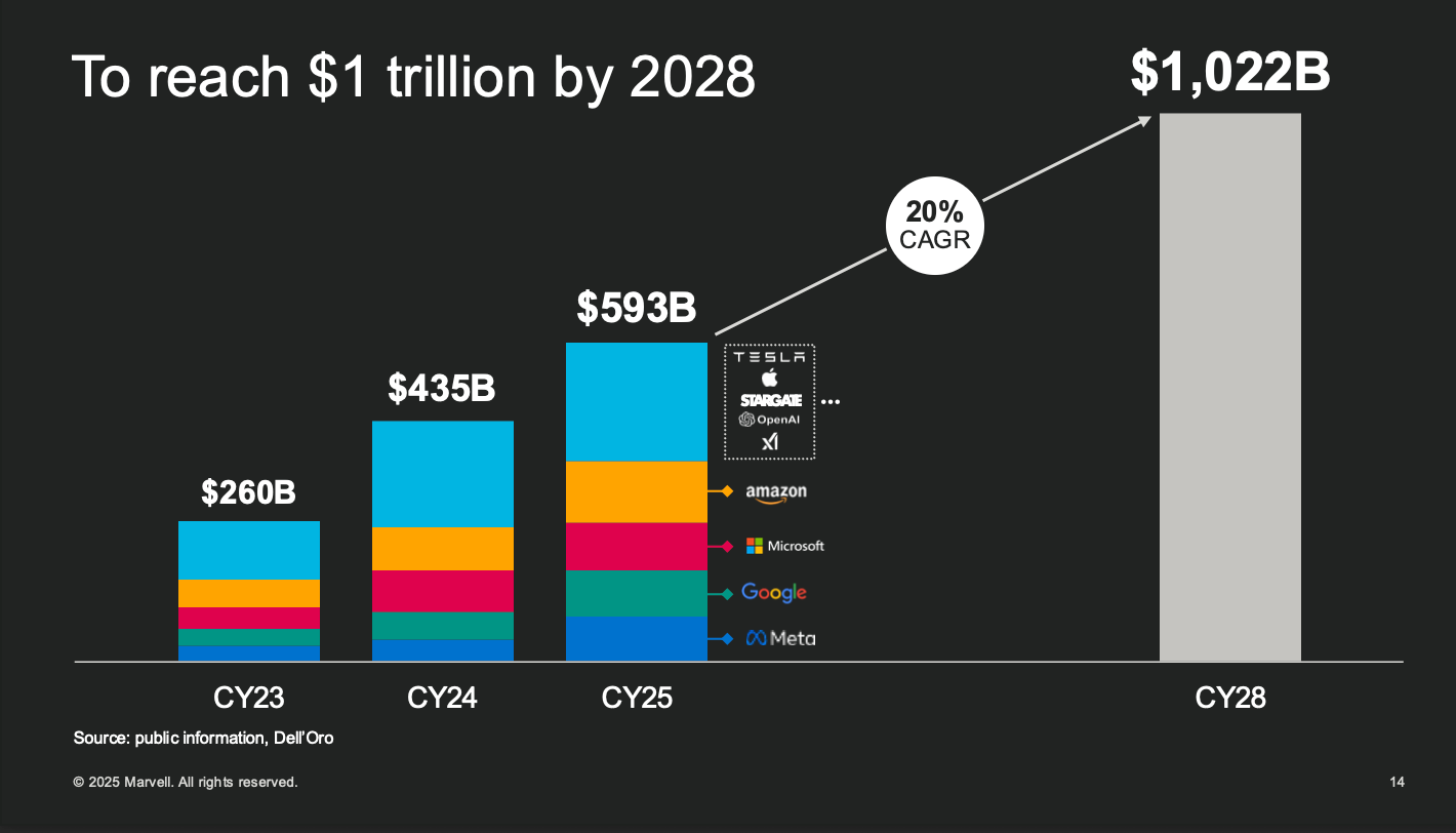
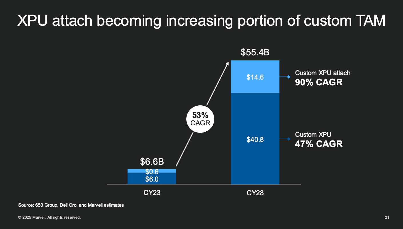
Between 2023 and 2025, the top four hyperscalers are increasing CAPEX at a 46% CAGR, reaching $327 billion. Overall data center investments are expected to rise from $260 billion in 2023 to $593 billion in 2025, and to surpass $1 trillion by 2028. Marvell estimates the total addressable market (TAM) for data center semiconductors will grow from $21 billion in 2023 to $94 billion in 2028. Of that, the Accelerated Custom Compute segment is expected to expand at a 53% CAGR, reaching $55.4 billion.

XPU and Attach Strategy: Marvell’s Dual-Axis Expansion
Against the backdrop of rapidly scaling AI data centers, the trend ofCustom XPUdevelopment is becoming increasingly pronounced. As GPU costs soar and supply remains constrained, more cloud providers and hyperscale platforms are turning to in-house AI accelerator development to gain flexibility and cost-efficiency. While NVIDIA’s GPUs continue to lead in both inference and training performance, their high unit cost and platform lock-in have motivated the industry to explore alternative architectures—sparking a wave ofin-house ASIC development.
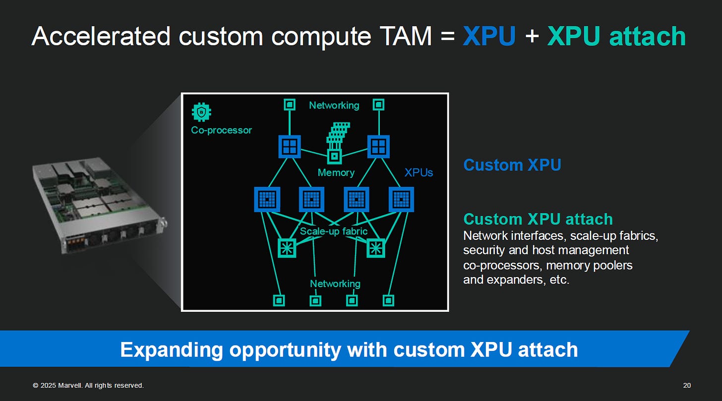
The concept of Custom XPU encompasses not only customized CPUs, GPUs, DPUs, and NPUs, but alsosystem-level attach componentswithin heterogeneous compute frameworks. These includescale-up fabrics,memory pooling units,co-processors,security modules, andoptical interconnects. The focus shifts from merely maximizing individual chip performance toco-optimizing at the system architecture level.
In this architectural transition,Marvell plays a pivotal roleas an enabler across three core competencies:
Advanced Logic Process Capability:
Marvell has a proven track record in designing custom ASICs at sub-5nm nodes and is actively engaging with leading foundries like TSMC on N3 and N2 processes. This enables the delivery of high-performance, low-power chips tailored for AI inference, networking, and security workloads.
Advanced Packaging and Integration:
Leveraging chiplet-based design and 2.5D/3D advanced packaging, Marvell can integrate compute dies with high-speed SerDes, HBM stacks, and optical modules within a single package. This significantly reduces latency and power consumption while enhancing system bandwidth density.
High-Speed SerDes and Optical Interconnect Expertise:
Marvell leads in high-speed I/O with its 112G and 224G SerDes technologies, as well as full-stack support for PCIe Gen6, CXL, and Ethernet. It is also deeply invested in optical interconnect technologies, supporting bothCo-Packaged Optics (CPO)andLinear-Drive Pluggable Optics (LPO)to future-proof data center bandwidth scaling.
In essence, the Custom XPU strategy is not merely a cost-cutting approach—it is afundamental shift toward infrastructure co-design, where performance, power, and flexibility are achieved through holistic silicon-system-package integration. Marvell’s vertical stack of competencies across logic, packaging, and I/O makes it an indispensable partner to both traditional cloud hyperscalers and emerging AI-native platforms. In this new paradigm, the value of AI hardware transcends standalone chip metrics and moves towardmodular, customizable, and scalable system design.
Marvell clearly distinguishes the accelerated compute market into two main segments: the Custom XPU—referring to the core custom accelerator itself—and the XPU Attach, which includes peripheral co-processing chips such as network interfaces, scale-up fabrics, memory controllers, and management modules.
Decoding the Full Picture Through Sockets: How Marvell Defines Its Influence in the AI Chip Era
As AI data centers shift toward heterogeneous computing and platform-based design, relying on a single chip’s performance is no longer sufficient to meet the demands of large-scale AI models. Marvell, through its dual-track strategy of “Custom XPU + XPU Attach,” is reshaping the competitive landscape of accelerated computing. Its 18Accelerated Custom Compute Socketsdisclosed in 2025 not only reflect the depth and breadth of its technical deployment but also serve as a concrete metric for assessing its maturity and strategic penetration in the AI chip business.
- Total Socket Count: A Quantitative Measure of Platform-Level Collaboration
The 18 sockets announced by Marvell do not simply represent 18 ASICs. Instead, they denotereal-world deployments with customers, each being asocket-level design projectwith commercial value and deep system integration.
Each socket corresponds to a co-defined chip project with a hyperscaler or emerging AI player, potentially including:
Custom AI training or inference accelerators (Custom XPUs)
Scalable memory and network co-processors (Attach ASICs)
Optical transceiver controllers and SerDes PHYs
DPUs, scale-up fabric controllers, and secure I/O components
These are not one-off designs, but multi-year, multi-generational engagements reflecting Marvell’s strategic role in helping shape next-generation AI system blueprints.
- Dual Market Penetration: Top Hyperscalers and Emerging AI Players
According to Marvell’s data, the 18 sockets are distributed across two key segments:
Top 4 U.S. Hyperscalers(Amazon, Microsoft, Google, Meta)
3 Custom XPU Sockets: These represent Marvell’s direct involvement in designing core compute units like training or inference ASICs.
9 Custom XPU Attach Sockets: These support critical subsystems such as SerDes, CXL interfaces, memory controllers, packet processing, and optical connectivity.
Emerging Hyperscalers(e.g., OpenAI, Tesla, xAI, Humane)
2 Custom XPU Sockets: Reflecting a trend toward self-defined chips and custom acceleration platforms by new AI-native entrants.
4 Custom Attach Sockets: Supporting modular I/O, memory disaggregation, and cloud-edge collaborative deployments.
This diversified customer base highlights Marvell’s unique ability to serve both established and next-generation hyperscale platforms.
- Strategic Implications: From IP Vendor to System-Level Partner
These socket projects are not short-term engagements—they representmulti-generational design partnerships. Marvell is no longer just an IP supplier; it has become a full-stack enabler involved in every layer of chip design—from architectural co-definition and advanced packaging to SerDes and thermal/power co-optimization.
More importantly, the success of these sockets reflects the growingmodular and platform-based nature of AI hardware. Through its integration of ASIC design, packaging technology, and high-speed interconnects, Marvell provides end-to-end, co-optimized silicon platforms tailored for cloud and emerging AI architectures.
In this context, Marvell is playing the role ofinfrastructure builder and ecosystem integratorfor the AI chip era—delivering scalable, reusable, and customizable solutions. These socket engagements offer a more comprehensive metric than traditional product counts. In today’s AI landscape,owning more socketsdoesn’t just signal market share—it defines who shapes the future of AI infrastructure.
Technology Leadership: Comprehensive Deployment Across SerDes, Die-to-Die, and Co-Packaged Optics
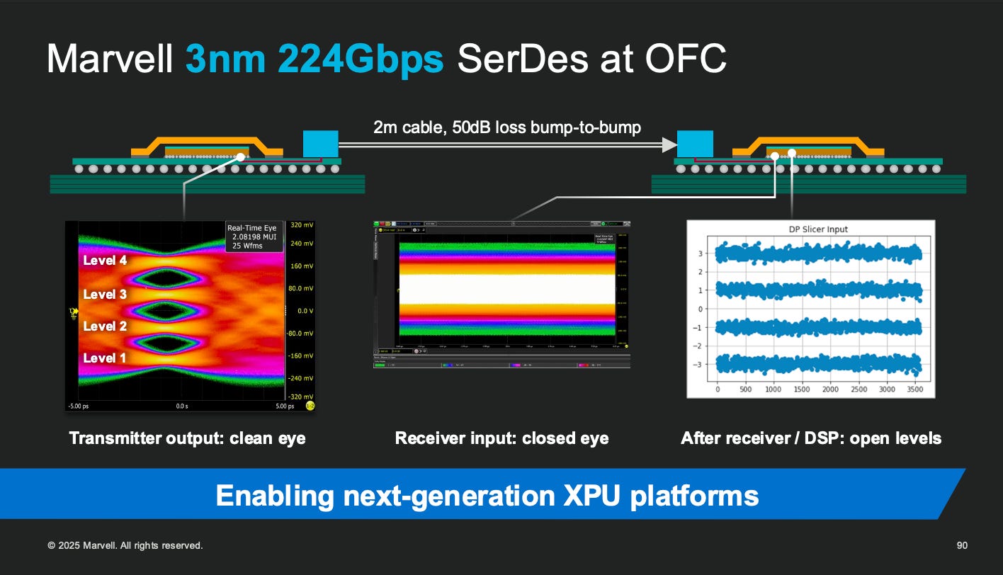
Marvell highlights its sustained generational leadership inSerDes technology, with its 3nm 224Gbps SerDes—showcased at OFC 2025—andMarvell is planning next-generation SerDes architectures targeting bandwidth densities exceeding 50 Tbps/mm² and energy efficiencies below 0.1 pJ/bit. This positions it ideally for ultra-long-reach, high-precision AI data center interconnects.
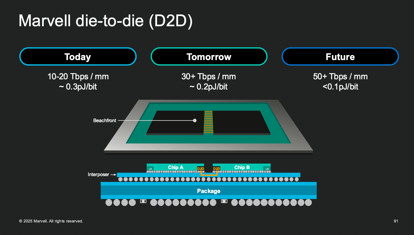
Inchip-to-chip interconnect, Marvell’sDie-to-Die (D2D)technology is progressing toward50Tbps/mmperformance withsub-pJ/bit energy efficiency, enabling tight integration acrossmulti-die packaging platforms, such asmulti-stack HBM systemsandCoWoS.
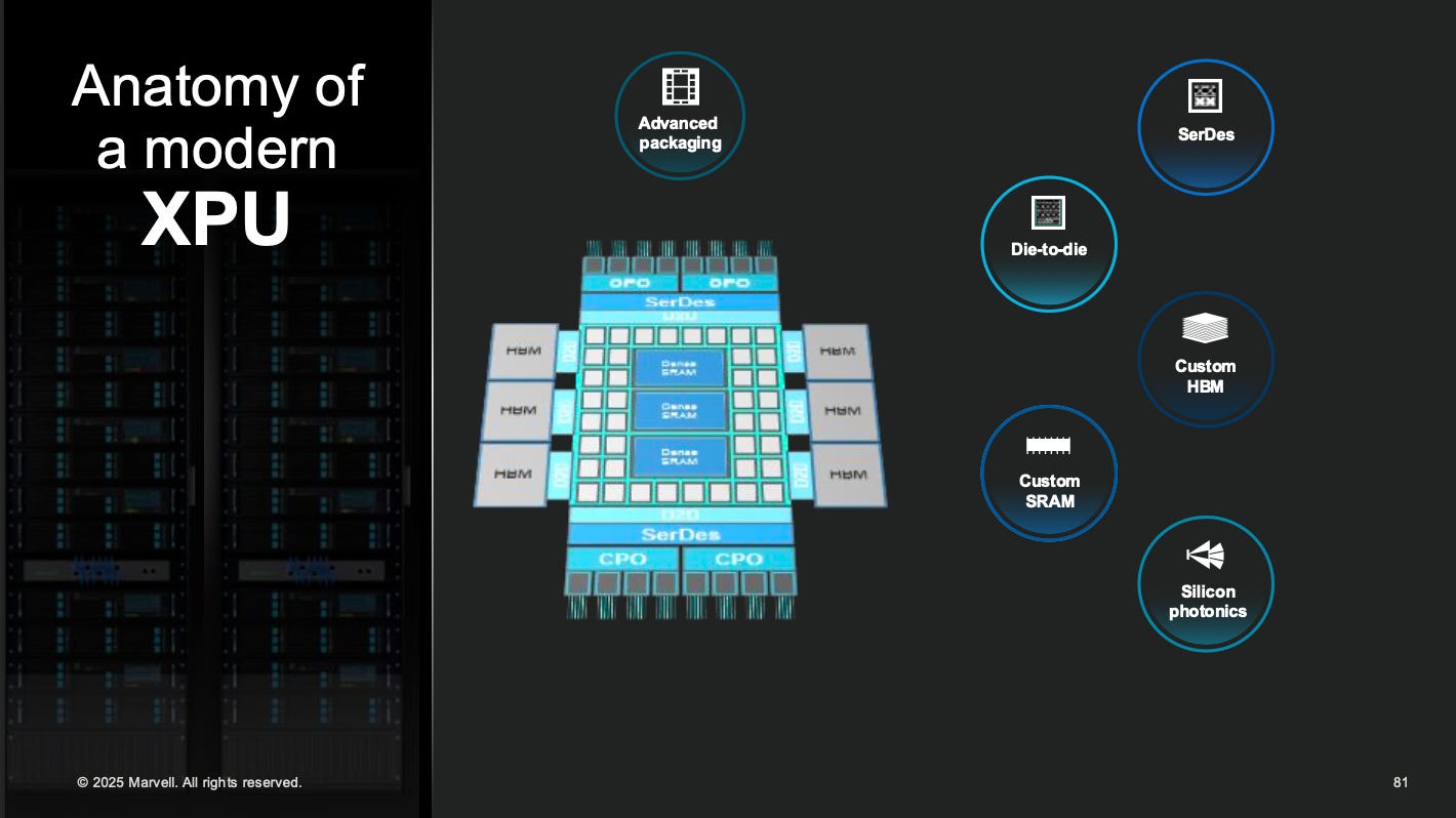
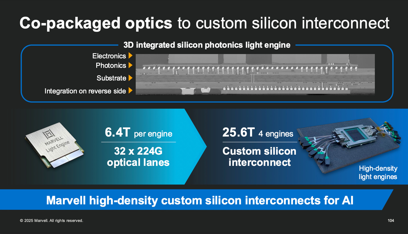
In the optical domain, Marvell has established an in-houseCo-Packaged Optics (CPO)platform built on its proprietarysilicon photonics engine, delivering6.4Tbps per engine, with scalability up to25.6Tbpsvia a 4-engine configuration. The platform isaligned with TSMC’s advanced packaging processes and JEDEC standards, reinforcing its role as a next-generation infrastructure enabler.
Marvell’s Full-Service Offering for AI Chips and Solutions

Marvell’s ability to win in today’s AI custom silicon market stems from its unique“Full-Service Custom” model—not merely as an IP provider or standalone ASIC design house, but as acomprehensive integration partnerthat enables hyperscalers and emerging AI players to transform system architecture visions into production-ready silicon.
- System Architecture
Marvell collaborates with customers to co-developcomplete system architectures, rather than just delivering IP blocks. Based on the AI workload profile—be it training or inference—Marvell works on memory access patterns, interconnect topologies, and power-performance trade-offs to co-design multicore compute, network transport, and dataflow control blueprints.
➡Key Advantage: Truesystem-level thinking, enabling next-gen platform definition in partnership with cloud providers.
- Design IP
Marvell offers a full suite of advanceddesign IPs—including high-speed I/Os, SerDes, PCIe, CXL, and Coherent Fabric—ready to be embedded into custom ASICs. This ensures short time-to-market and high reliability in silicon development.
➡Key Advantage:In-house SerDes/CXL IP portfolio, enabling rapid support for high-bandwidth AI chip interconnects without overreliance on third-party licensing.
- Silicon Services
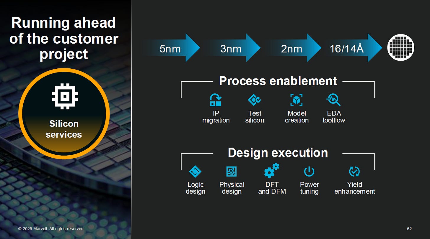
From RTL and Physical Design (PD) to DFT, Timing Closure, and Tape-out, Marvell providesend-to-end silicon implementation services. The company is already production-proven on advanced nodes like 5nm and 3nm and is actively preparing for 2nm designs.
➡Key Advantage: Marvell can help customers tape-out quickly at advanced nodes (e.g.,TSMC N3B/N2) while supporting late-stage PPA optimization.
- Packaging
As chiplet architectures and optoelectronic integration become mainstream, Marvell supportsadvanced packaging technologiesincluding 2.5D interposers, fan-out, heterogeneous integration, and optical engine packaging.
➡Key Advantage: Co-design of SerDes/CPO components with packaging forlow-power, high-bandwidth, and reliable interconnectsolutions.
- Manufacturing and Logistics
Marvell delivers aturnkey manufacturing and logistics solution—covering wafer production, packaging, testing, and final delivery. Especially for cloud-scale ASIC programs, Marvell streamlines the supply chain and accelerates production ramps.
➡Key Advantage: Provenmass production and delivery execution, eliminating the need for hyperscalers to manage complex backend operations.
Why Marvell Wins
Marvell’s ability to span thissystem-to-silicon-to-packagingcontinuum is what makes it indispensable in enabling the rise of custom XPUs and attach components in the AI era.
Process: From Nanometers to the Ångström Era
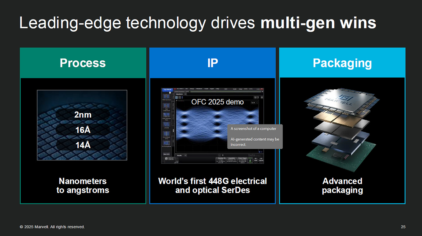
Marvell has fully entered the 2nm design node and revealed that its future roadmap includes advanced nodes such as 16Å and 14Å. This signifies a close collaboration with leading foundries like TSMC and demonstrates Marvell’s capability in ultra-high-density logic integration and power efficiency optimization—meeting the extreme performance demands of AI accelerators, SerDes, and high-speed memory interfaces.
➡Technical significance: Enables support for cutting-edge process needs from hyperscalers, achieving competitive advantages in HBM integration, high-frequency SerDes, and logic density scaling.
IP: World’s First 448G Electrical and Optical SerDes
At OFC 2025, Marvell showcased the world’s first 448G-capable SerDes IP, supporting both electrical and optical signal transmission. This represents a major technological milestone for Co-Packaged Optics (CPO), optical engines, and silicon photonics platforms.
➡Technical significance:
Bandwidth breakthrough: 448G per channel sets a new bar for data throughput, serving as the foundation for next-generation CXL and AI fabrics.
Packaging and photonic integration: The IP integrates seamlessly with Marvell’s optical modules and advanced packaging platforms (e.g., InFO, CoWoS, LGA).
Packaging: Entering the Battlefield of Advanced Integration
The visual in Marvell’s presentation illustrates a typical 3D packaging stack, potentially including:
HBM memory stacks
Compute chiplets (XPU cores)
Optical/SerDes I/O dies
2.5D interposers or RDL-based integration
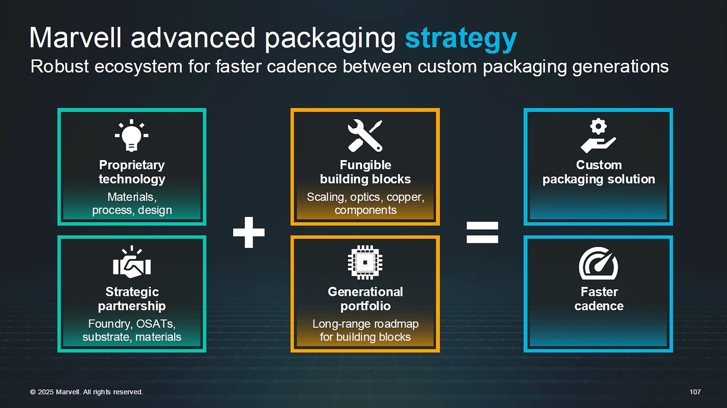
Marvell, through partnerships with TSMC and other packaging leaders, offers a full range of packaging technologies—from fan-out to CPO, silicon photonic integration, and even System-on-Wafer (SoW) level solutions.
➡Technical significance: Comprehensive stack integration that enables CPO, heterogeneous integration, and AI inference accelerator deployment.
Driving Cross-Generational Success Through Technology
The core message of this graphic is that Marvell is not merely a component supplier—it leads the industry in all three foundational technological dimensions:
Process: Enables breakthroughs in logic density and energy efficiency.
IP: Next-generation SerDes and optical interconnects for future system fabrics and CPO architectures.
Packaging: Delivers scalable physical integration for high-performance, energy-efficient system deployment.
This leadership has allowed Marvell to secure long-term, multi-generational custom platform design engagements with top hyperscalers—cementing its critical role in the custom XPU ecosystem.
Custom SRAM and HBM: The Architecture Advantage
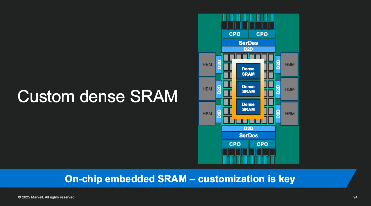
SRAM (Static Random-Access Memory) remains a critical benchmark in logic process advancement. Whether for CPUs, XPUs, AI accelerators, or memory controllers, overall area, power consumption, and bandwidth are often limited by embedded SRAM performance. As process nodes advance into the 3nm, 2nm, and ultimately Ångström era, SRAM scaling has lagged significantly behind logic density improvements—exacerbating the energy and memory bottlenecks in modern chips.
To address this challenge, Marvell has broken away from the conventional IP model by pioneeringcustom SRAM development, creating highly tailored, high-density, and low-power embedded memory solutions. According to its latest disclosures, Marvell’s custom SRAM achieves50% area reductionat the same bandwidth,66% lower standby power, and up to17× bandwidth densityimprovement in the same footprint—far exceeding current commercial SRAM and HBM4E combinations. This reflects disruptive potential for embedded memory in data-intensive applications.
In parallel, Marvell is advancingcustom HBM subsystem design, where logic cores (XPUs) are modularly integrated with high-speed wideband memory through CPO, SerDes, and Die-to-Die (D2D) interconnects. This not only supports traditional DRAM-based memory hierarchies but also paves the way forchiplet-based heterogeneous integration—ideal for generative AI, large language model inference, and high-performance computing systems.
Custom Memory Strategy as a Core Growth Engine
Through its dual-track strategy of custom SRAM and HBM integration, Marvell is leveraging its strengths in process technology, advanced packaging, and optical interconnects to drive the next generation of AI chip platforms. By optimizing energy efficiency, data access, and spatial density at the system level, Marvell is positioning itself as a foundational force powering the evolution of AI-centric datacenter infrastructure.
Marvell’s Business Model and Strategic Shift in Design
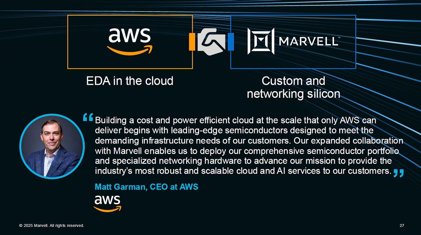
To date, Marvell has securedmulti-billion-dollar custom partnershipswith customers such asAWS, Microsoft, Meta, and xAI, and continues to expand both the number of active sockets and deployed platforms year over year.
Forward-Looking Roadmap: From 3nm to 2nm and the Ångström Era
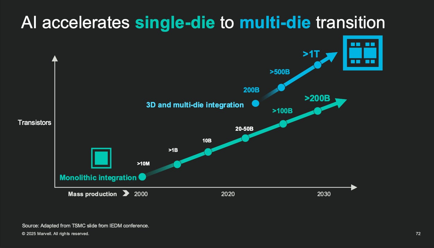
Marvell has announced thecompletion of IP validation and production readiness for its 2nm and 16Å-class platforms. Starting in 2025, the company is actively advancingCustom SRAM and Co-Packaged Optics (CPO) architecturesbased on the 2nm node, laying the groundwork forfuture AI systems exceeding one trillion transistors and rack-scale computing demands.
SemiVision conducts an in-depth analysis on selected technical aspects
XPU Attach: The Critical Sibling to XPU in the Modular AI Era
- XPU vs. XPU Attach: System Role and Scalability
Marvell divides the custom compute ecosystem into two main categories:XPU(main compute chips like CPUs, GPUs, and accelerators) andXPU Attach(companion chips that provide networking, memory, management, and I/O functionalities). While the XPU serves as the core compute engine, the XPU Attach encompasses elements such as network interfaces, memory controllers, system management co-processors, and security/compression engines to enhance overall system performance.
According to Marvell, the custom XPU market is expected to reach$40.8 billionby 2028, with a CAGR of47%. However, the XPU Attach segment is growing even faster, with an estimatedCAGR of nearly 90%. Out of Marvell’s 18 custom ASIC deployments to date, 3 are XPU designs and 9 are Attach chips from hyperscaler projects; emerging clients account for another 2 XPU and 4 Attach chips—indicating thatover two-thirdsof deployments are Attach-class components.
In the evolving server landscape, these companion chips are becoming central to architectural design. They offer critical functionality in high-bandwidth connectivity, memory pooling, system-level security, and performance optimization. Marvell supports a full-stack solution—from rack-level collaboration to IP design, advanced packaging, and high-volume manufacturing—enabling clients to build customized systems rapidly.
- XPU Attach: Enabling the Future of Modular AI Architecture
As AI chips evolve towardmodular and heterogeneous integration, XPU Attach components are emerging askey enablersof performance scaling and system-level cohesion. While the market once focused solely on the main compute dies (e.g., GPU, NPU, DPU), it’s now evident that the supporting infrastructure—high-speed interconnects, memory orchestration, I/O, and security—is vital to platform performance.
From Compute-Centric to System-Centric Thinking
Historically seen as secondary players, companion chips are now essential in data-intensive, high-throughput AI systems. Without robust support from SerDes interfaces, optical transceiver controllers, memory access units, or PCIe/CXL engines, even the most powerful accelerators will underperform.
XPU Attach now includes:
Memory controllers and coherence engines
High-speed interconnects(SerDes, PCIe, CXL)
Network packet processors and cooperative accelerators
Power and system management, security, and configuration chips
Together, these modules support throughput, synchronization, and platform reliability at scale.
- Market Outlook: Attach Growing Faster than XPU
The XPU Attach market is outpacing the core XPU segment. By 2028, it is expected to reach$14.6 billion, with a staggeringCAGR of 90%. In Marvell’s 18 deployed sockets, only 5 are main XPU devices while the remaining 13 are Attach chips. Furthermore, out of 50+ potential engagements in the pipeline, nearlytwo-thirdsare Attach-oriented—highlighting growing demand for modular companion chips.
- Technical and Strategic Value of Attach
The rise of Attach brings several strategic advantages:
Performance upliftby offloading I/O and memory functions from the main XPU
System complexity reductionwith pre-integrated control and communication modules
Accelerated time-to-marketthrough modular platform architectures
Higher gross marginopportunities for ASIC vendors due to standardized IP reuse
- Marvell’s Strategy: Leading through Attach
Unlike players who focus purely on core compute,Marvell’s strategy centers on Attach—providing collaborative components that integrate seamlessly with any XPU, including those from third-party vendors. This allows Marvell toparticipate deeply in AI platform designwithout having to compete directly in the XPU race.
Its Attach portfolio—featuringhigh-speed SerDes, CPO optical modules, and HBM memory controllers—forms a coherent solution stack for scalable, high-efficiency data infrastructure.
Modular AI Platforms and the Rise of Attach
The AI chip market is transitioning frommonolithic superchipstomodular, disaggregated systems. XPU Attach is central to this evolution. These companion chips inject performance, flexibility, and integration efficiency into next-gen platforms while opening new avenues for innovation and commercial success.
Marvell’s deep investment in Attach technology positions it as a pivotal playerin tomorrow’s AI infrastructure, ensuring it plays a central role in the ongoing transformation of data center compute architectures. As data flows continue to surge, the importance of Attach components will only increase—ultimately standing alongside XPU cores as equal pillars of AI compute platforms.


SerDes, Die-to-Die, and Co-Packaged Optics Technologies

As AI training and cloud computing workloads surge, interconnect interfaces must break past existing limitations. Marvell is at the forefront, developing advanced DSP-based SerDes at the 3nm process node, achieving per-channel speeds of 200–224Gbps to support cross-card and inter-host connectivity. In a DesignCon demonstration, Marvell showcased its 224G long-reach SerDes transmitting at 200Gbps per lane over 2-meter copper cables—nearly double the bandwidth of traditional 100G links. These high-end SerDes require powerful equalization and low-loss channel design to overcome severe signal attenuation at ultra-high frequencies across cables and sockets. By leveraging advanced DSP techniques, Marvell’s SerDes receivers reconstruct signals with closed eye diagrams, enabling meter-scale transmission with up to 50dB insertion loss—without data loss.
Die-to-Die (D2D) connectivity represents both a challenge and a breakthrough. Marvell targets a die-to-die bandwidth density of 50Tbps per millimeter and energy efficiency below 0.1pJ/bit. On the 2nm platform, Marvell recently demonstrated a bi-directional 3D die stacking interface reaching 6.4Gbps per channel. This theoretically doubles the bandwidth and halves the pin count when assembling multi-die systems using 2.5D, 3D, or 3.5D configurations. Such advanced packaging connectivity is critical to minimizing inter-core distances and increasing memory-compute density.
In the Co-Packaged Optics (CPO) domain, Marvell integrates silicon photonics engines with chip-level packaging to enable ultra-long-reach, high-bandwidth connections. Its custom AI acceleration architecture combines XPU compute dies, HBM, and other chips with Marvell’s 3D silicon photonics engine on a single substrate, connected via high-speed SerDes, D2D links, and advanced packaging. This allows data to travel optically between chips without relying on traditional copper cables or PCB traces. Marvell emphasizes that such optical links are up to 100 times faster and span 100 times longer distances than copper-based counterparts. Embedding silicon photonics inside the package drastically reduces electrical path lengths, minimizes frequency response losses, and lowers latency.
For example, Marvell’s 6.4Tbps photonic engine integrates 32 lanes of 200Gbps optical I/O. Compared to legacy 100Gbps systems, this solution doubles the bandwidth and I/O density while reducing bit-level power consumption by around 30%. Its latest 1.6Tbps photonic engine, featuring 8x 200Gbps channels, is optimized for Linear Pluggable Optics (LPO) modules and achieves sub-5pJ/bit energy efficiency, greatly enhancing interconnect performance and reliability within mid-scale racks.
In summary, Marvell’s ultra-high-speed SerDes and integrated silicon photonics engines are emerging as critical building blocks for next-generation AI servers—enabling multi-card, cross-host, and even cross-datacenter high-bandwidth, low-latency interconnects.

Evolution of the Silicon Photonics Platform and Innovations in Advanced Packaging (2.5D, 3.5D, 4.5D)

Marvell’s Silicon Photonics and Advanced Packaging Innovation
Marvell has invested heavily in silicon photonics platform development, accumulating over 8 years of mass production experience and more than ten billion operational hours in real-world deployments. This ongoing evolution enables tighter integration between photonic components and traditional electronic chips. One major outcome is the development of anoptical system-on-chip (optical SoC)architecture, enabling chip-scale long-reach optical interconnects.
In advanced packaging, Marvell outlines a technology roadmap progressing from2.5D packaging—where dies are placed on a passive silicon interposer—to3.5D, involving more complex chip-substrate system integration, and even to4.5D platforms, which co-integrate high-density optical and copper connections across multiple chips. According to Marvell, these 4D/4.5D configurations, combining fiber-optic and electrical engines, can support up to16 times more compute cores, representing a packaging density several dozen times higher than conventional single-die solutions.
At the system integration level, Marvell has introduced a novelmulti-chip packaging platformthat replaces traditional large silicon interposers withcustom modular Re-Distribution Layer (RDL) dielectric structures. This new platform features a1390 mm² silicon base, integratesfour stacks of HBM3/3E, and implementssix RDL layers, enabling AI accelerators that areup to 2.8× largerthan the maximum size of a single monolithic chip. These RDL packages are “tailored” to cover only the footprint required by each die, with high-bandwidth interconnects between them. This approachreduces material costs,improves yieldby allowing defective dies to be replaced individually, and facilitates a more modular design.
Marvell is also working closely with packaging ecosystem partners to integrate passive components within the platform, reducing power noise. For die stacking in2.5D, 3D, and 3.5D architectures, the platform supportsbi-directional I/O, expanding the feasibility of vertically integrated, high-density chip assemblies.
In summary, from chip-scale optical interconnects to scalable multi-die packaging, Marvell’s innovations are aimed at enhancingsystem-level performance, density, and manufacturability, while ensuring seamless supply chain collaboration foraccelerated production ramp-up and customer deployment.
Impact of Custom SRAM and HBM Architectures on AI Platforms
On-chip cache (SRAM)andHigh Bandwidth Memory (HBM)are critical to the performance and power efficiency of AI workloads. Marvell’scustom 2nm SRAMachieves industry-leading bandwidth density, delivering up to6 Gb/mm², while reducing die area by approximately15%and lowering standby power by66%, compared to conventional designs at equivalent density. This allows chip designers to either integrate more compute cores or features within the same footprint or reduce chip size and cost—ultimately improving overall energy efficiency.
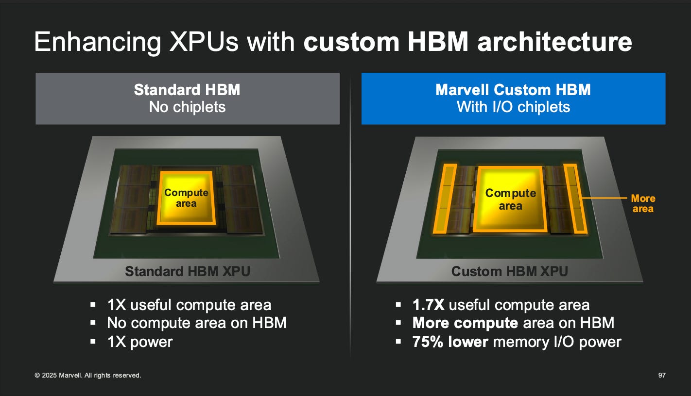
In parallel,Marvell’s customized HBM architecturefocuses on interface-level optimization by serializing and accelerating I/O channels between the XPU and the HBM base die. This results inup to 70% reduction in interface power consumption. Additionally, the optimized interface design frees up die area—up to 25%—which can be reallocated to integrate more HBM controller logic or support33% more HBM stacks.
According to Marvell’s presentation, when paired with adisaggregated I/O die, the custom HBM platform enables approximately1.7× greater effective compute areacompared to standard HBM implementations, while reducing memory I/O power by75%.
Collectively, these strategies—tight coupling ofSRAM and HBM with compute units, and offloading connectivity throughmodular I/O dies—significantly improve AI chip compute efficiency, reduce power consumption, and optimize die area utilization. These innovations position Marvell’s architecture as highly scalable and power-efficient for next-generation AI infrastructure.

Facing the Slowdown of Moore’s Law: Marvell’s Platform Strategy for Advanced Process and IP Readiness

Facing the Slowdown of Moore’s Law: Marvell’s Platform Strategy for Advanced Process and IP Readiness
As Moore’s Law continues to slow,Marvell has adopted a platform-based strategyto proactively position itself at the forefront of advanced process technologies and silicon IP development. In its2025 2nm platform launch, Marvell unveiled thefirst chip IPs built on TSMC’s 2nm process, including a next-generation3D stacked die-to-die interface.
This platform approach consolidates a comprehensive suite of bothestablished and emerging technology modules—includinghigh-speed SerDes, die-to-die interconnects, advanced packaging solutions, silicon photonics, custom HBM, embedded SRAM, and SoC-level interconnectssuch asPCIe Gen7—serving as the foundational building blocks for the development ofcustom AI accelerators, CPUs, network switches, and more.
Marvell previously launched itsindustry-leading 5nm data infrastructure platform in 2020, followed by the3nm platform in 2022, with first silicon delivered in 2023 and multiple products now in mass production. This platform model enablespre-validated IP blockson the latest process nodes (e.g., 3nm, 2nm), which customers canreadily embedinto their designs.
For example, Marvell was among the first to demonstratelong-reach SerDes and advanced interface technologies on the 3nm node in 2023. The latest2nm platform not only showcases high-speed 3D I/O, but also reserves room for future scaling paths, including16Å and 14Å process generations.
Through close collaboration with foundry partners such as TSMC, Marvellco-develops and validates IP modules in sync with each process shrink, accelerating time-to-market for downstream SoC customers and improving compatibility across multiple technology generations.
In summary, Marvell’s strategy centers onpre-validating modular IPand developingmulti-generational SoC platforms, combiningprocess leadership with packaging innovationto meet the system design challenges of the2nm and Ångström-class era.


PreviousNext
TopLatestDiscussions








See all