Perspective on SerDes and CPO: PCB Material and Signal Routing Challenges Ahead
Perspective on SerDes and CPO: PCB Material and Signal Routing Challenges Ahead
- Source: SemiVision
- Author: SEMIVISION
- Published: 2025-07-08T21:10:30+08:00
- URL: https://tspasemiconductor.substack.com/p/perspective-on-serdes-and-cpo-pcb Perspective on SerDes and CPO: PCB Material and Signal Routing Challenges Ahead


Perspective on SerDes and CPO: PCB Material and Signal Routing Challenges Ahead
Original Article by SemiVision Research (TPCA Taiwan , TCPA Japan , EMC , Nvidia , Broadcom , Marvell , TSMC)

Jul 08, 2025
∙ Paid
How Will Material Innovation Become the Core Breakthrough for AI Infrastructure as SerDes Advances to 224G?
The AI server and high-performance computing (HPC) sectors are entering an era of unprecedented I/O density and bandwidth requirements. At the heart of this evolution lies the SerDes (Serializer/Deserializer) interface. From the early 28Gbps NRZ and 56Gbps PAM4 to today’s 112Gbps and soon-to-be-commercialized 224Gbps SerDes, each leap in bandwidth has relied not only on IC design improvements but also on a deeper, more complex challenge: materials innovation. At ultra-high frequencies, maintaining signal integrity, controlling insertion loss, and ensuring reliability amid thermal and mechanical stress all depend heavily on advanced substrate materials.
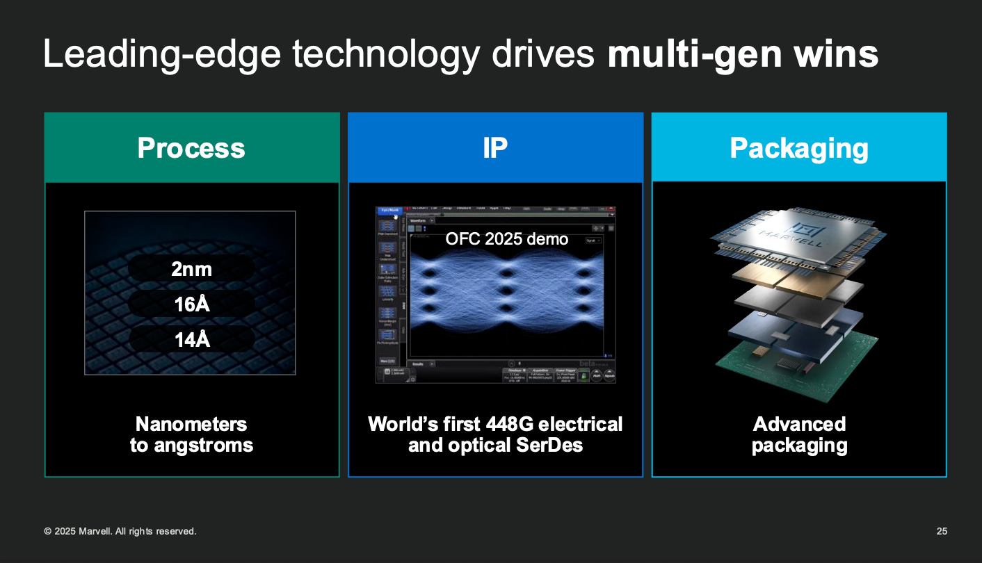
As generative AI and large language models evolve at an unprecedented pace, data center interconnect architectures are facing critical new challenges. With model sizes expanding into the hundreds of billions—and even trillions—of parameters, bandwidth bottlenecks and energy efficiency have become key constraints on scalable AI compute infrastructure. Marvell, a global leader in data infrastructure semiconductors, is redefining the interconnect paradigm for the AI era through its deep expertise in high-speed SerDes IP and silicon photonics technologies.
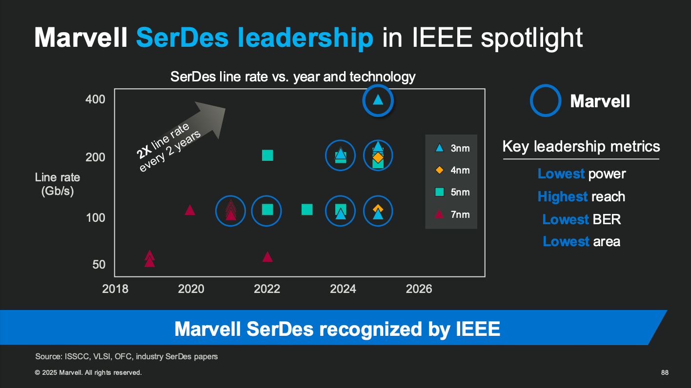
Since 2018, Marvell has led the industry in SerDes development, culminating in the demonstration of its 3nm, 224Gbps SerDes at OFC 2025. With innovations including optical retimers and gearboxes, Marvell is pushing toward 400+ Gbps per lane performance. These advancements demonstrate industry-leading metrics in ultra-low power (<0.1 pJ/bit), ultra-high bandwidth density (50+ Tbps/mm), and lowest bit error rates (BER)—solidifying its critical role in Co-Packaged Optics (CPO) and Die-to-Die (D2D) interconnect applications.
But Marvell’s strategy goes far beyond link-level IP. Its comprehensive IP portfolio spans SerDes, silicon photonics, dense SRAM, custom HBM, and advanced packaging—aligned with TSMC’s CoWoS platform and JEDEC standards. This enables scalable XPU and XPU attach solutions that support custom AI accelerators and heterogeneous deployment models across cloud and enterprise.

On the optical interconnect front, Marvell’s silicon photonics platform has seen multiple generations of field deployment—from 100G and 400G modules to the upcoming 1.6T solutions targeted for commercialization in 2026. By integrating photonics and electronics on a single silicon system and deploying 3D light engines on the package’s reverse side, Marvell’s CPO solutions offer up to 6.4Tbps per engine and 25.6Tbps in multi-engine configurations—providing essential scalability for data centers.
As SerDes and optical links move from board edges into chip cores, Marvell stands among the few full-stack providers capable of integrating electrical, optical, packaging, and software domains. Marvell’s IP leadership and co-design capabilities position it at the forefront of next-generation custom infrastructure and high-speed interconnect ecosystems.

In this wave of technological disruption, Taiwan-based Elite Material Co., Ltd. (EMC) has emerged as a key global driver of high-speed material innovation. Starting with halogen-free green HDI materials, EMC has now expanded its portfolio to cover next-generation packaging technologies such as AI servers, Co-Packaged Optics (CPO), Near-Package Optics (NPO), FCBGA, and Antenna-in-Package (AiP). EMC’s strategy demonstrates its remarkable transition from low-frequency mobile devices to ultra-high-speed, mission-critical infrastructure — from smartphones to space.
As AI servers compress transmission distances and signal edges become more fragile, the dissipation factor (Df) and coefficient of thermal expansion (CTE) are becoming critical indicators of material suitability. At 112Gbps PAM4 (~28GHz), traditional FR-4 or standard HDI materials are already stretched to their limits. With 224Gbps PAM4 pushing operating frequencies to ~56GHz, SerDes design now intersects with materials science, packaging architecture, and signal integrity engineering.
EMC has achieved a major breakthrough at this critical juncture. Its low-Df material EM-S532K features a Df of just 0.0037 — a substantial improvement over the previous-generation EM-S526 (Df 0.0081), reducing insertion loss by over 35% at 80GHz. To meet the demands of CPO architectures, where silicon photonics and electrical components are tightly co-packaged, EMC has also introduced materials such as EM-S570K3 and EM-S572T, featuring ultra-low CTE (<2 ppm/°C) and high modulus (>35 GPa) — essential properties for precise mechanical matching and long-term reliability in SerDes + SiPh integration.
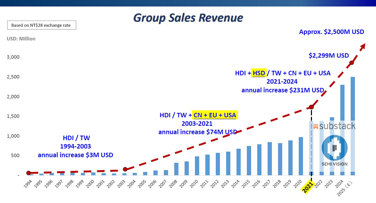
This wave of materials innovation is also reflected in EMC’s business trajectory. From the first materials boom triggered by smartphones in 2003, to the current transformation driven by AI servers since 2021, EMC’s annual revenue growth has jumped from $74 million per year to over $230 million annually. The company’s total revenue is projected to reach $2.5 billion in 2025, underscoring the explosive demand for next-generation high-speed substrates.

Global Demand for High-End CCL Surges Rapidly
With the rise of high-speed computing and communication applications, the global copper-clad laminate (CCL) market is undergoing a structural shift. While growth in the traditional mid-to-low-end FR-4 segment is slowing, demand for high-frequency, high-speed advanced CCLs is increasing significantly.
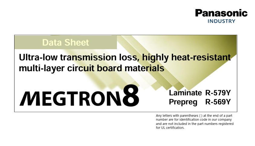
In particular, the advent of AI servers in cloud data centers and the transition to 800G network switches has driven many manufacturers to adopt ultra-low-loss materials like M8-grade CCLs (e.g., Panasonic Megtron 8). Launched in 2022, Panasonic’s Megtron 8 supports 800GbE high-speed networks and features a dielectric loss factor (Df) of approximately 0.0015—about 25% lower transmission loss compared to the previous-generation Megtron 7 (Df ≈ 0.002).
These M8+ high-performance materials, known for their low dielectric constant and minimal signal loss, are becoming essential for next-generation high-speed PCB designs. According to a CCL industry report released by Goldman Sachs on November 20, 2024, the global high-end CCL market is projected to achieve a compound annual growth rate (CAGR) of 26% from 2024 to 2026—significantly outpacing the overall CCL market’s growth rate of around 9%.
Regional Market Development:
The supply of high-end CCLs is primarily concentrated in Asia, particularly in Taiwan, South Korea, and Japan. While Chinese manufacturers hold a strong position in the mid-to-low-end CCL market, they still lag behind in both technology and certification when it comes to ultra-high-frequency M8-grade materials. As a result, this segment is currently dominated by suppliers from Taiwan, Korea, and Japan.
Due to ongoing U.S.-China tech tensions, American tech giants increasingly rely on supply chains based in Taiwan, Korea, and Japan for their AI servers and high-speed network switches. This shift has driven up shipments of high-end CCLs from Taiwanese manufacturers. Key players in the M8-generation supply chain include Taiwan's EMC, TUC and Iteq, South Korea’s Doosan, and Japan’s Panasonic, forming the core competitive group in the current high-end CCL market.

When SerDes Advances to 224G, How Does Materials Innovation Become the Core Breakthrough of AI Infrastructure?
Today’s AI servers and high-performance computing (HPC) systems are facing unprecedented demands for I/O density and bandwidth. One of the key enabling technologies behind this shift is the SerDes (Serializer/Deserializer) interface. From early 28Gbps NRZ and 56Gbps PAM4 to 112Gbps and now the emerging 224Gbps SerDes, each leap in bandwidth isn’t just about IC design—it critically depends on materials innovation. Maintaining signal integrity, managing insertion loss, and enduring mechanical stress under high-frequency conditions all require advanced substrate materials.
Amid this wave of technological change, Taiwan-based Elite Material Co., Ltd. (EMC) has emerged as a global leader in high-speed base materials. Originally known for its halogen-free HDI materials, EMC has now extended its product coverage to support emerging advanced packaging architectures including AI servers, Co-Packaged Optics (CPO), Near-Package Optics (NPO), FCBGA, and Antenna-in-Package (AiP). This showcases EMC’s broad technical range—from mobile to aerospace applications—and its strategic transformation.

For AI servers employing SerDes, shorter transmission distances and fragile signal edges make Df (Dissipation Factor) and CTE (Coefficient of Thermal Expansion) the key material metrics. At 112Gbps PAM4 (~28GHz), traditional FR-4 and HDI materials already struggle. With 224Gbps PAM4 pushing frequencies to 56GHz, SerDes becomes a multidisciplinary challenge involving materials science, packaging, and signal engineering.
EMC has achieved breakthroughs with materials like EM-S532K, reducing Df to 0.0037 (compared to EM-S526’s 0.0081), cutting insertion loss by over 35% at 80GHz. For CPO systems requiring photonic-electronic co-packaging, new materials like EM-S570K3 and EM-S572T feature ultra-low CTE (<2 ppm/°C) and high modulus (>35 GPa), supporting precise alignment and reliability.
This materials revolution is reflected in EMC’s revenue trajectory—from a $74M annual growth rate during the smartphone boom of the 2000s to over $230M per year since the AI server boom in 2021, with total revenue projected to reach $2.5B by 2025.
According to Prismark's 2023 report, EMC has become the world’s No.1 in the high-speed substrate market with a 28% share, surpassing Japan’s Panasonic and Taiwan’s TUC. EMC is also expanding in high-reliability sectors such as AI servers, network switches, LEO satellites, ADAS, and defense electronics.
More importantly, EMC is not only improving core material performance but also enhancing integration capabilities with advanced packaging. For example, the EM-S532K series for AiP improves high-frequency insertion loss and mitigates thermal stress caused by structural asymmetries in packaging due to its low CTE. This allows HDI-based materials to compete with fan-out and even glass interposer platforms in 5G/Wi-Fi 7 modules—offering a high-performance, scalable, and cost-effective solution.
In this context, materials are no longer passive enablers but strategic drivers of AI and high-speed architecture innovation. From SerDes specs to packaging and yield management, EMC embodies a "materials-driven architecture transformation" approach—cementing Taiwan’s role in the global high-frequency materials landscape.
Looking ahead, as CPO enters production and 1.6TbE and ultra-high-speed switches become mainstream, SerDes and silicon photonics will push materials science to new frontiers. Leaders like EMC, with systemic design thinking across Df, CTE, modulus, and packaging compatibility, will become the invisible core enabling next-gen data centers, EVs, satellite communications, and AI chips. This is not just a market opportunity—it is a redefinition of industry positioning.
This article will integrate PCB-level perspectives on SerDes design and explore key challenges in signal integrity (SI) and power integrity (PI). It will also provide a holistic view of electromagnetic compatibility -driven layout strategies. Our goal is to explain why AI chip system design is no longer just a chip-level issue — it also requires deep consideration of PCB architecture, materials, and system-level interactions.
Furthermore, the article will deliver a comprehensive analysis that bridges chip, board, and material layers, with updated insights into high-speed transmission strategies currently being adopted by companies like Broadcom and Marvell.

2025年7月6日
For Paid Members ,SemiVision will discuss topics on
What is CCL?
SerDes Bandwidth Evolution and Its Systemic Implications in the AI and Silicon Photonics Era
Comprehensive Understanding of Impedance Matching and Loss Budgeting: The Core Battlefield of Signal Integrity in the High-Speed Design Era
Power Integrity (PI) First: The Foundation of System Reliability
SI Comes Next: Precision in Impedance and Loss Budget
The Design Loop: From PI to SI to Material Strategy
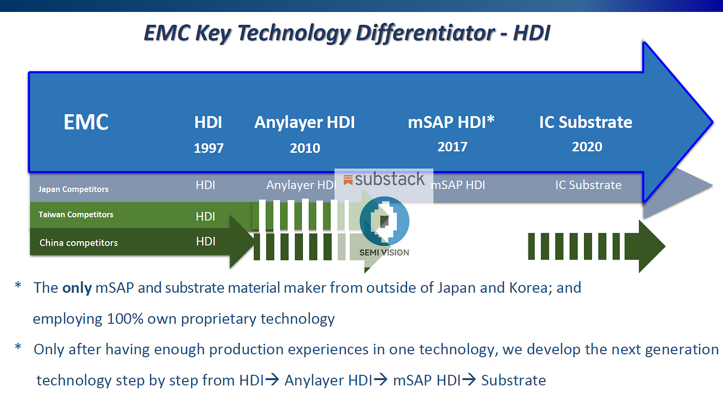
EMC Group Sales Growth – From Foundation to Acceleration
EMC Global Ranking in 2023 – Market Leadership in HDI and Halogen-Free Laminates
EMC – Global No.1 in High-Speed Laminate (2023)
EMC Product Roadmap for FCBGA/SiP
What is AiP?
Key Industry Trends Reflected in the Image in AiP
Key Advantages of EMC’s HDI-Based Solutions
Chart Analysis: Insertion Loss vs. Frequency
Five Generations of Optical Module Evolution (2022–beyond)
Silicon Photonics (SiPh): The Key Enabler
Mega Trend in Optical Module material viewpoints from EMC
High-Speed SerDes and Optical Interconnect Trends
What is CCL?
Copper-Clad Laminate (CCL) is a core material used in the fabrication of printed circuit boards (PCBs). It consists of a non-conductive insulating substrate (usually made of epoxy resin + glass fiber) laminated on one or both sides with a thin layer of copper foil.

Structure of CCL:
Core: Insulating base (e.g., FR-4, BT resin, PI film, etc.)
Copper Foil: Laminated on one or both sides
Optional Enhancements: Fillers, halogen-free resins, or low-Df dielectric materials for high-frequency applications

Function of CCL:
Supports electrical circuitry— Acts as the skeleton of a PCB.
Provides mechanical strength— Ensures rigidity and heat resistance.
Enables high-frequency signal transmission— Through low Dk/Df material formulation.
Acts as thermal management interface— Important for high-speed, high-power devices.

SerDes Bandwidth Evolution and Its Systemic Implications in the AI and Silicon Photonics Era
As silicon photonics and AI chip architectures continue to evolve, the breakthrough in SerDes (Serializer/Deserializer) bandwidth has become one of the core driving forces behind overall system performance. The transition from 112G to 224G, and now to 448G, not only represents a doubling of data rates, but also highlights the physical design limits of traditional electrical interconnects. The arrival of 448G SerDes, in particular, signals the growing challenge for copper routing, silicon interconnects, and signal integrity (SI) engineering.
Among global suppliers, Broadcom stands as the sole vendor to have commercially deployed 448G SerDes chips, positioning itself as the leading player for this next-generation high-speed interface. While Marvell and MediaTek currently concentrate on 112G–224G SerDes technologies, both are actively advancing higher-speed platform roadmaps and verification efforts. This indicates that 448G SerDes is no longer a theoretical concept—it’s becoming a practical necessity for future AI infrastructure.
Importantly, the competitive landscape is no longer limited to SerDes IP design capabilities. Both Broadcom and Marvell are pursuing full-stack co-design strategies that integrate silicon photonics platforms, optical engines, and co-packaged optics (CPO). Broadcom’s AI switch architecture integrates on-die silicon photonic transceivers to shorten signal paths and reduce power loss. Marvell, leveraging its in-house photonics engines and packaging technologies, is commercializing 51.2Tbps-class switching platforms. These developments not only enable higher bandwidth density, but also drastically improve power efficiency, latency performance, and system resiliency through advanced photonic-electronic integration.
However, as channel rates rise to 224G and 448G, the energy and thermal density per bit sharply increases. This narrows the design margin for PI/SI across the entire signal path—from ASIC, to packaging, substrates, and connectors. At these frequencies, even minor discontinuities in traces, vias, or connectors—such as impedance mismatches, crosstalk, or insertion loss—can cause serious bit error rate (BER) issues. Thermal-induced degradation in Df (dissipation factor) and copper loss further complicates the challenge. Traditional mid-range PCB materials like FR-4 or M6 are no longer sufficient for such designs.
To meet stringent PI/SI requirements at high frequencies, materials with high Tg, low Dk/Df, and strong thermal stability have become a structural necessity. One of the current mainstream solutions is Panasonic's Megtron 8 (M8), which maintains extremely low insertion loss and impedance stability in the 14–28 GHz range. M8 is widely adopted in 224G SerDes system boards and optical module substrates. Looking ahead, Megtron 9 (M9) is expected to further improve CTE (coefficient of thermal expansion) and conductor compatibility, supporting more demanding reflow environments, and addressing thermal stress and reliability issues in CPO and OIO (Optical I/O) environments.
In summary, SerDes scaling is no longer just about PHY IP advancement—it has become a system-level engineering challenge that spans packaging, interconnects, materials, and photonic integration. This article follows the trajectory from 112G → 224G → 448G, analyzing the platform strategies of Broadcom and Marvell across SerDes, silicon photonics, optical interconnects, and packaging.
We will further explore why thermal budgets, PI/SI simulation, and especially next-gen PCB materials (M8/M9) are no longer peripheral considerations, but rather the critical enablers determining whether next-generation designs can transition from lab to deployment.
Comprehensive Understanding of Impedance Matching and Loss Budgeting: The Core Battlefield of Signal Integrity in the High-Speed Design Era
As chip performance continues to advance and system complexity escalates, signal integrity (SI) has evolved from a secondary concern into a critical determinant of success in high-speed communication and packaging integration. Against the backdrop of increasingly frequent adoption of data centers, AI accelerators, GPU clusters, and silicon photonics, precise impedance matching, loss budgeting, and thermal-electrical co-design have become inescapable challenges for circuit designers, package planners, and system integrators alike.
This article starts from the theory of impedance matching, incorporates the logic behind loss budget calculations in high-speed SerDes transmission, and further explores how material selection and PCB stack-up design significantly impact channel performance. We then extend the discussion to new SI challenges in Co-Packaged Optics (CPO) and 3D-integrated packaging, offering a systematic and practical technical perspective.
- Principles and Importance of Impedance Matching
The fundamental concept of impedance matching stems from the reflection phenomenon encountered when high-frequency signals propagate through different media. When the characteristic impedance of a transmission line does not match the source or load impedance, part of the signal reflects back to the source, resulting in waveform distortion, interference, and bit errors. In SerDes systems operating at 56G, 112G, or even 224G, any form of reflection or insertion loss can collapse the eye diagram, leading to elevated bit error rates (BER).
In modern high-speed design, common differential impedance targets are 85 Ω (e.g., PCIe) and 100 Ω (e.g., Ethernet, SerDes). Designers must ensure impedance variation across PCB traces, vias, connectors, and packaging segments is kept within ±10% — or preferably ±3%. Even a small 5Ω mismatch in a 112G PAM4 environment can cause significant signal reflections and increased jitter, threatening system stability.
- Design Logic Based on Loss Budgeting
Loss budgeting provides a quantitative framework for signal integrity planning. Designers must define an allowable total insertion loss (IL) across the entire channel and allocate it based on the transmission architecture and number of interconnects. For instance, in 56G PAM4 designs, many chip vendors recommend limiting total IL to 28 dB (at the Nyquist frequency). At 112G NRZ or 224G PAM4, total IL often needs to be constrained within 30–32 dB.
The loss budget should consider:
Insertion loss from PCB trace length and material properties
Impedance discontinuities and return loss from SMT connectors
Parasitic effects and coupling loss from vias and BGA balls
Return loss at pluggable modules and package interfaces
Engineers should use SI simulation tools (such as Sigrity, ADS, HFSS) to model each segment with S-parameters, evaluate total IL and return loss against chip vendor channel specifications, and validate eye diagrams, jitter, BER, and equalizer performance.
- Impact of PCB Materials and Core/PP Stack-Up on SI
Beyond trace layout, the choice of PCB material and stack-up design is critical for SI optimization. Materials such as FR4, M6, Megtron 7, and Panasonic R-5755 differ in dielectric constant (Dk) and dissipation factor (Df). At high frequencies, Df significantly affects insertion loss, with strong temperature dependence. For example, Df for M6 materials at 80°C may be 25% higher than at room temperature, increasing IL by over 1 dB.
Core and Prepreg (PP) layers in stack-ups influence impedance control and transmission loss. Core layers provide rigidity and fixed spacing, beneficial for consistent impedance. PP layers offer dielectric transition and mechanical adhesion, but their thickness variations can induce impedance discontinuities and process variability.
Design recommendations include:
Use low Df, high-frequency materials for SI-critical layers
Minimize trace-to-plane spacing; adopt 2W/3W spacing to control crosstalk
Prioritize differential pairs on symmetric routing layers in stack-up
Avoid excessive vias or plane cuts in high-speed signal paths
- New SI/PI Modeling Challenges under Thermal-Electrical Coupling
In the era of AI chips consuming hundreds of watts, conventional room-temperature SI/PI models are no longer reliable. High-power chips cause localized PCB heating, which significantly affects material properties such as copper conductivity, Df, and capacitor stability. Thermal-to-SI/PI coupling has thus become a new standard design requirement.
Thermal effects on SI include:
Decreased copper conductivity increases resistance and signal loss
Elevated Df in materials, especially in mid-tier laminates (e.g., M4), can raise IL by over 60%
Frequency response distortion impairs equalizer performance and simulation accuracy
For PI, higher DCR increases IR drop, while MLCCs may experience capacitance shifts or reductions by tens of percent at high temperatures, compromising PDN impedance and resonance behavior.
Advanced design flows should adopt temperature-aware simulations:
Perform thermal simulation using Cadence Celsius or Ansys Icepak
Feed temperature maps into SIwave, PowerSI, or PowerDC for coupled simulations
Maintain consistent thermal-reference points across layout and simulation data formats
- Impedance Design Challenges in the Era of CPO and Silicon Photonics
As the industry transitions into photonic packaging and CPO (Co-Packaged Optics), traditional electrical signaling must integrate with optical pathways. While photonic modules greatly reduce loss over long distances, internal packaging still relies on short, high-speed electrical channels from ASIC to photonic engines for E-O conversion — a domain still governed by SI constraints.
Impedance matching becomes more complex:
ASIC and photonic ICs are often connected via 3D integration or EMIB/interposer, requiring impedance compatibility between die pads and waveguide drivers
SiPh components like Mach–Zehnder modulators, micro-ring modulators, and Ge photodiodes exhibit different electrical models and load characteristics than traditional CMOS
Package-level traces may only span millimeters but operate at frequencies up to 56–112 GHz, making any impedance discontinuity critically impactful
Design solutions in this context should include:
Full 3D simulation models integrating electrical and optical domains
Multi-parameter sensitivity analysis across temperature, materials, and substrate thickness
Automated design tools for die-to-PIC interface optimization within advanced packaging environments
Impedance Matching Is Not Just Trace Design — It’s a System Design Philosophy
Signal integrity (SI) has never been merely about circuit simulation. It is a multidisciplinary engineering practice that spans materials science, structural mechanics, electromagnetics, thermal behavior, and advanced packaging processes. In today’s high-speed system design, impedance matching and loss budgeting have entered a new era—one that demands dynamic analysis, cross-domain verification, and iterative experimental modeling.
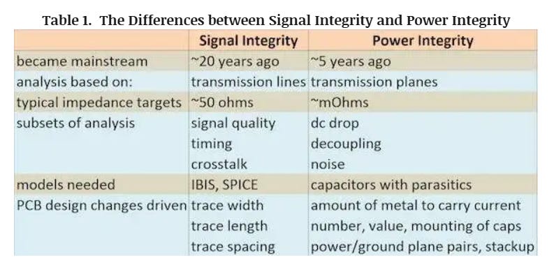
Source: EDN
From impedance and insertion loss, to PCB stackups and thermal-electrical coupling, every design decision must navigate a fine balance between performance, cost, and reliability. Success in the age of AI data centers, advanced packaging, Co-Packaged Optics (CPO), and System-on-Integrated-Chips (SoIC) hinges on developing a system-level mindset—one that connects material stackups directly to signal budgets.
Power Integrity (PI) First: The Foundation of System Reliability
In high-speed, high-power systems—especially AI accelerators and next-gen GPUs—power delivery network (PDN) design is foundational. Without stable power impedance and minimal IR drop, even perfectly optimized signal designs can lead to system instability due to voltage fluctuations.
Thermal effects such as MLCC capacitance derating, ESR increase, and DCR rise in conductors at elevated temperatures must be modeled using thermal-PI co-simulation tools (e.g.,Cadence PowerDC). Ensuring PDN stability under worst-case thermal scenarios (junction temperature ≥ 100°C) is essential to preserving downstream SI margins.
SI Comes Next: Precision in Impedance and Loss Budget
Once a robust PI network is established, SI simulation takes the lead. For 112G and 224G SerDes channels, impedance deviations must be controlled within ±3%, to prevent reflections, while insertion loss (IL) must remain within ~30 dB to avoid signal degradation, excessive jitter, and Bit Error Rate (BER) violations. These simulations depend heavily on accurate modeling of traces, vias, connectors, and stackup transitions.
However, when traditional FR-4 or entry-grade substrates are used, Dk/Df variability under high-frequency and high-temperature conditions results in large discrepancies between simulation and measurement, leading to reduced signal margins and even SI design failure.
The Materials Turn: When PI and SI Reveal the Need for Substrate Innovation

The Design Loop: From PI to SI to Material Strategy
This is not a linear sequence, but a closed-loop design cycle. If SI simulations indicate poor margins, the solution often lies not in rerouting, but in upgrading the substrate. Megtron 8 and 9, with their ultra-low-loss and high thermal reliability properties, align PI and SI simulation results, ensuring robust system performance under real-world stress.
In essence, material innovation becomes the decisive inflection point for next-generation high-speed, high-power, and high-frequency systems. Only with such a system-centric approach—from power integrity, to signal precision, to material science—can engineers confidently navigate the future of AI infrastructure and high-performance interconnects.

EMC Group Sales Growth – From Foundation to Acceleration
EMC, a Taiwan-based substrate materials manufacturer founded in 1992, initially focused on halogen-free materials for HDI (High-Density Interconnect) applications. In the early years, our revenue growth was modest, but over time, we have witnessed a significant and sustained upward trajectory—driven by two key inflection points:

EMC Product Roadmap for FCBGA/SiP
EMC's advanced material roadmap for FCBGA/SiP packaging, with a strategic focus on deliveringlow XY CTEandhigh modulussolutions—key enablers for next-generation high-density, high-performance semiconductor packages.
Key Observations and Trends:
Shift Toward Lower CTE & Higher Modulus:
As computing power increases and package complexity rises, warpage and thermal mismatch become critical challenges. The industry's direction is clearly moving toward materials with:
CTE < 1 ppm/°C, targeting extreme low thermal expansion
Modulus > 40 GPa, to support warpage control in large-area or multi-die integration
Product Roadmap:
EM-S526: A widely adopted MP (mass production) solution, used extensively in current SiP applications but with higher CTE (~9 ppm/°C).
EM-S570: Combines high modulus and reduced CTE (~5 ppm/°C), well-suited for flip-chip and SiP formats in mass production.
EM-S572T (Q4’25)andEM-S570K3 (Q3’25): New materials under development that push further toward the ideal performance zone—extremely low CTE (<2 ppm/°C)withhigh modulus (>35 GPa). These are tailored for emerging FCBGA/SiP needs in AI, HPC, and edge applications.
EM-S570T: Currently a sample stage product balancing performance for advanced development and qualification.

EMC is clearly positioning itself as a materials innovator in the advanced packaging space. With the upcoming EM-S570K3 and EM-S572T, EMC is targeting the"Extreme XY CTE + High Modulus"zone—essential for enabling the next wave of SiP, HPC, and AI packages that demand dimensional stability, high I/O density, and mechanical robustness.
This aligns with broader industry trends toward glass-core substrates, heterogeneous integration, and AI-centric architectures, where material science plays a pivotal role in system reliability and yield.

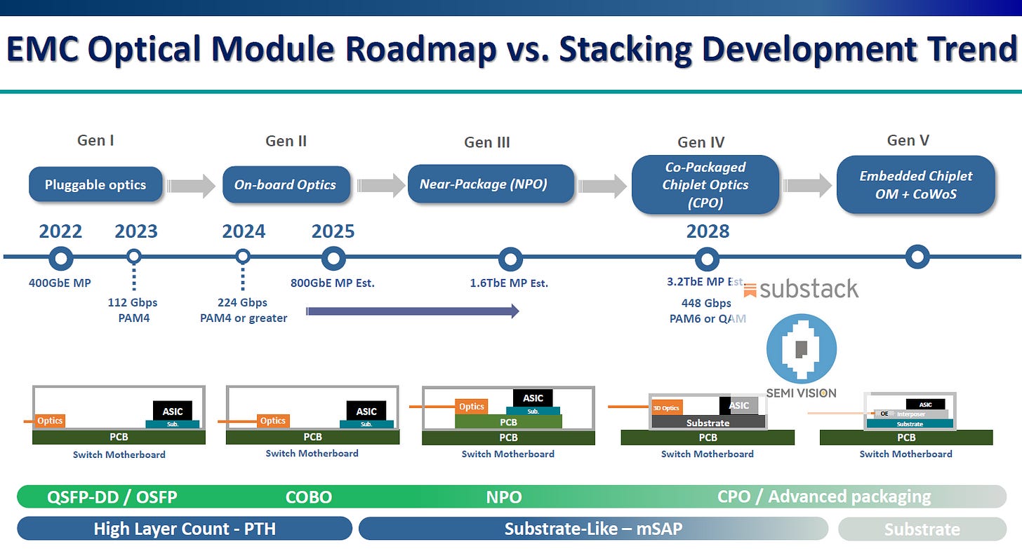
Five Generations of Optical Module Evolution (2022–beyond)
EMC Optical Module Roadmap alongside key stacking and packaging technology trends, illustrating the industry's transition toward higher bandwidth density, lower power, and tighter integration—a direction strongly aligned with the rise of silicon photonics (SiPh).
Gen I: Pluggable Optics (2022–2023)
Modules likeQSFP-DD / OSFPusing400GbE, scaling to112 Gbps PAM4.
Optics and ASICs placedseparately on PCB, with traditional high-layer count substrate (PTH).
Still dominant, but reaching limits in power, latency, and signal integrity.
Gen II: On-board Optics (2024)
Optical engines movecloser to ASIC, reducing interconnect length and improving performance.
224 Gbps PAM4 or higherbecomes the norm.
COBO (Consortium for On-Board Optics) specifications adopted.
Gen III: Near-Package Optics (NPO) (2025)
Optics now integrated near the substrate withsubstrate-like PCB (mSAP).
Prepares for1.6TbEdeployment.
Start of closer photonic-electronic coupling, increasing feasibility for silicon photonics integration.
Gen IV: Co-Packaged Optics (CPO) (2028)
Marks the shift totrue co-packaging: optics and ASICs integrated on thesame substrate.
Enables448 GbpsPAM6 or QAM modulation.
Requires3D optics integration, low-CTE high-performance substrate, and thermal innovation.
Major milestone for silicon photonics—SiPh engines are now directly integrated at package level.
Gen V: Embedded Chiplet Optics + CoWoS (Beyond 2028)
Fully embeddedchiplet optical modules, leveragingTSMC CoWoSor similar advanced packaging.
Enables high-speed, energy-efficient interconnects across chiplets and optical I/O.
SiPh becomes astandard building blockinside data center and AI accelerators.
Silicon Photonics (SiPh): The Key Enabler
As speed scales from 112G → 224G → 448G per lane,electrical interconnects become a bottleneck. Silicon photonics provides:
High-bandwidth, low-loss optical interconnects
CMOS-compatible integrationfor co-packaging with logic
Thermal and power advantagesas density increases
Gen IV and Gen V designs make SiPh-based CPO the centerpiece of next-generation optical modules, enabling hyperscale data centers and AI systems to meet their I/O demands.
Substrate & Packaging Trend
The roadmap moves fromtraditional PCBs with through-hole vias (PTH)tomSAPand ultimatelyadvanced 2.5D/3D substrates.
EMC’s positioning insubstrate innovation(e.g., low CTE, high modulus, optical alignment structures) is crucial for enabling reliable, low-loss optical-electronic integration.
This roadmap shows a clear convergence between optical module evolution, packaging advancement, and silicon photonics adoption. EMC's substrate technologies—spanning high-density interconnects, co-packaging platforms, and future CoWoS-compatible materials—form the foundation of this optical-electronic transformation.
Silicon photonics is no longer an R&D concept—it’s a packaging challenge, and EMC is helping solve it.
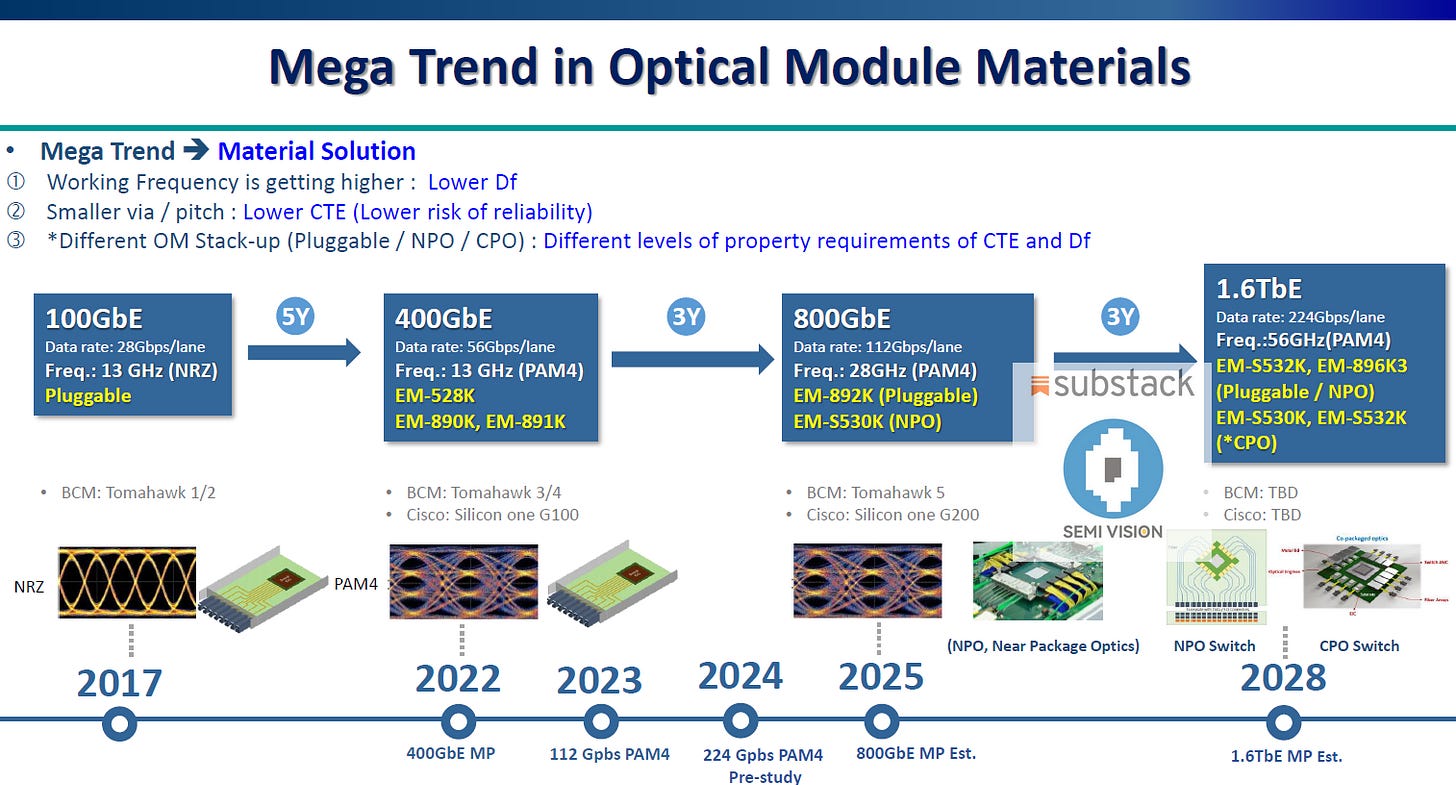
Mega Trend in Optical Module material viewpoints from EMC
The roadmap from 100GbE (2017) to 1.6TbE (2028) clearly reflects amega trendin bothelectrical performanceandmaterial innovation.
Bandwidth Leap and Frequency Surge
In just over a decade, data rates have grown from 28Gbps/lane to 224Gbps/lane, while operating frequency has surged from 13GHz (NRZ) to 56GHz (PAM4).
This dramatic shift introduces serious challenges in signal loss, latency, and reliability—placing unprecedented demands on optical module materials.
Material Challenges & Solutions
Three key material performance parameters now dominate optical module design:
Df (Dissipation Factor): Lower Df is essential to minimize insertion loss at high frequencies.
CTE (Coefficient of Thermal Expansion): Lower CTE reduces mechanical stress and improves reliability, especially asvia and pitch dimensions shrink.
Compatibility with different stacking architectures: Pluggable, NPO (Near-Package Optics), and CPO (Co-Packaged Optics) each have distinct material needs, especially at high-speed interconnects.
By 2028, the industry is expected to transition toward CPO (Co-Packaged Optics), a key enabler for 1.6TbE and beyond. In this architecture:
Optics and ASIC are co-integrated at the substrate level.
Power, heat, and signal integrity are tightly managed.
EMC’s new materials like EM-S532K are specifically designed to meet the extreme demands of CPO—balancing thermal, mechanical, and RF performance.
The mega trend in optical modules isn’t just about speed—it’s a materials arms race. As line rates double every 3–5 years, next-generation materials like EMC's ultra-low Df and low-CTE laminates are becoming mission-critical. EMC’s portfolio positions it as a leading enabler of the next wave of high-speed optical interconnects, from pluggable to chiplet-level photonics.
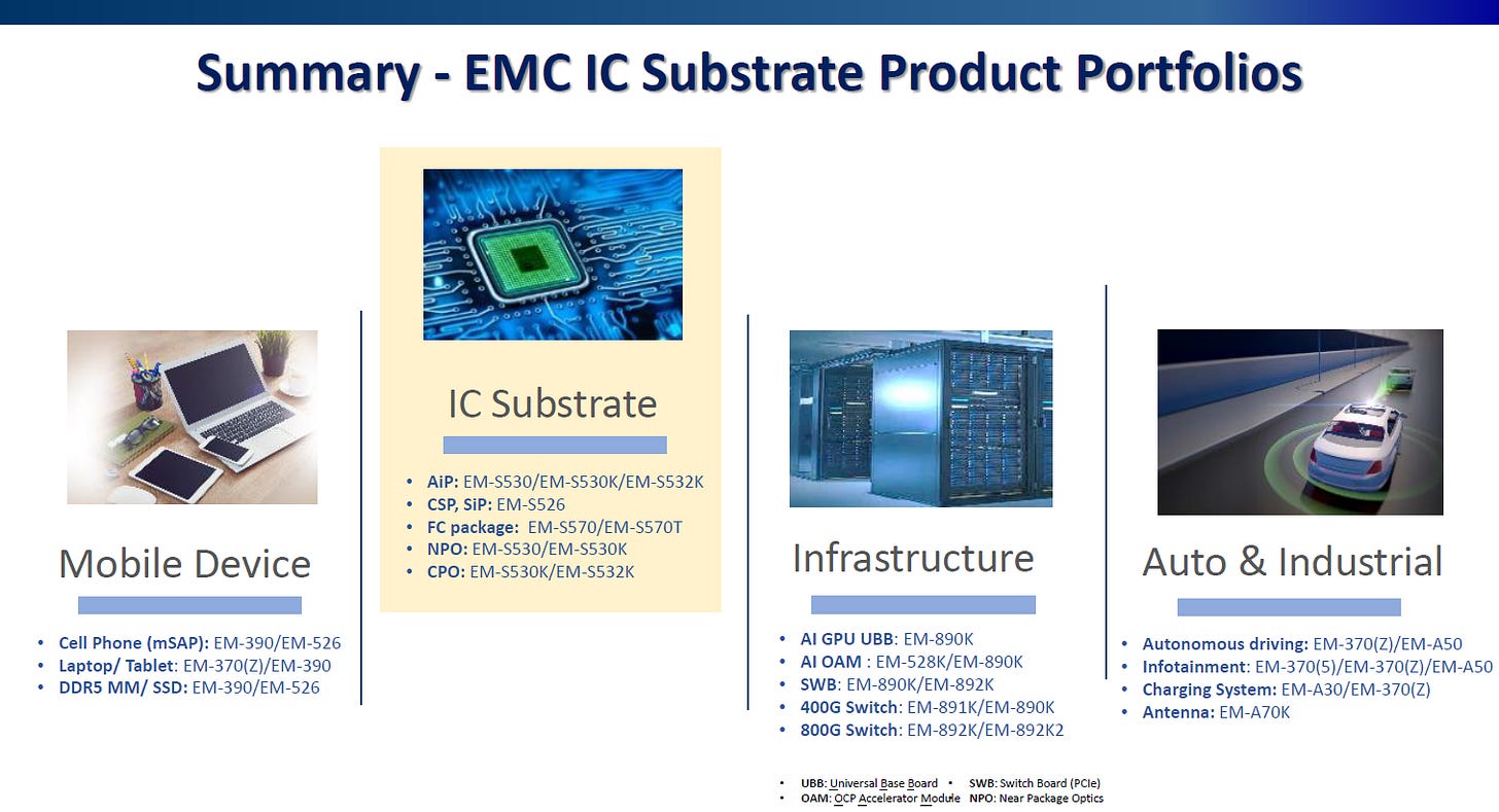
The summary slide provides a comprehensive overview of EMC's IC substrate product portfolio, showcasing its broad application across three major sectors: Mobile Devices, Infrastructure, and Automotive & Industrial. Each segment is supported by a targeted lineup of EMC materials engineered to meet performance, form factor, and integration requirements in next-generation electronics.
Mobile Devices
EMC supports the ultra-thin, high-density needs of smartphones, tablets, and laptops through itsmSAP-compatiblesubstrate materials. Key highlights include:
EM-390 / EM-526for cell phones using modified semi-additive processing.
EM-370(Z) / EM-390optimized for compact laptops and tablets.
EM-390 / EM-526also applied inDDR5 memory modules and SSDs, where signal integrity is critical.
Infrastructure / Data Center
With the rapid expansion of AI workloads and hyperscale data centers, EMC offers a range of high-performance substrate solutions for:
AI GPUsandOAMsusingEM-890KandEM-528K, enabling high power and high speed.
Switch Boards (SWB)such as 400G/800G optical switches, supported byEM-891K, EM-892K.
Near-Package Optics (NPO)andCPOintegration, where low Df and low CTE materials likeEM-S530K / EM-S532Kare essential.
Automotive & Industrial
For future vehicles and industrial automation, EMC offers substrates optimized for:
Autonomous driving ECUsusingEM-370(Z)andEM-A50.
Infotainment systems, where thermal and signal demands are balanced withEM-370(5)andEM-A50.
Charging modulesandantenna units, served byEM-A30andEM-A70K.
Core IC Substrate Applications
EMC’s product lines are tailored to key advanced packaging types:
AiP (Antenna-in-Package): EM-S530, EM-S530K, EM-S532K
CSP / SiP: EM-S526
FC BGA: EM-S570, EM-S570T
NPO / CPO: EM-S530K, EM-S532K
EMC's substrate technologies span across the full electronics spectrum—from ultra-compact mobile devices to AI data infrastructure and automotive intelligence. With a deep focus on low Df, low CTE, high modulus, and integration-ready platforms, EMC is positioned as a core enabler of the next wave of performance-driven and miniaturized systems.
High-Speed SerDes and Optical Interconnect Trends
Evolution and Limits of SerDes Interfaces:
As SerDes data rates continue to double—from 112G to 224G and eventually to 448G—both transmission speed and energy density are rising, imposing stricter requirements on PCB transmission channels, including length, impedance matching, and insertion loss. Industry reports indicate that 102.4Tbps ASICs using 112G/224G SerDes are already pushing the limits of traditional PCB routing. The move to 448G will introduce even more complex design challenges. Key issues for discussion include the physical limits faced by electrical channels at high frequencies—such as trace reflections, via-induced interference, and trade-offs between signal quality and power consumption.
The Role of Silicon Photonics and Co-Packaged Optics (CPO):

2025年6月4日
Platform Strategy Comparison – Broadcom vs. Marvell/MediaTek:
Broadcom has led the commercialization of 224G SerDes, deploying 112G/224G lanes in its 102.4Tbps switching chips, with its next-generation platforms targeting 448G. In contrast, Marvell and MediaTek currently focus on 112G–224G solutions, but are actively developing higher-spec technologies. MediaTek has officially stated that its 224G SerDes is ready for mass production and that it is "aggressively developing 448G SerDes" to meet future demands. The discussion can explore differences in IP design, optical integration, and packaging strategies among these leading vendors.
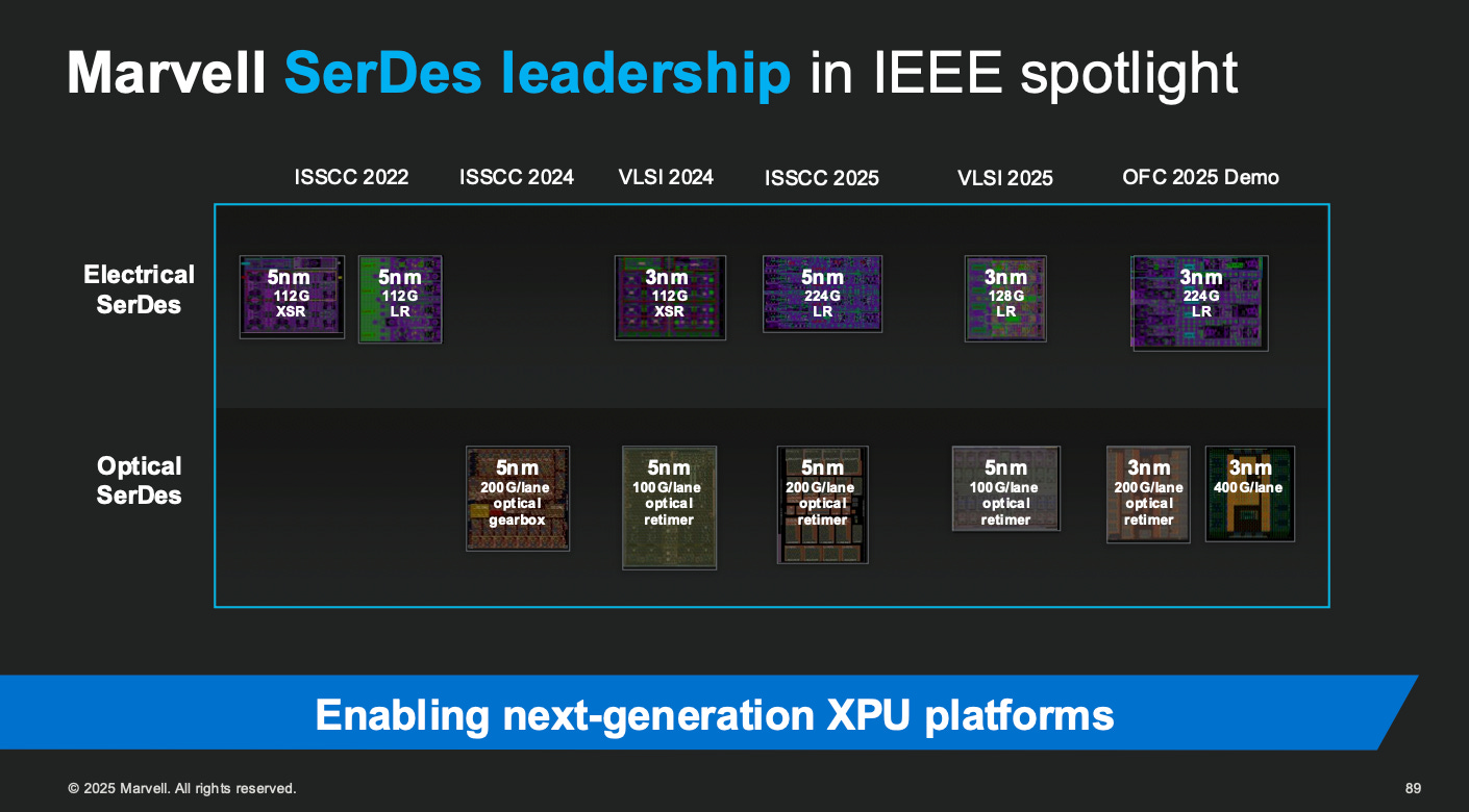
System-Level Co-Design and Bandwidth Density:
The evolution of SerDes has surpassed standalone channel design and now requires holistic chip-module-system integration. Broadcom has embedded silicon photonic transceivers into its AI switch architecture, drastically reducing power by shortening electrical paths. Marvell, leveraging its proprietary photonic engine and advanced packaging, has developed a 51.2Tbps platform. These co-design strategies aim to maximize bandwidth density while improving energy efficiency and system robustness—critical factors worth emphasizing.
SI/PI and Thermal Management Challenges at High Speeds:
At 224G and 448G, energy and thermal density per bit increase dramatically, significantly reducing the tolerance for power integrity (PI) and signal integrity (SI) along the transmission path. Even minor trace discontinuities, insertion loss, or crosstalk can lead to severe bit error rate (BER) issues. Thus, key discussion points include how to analyze and optimize thermal budgets and SI/PI simulations in design, and how to address increased signal loss in traditional FR-4 materials under high frequencies.
To meet the high SI/PI demands of ultra-high-speed transmission, materials with high Tg and low Dk/Df are essential. Panasonic Megtron 8 is a leading solution, optimized for networking equipment and offering roughly 30% lower insertion loss in the 14–28GHz range compared to previous generations, making it suitable for 800GbE and similar high-frequency applications. Megtron 8 is now widely used in 224G SerDes system boards and optical module substrates. Looking ahead, Megtron 9 is expected to further improve CTE and conductor compatibility, enhancing thermal stress resistance and reliability in CPO/OIO packaging environments.

AI Infrastructure Interconnect Standards and Future Trends:
In addition to the technologies mentioned above, the industry is paying close attention to other emerging interconnect standards and protocols. Examples include UCIe and PCIe Gen7—as highlighted by MediaTek—as well as advanced optical interconnect platforms , which may evolve alongside SerDes and CPO technologies. These developments are expected to become key topics in next-generation AI system design, particularly in addressing how to achieve higher-density internal channel interconnects while balancing energy efficiency, cost, and compatibility. Furthermore, optimizing the trade-offs between performance and cost across these new interfaces will be an important area for future exploration.


PreviousNext
TopLatestDiscussions








See all