EMC: From Copper to Light - Advanced CCL Solutions for Photonic Packaging
EMC: From Copper to Light - Advanced CCL Solutions for Photonic Packaging
- Source: SemiVision
- Author: SEMIVISION
- Published: 2025-07-06T00:45:26+08:00
- URL: https://tspasemiconductor.substack.com/p/emc-from-copper-to-light-advanced EMC: From Copper to Light - Advanced CCL Solutions for Photonic Packaging


EMC: From Copper to Light - Advanced CCL Solutions for Photonic Packaging
Original Article by SemiVision Research (TPCA Taiwan, JPCA, IMPACT, EMC, NVIDIA, TSMC)

Jul 06, 2025
∙ Paid

Hosted byTPCAand TPCA Japan, today’sKumamoto Taiwan High‑Tech Forumon June 10, 2025 brought together industry leaders includingTSMC , SPIL, Unimicron, Elite Material Co., Ltd. , Nanya, Eternal and CSUN. Through a series of in‑depth keynote presentations, panel discussions, and technical exchanges, the forum spotlighted Kumamoto’s strategic rise as a vital hub in the Taiwan‑Japan semiconductor value chain—setting the stage for new partnerships in high‑tech manufacturing and material innovation.

The TPCA Taiwan-Japan Tech Forum has provided updated insights into the latest industry developments.

2025年6月11日

IMPACT Introduction: Since its inception in 2006, the IMPACT Conference has been at the forefront of technological evolution, fostering innovation in the packaging, PCB, and semiconductor industries. Over the past two decades, IMPACT has not only witnessed but actively contributed to rapid advancements in 5G, AI, high-performance computing (HPC), edge computing, and sustainability. Each year, the conference has adapted to the latest trends, driving forward the conversation on emerging technologies and their industrial applications.
Now in its 20th year, IMPACT 2025 embraces the theme “Energy-Efficient AI: From Cloud to the Edge,” reflecting the industry’s growing emphasis on high-performance, low-power solutions. As AI applications continue to expand—from data centers to edge devices—the need for advanced PCB, IC substrates, heterogeneous integration, and packaging technologies has become increasingly critical.
This milestone year marks not just a celebration of the past 20 years, but a bold step into the future, where IMPACT continues to lead, inspire, and drive innovation. Join us at IMPACT 2025 as we shape the next era of AI, semiconductor packaging, and PCB technology—powering a smarter, more sustainable world.
【Date】Oct. 21st(Tue.)-24th(Fri), 2025
【Venue】Taipei Nangang Exhibition Center
【Theme】Energy efficient AI: From Cloud to the Edge
【Organizer】IEEE-EPS, iMAPS Taiwan, ITRI, TPCA
【Feature】Plenary speech, Industrial session, Special session, Invited talks, PDC
【Exhibition】TPCA Show, TAITRONICS, AIoT Taiwan
【On-line Submission】www.impact.org.tw
Global Demand for High-End CCL Surges Rapidly
With the rise of high-speed computing and communication applications, the global copper-clad laminate (CCL) market is undergoing a structural shift. While growth in the traditional mid-to-low-end FR-4 segment is slowing, demand for high-frequency, high-speed advanced CCLs is increasing significantly.

In particular, the advent of AI servers in cloud data centers and the transition to 800G network switches has driven many manufacturers to adopt ultra-low-loss materials like M8-grade CCLs (e.g., Panasonic Megtron 8). Launched in 2022, Panasonic’s Megtron 8 supports 800GbE high-speed networks and features a dielectric loss factor (Df) of approximately 0.0015—about 25% lower transmission loss compared to the previous-generation Megtron 7 (Df ≈ 0.002).
These M8+ high-performance materials, known for their low dielectric constant and minimal signal loss, are becoming essential for next-generation high-speed PCB designs. According to a CCL industry report released by Goldman Sachs on November 20, 2024, the global high-end CCL market is projected to achieve a compound annual growth rate (CAGR) of 26% from 2024 to 2026—significantly outpacing the overall CCL market’s growth rate of around 9%.
Regional Market Development:
The supply of high-end CCLs is primarily concentrated in Asia, particularly in Taiwan, South Korea, and Japan. While Chinese manufacturers hold a strong position in the mid-to-low-end CCL market, they still lag behind in both technology and certification when it comes to ultra-high-frequency M8-grade materials. As a result, this segment is currently dominated by suppliers from Taiwan, Korea, and Japan.
Due to ongoing U.S.-China tech tensions, American tech giants increasingly rely on supply chains based in Taiwan, Korea, and Japan for their AI servers and high-speed network switches. This shift has driven up shipments of high-end CCLs from Taiwanese manufacturers. Key players in the M8-generation supply chain include Taiwan's EMC, TUC and Iteq, South Korea’s Doosan, and Japan’s Panasonic, forming the core competitive group in the current high-end CCL market.

For Paid Members ,SemiVision will discuss topics on
What is CCL?
EMC Group Sales Growth – From Foundation to Acceleration
EMC Global Ranking in 2023 – Market Leadership in HDI and Halogen-Free Laminates
EMC – Global No.1 in High-Speed Laminate (2023)
EMC Product Roadmap for FCBGA/SiP
What is AiP?
Key Industry Trends Reflected in the Image in AiP
Key Advantages of EMC’s HDI-Based Solutions
Chart Analysis: Insertion Loss vs. Frequency
Five Generations of Optical Module Evolution (2022–beyond)
Silicon Photonics (SiPh): The Key Enabler
Mega Trend in Optical Module material viewpoints from EMC

2025年6月30日

2025年5月12日
What is CCL?
Copper-Clad Laminate (CCL) is a core material used in the fabrication of printed circuit boards (PCBs). It consists of a non-conductive insulating substrate (usually made of epoxy resin + glass fiber) laminated on one or both sides with a thin layer of copper foil.

Structure of CCL:
Core: Insulating base (e.g., FR-4, BT resin, PI film, etc.)
Copper Foil: Laminated on one or both sides
Optional Enhancements: Fillers, halogen-free resins, or low-Df dielectric materials for high-frequency applications

Function of CCL:
Supports electrical circuitry— Acts as the skeleton of a PCB.
Provides mechanical strength— Ensures rigidity and heat resistance.
Enables high-frequency signal transmission— Through low Dk/Df material formulation.
Acts as thermal management interface— Important for high-speed, high-power devices.

EMC Group Sales Growth – From Foundation to Acceleration
EMC, a Taiwan-based substrate materials manufacturer founded in 1992, initially focused on halogen-free materials for HDI (High-Density Interconnect) applications. In the early years, our revenue growth was modest, but over time, we have witnessed a significant and sustained upward trajectory—driven by two key inflection points:
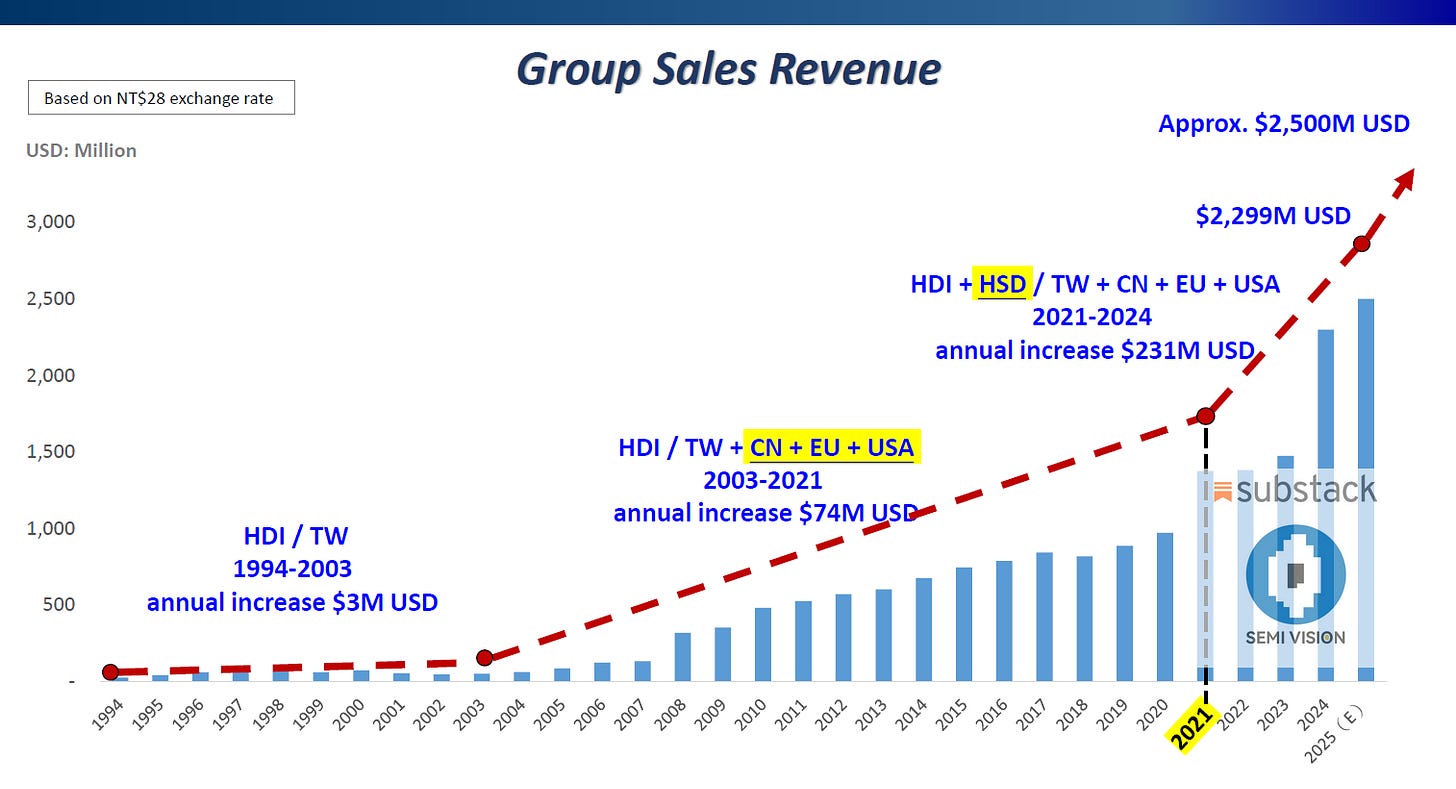
First Inflection Point (2003):
The launch of smartphones in the early 2000s triggered a surge in demand for HDI and halogen-free materials. This pivotal moment expanded our market footprint beyond Taiwan to China, Europe, and the United States. From 2003 to 2021, our group sales revenue grew steadily, with an average annual increase of $74 million USD.
Second Inflection Point (2021):
The global AI server boom marked a new chapter in EMC’s growth. The demand for high-speed, halogen-free materials with low dissipation factor (Df) became essential in AI server infrastructure. This trend significantly accelerated our business, pushing our high-speed material market share from virtually zero to a major contributor. From 2021 to 2024, our annual revenue growth surged to $231 million USD, with projected revenue reaching approximately $2.5 billion USD by 2025.
This exponential growth highlights EMC’s ability to align with technological shifts and capture value from emerging trends in mobile and AI computing.
EMC Group Technology Evolution
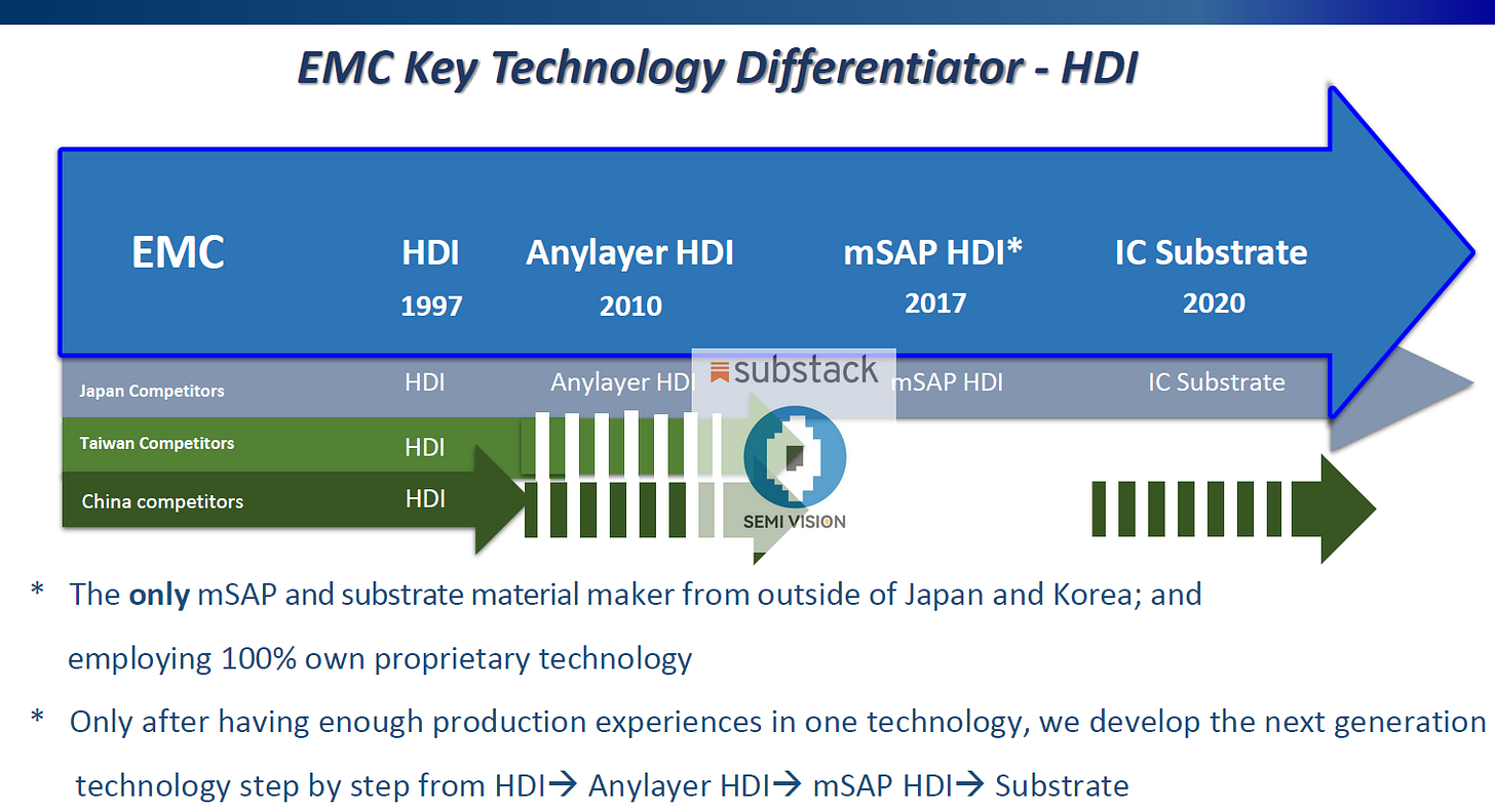
This financial trajectory mirrors our disciplined, step-by-step technology development strategy:
In1997, EMC introduced its first generation of HDI materials.
By2010, we had launched Anylayer HDI, enhancing design flexibility and density.
In2017, we developed our ownmSAP HDImaterials, entering the era of finer line/space performance.
Crucially, EMC has maintained a commitment to only advance to the next generation of materials after gaining sufficient manufacturing expertise and market validation in the prior generation.
By2020, with strong technical and production foundations in place, EMC entered theIC substratematerials space.
What sets EMC apart is our 100% proprietary technology development approach. We do not rely on licensed technologies at any stage. As a result, EMC is the only mSAP and IC substrate material manufacturer outside of Japan and Korea with fully in-house developed capabilities.
This unique positioning—combining deep technical know-how, sequential innovation, and global competitiveness—has enabled EMC to scale rapidly while maintaining leadership in next-generation substrate materials.

EMC Global Ranking in 2023 – Market Leadership in HDI and Halogen-Free Laminates
According to the latest 2024 market intelligence report by Prismark, EMC achieved remarkable global rankings across multiple segments of the laminate material industry in 2023, highlighting our technological leadership and sustained business growth.
Green Laminate Market – Top 3 Globally by Revenue
In the global green laminate market, EMC ranked third worldwide, with annual sales reaching $1.13 billion USD, representing 33% of the total market. This achievement places us just behind ITEQ and TUC. However, it is important to distinguish that both ITEQ and TUC primarily focus on traditional FR-4 laminates, whereas EMC specializes in halogen-free and environmentally friendly materials—a critical differentiation as ESG and low-toxicity standards become increasingly important across the electronics supply chain. Our green laminate solutions are tailored for high-performance computing, 5G infrastructure, and consumer electronics where flame-retardancy and sustainability are key.
HDI Laminate Market – Global No. 1 with 70% Share
In the HDI (High-Density Interconnect) laminate market, EMC holds the dominant global position with a 70% market share, ranking No. 1 worldwide. This leadership reflects our long-term commitment to advanced materials innovation, as well as our strategic focus on miniaturization, high layer-count performance, and reliability standards required by smartphone, tablet, and wearable device makers. EMC’s HDI laminates are also known for their halogen-free formulation, further strengthening our environmental positioning.
As the world’s leading provider of halogen-free and HDI laminate materials, EMC’s success in 2023 marks the culmination of years of deliberate investment in R&D, global customer partnerships, and vertical integration of proprietary technologies. This achievement also validates the effectiveness of our first-phase growth strategy, driven by the rise of mobile devices, and sets a strong foundation as we expand further into high-speed server and IC substrate markets.
EMC – Global No.1 in High-Speed Laminate (2023)
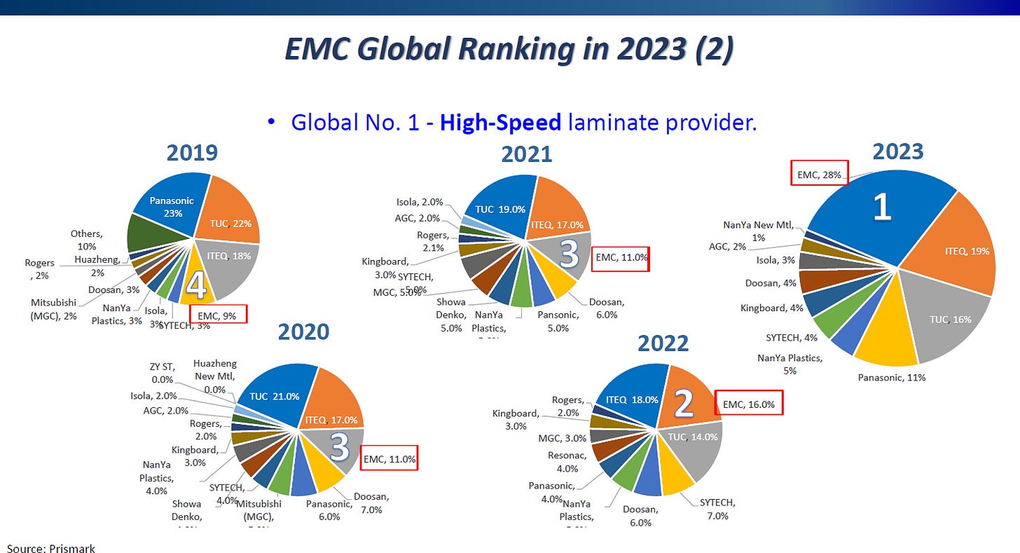
According to Prismark data, EMC has demonstrated rapid and sustained growth in the global high-speed laminate market, moving from a challenger to the clear industry leader within just five years.
In2019, EMC held a9%market share, ranking4thglobally, behind traditional players like Panasonic and TUC.
By2020and2021, EMC had risen to3rd place, steadily expanding its market share to11%, signaling growing adoption of its high-speed, halogen-free materials.
In2022, EMC accelerated its momentum, taking2nd placewith16%share—narrowing the gap with top competitors.
In2023, EMC achieved a significant milestone: rising toGlobal No.1with an impressive28% market share, surpassing ITEQ, TUC, and Panasonic.
This performance is not just a reflection of volume—it signals EMC’s technology leadership and strategic positioning in high-frequency, low-loss laminate materials used in next-generation applications such as:
AI servers, where signal integrity and low dissipation factor (Df) are mission-critical
5G infrastructure, requiring materials with superior thermal and electrical properties
High-speed computing platformsandnetworking equipmentthat demand consistent, scalable laminate performance
EMC’s success can be attributed to several key factors:
100% proprietary technology development, without reliance on external licensing
A clear focus on halogen-free, environmentally friendly formulations
Strong alignment with system-level requirements from Tier-1 customers in the US, EU, and Asia
An agile R&D and manufacturing model that enables faster turnaround on high-mix, high-specification orders
In a market increasingly driven by signal speed, material reliability, and sustainability, EMC has not only caught up with traditional giants—it has redefined the competitive landscape and established itself as the new benchmark in high-speed laminate innovation.

These products are typically categorized as high-end consumer electronics, where performance, miniaturization, and integration are critical. Applications such as 5G smartphones, tablets, wearable devices, HDI notebooks, and DRAM/SSD storage solutions all demand advanced interconnect density, signal integrity, and thermal reliability—requirements ideally met by HDI technology.
EMC has long focused on serving the high-end segment of the market, consistently providing cutting-edge HDI laminate solutions tailored for premium applications. By maintaining technological leadership and deep collaboration with global OEMs, EMC has established itself as the go-to supplier for advanced packaging materials in the most performance-sensitive product categories. This strategic positioning not only secures EMC's dominant market share, but also ensures it remains at the forefront of the industry's evolution toward AI-driven, high-performance electronics.


This slide highlights EMC's rapid ascent to global leadership in High Speed Digital (HSD) and High Reliability (HR) laminate applications—growing from zero to number one in just seven years.
EMC's HSD and HR materials are now the backbone of mission-critical and performance-intensive systems across multiple sectors. These include:
AI Servers: With over 70% market share, EMC’s materials support the high-speed, high-frequency requirements of AI computing infrastructure.
General Servers: Holding over 50% share, EMC enables data center scalability and reliability for enterprise computing.
Network Switches: Also surpassing 50% share, EMC provides robust signal integrity and low-loss materials for high-bandwidth switching hardware.
LEO Satellites: Over 70% market penetration in low-earth orbit satellite systems, where durability and signal stability are vital in harsh space environments.
ADAS (Advanced Driver Assistance Systems): EMC’s laminates power over 50% of advanced automotive electronics, delivering safety-critical performance and long-term reliability.
Defense Industry: With more than 35% market share, EMC supports military-grade systems requiring the highest reliability, thermal performance, and electromagnetic compatibility.
This track record underscores EMC’s strategic commitment to high-end, high-growth sectors where digital transformation and system reliability converge.

EMC’s product roadmap for FCBGA (Flip-Chip Ball Grid Array) and SiP (System-in-Package) technologies, highlighting how substrate material innovation enables computing devices to evolve with increasing I/O density and form factor complexity.
The upward and rightward trajectory reflects the semiconductor industry’s broader trend: as computing power increases and device form factors shrink, packaging becomes more advanced and integration more complex. From early desktop PCs to modern AI and 5G systems, devices require substrates that support higher I/O counts, greater density, and thermal-mechanical reliability.
EMC addresses these challenges through continuous material evolution:
Lower CTE (Coefficient of Thermal Expansion)helps eliminate CTE mismatch between IC and substrate, reducing stress and improving long-term reliability.
Higher Modulusmaterials provide better warpage control, which is critical in large-area, high-density packaging like FCBGA and SiP.
As we move into the AIoT, 5G, and edge computing era, EMC’s materials roadmap positions it to support next-generation integration needs in performance-critical environments.

EMC Product Roadmap for FCBGA/SiP
EMC's advanced material roadmap for FCBGA/SiP packaging, with a strategic focus on deliveringlow XY CTEandhigh modulussolutions—key enablers for next-generation high-density, high-performance semiconductor packages.
Key Observations and Trends:
Shift Toward Lower CTE & Higher Modulus:
As computing power increases and package complexity rises, warpage and thermal mismatch become critical challenges. The industry's direction is clearly moving toward materials with:
CTE < 1 ppm/°C, targeting extreme low thermal expansion
Modulus > 40 GPa, to support warpage control in large-area or multi-die integration
Product Roadmap:
EM-S526: A widely adopted MP (mass production) solution, used extensively in current SiP applications but with higher CTE (~9 ppm/°C).
EM-S570: Combines high modulus and reduced CTE (~5 ppm/°C), well-suited for flip-chip and SiP formats in mass production.
EM-S572T (Q4’25)andEM-S570K3 (Q3’25): New materials under development that push further toward the ideal performance zone—extremely low CTE (<2 ppm/°C)withhigh modulus (>35 GPa). These are tailored for emerging FCBGA/SiP needs in AI, HPC, and edge applications.
EM-S570T: Currently a sample stage product balancing performance for advanced development and qualification.

EMC is clearly positioning itself as a materials innovator in the advanced packaging space. With the upcoming EM-S570K3 and EM-S572T, EMC is targeting the"Extreme XY CTE + High Modulus"zone—essential for enabling the next wave of SiP, HPC, and AI packages that demand dimensional stability, high I/O density, and mechanical robustness.
This aligns with broader industry trends toward glass-core substrates, heterogeneous integration, and AI-centric architectures, where material science plays a pivotal role in system reliability and yield.

EMC’s Product Roadmap for AiP (Antenna-in-Package) and highlights the material innovations and integration trends supporting next-generation wireless communication systems.
What is AiP?
Antenna-in-Package (AiP)refers to the integration of RF front-end components (like power amplifiers, low-noise amplifiers, filters, switches, and transceivers) and theantenna itselfdirectly within the package substrate. This approach eliminates the need for external antenna modules, enabling:
Compact designs
Lower signal loss and shorter transition paths
Enhanced signal integrity and RF performance
Improved system integration and miniaturization
AiP is especially critical in 5G smartphones, mmWave devices, and emerging IoT/automotive radar applications.
Key Industry Trends Reflected in the Image in AiP
RF Front-End Integration:
The left side of the chart shows the traditional RF front-end components surrounding the antenna. EMC’s roadmap is moving toward integrating these elements into a unified system-in-package (SiP), as shown in the FCBGA AiP and FoWLP AiP examples on the right.
Advanced Packaging Platforms:
FCBGA AiP: Suitable for performance-focused devices where large I/O and heat dissipation matter.
FoWLP AiP: Ideal for compact, thin form factors like mobile and wearable devices, with greater flexibility in layout.
Material Innovation – Enabling Future AiP:
The roadmap emphasizessubstrate material evolution, with two main focus areas:
Lower CTE: Critical for handling mechanical stress in unbalanced structures during thermal cycling.
Lower Dk/Df (Dielectric Constant / Dissipation Factor): Essential for minimizing signal loss and improving high-frequency performance in RF signal paths.

EMC’s core products—based on low-loss organic substrates for AiP—align closely with the HDI (High Density Interconnect) category, which offers several critical advantages:
Key Advantages of EMC’s HDI-Based Solutions
Excellent Supply Chain Maturity & Cost Advantage:
Very high maturityensures stable, scalable mass production capacity.
Very low costmakes EMC’s solutions highly attractive for mainstream and high-volume markets like 5G smartphones and Wi-Fi 7 devices.
Superior 5G/6G Readiness:
EMC’s substrate technology is alreadyhighly mature for 5G/6G AiP applications, allowing faster time-to-market and reduced qualification cycles for system integrators.
Material Optimization for AiP:
Throughsubstrate material innovation—lower CTE and low Dk/Df—EMC addresses traditional HDI weaknesses such assignal integrityandhigh-frequency performance, enabling its HDI platform to approach or exceed some fan-out/glass-level specs in RF use cases.
Scalable and Flexible Design Capabilities:
While HDI substrates are not the thinnest (vs. Fan-Out or Glass), EMC compensates withdesign flexibility,shorter transition paths, andbetter signal integrity—especially in FCBGA or RF SiP formats.
While glass and LTCC substrates offer strong RF performance, their cost, complexity, and supply chain immaturity make them less suitable for high-volume applications today. Fan-Out shows promise but is still costlier and harder to scale for passive integration.
EMC’s technology hits a sweet spot—balancing performance, manufacturability, and cost—which is essential for widespread adoption in consumer AIoT, 5G smartphones, and Wi-Fi 6E/7 infrastructure.
EMC leverages the strengths of HDI substrates—high scalability, low cost, and proven reliability—and pushes the boundaries further with advanced material development, positioning itself as a key enabler in the next wave of AiP innovation.
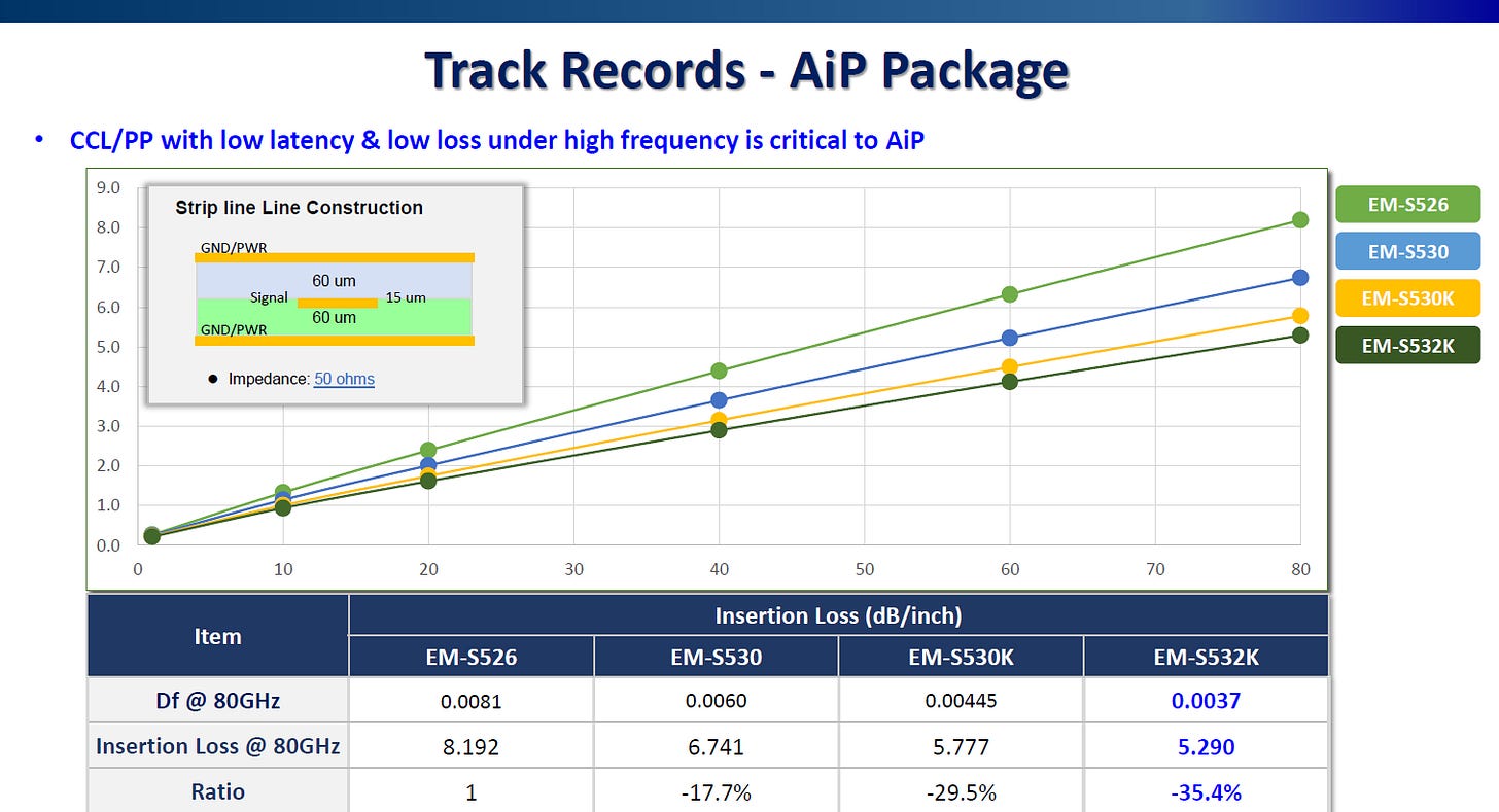
Chart Analysis: Insertion Loss vs. Frequency
The graph showsinsertion loss (dB/inch)across 0–80GHz for four EMC materials:
EM-S526(green) – Baseline reference
EM-S530
EM-S530K
EM-S532K(dark green) – Latest low-loss material
As frequency increases, insertion loss rises across all materials. However, EMC's newer materials significantly reduce signal loss:
EM-S532K achieves 35.4% lower insertion loss at 80GHz compared to EM-S526.
Dielectric loss (Df) drops from 0.0081 (S526) to 0.0037 (S532K), reflecting substantial improvements in material performance.
Trend Insight: Material Evolution for Next-Gen AiP
With mmWave and high-band 5G/Wi-Fi standards pushing system frequencies higher:
Traditional materials like EM-S526, although reliable, face increasing insertion loss and signal degradation.
EMC’s newer generations (S530K and S532K) show a clear material roadmap toward:
Lower Df (dielectric loss)
Improved electrical performance
Enhanced high-frequency signal transmission
As RF system integration shifts into smaller form factors (AiP, SiP, FCBGA) and pushes toward mmWave and sub-THz domains, the demand for ultra-low loss laminate materials is growing fast.
EMC is not just keeping up—it is leading the curve, offering production-ready solutions like S532K that address both today's and tomorrow’s high-frequency packaging challenges.
This positions EMC as a key enabler for next-gen mobile, infrastructure, and AIoT devices.

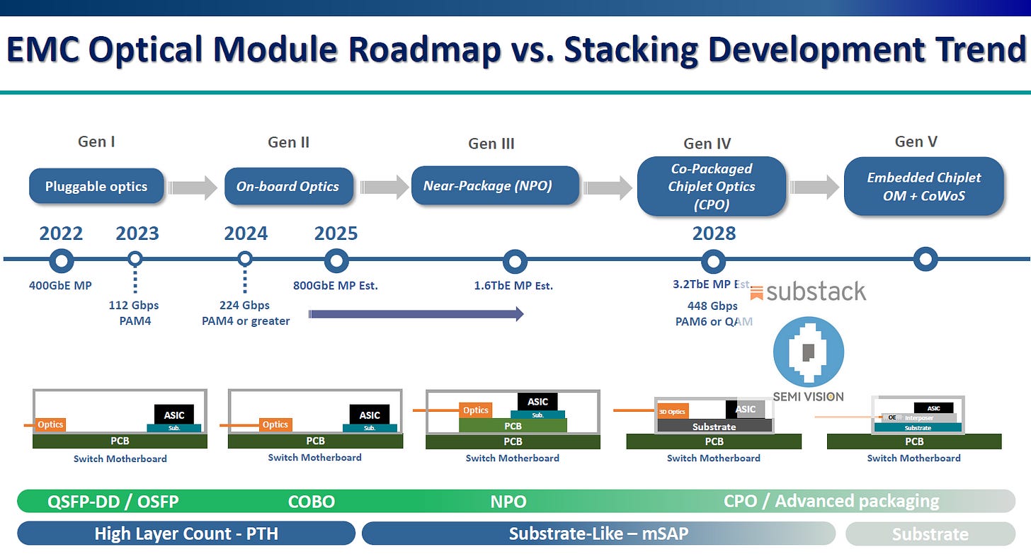
Five Generations of Optical Module Evolution (2022–beyond)
EMC Optical Module Roadmap alongside key stacking and packaging technology trends, illustrating the industry's transition toward higher bandwidth density, lower power, and tighter integration—a direction strongly aligned with the rise of silicon photonics (SiPh).
Gen I: Pluggable Optics (2022–2023)
Modules likeQSFP-DD / OSFPusing400GbE, scaling to112 Gbps PAM4.
Optics and ASICs placedseparately on PCB, with traditional high-layer count substrate (PTH).
Still dominant, but reaching limits in power, latency, and signal integrity.
Gen II: On-board Optics (2024)
Optical engines movecloser to ASIC, reducing interconnect length and improving performance.
224 Gbps PAM4 or higherbecomes the norm.
COBO (Consortium for On-Board Optics) specifications adopted.
Gen III: Near-Package Optics (NPO) (2025)
Optics now integrated near the substrate withsubstrate-like PCB (mSAP).
Prepares for1.6TbEdeployment.
Start of closer photonic-electronic coupling, increasing feasibility for silicon photonics integration.
Gen IV: Co-Packaged Optics (CPO) (2028)
Marks the shift totrue co-packaging: optics and ASICs integrated on thesame substrate.
Enables448 GbpsPAM6 or QAM modulation.
Requires3D optics integration, low-CTE high-performance substrate, and thermal innovation.
Major milestone for silicon photonics—SiPh engines are now directly integrated at package level.
Gen V: Embedded Chiplet Optics + CoWoS (Beyond 2028)
Fully embeddedchiplet optical modules, leveragingTSMC CoWoSor similar advanced packaging.
Enables high-speed, energy-efficient interconnects across chiplets and optical I/O.
SiPh becomes astandard building blockinside data center and AI accelerators.
Silicon Photonics (SiPh): The Key Enabler
As speed scales from 112G → 224G → 448G per lane,electrical interconnects become a bottleneck. Silicon photonics provides:
High-bandwidth, low-loss optical interconnects
CMOS-compatible integrationfor co-packaging with logic
Thermal and power advantagesas density increases
Gen IV and Gen V designs make SiPh-based CPO the centerpiece of next-generation optical modules, enabling hyperscale data centers and AI systems to meet their I/O demands.
Substrate & Packaging Trend
The roadmap moves from traditional PCBs with through-hole vias (PTH) to mSAP and ultimately advanced 2.5D/3D substrates.
EMC’s positioning in substrate innovation (e.g., low CTE, high modulus, optical alignment structures) is crucial for enabling reliable, low-loss optical-electronic integration.
This roadmap shows a clear convergence between optical module evolution, packaging advancement, and silicon photonics adoption. EMC's substrate technologies—spanning high-density interconnects, co-packaging platforms, and future CoWoS-compatible materials—form the foundation of this optical-electronic transformation.
Silicon photonics is no longer an R&D concept—it’s a packaging challenge, and EMC is helping solve it.
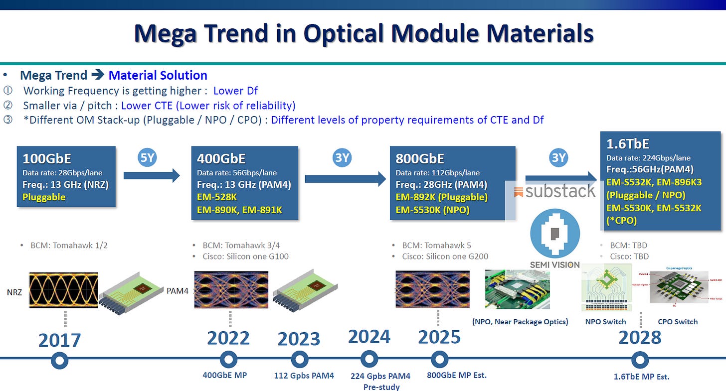
Mega Trend in Optical Module material viewpoints from EMC
The roadmap from 100GbE (2017) to 1.6TbE (2028) clearly reflects a mega trend in both electrical performance and material innovation.
Bandwidth Leap and Frequency Surge
In just over a decade, data rates have grown from 28Gbps/lane to 224Gbps/lane, while operating frequency has surged from 13GHz (NRZ) to 56GHz (PAM4).
This dramatic shift introduces serious challenges in signal loss, latency, and reliability—placing unprecedented demands on optical module materials.
Material Challenges & Solutions
Three key material performance parameters now dominate optical module design:
Df (Dissipation Factor): Lower Df is essential to minimize insertion loss at high frequencies.
CTE (Coefficient of Thermal Expansion): Lower CTE reduces mechanical stress and improves reliability, especially asvia and pitch dimensions shrink.
Compatibility with different stacking architectures: Pluggable, NPO (Near-Package Optics), and CPO (Co-Packaged Optics) each have distinct material needs, especially at high-speed interconnects.
By 2028, the industry is expected to transition toward CPO (Co-Packaged Optics), a key enabler for 1.6TbE and beyond. In this architecture:
Optics and ASIC are co-integrated at the substrate level.
Power, heat, and signal integrity are tightly managed.
EMC’s new materials like EM-S532K are specifically designed to meet the extreme demands of CPO—balancing thermal, mechanical, and RF performance.
The mega trend in optical modules isn’t just about speed—it’s a materials arms race. As line rates double every 3–5 years, next-generation materials like EMC's ultra-low Df and low-CTE laminates are becoming mission-critical. EMC’s portfolio positions it as a leading enabler of the next wave of high-speed optical interconnects, from pluggable to chiplet-level photonics.
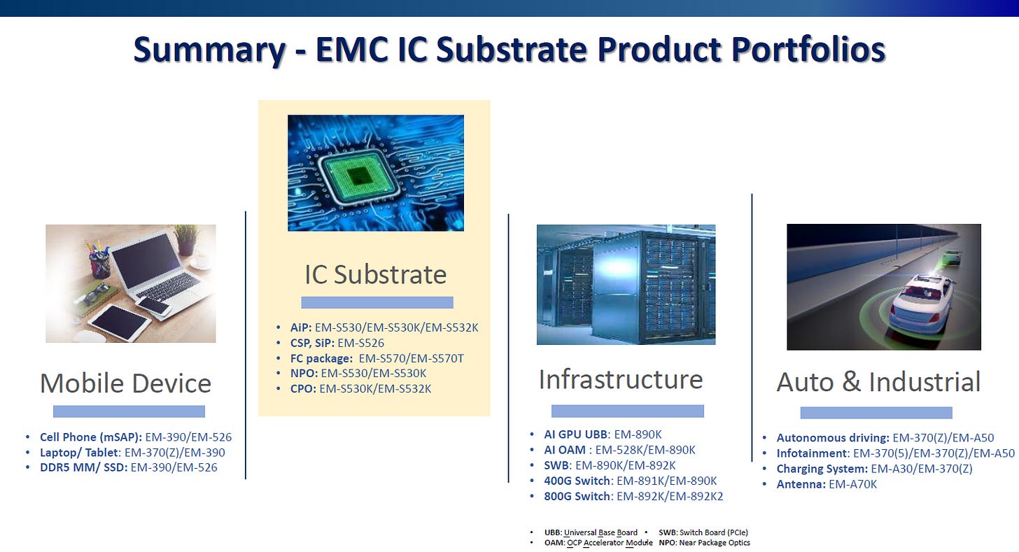
The summary slide provides a comprehensive overview of EMC's IC substrate product portfolio, showcasing its broad application across three major sectors: Mobile Devices, Infrastructure, and Automotive & Industrial. Each segment is supported by a targeted lineup of EMC materials engineered to meet performance, form factor, and integration requirements in next-generation electronics.
Mobile Devices
EMC supports the ultra-thin, high-density needs of smartphones, tablets, and laptops through itsmSAP-compatiblesubstrate materials. Key highlights include:
EM-390 / EM-526for cell phones using modified semi-additive processing.
EM-370(Z) / EM-390optimized for compact laptops and tablets.
EM-390 / EM-526also applied inDDR5 memory modules and SSDs, where signal integrity is critical.
Infrastructure / Data Center
With the rapid expansion of AI workloads and hyperscale data centers, EMC offers a range of high-performance substrate solutions for:
AI GPUsandOAMsusingEM-890KandEM-528K, enabling high power and high speed.
Switch Boards (SWB)such as 400G/800G optical switches, supported byEM-891K, EM-892K.
Near-Package Optics (NPO)andCPOintegration, where low Df and low CTE materials likeEM-S530K / EM-S532Kare essential.
Automotive & Industrial
For future vehicles and industrial automation, EMC offers substrates optimized for:
Autonomous driving ECUsusingEM-370(Z)andEM-A50.
Infotainment systems, where thermal and signal demands are balanced withEM-370(5)andEM-A50.
Charging modulesandantenna units, served byEM-A30andEM-A70K.
Core IC Substrate Applications
EMC’s product lines are tailored to key advanced packaging types:
AiP (Antenna-in-Package): EM-S530, EM-S530K, EM-S532K
CSP / SiP: EM-S526
FC BGA: EM-S570, EM-S570T
NPO / CPO: EM-S530K, EM-S532K
EMC's substrate technologies span across the full electronics spectrum—from ultra-compact mobile devices to AI data infrastructure and automotive intelligence. With a deep focus on low Df, low CTE, high modulus, and integration-ready platforms, EMC is positioned as a core enabler of the next wave of performance-driven and miniaturized systems.


PreviousNext
TopLatestDiscussions








See all