Cooling is the New Architecture: TSMC’s IMC-Si and the Future of AI Packaging
Cooling is the New Architecture: TSMC’s IMC-Si and the Future of AI Packaging
- Source: SemiVision
- Author: SEMIVISION
- Published: 2025-07-03T12:27:14+08:00
- URL: https://tspasemiconductor.substack.com/p/cooling-is-the-new-architecture-tsmcs Cooling is the New Architecture: TSMC’s IMC-Si and the Future of AI Packaging


Cooling is the New Architecture: TSMC’s IMC-Si and the Future of AI Packaging
Original Articles By SemiVision Research (IEEE ECTC , IEEE VLSI , TSMC)

Jul 03, 2025
∙ Paid
Thermal Bottlenecks in the AI and HPC Era: Cooling Becomes the New Compute Enabler

As AI and high-performance computing (HPC) continue to evolve at breakneck speed, the computational capabilities of modern chips are scaling to unprecedented levels. However, the real bottleneck in this race is no longer process node scaling or transistor density—it is thermal management.
With the power consumption of a single AI chip now reaching several hundred to even over a thousand watts, traditional air cooling and indirect liquid cooling solutions are no longer sufficient. Cooling is rapidly shifting from a secondary design concern to a central determinant of system architecture feasibility and energy efficiency.
The future of scalable compute infrastructure will increasingly hinge on our ability to innovate across advanced packaging, materials, microstructural design, and direct cooling techniques.
As such, cooling solutions that move closer to the heat source, along with integrated thermal structures and process-level optimizations, are becoming indispensable to sustaining the growth of AI infrastructure. In this new paradigm, thermal engineering is not an afterthought—it’s a critical enabler of the next compute revolution.
Current Thermal Stack and the Rise of Microfluidic Cooling
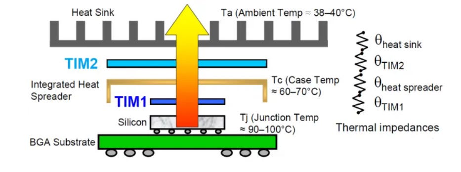
The most common thermal stack in today’s industry consists of:
AI chip + TIM1 + Lid + TIM2 + Cold Plate.
Among these layers, the cold plate is the core of indirect liquid cooling solutions. Its internal architecture, material selection, thermal resistance management, and pressure drop control are all highly complex and critical to overall system performance.
To further enhance cooling efficiency, microfluidic channels have emerged as a promising next-generation solution. By routing coolant directly to areas adjacent to the chip, this method enables rapid heat exchange closer to the heat source, offering lower thermal resistance and potentially much higher cooling efficiency compared to conventional approaches.
TSMC's Direct-to-Silicon Liquid Cooling: Background and Technical Evolution
As early as the 2021 TSMC Technology Forum, TSMC publicly introduced its concept of direct liquid cooling via backside contact with the silicon chip. The proposed solution involves fabricating mesh- or stripe-shaped microchannels on a silicon wafer or Si lid using MEMS processes, and then fusion bonding the structure to the backside of the chip.

Experimental results demonstrated that this approach could support over 2600W of total power and achieve a power density of up to 4.8 W/mm². This pioneering concept laid the technical foundation for the subsequent development of Integrated Microchannel Cooling on Silicon (IMC-Si).
2024 ECTC: TSMC Unveils First Core Paper on IMC-Si Technology
At the 2024 IEEE ECTC conference, TSMC officially presented its landmark paper,“An Energy-efficient Si-integrated Micro-cooler for High Power and Power-density Computing Applications”, revealing for the first time a production-viable and energy-efficient silicon-integrated micro-cooler (IMC-Si) designed for high-performance computing.

Background and Motivation:
According to the 2023 HIR (International Roadmap for Devices and Systems), the average power density of AI/HPC chips has increased from 1.1 W/mm² in 2018 to 2.2 W/mm² in 2023, and is expected to exceed 20 W/mm² within the next decade.
Traditional cooling methods—such as air cooling, cold plates, and immersion liquid cooling—face significant limitations in efficiency, cost, integration complexity, and long-term reliability.
Technical Architecture and Highlights:
Micropillar arraysare etched directly into the backside of the silicon substrate and paired withliquid inlet/outlet (LIO)channels, enablingdirect liquid cooling with no intermediate thermal interface materials (No TIM).
Theelliptical cross-section micropillarsare designed to minimize pressure drop and induce turbulence for improved heat transfer efficiency.
A3×3 compartmentalized microfluidic layoutenables short-path, zoned flow, optimizing cooling performance while reducing pressure loss.
The process isbuilt on TSMC’s SoIC® Wafer-on-Wafer bonding platform, ensuring high compatibility with advanced packaging production lines.
This development marks a key milestone in addressing the thermal bottleneck of next-gen AI and HPC systems, bringing cooling technology much closer to the source of heat—at the silicon level.
2025 ECTC: Integrating Direct-to-Silicon Liquid Cooling onto CoWoS® Platform—A Step Toward Mass Production

Building upon its 2024 technical foundation, TSMC unveiled a major advancement at the 2025 IEEE ECTC with its paper titled“Direct-to-Silicon Liquid Cooling Integrated on CoWoS® Platform”. For the first time, the IMC-Si architecture was successfully integrated into the production-grade CoWoS®-R advanced packaging platform. Key highlights include:
Platform Integration:
Implemented on a 3.3X reticle-size package, simulating a highly integrated layout of 4 SoCs + 8 HBM dies.
Requires only minor modifications to existing CoWoS® process flows, demonstrating strong compatibility with established packaging lines.
Thermal Performance:
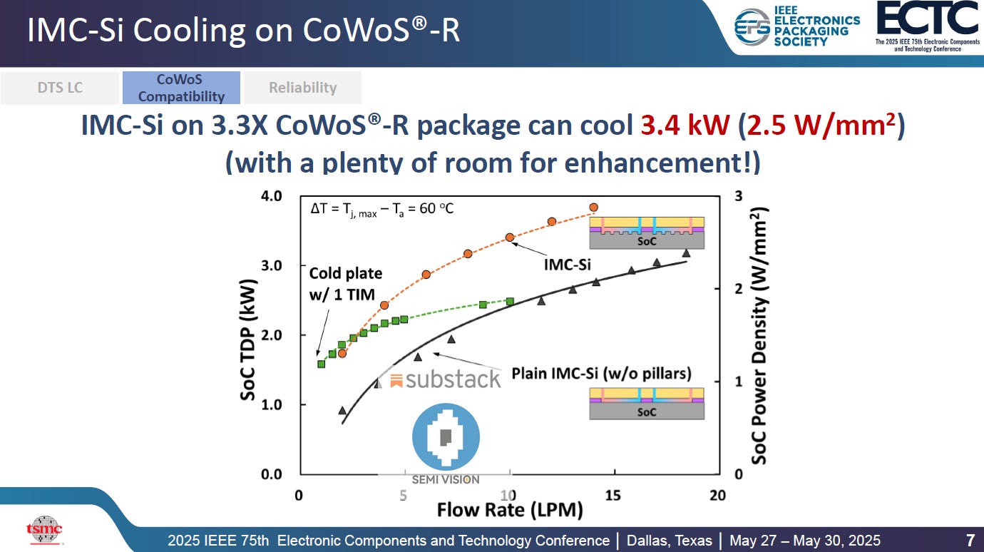
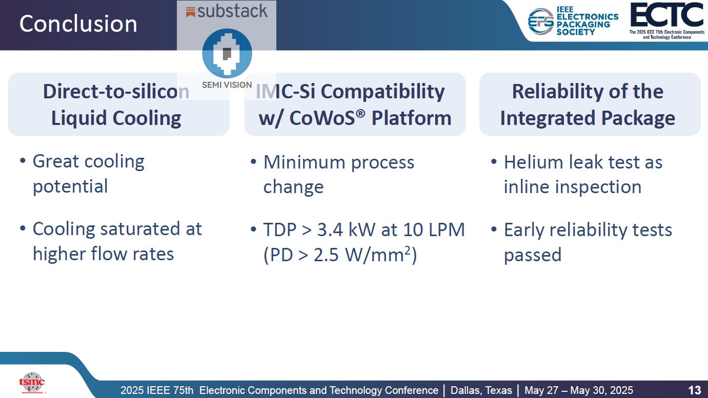
Under 10 LPM water flow at 40°C, the system achieves a thermal design power (TDP) of up to 3.4 kW (2.5 W/mm²).
Both simulation and empirical data show that micropillar structures provide ~50% higher cooling efficiency compared to non-pillar counterparts.
Warpage Tolerance Design:
Utilizes linear-dispensed sealant with high flexibility, enabling tolerance of 160–190 µm of package warpage, effectively mitigating thermal resistance increases or leakage caused by lid deformation.
Seal Reliability Testing:
Evaluated using Helium leak tests per NASA-STD-7012A. The derived water leakage threshold is 115 cc/year.
All tested samples performed well below this threshold, validating long-term seal integrity suitable for data center operation standards.
Evolution of TSMC’s IMC-Si Liquid Cooling Architecture:
2021: Concept proposal and thermal simulation introduced at TSMC Tech Forum.
2024: Thermal performance and energy efficiency of single-die configuration validated, along with process and reliability baselines.
2025: Full integration into production-scaleCoWoS®-Rplatform, demonstrating manufacturability and performance viability in high-power applications.
Looking ahead, further refinement of micropillar geometry and hotspot-targeted cooling paths will be crucial in supporting the next generation of ultra-high-power AI chips. IMC-Si is positioned to become one of the key enabling technologies in the thermal roadmap for advanced computing systems.

In 2024, TSMC presented a paper at ECTC titled"Si-Integrated Micro-Cooler for High Power and Power Density Computing Applications."This work introduced a silicon-based liquid cooling system developed through specialized MEMS processes.

In 2025, TSMC presented a paper at ECTC titled"Direct-to-Silicon Liquid Cooling Integrated on CoWoS® Platform."


For Paid Members: SemiVision Deeply Explores the Strategic Pivot in Thermal Management for Future AI Chips
As high power density and multi-chip integration become mainstream, thermal management is no longer merely an engineering challenge but a core strategic factor shaping the evolution of AI chip architectures. SemiVision will provide an in-depth analysis and value assessment of TSMC’s IMC-Si liquid cooling solution, packaging compatibility design, and the full implementation of the NO TIMs (No Thermal Interface Materials) concept unveiled at ECTC 2025.The content will focus on the following key perspectives:
Trends in AI Chip Architecture and the Shift in Thermal Design Coupling:SoCs exceeding 1000W are becoming reality, fundamentally rewriting packaging strategies previously reliant on air cooling.
The Industry Race Behind the Learning Curve Study:TSMC and its CoWoS® ecosystem are conducting extensive experiments on process and assembly yield learning curves, exploring breakthroughs in thermal bottlenecks through micro-pillar structures, 1D sealant, and interposer-less designs.
The Engineering and Commercial Logic of NO TIMs and Direct-to-Silicon Liquid Cooling:Traditionally indispensable TIM materials are being systematically phased out under high-flow convection and IMC-Si architectures. This is not just an improvement in thermal resistance but a complete redefinition of packaging philosophy.
Frontline Insights from ECTC 2025:Several key papers have clearly indicated that future packaging thermal management strategies will shift from “surface contact conduction” to “chip-level convection.” From thermal interfaces and module designs to process compatibility, everything is being reshaped.
This is not just a technological revolution but a challenge to redefine “packaging as a thermal interface.”

2025年6月27日

2025年5月30日

2025年6月2日
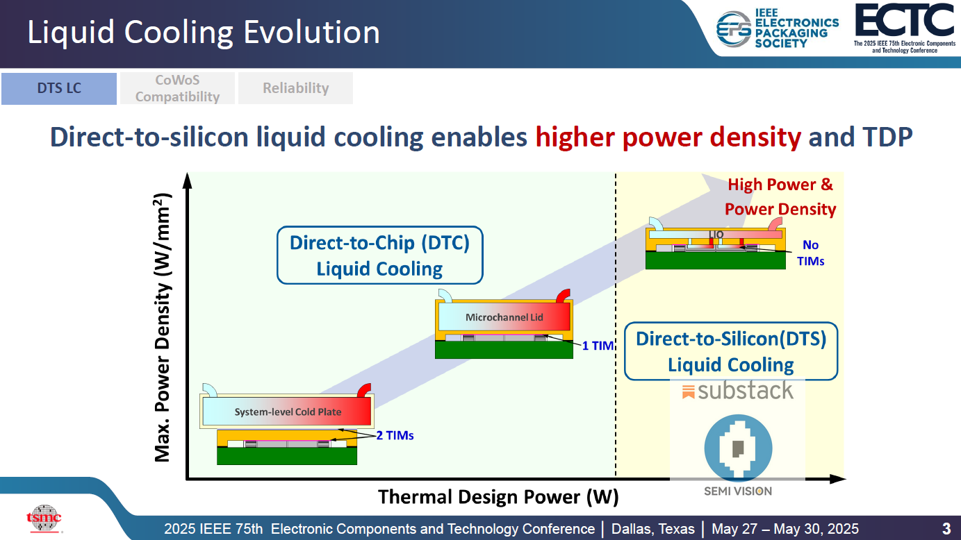
From Cold Plate to Chip: The Next Revolution in Thermal Design
As artificial intelligence (AI) and high-performance computing (HPC) advance rapidly, chip power density has surpassed previous design limits, posing unprecedented challenges to thermal management technologies. In this dual battle of computational performance and energy efficiency, "thermal management" has evolved from a supporting role in system design to a critical factor determining the feasibility of entire platforms.
Traditional thermal solutions often rely on a "system-level cold plate" architecture: coolant flows through a large cold plate to transfer heat to the chip surface, then conducts heat away through two layers of thermal interface materials (TIM1 and TIM2). However, each heat transfer pathway and each layer of interface material introduces additional thermal resistance, contributing to reduced thermal efficiency.
To mitigate these losses, the industry is shifting toward "Direct-to-Chip (DTC)" liquid cooling designs, such as installing a microchannel lid above the chip with a single TIM layer as the thermal medium. This approach significantly enhances heat transfer efficiency and cooling power density.However, the true next step is eliminating TIM materials entirely, achieving a "Direct-to-Silicon (DTS)" liquid cooling architecture where the coolant directly contacts the backside of the silicon chip.In this architecture, the cooling structure is integrated with the chip's backside, utilizing etched microstructures (such as micropillars or microchannel arrays) to enable direct convective heat exchange with the liquid on the silicon substrate. This achieves the lowest thermal resistance and the highest cooling efficiency.
According to TSMC’s latest findings presented at IEEE ECTC 2025, DTS liquid cooling systems can support a total thermal power exceeding 3kW per SoC and a power density of up to 2.5W per square millimeter. More importantly, this design has been integrated with large-scale packaging platforms (e.g., CoWoS®) and has passed validations for package warpage tolerance, hermetic sealing, and high-temperature reliability, demonstrating clear mass-production feasibility.
From system-level cold plates (two TIM layers) to chip-level cooling lids (one TIM layer) and now to DTS architectures (no TIM), this simplification of the thermal pathway not only signifies a significant leap in cooling capacity but also heralds the dawn of a new "thermal-centric" era in advanced packaging design.As AI model scales continue to expand and chip power consumption soars, only by innovating thermal architectures and cooling technologies alongside transistor advancements can the industry unlock the computational potential for the next decade.

Breaking Free from Thermal Bottlenecks: Unlocking the Full Potential of Liquid Cooling Systems
As chip power density continues to rise, the efficiency of cooling systems is rapidly becoming the dominant design factor in high-performance computing platforms. The transition from air cooling to liquid cooling is an industry consensus, but to truly unleash the potential of liquid cooling systems, a critical bottleneck must be overcome: the conduction limit.
In traditional cold plate designs, the heat transfer process from the chip (Tj) to the liquid cooling medium involves multiple layers of thermal resistance: the conduction resistance from the chip to the lid (R_cond), the thermal resistance of the thermal interface material (TIM), and the convection resistance from the liquid to the cold plate (R_conv). Among these, R_cond, constrained by material and packaging structure limitations, is particularly difficult to reduce further, making it the core factor limiting liquid cooling performance.
Even with increased coolant flow rate or improved convective heat transfer coefficient (h), only the convective resistance (R_conv) can be reduced—the bottleneck of conductive resistance (R_cond) remains unchanged. This explains why, even at high flow rates, traditional cold plate systems still experience thermal saturation. As shown in experimental data, when using one or two layers of thermal interface materials (TIM) in a cold plate setup, the power density curve plateaus around 3–4 LPM, limiting further thermal design power (TDP) improvements.
In contrast, the Direct-to-Silicon (DTS) liquid cooling system completely eliminates the intermediate TIM and cold plate layers, allowing coolant to directly contact the backside of the silicon chip, structurally removing R_cond. This architecture shortens the thermal path and unlocks the full potential of convective cooling, enabling linear performance scaling with flow rate without saturation constraints.
Experimental results confirm that under a constant ΔT (Tj - Ta) = 60°C, the DTS system achieves significantly higher power densities than conventional cold plate designs, with substantial headroom even at high flow rates (8–10 LPM).
This breakthrough is more than just enhanced cooling—it redefines thermal scalability for advanced packaging and high-power AI chips. As single-chip thermal design power approaches the kilowatt level, DTS liquid cooling emerges as the only truly scalable, efficient, and integration-ready solution.
From conduction-limited to convection-driven, from passive cooling to co-architected thermal design—this marks a pivotal turning point in next-generation thermal management.
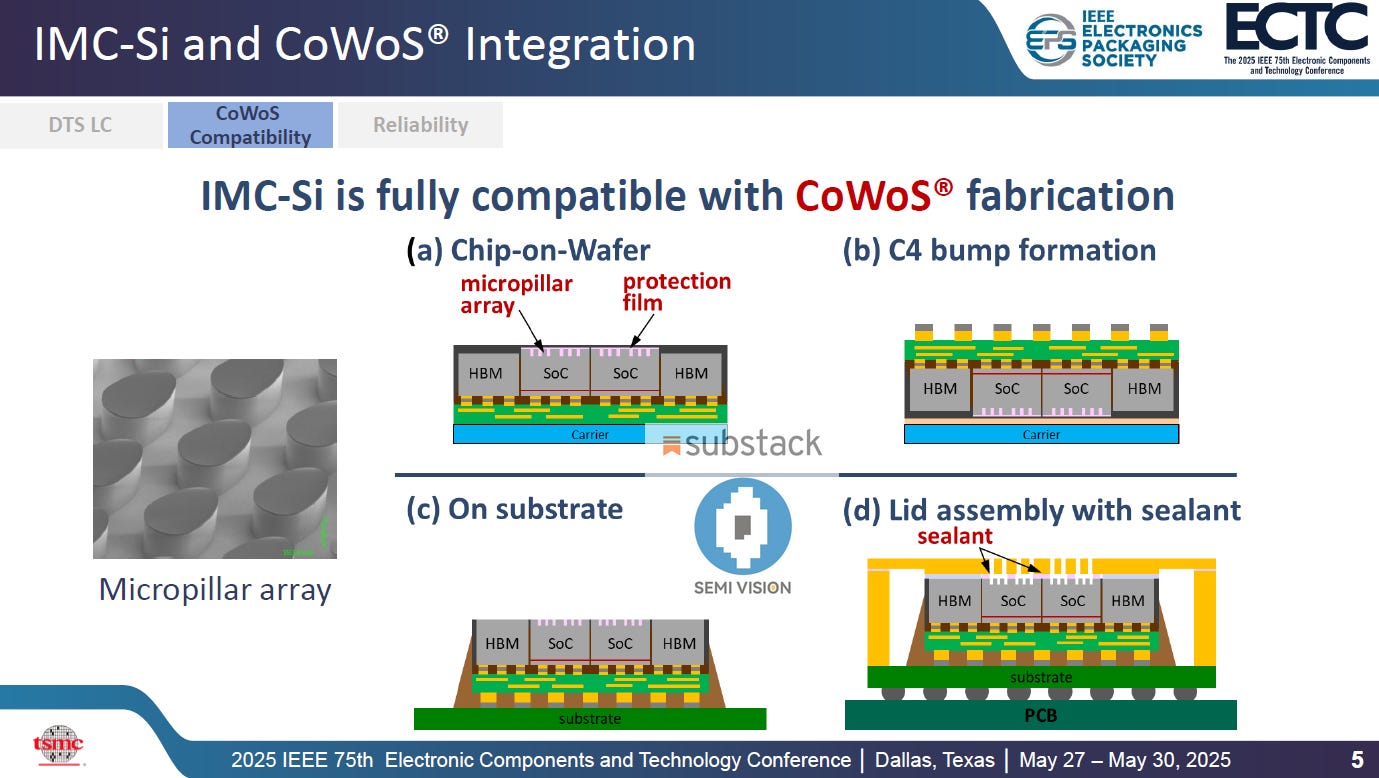
Seamless Integration of IMC-Si with CoWoS® Process: Enabling Mass Production of Chip-Level Direct Liquid Cooling
As AI and high-performance computing (HPC) continue to demand ever-higher power densities from chips, thermal management has become a core challenge in advanced packaging design. Traditional cooling methods are increasingly unable to meet the thermal design power (TDP) requirements in the kilowatt range, prompting the industry to seek solutions that bring cooling closer to the chip’s heat source. TSMC’s proposed IMC-Si (Si-integrated Micro-Cooler) technology is an innovative structure designed precisely to address this critical challenge.
At the heart of IMC-Si is a micropillar array etched directly onto the backside of the SoC die, enabling efficient heat transfer via liquid cooling without the need for thermal interface materials (TIMs). Most importantly, this structure is highly compatible with TSMC’s existing CoWoS® manufacturing process, allowing for seamless adoption of chip-level liquid cooling without significant modifications to the production line.
The complete manufacturing process is divided into four main stages:
1.Chip-on-Wafer Stage
Micropillar arrays are pre-formed on the backside of the SoC die. A temporary protective film is applied to safeguard the micropillars, ensuring they can withstand subsequent high-temperature processing steps.
2.C4 Bump Formation Stage
Conventional C4 solder bumps are formed on the die surface to establish electrical connections between the SoC and the package substrate. This stage does not affect the micropillar structures, ensuring process compatibility.
3.On-Substrate Assembly Stage
The SoC die (with micropillar backside) is integrated with HBM and other memory modules onto the package substrate using standard bonding processes. At this point, the micropillar array remains fully intact on the die backside.
4.Lid Assembly and Packaging Stage
A lid with built-in liquid cooling channels is mounted on top of the chip. A flexible polymer sealant is applied around each SoC die to form a closed liquid-cooling chamber. This design can tolerate deformation caused by package warpage, ensuring both reliability and sealing integrity.
This process not only demonstrates full manufacturing compatibility between IMC-Si and TSMC’s CoWoS® platform, but also highlights its feasibility for mass production and scalability. The technology enables customers to achieve chip-level direct liquid cooling without altering existing packaging architectures, significantly enhancing the thermal power density supported per unit area.
In future high heat-density chip designs, the IMC-Si structure is poised to become a standard solution for integrated cooling and packaging, helping to break thermal bottlenecks and accelerate the deployment of heterogeneous integration and advanced computing platforms.
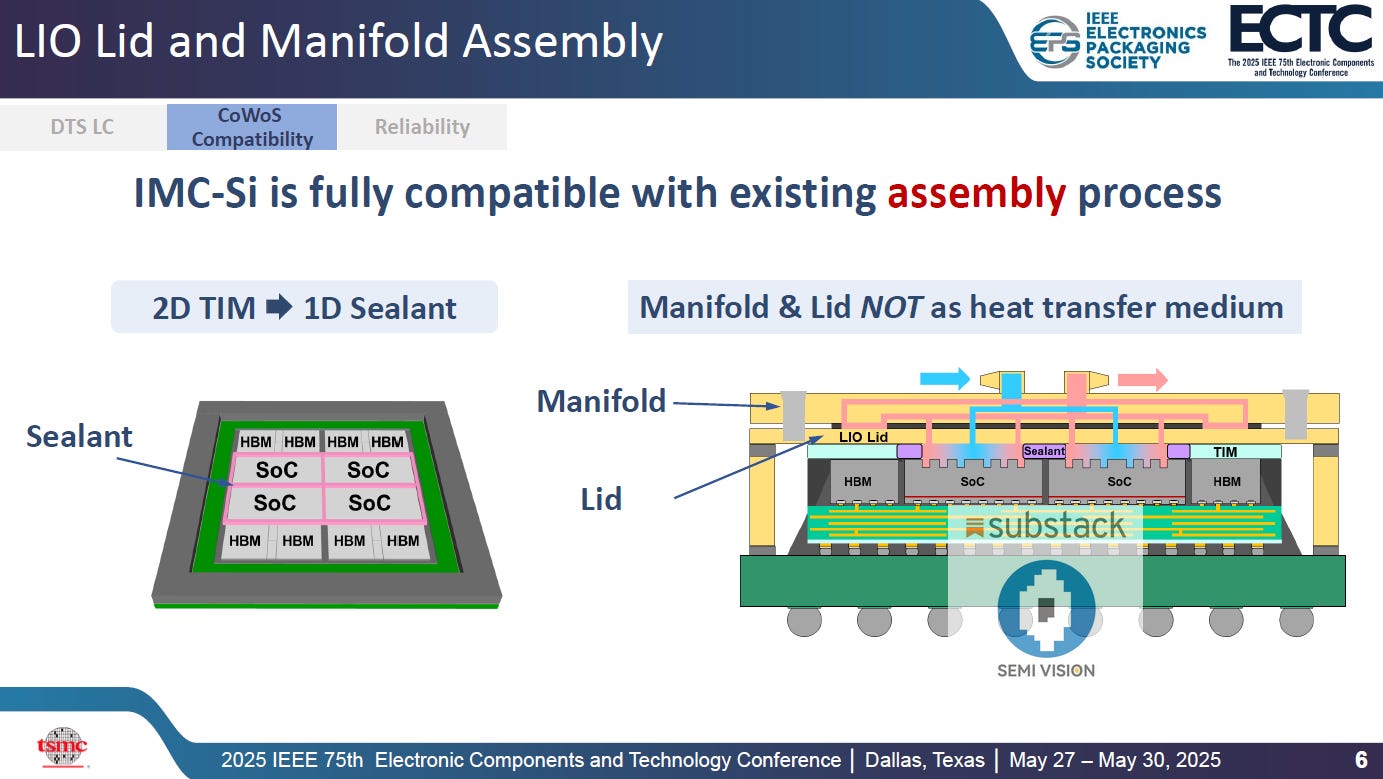
From 2D TIM to 1D Sealant: IMC-Si Redefines Assembly for Liquid-Cooled Packaging
As chip power density rapidly increases, integrating more efficient cooling solutions without disrupting existing packaging workflows has become essential for enabling practical adoption. TSMC’s IMC-Si (Si-integrated Micro-Cooler) liquid cooling architecture not only enhances thermal performance by design but, more importantly, maintains tight compatibility with existing advanced packaging platforms such as the CoWoS® process.
One of the most critical innovations lies in a fundamental shift in assembly methodology. Traditional liquid cooling modules rely on2D area-based Thermal Interface Materials (TIMs)that cover the entire SoC surface between the chip and the cold plate. However, this structure faces challenges with thermal resistance uniformity and long-term reliability, especially under die warpage and large-area packaging.
IMC-Si introduces a radically different assembly paradigm. It employs a 1D linear-application elastic sealant, applied only around the perimeter of each SoC die to form a sealed liquid channel. This structural innovation delivers two major breakthroughs:
Transition from 2D TIM to 1D Sealant: The medium for thermal exchange shifts from the lid to the liquid coolant itself. There is no need to conduct heat through the lid, effectively eliminating the thermal resistance bottleneck imposed by TIMs.
Improved packaging tolerance and reliability: Since the sealant is applied only at the die edges, it effectively absorbs mechanical stress from package warpage, reducing leakage risks and enhancing long-term sealing integrity.
Furthermore, in the IMC-Si architecture, the LIO lid and top-side manifold no longer serve as heat conductors. Instead, they function purely as fluid distribution structures. The coolant flows directly over the micropillar region etched into the backside of the SoC, enabling direct, interface-free heat exchange.
This design allows the integration of liquid cooling into CoWoS® with minimal adjustments to the existing process, preserving high manufacturing compatibility while establishing a new standard for chip-level active cooling.
In essence, this decoupling of the cooling module from the thermal conductivity of the lid signals a shift in thermal architecture philosophy: cooling is no longer dependent on the lid’s ability to conduct heat, but is instead achieved through closer, more precise integration with the chip itself—enabling active, tunable, and efficient thermal management.
Thermal Performance and Scalability of the IMC-Si Liquid Cooling Architecture: A High-Efficiency Solution from Single Die to 3.3X Package Scaling
As chip sizes, stacking layers, and power consumption continue to grow rapidly, traditional cooling systems struggle to meet the increasingly demanding thermal design power (TDP) and power density requirements of high-performance computing (HPC) and AI chips. In response to this challenge, TSMC’s IMC-Si (Integrated Micro-Cooler on Silicon) liquid cooling solution demonstrates significant potential in overcoming the limitations of conventional cold plates and thermal interface materials (TIMs).
Breakthrough Cooling Capability on a 3.3X Expanded Package Platform
According to empirical test results, the IMC-Si architecture achieved a maximum TDP of 3.4 kW on a 3.3X scaled-up CoWoS®-R package platform, corresponding to a power density of 2.5 W/mm², with further room for optimization. Compared to traditional cold plate designs with a single TIM layer, IMC-Si significantly enhances thermal performance by:
Eliminating the thermal conductivity bottleneck of TIMs
Introducing a micropillar array to boost convective heat transfer efficiency
Enabling direct liquid cooling contact with the backside of the silicon die
Contribution of the Micropillar Structure: Significant Performance Gains
Validating Scalability of the Cooling Design
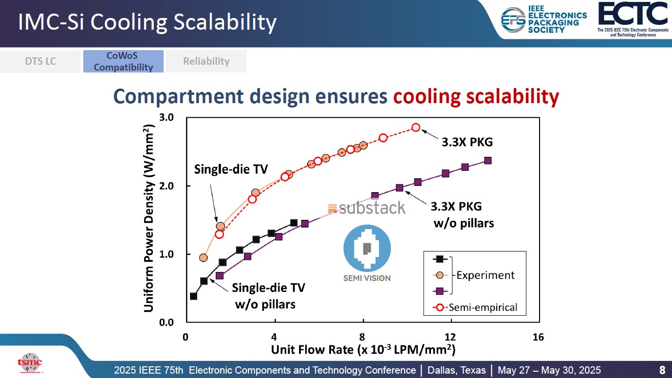
To validate the scalability of the architecture on larger package platforms, TSMC conducted comparisons between a single-die setup and a 3.3X expanded package. Under identical flow rate per unit area (LPM/mm²), the IMC-Si architecture maintained linearly scalable cooling performance, delivering consistent and efficient heat dissipation while avoiding risks such as increased thermal resistance or non-uniform cooling due to scale.
In fact, both empirical data and semi-empirical modeling consistently show that compartment-based flow design and zoned cooling strategies enable IMC-Si to be seamlessly integrated into existing packaging workflows. Moreover, it provides a highly capable and scalable thermal management solution tailored for the escalating thermal demands of future AI and HPC systems.



PreviousNext
TopLatestDiscussions








See all