2025 VLSI-Beyond Scaling: BSPDN Process Innovation through CMP and ALD in the Angstrom Era
本頁目錄
2025 VLSI-Beyond Scaling: BSPDN Process Innovation through CMP and ALD in the Angstrom Era
- Source: SemiVision
- Author: SEMIVISION
- Published: 2025-07-03T11:49:43+08:00
- URL: https://tspasemiconductor.substack.com/p/2025-vlsi-beyond-scaling-bspdn-process 2025 VLSI-Beyond Scaling: BSPDN Process Innovation through CMP and ALD in the Angstrom Era


2025 VLSI-Beyond Scaling: BSPDN Process Innovation through CMP and ALD in the Angstrom Era
Original Articles By SemiVision Research (Samsung , TSMC, Intel ,Nvidia , AMAT , ASM , LAM , TEL , SPTS ,EVG ,EBARA)

Jul 03, 2025
∙ Paid

From Process-Driven to System-Driven: The Path Forward for CMOS Technology in the Ångström Era
As CMOS technology enters the Ångström era, the traditional advantages of dimensional scaling are rapidly diminishing. In his keynote at VLSI 2025, Samsung’s Vice President Keunhwi Cho presented a clear trajectory: the future of CMOS will not be defined solely by smaller nodes, but by multi-level, system-driven innovations across materials, architecture, packaging, and integration.
- Backside Power Delivery (BSPDN): Overcoming Power Integrity Bottlenecks
With increasing power densities and the rise of 3D stacked architectures, conventional front-side power delivery networks (FSPDN) face serious limitations in IR drop and signal interference. Backside Power Delivery offers a transformative solution. By routing power through backside vias (TSVs, BCs, or VBPR structures), BSPDN minimizes resistance and inductance, improves power efficiency, and decouples power and signal paths. Companies like TSMC and Samsung are co-optimizing BSPDN alongside GAA to enhance voltage stability in ultra-dense AI SoCs.
- Heterogeneous Integration: Toward Modular, Functionally Specialized Systems
Heterogeneous integration is becoming the cornerstone of post-Moore innovation. Instead of a monolithic SoC, system architects are embracing chiplets, logic-memory fusion, and sensor integration—each fabricated on the most suitable node. Samsung’s roadmap includes GAA-based logic co-packaged with MRAM, image sensors, and HBM through 2.5D and 3D packaging, enabling modular SoC platforms with high bandwidth, low latency, and domain-specific performance tuning.
- 3D IC: Redefining Density and Performance Amid Thermal and Signal Challenges
3D IC stacking unlocks unprecedented compute density and interconnect proximity. However, it also introduces complex thermal management and signal integrity challenges. Cho emphasizes that advances in lithography alone are no longer sufficient. Next-generation EDA tools must support multi-physics co-simulation—integrating thermal modeling, power network analysis, and die-to-die signal timing—to ensure reliable and scalable 3D systems.
- Silicon Photonics: Enabling Next-Gen Interconnects in the Data-Driven Era
As AI models scale into trillions of parameters, the need for high-bandwidth, low-power interconnects becomes urgent. Traditional copper-based links struggle to meet performance demands across chiplets and memory domains. Silicon Photonics (SiPh) emerges as a foundational technology, offering high-speed optical links with energy efficiency and spatial scalability. Samsung, along with other industry leaders, is investing in SiPh platforms and co-packaged optics (CPO) to embed photonics into logic-memory architectures and data center systems.
Beyond Scaling—The Era of System-Level Co-Optimization
The Ångström era demands more than transistor miniaturization. From backside power delivery and heterogeneous chiplet design to 3D stacking and photonic interconnects, the future of CMOS will be defined by system-level co-optimization. As Cho noted, the real breakthroughs will come not from narrower gate lengths alone, but fromcross-domain collaboration—spanning devices, interconnects, packaging, and architecture. This is how CMOS will continue to evolve beyond Moore’s Law.
For Paid Members ,SemiVision will discuss topics on
Backside Power Delivery: A Key Technology to Solve Metal Congestion and Power Efficiency Challenges
Process Flow of Backside Power Rail (BSPDN)
CMP and ALD: Synergistic Roles in BSPDN
Performance Gains and Technical Challenges in BSPDN
Backside Power Delivery Network (BSPDN): A Strategic Enabler in the Ångström Era of Advanced Semiconductor Manufacturing
1.Samsung: Co-Development of GAA and BSPDN
2.TSMC: Super Power Rail (SPR) as the Industry Benchmark
3.Intel: Commercializing PowerVia Ahead of the Industry
4.NVIDIA: AI SoC Power Demands Drive BSPDN Adoption
5.Applied Materials (AMAT): Backside Process Equipment Leader
6.ASM International: ALD Pioneer for BSPDN Needs
7.LAM Research: TSV and Backside Etch Specialist
8.Tokyo Electron (TEL): Etch and Surface Engineering Innovator
9.SPTS (a KLA Company): TSV & Backside Etch Specialist
10.EV Group (EVG): Enabling Wafer Bonding & Ultra-Thin Processing
11.EBARA’s Role and Value in BSPDN Backside Processing
The Era of Heterogeneous Integration: Chiplet Architectures and the Trillion-Transistor Leap
From N5 to A10: Process Shrink and Packaging Innovation in Tandem
Advanced Packaging and 3D IC: TSV and Hybrid Bonding Usher in a New Era of Heterogeneous Integration
Hybrid Bonding: A Breakthrough for Interconnect Density
3D IC: From Packaging Stacking to a Core Enabler of Performance and Power Efficiency
Silicon Photonics: Redefining Interconnect Architecture for Data Centers
Co-Packaged Optics (CPO): The Future of Silicon Photonics and Switch Chip Integration
Key Elements in TSMC’s Heterogeneous Integration Platform
System-Level Management: Evolving from Functional Verification to Multidimensional Integration and Collaboration
System-Level Thermal Management: Overcoming Thermal Bottlenecks in 3D IC and BSPDN Designs
From Power Delivery to Thermo-Mechanical Co-Design — A New Era for 3D IC Thermal Management

As semiconductor nodes enter the Ångström era, traditional front-side power delivery networks (PDNs) are increasingly becoming performance and power bottlenecks in high-density designs. The backside power delivery network (BSPDN) addresses this challenge by relocating power rails to the backside of the silicon substrate, offering a more efficient, lower-impedance power path while freeing up the front-side interconnect layers for data routing. This significantly improves IR drop, reduces crosstalk, and enhances chip density.
Intel’sPowerViais the industry’s first practical implementation of the BSPDN concept. It is expected to be mass-produced alongsideRibbonFET(a Gate-All-Around architecture) at the 18A and 14A nodes. Testing shows that PowerVia enables over6% frequency improvement, around30% power reduction, and over90% cell utilizationin logic designs. Additionally, the separation of power and signal layers simplifies package design and optimizes routing resources.
In contrast, TSMC’sSuper Power Rail (SPR), introduced at itsA16 (1.6nm-class)node, represents a more advanced implementation of BSPDN. The SPR technology directly connects power rails to the source/drain terminals of each device, incorporating dedicated backside contacts to minimize resistance and maximize power efficiency. According to TSMC, the A16 node offers8–10% frequency improvementor15–20% power savingsat the same performance level compared to N2P, while also improving chip density by approximately7–10%.
Technically, PowerVia employsnano-TSVs(through-silicon vias) to route power from the backside, flipping the wafer to construct a dedicated backside power network. While this increases process complexity, it significantly simplifies the front-side routing and mask layers. TSMC’s SPR, on the other hand, is a more refineddirect-connecttype BSPDN, introducing backside contacts and more precise alignment techniques to enhance PPA (Performance, Power, Area) and thermal management.
In summary, both PowerVia and SPR deliver strong gains in performance, power efficiency, and transistor density. However, SPR is technically more complex and costly to implement. These approaches represent a critical shift in the semiconductor roadmap—from mere node shrinkage towardsystem-driven, power-routing co-optimizationin the Ångström era.
Backside Power Delivery: A Key Technology to Solve Metal Congestion and Power Efficiency Challenges
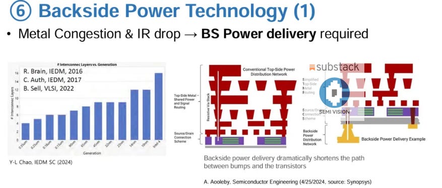
As process nodes advance below 5nm, interconnect structures in chips are facing unprecedented challenges. One of the most critical issues ismetal congestionandIR drop (voltage loss)caused by the rapidly increasing number of metal layers. According to multiple statistics from IEDM and VLSI, the number of metal layers has increased from about 4 layers during the 0.35μm era to more than 14 layers at the 5nm node—and is expected to exceed 16 layers below 3nm.
This evolution has led top metal layers to not only handle high-speed signal transmission but also deliver substantial power, exacerbating routing congestion, complicating power management, and introducing timing uncertainty. In response, Backside Power Delivery (BS-PDN) is emerging as a revolutionary architecture in advanced logic design.
In traditional Top-Side Power Delivery systems, power must enter from the top-side bump and traverse through multiple metal layers and vias to reach the transistor layer. This results in long power delivery paths, significant IR drop, and shared routing layers between power and signals—further limiting signal integration and layout efficiency.
In contrast,Backside Power Deliveryrelocates the power delivery network (PDN) to the backside of the chip, using through-silicon vias (e.g., Power TSVs or similar vertical contacts) to directly supply power near the source/drain region. This architecture offers multiple advantages:
Shorter power paths, significantly reducing IR drop and improving overall power efficiency and transient response.
Freeing up top metal layers, allowing them to be used for signal routing, thus enhancing signal integration density.
Simplifying upper-layer design, reducing metal layer count and process complexity while mitigating RLC effects that cause signal delay and crosstalk.
The structural diagram clearly illustrates the difference: in traditional designs, the red area represents mixed power and signal layers in the top metal stack, which are not only complex but also susceptible to process variation and thermal stress. Under a backside power architecture, power routing (shown in red) is moved to the bottom, dedicated solely to power delivery, creating clearpower/signal decouplingand reducing interference from interlayer routing crossover.
Currently, Intel has implemented a backside power architecture calledPowerViain its 20A/18A nodes as part of its RibbonFET era. TSMC and Samsung also have respective BS-PDN roadmaps, underscoring the growing importance of backside power in advanced logic platforms.
Backside Power Delivery is transitioning from research to real-world implementation and is expected to become a foundational technology for logic platforms below 2nm. By addressing metal congestion, IR drop, and routing limitations, BS-PDN is a critical innovation for continuing Moore’s Law and supporting the growing design complexity of AI and high-performance computing. In the future, when combined with chip stacking, chiplet integration, and heterogeneous packaging, its system-level benefits will become even more significant.
As power density increases and 3D stacking becomes more prevalent, traditional front-side power routing has become a major bottleneck, contributing to IR drop and signal interference. TheBackside Power Delivery Network (BSPDN)addresses these limitations by relocating power rails to the backside of the chip, effectively separating power and signal paths. This improves power delivery efficiency and frees up valuable routing space on the frontside for signal interconnects.
Process Flow of Backside Power Rail (BSPDN)
- Front-End Device and Metal Layer Formation
The process begins with conventional fabrication of transistors and front-side metal interconnects. The M0 layer and dense signal wires are constructed layer by layer on the front side of the chip.
- Carrier Wafer Bonding and Wafer Flipping
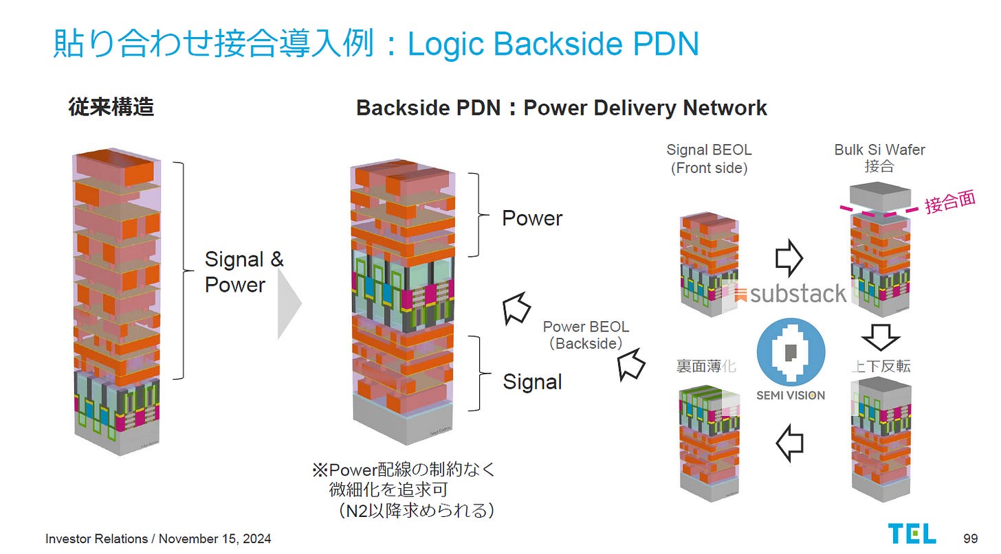
The wafer is then bonded to a carrier substrate and flipped. The backside is thinned through grinding andChemical Mechanical Planarization (CMP)to reduce the remaining silicon to ~500 nm or less.
Note:At this stage, controlling CMP-inducedsurface roughness and warpagebecomes critical, especially for TSMC’s ultra-thin implementations.
- Nano-TSV / µ-via Formation
Next,nano-TSVsormicro-viasare etched from the backside through the silicon to reach either the signal routing layer or thesource/drain contact layer.
Intel’s PowerViaconnects TSVs to the contact layer.
TSMC’s SPRdirectly connects to each source/drain terminal (a “direct-connect” approach), which maximizes efficiency but requiresextremely precise alignment.
Challenges include:Lithography under wafer warpage,critical dimension (CD) control,alignment accuracy, anddeep reactive ion etching (DRIE)process tuning for TSVs. Alignment between thedevice waferandpower rail wafermust be nearly perfect.
- Backside Power Metal and Redistribution Layer (RDL)
After via formation, multiple power metal layers are deposited on the backside, along with theredistribution layers (RDL).
InPowerVia, the backside acts as a centralized power grid accessed through TSVs.
InSPR, each transistor receives a dedicated power contact, enabling thelowest resistance and highest efficiency.
- Pre-Packaging Electrical Validation
Before packaging, a suite of tests is performed to ensure performance and reliability, including:
IR drop simulation
Power integrity analysis
Thermal profiling
Functional validation
These steps ensure that BSPDN not only delivers superior power efficiency but also maintains mechanical and electrical integrity at advanced technology nodes.。
CMP and ALD: Synergistic Roles in BSPDN
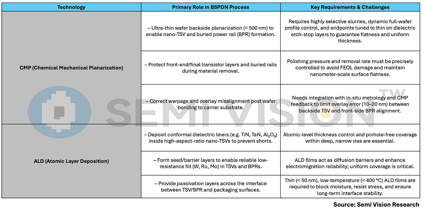
In the BSPDN (Backside Power Delivery Network) process,Chemical Mechanical Planarization (CMP)andAtomic Layer Deposition (ALD)are essential, tightly coupled technologies. CMP plays a critical role in ultra-precise backside thinning and planarization, ensuring proper alignment and manufacturability for downstream processes such as nano-TSV, metal fill, and RDL formation. ALD, on the other hand, enables atomic-scale control of thin film layers—covering everything from barrier and seed layers to dielectric insulators and passivation coatings—ensuring uniformity, conformality, and precision across high-aspect-ratio features.
Together, CMP and ALD form the process foundation that enables BSPDN’s promise of low-impedance, high-efficiency, and reliable power delivery in advanced logic platforms.
- Front-End Fabrication and Buried Power Rails (BPR)
The process starts with conventional front-end CMOS device fabrication, including FinFET or GAA transistor structures and standard front-side metal layers. Simultaneously,Buried Power Rails (BPRs)are embedded within the lower metal layers. These rails are typically filled with materials like tungsten (W) or ruthenium (Ru), embedded within low-k dielectrics. BPRs, with widths around 30 nm and pitches of ~100 nm, provide efficient power delivery paths to source/drain terminals.
- Wafer Bonding, Flipping, and Backside Thinning
After front-end processing, the wafer is bonded to acarrier wafer(often using SiCN fusion bonding). The bonded wafer is then flipped and undergoesback grindingandCMPto thin down the silicon to just a few hundred nanometers—often near aSiGe etch-stop layer. At this stage, minimizingsurface roughnessandwarpageis essential to ensure precise alignment in downstream via etching and metallization.
- Backside Nano-TSV / Micro-Via Formation
With the wafer flipped and thinned,nano-TSVs (nTSVs)ormicro-viasare etched vertically from the backside to reach either the BPR layer or directly to the source/drain terminals:
Intel’s PowerViaarchitecture routes nTSVs to the buried power rail, which then distributes power to logic cells.
TSMC’s SPR (Super Power Rail)employs a more refineddirect-connectmethod, where each transistor’s source/drain terminal is individually connected to the backside power line, achieving optimal resistance and delivery efficiency.
This stage is one of the most challenging, as it demandsnanometer-level alignmentbetween TSVs and device layers. Lithography under warpage conditions, CMP surface control, andDRIE (deep reactive ion etching)uniformity are critical bottlenecks to manage.
- Backside Metal and Redistribution Layer Construction
Once the vias are formed, multiple backside metal layers andRedistribution Layers (RDL)are deposited:
InPowerVia, the backside metal layers form a centralized power grid, delivering current through TSVs to the BPR.
InSPR, each transistor cell features a dedicated backside contact, enabling ultra-low resistance and high-efficiency power routing.
- Pre-Packaging Validation and Reliability Testing
After constructing the backside power network, several validation steps are performed:
IR drop simulations
Power integrity (PI) analysis
High-temperature reliability testing, including JEDEC TQV and thermal cycling, to ensure robustness in real-world operating conditions.
Performance Gains and Technical Challenges in BSPDN
PPA Advantages
At the 18A node, Intel’s PowerVia has demonstrated performance improvements of6–10% frequency gain,25–30% power reduction, and improved logic cell utilization. TSMC’s A16 SPR shows comparable or better frequency/power benefits, with7–10% higher transistor density.
Process Complexity
BSPDN introduces multiple high-complexity steps, including wafer flipping, ultra-thin backside processing, high-precision TSV etching, and direct-connect alignment within single-digit nanometer tolerances—all of which increase cost and yield risks.
Stress and Thermal Management
The addition of backside metal and TSV structures introduces new thermal gradients and mechanical stress challenges. These must be co-optimized with thermal models and physical design rules to maintain nanosheet/GAA device reliability.
BSPDN represents a critical shift from “scaling-only” tosystem-level co-design of power and interconnects. Intel’s PowerVia and TSMC’s SPR reflect two distinct approaches to BSPDN implementation: the former leverages a modular TSV + BPR framework, while the latter pushes efficiency with direct transistor-to-backside connectivity. While both involve high manufacturing complexity, their impact on performance, power, and density positions BSPDN as an essential enabler for Angstrom-era AI SoCs and high-performance computing platforms.
Backside Power Delivery Network (BSPDN): A Strategic Enabler in the Ångström Era of Advanced Semiconductor Manufacturing
As the semiconductor industry enters the Ångström era, theBackside Power Delivery Network (BSPDN)has emerged as a breakthrough technology to overcome the limitations of traditional frontside power and signal routing. The following summarizes the roles and contributions of key players—Samsung, TSMC, Intel, NVIDIA, and leading equipment suppliers such asApplied Materials (AMAT), ASM, LAM Research, TEL, SPTS, EV Group (EVG) and EBARA—in the advancement of BSPDN.
1.Samsung: Co-Development of GAA and BSPDN
Samsung has been a long-time pioneer inGAA (Gate-All-Around)technology, achieving mass production of its MBCFET at the 3nm node. The company is concurrently developing and integrating BSPDN technologies, although it has not officially named its platform (unlike Intel’s PowerVia or TSMC’s SPR). Samsung has disclosed its efforts in embedding power delivery paths and backside conduction schemes aimed at mitigating thermal and routing density bottlenecks. These efforts are expected to be integrated with future 2nm GAA processes. Samsung has also showcased these developments at major conferences such asIEEE VLSI, ECTC, and IITC.
2.TSMC: Super Power Rail (SPR) as the Industry Benchmark
TSMC is arguably the most active and technically advanced company in the BSPDN space. ItsSuper Power Rail (SPR), introduced in the A16 process node, is considered a leadingdirect-connect BSPDNapproach. SPR connects power directly to each transistor’s source/drain vianano-TSVsand backside contacts, enhancing power efficiency, reducing IR drop, and freeing up frontside routing space. TSMC has concurrently strengthened its backside grinding, nano-TSV drilling, metal deposition, and developed thermal-mechanical co-design verification tools. While TSMC’sN2 node uses GAA, theA16 integrates GAA + SPR, andA14 uses GAA without SPR, suggesting a likelydual-track strategybeyond N2.
3.Intel: Commercializing PowerVia Ahead of the Industry
Intel was the first major chipmaker tocommercialize BSPDNwith itsPowerViaarchitecture in the20A/18Aprocess nodes, integrated alongsideRibbonFET. PowerVia leveragesnano-TSVandBuried Power Rail (BPR)to achieve centralized backside power delivery. Real-world tests showed~30% power reductionand6–10% performance gains, while simplifying frontside metal stack complexity. Intel sees PowerVia as a key enabler for extending Moore’s Law and has begun exploring co-integration with advanced packaging technologies likeEMIBandFoveros.
4.NVIDIA: AI SoC Power Demands Drive BSPDN Adoption
Although not a foundry,NVIDIAis a significant driver for BSPDN due to its extreme power demands. AI chips likeB100 and B200now consume up to1000W, placing unprecedented strain on power integrity and thermal design. NVIDIA, in collaboration with TSMC, is exploring SPR adoption for bothCPO switchesandGPU SoCs, while also developingSi-integrated micro-coolersto co-optimize with BSPDN. Given thatCMOS is temperature-sensitive, BSPDN offers a compelling solution for improving transistor density and reliability under high thermal loads.
5.Applied Materials (AMAT): Backside Process Equipment Leader
AMAT plays a vital role in providing tools forCMP, PVD, ALD, and Etch, all essential to BSPDN. It has developed proprietary solutions forultra-thin wafer CMP,deep via etching, anduniform backside metallization, tailored to supporthigh aspect ratio nano-TSVs. AMAT’s integratedbackside modulesstreamline processing by combining CMP, etching, and deposition in a single flow.
6.ASM International: ALD Pioneer for BSPDN Needs
ASM leads inAtomic Layer Deposition (ALD)equipment, which is crucial for BSPDN applications likenano-TSV liners,barriers, andbackside metal isolation. Its conformal ALD technologies can deposit high-k dielectrics and thin metal films (e.g.,Ru, TiN) for thermal and electrical stability. ASM is actively collaborating withIMECandTSMCon BSPDN integration.
7.LAM Research: TSV and Backside Etch Specialist
LAM Research is renowned for its expertise inhigh-aspect-ratio (>10:1) TSV etchingand has optimizedplasma etch systemsto address post-thinning challenges in backside processing. In BSPDN, its hybrid etching flows enhance via uniformity, minimize byproducts, and support multilayerRDL (Redistribution Layer)applications. LAM also offers solutions for via cleaning and protection.
Lam Research ECD: SABRE®
Lam’sSABRE® product familyrepresents its flagshipelectrochemical deposition (ECD)solution, precision-engineered forcopper damascene manufacturing—a foundational technology inadvanced memory, high‑bandwidth memory (HBM), and logic interconnect applications .
Key Capabilities & Advantages:
Deliversvoid-free copper fillacross a wide range of feature geometries, especiallyhigh aspect ratio (HAR)structures, withhigh throughput and robust bottom-up growth.
Offers thewidest process window, exceptionalseed layer protection, uniform deposition across wafers, and optimized edge exclusion to maximize die yield per wafer .
Includes tuned variants likeSABRE® Extreme,Max, andExcel, each tailored for specific throughput, feature size, and fill-rate requirements .
Foradvanced packaging and wafer-level packaging (WLP), Lam also provides theSABRE® 3D family, which extends Electrofill® technology to supportTSVs, copper pillars, RDLs, andmicro-bumps. It features modular architecture and advanced pretreatment chemistries to ensurevoid‑free plating, high uniformity, and cost-effectivenessfor high-density interconnect designs
8.Tokyo Electron (TEL): Etch and Surface Engineering Innovator
TEL provides a comprehensive portfolio of tools forbackside etching (e.g., DRIE),surface planarization, andfine pattern transfer. Its strength lies in coordinatingCMP and photomask alignment, ensuring high patterning accuracy for BSPDN. TEL also supportsultra-thin wafer transport systems, in collaboration with Japanese IDMs, to enable robust backside processing.
9.SPTS (a KLA Company): TSV & Backside Etch Specialist
SPTS focuses onTSV formation,via reveal, andlow-damage etching, making it well-suited for BSPDN processing ofultra-thin wafers. Its dry etch platforms are praised for precise SiGe stop-layer removal andthickness-controlled backside etching. SPTS supportshigh-throughput 300mm BSPDNprocess lines and collaborates on high-volume backend integration.

10.EV Group (EVG): Enabling Wafer Bonding & Ultra-Thin Processing
EVG is the global leader inwafer alignment and bonding, essential for3D IC, TSV, and heterogeneous integration. ItsTemporary Bonding/Debonding (TDB)platforms are key forhandling ultra-thin wafersduring backside processing in BSPDN. This prevents wafer breakage while enabling grinding, via etch, and metallization.
EVG also providesSmartNIL® nanoimprintand theEVG®850 TB/DBseries, which facilitate CMP alignment and warpage control. Itslow-temperature bondingtechnologies are instrumental in integrating BSPDN with GAA, and it plays a pivotal role in projects led byTSMC, IMEC, andFraunhofer.
This overview demonstrates how BSPDN is rapidly becoming the backbone of next-generation logic scaling, demanding tight collaboration betweendevice architects, foundries, and equipment vendors. As AI workloads push power and thermal boundaries, BSPDN will be central to ensuring sustainable performance in the Angstrom era.

11.EBARA’s Role and Value in BSPDN Backside Processing
Backside Wafer Grinding and CMP Technology:
EBARA offers high-precision CMP systems and slurry-free bevel polishing tools for ultra-thin wafer processing, minimizing edge cracks and defects while improving overall yield.
Dry Vacuum Pumps and Environmental Control:
Its dry vacuum pumps and gas abatement systems support clean processing environments, essential for backside wafer operations.
High Market Share and Global Support:
As the world’s second-largest supplier of CMP and vacuum pump systems, EBARA serves over 80% of major semiconductor manufacturers, providing global service infrastructure and high-reliability tool maintenance.


The Era of Heterogeneous Integration: Chiplet Architectures and the Trillion-Transistor Leap
As advanced semiconductor nodes move below 3nm, traditional monolithic chip designs are reaching physical and manufacturing limits. Under the growing challenges of yield, cost, thermal design, and scalability,heterogeneous integrationhas rapidly emerged as a core enabler for next-generation AI and high-performance computing (HPC) platforms.
The evolution of heterogeneous integration can be summarized in three key directions:chiplet modularization, multi-function integration, and diverse customization. These strategies enable system-level designs that are no longer constrained by single-die size or yield. Instead, multiple dies with different functionalities (logic, memory, I/O, AI accelerators) are integrated into a unified platform via advanced packaging techniques likeCoWoS, InFO, and SoIC, providing greater scalability and flexibility.
From N5 to A10: Process Shrink and Packaging Innovation in Tandem
As shown in the timeline, since the 5nm (N5/N4) era began in 2020, the industry has simultaneously pushed forward both process miniaturization and packaging innovation. With continued progression through N3, N2, A14, and A10 nodes, chip integration strategies have evolved from monolithic designs to3D chiplet-based architectures, enabling designs with over100 billion (100B) to 1 trillion (1T) transistors.
3D heterogeneous integration allows engineers to optimize each sub-module with the most suitable process node—for example, using cutting-edge GAA nodes for compute logic, mature nodes for SRAM or HBM, and cost-effective nodes for I/O or PHY—thereby improving overallPPAC (Performance, Power, Area, Cost)efficiency.
Realizing the Trillion-Transistor Era: NVIDIA Blackwell Hits 208B
NVIDIA's new Blackwell GPU platform exemplifies the power of heterogeneous integration. It features a staggering 208 billion transistors and achieves 20,000 TFLOPS of single-precision performance—far surpassing the previous Hopper H100 (80B, 4000 TFLOPS) in both compute density and energy efficiency.

Comparing GPU generations from NVIDIA since 2016:
Pascal (2016): 15.3B transistors, 19 TFLOPS
Volta (2017): 21.1B, 130 TFLOPS
Ampere (2020): 54.2B, 620 TFLOPS
Hopper (2022): 80B, 4000 TFLOPS
Blackwell (2024): 208B, 20,000 TFLOPS
In just eight years, both transistor count and compute performance have grown by orders of magnitude—demonstrating that chip innovation is no longer solely driven by process scaling, but increasingly by architectural and packaging breakthroughs.
Industry Implications and Future Outlook for Heterogeneous Integration
Heterogeneous integration is not just a technical breakthrough; it marks a paradigm shift for the semiconductor industry. As AI models exceed 1 trillion parameters and data/bandwidth demands explode, monolithic SoCs can no longer meet performance and scalability needs.
Chiplet architectures offer flexible composition of IP blocks, memory modules, and compute engines, allowing customization for inference, training, edge, or data center scenarios. This also reduces design reuse complexity, accelerates testing, and shortens time-to-market.
On a technical level, heterogeneous integration is accelerating the adoption of enabling technologies such as TSV, SoIC, 2.5D/3D IC packaging, optical interconnects, and backside power delivery (BSPDN)—paving the way for “More than Moore” era innovation.
Heterogeneous integration is moving from research to mainstream AI chip design practice. Through chiplets, 3D packaging, and cross-node integration, it not only enhances performance and scalability, but also lays the hardware foundation for ultra-large AI models and next-generation data centers.
Looking ahead, we will see more “System-in-Package” (SiP) design philosophies that drive the semiconductor industry into the true era of trillion-transistor integration.
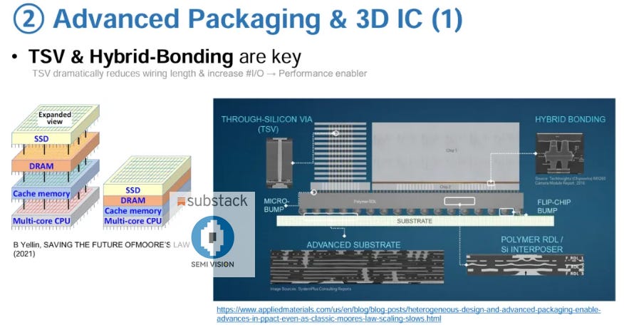
Advanced Packaging and 3D IC: TSV and Hybrid Bonding Usher in a New Era of Heterogeneous Integration
As traditional process scaling approaches physical limits, the semiconductor industry is rapidly shifting its focus to packaging-level innovations to continue Moore’s Law. Among these, 3D Integrated Circuits (3D ICs) and advanced packaging technologies have become critical for integrating logic and memory systems. Two core pillars driving this transformation are Through-Silicon Via (TSV) and Hybrid Bonding.
3D Heterogeneous Integration: Vertical Integration Across Functional Blocks
Heterogeneous integration is not only an extension of process scaling—it is also the foundation for a“System-in-Package (SiP)”paradigm. The diagram illustrates a typical 3D stack system, vertically integrating multiple functional layers such as CPU cores, cache memory, DRAM, and even SSD storage. This vertical stacking enables the creation of high-performance, high-bandwidth computing platforms.
The key advantage of this structure lies inshortening signal transmission paths,boosting data throughput, andreducing power consumption, making it especially valuable in AI, HPC, memory stacking, and edge computing applications.
TSV: Enabling High-Speed Vertical Interconnects
Through-Silicon Via (TSV)technology allows signals and power to penetrate vertically through the silicon die, replacing traditional long lateral interconnects routed through the package substrate. The benefits include:
Shorter interconnect paths: Significantly reduces latency and power consumption.
Higher I/O density: Supports more communication channels, ideal for high-speed memory like DRAM or HBM.
Enhanced 3D packaging scalability: Enables deeper stacking and tighter integration across layers.
TSV is the foundational technology for high-speed DRAM packaging (e.g., HBM) and is widely used in dense logic modules and edge computing platforms.
Hybrid Bonding: A Breakthrough for Interconnect Density
Complementing TSV, Hybrid Bonding combines copper-to-copper (Cu-Cu) and oxide-to-oxide bonding to achieve:
Ultra-high interconnect density: Interconnect pitch as low as 1–3 µm, far exceeding traditional flip-chip bump pitches.
Low contact resistance: Enables high-speed, low-power signal transmission, ideal for high-performance logic and memory.
Precise alignment capability: Supports die-to-die and wafer-to-wafer stacking with high accuracy.
Hybrid bonding has become a foundational technology for modern high-end packaging platforms like TSMC’s SoIC and Intel’s Foveros, transitioning from bump-based assembly to bump-less direct bonding.
Evolution of Packaging Platforms: From RDL to Interposer
To support TSV and hybrid bonding, advanced packaging platforms are evolving in parallel:
Polymer RDL (Redistribution Layers): Provide fine-line routing, widely used in fan-out packaging.
Silicon Interposer: Offers flat surfaces and multi-layer metal routing for high-speed chip integration (e.g., CoWoS).
Advanced Substrate: Enables multi-die stacking and ultra-wide bandwidth interfaces, crucial for chiplet-based systems.
These structures elevate packaging from a passive post-fabrication step to a primary enabler of system-level performance, power, and area optimization.
TSV provides the foundational vertical interconnects for 3D ICs, while Hybrid Bonding pushes the limits of interconnect density and signal integrity. Together, they enable the high-integration demands of AI, HPC, and next-generation SoC designs. As Moore’s Law scaling slows, these advanced packaging technologies are redefining semiconductor innovation—ushering in an era where “packaging is the system” and “packaging is performance.”
3D IC: From Packaging Stacking to a Core Enabler of Performance and Power Efficiency
As chip complexity and die sizes increase, traditional 2D SoC designs are hitting limitations in performance, power, and area (PPA). Today, 3D Integrated Circuit (3D IC) technology—once seen as a supplementary path to extend Moore’s Law—has evolved into a proactive enabler of system-level performance and energy efficiency.
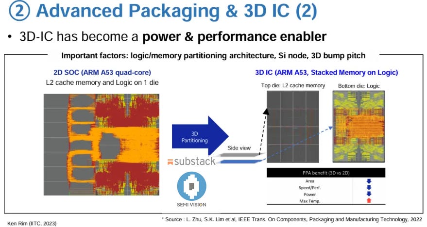
The diagram compares two designs based on the same ARM Cortex-A53 quad-core architecture: the left shows a traditional 2D SoC layout, while the right illustrates a 3D IC implementation using stacked dies.
Traditional 2D SoC: Flat Design Limitations
In a 2D SoC, logic and L2 cache are implemented on the same silicon die, leading to several challenges:
Cache occupies large die area, limiting available space and routing resources for logic.
All communication happenshorizontally, increasingsignal delay and energy loss.
Power delivery and thermal dissipationare confined to the top plane, restricting scalability and performance headroom.
While sufficient for past generations, this flat design approach falls short in the face of modern AI, HPC, and other high-bandwidth, high-power applications.
3D IC: Architectural Breakthrough Through Logic-Memory Partitioning
In the 3D architecture, designers can vertically partition L2 cache onto a separate top die, stacked above the logic bottom die. This 3D partitioning brings notable advantages:
Significant area reduction: Logic and memory are decoupled spatially, easing 2D layout constraints.
Much shorter data paths: Direct vertical links viaTSVs or Hybrid Bondingminimize latency and power.
Process flexibility: Logic and memory can use different process nodes, supportingheterogeneous integration.
Higher packaging density: Enables compact integration for AI, edge, and HPC platforms.
PPA Gains: 3D vs. 2D – Quantified Benefits
Experimental data in the diagram clearly shows how 3D ICs outperform traditional 2D SoCs across key metrics:
Area: Reduced – results in a more compact die.
Performance: Increased – thanks to faster data access and lower interconnect delay.
Power: Lower – resulting in betterperformance-per-watt.
Max temperature: Slightly higher, but manageable through thermal-aware packaging techniques.
These results highlight that 3D IC is not just about adding a layer, but rather re-architecting systems for balance across power, performance, and area.
3D IC as the Engine of Future Computing Platforms
The core value of 3D IC lies in breaking the 2D scaling bottleneck through layered logic-memory design and advanced packaging techniques like TSV and Hybrid Bonding. It enables true system-level performance optimization.
This makes 3D IC architectures especially suited for high-speed, memory-intensive applications such as AI inference and training, high-bandwidth data access, and next-generation communication platforms—positioning them as a foundational pillar in the future of chip design and semiconductor manufacturing.
Silicon Photonics: Redefining Interconnect Architecture for Data Centers
In an era defined by data-intensive computing and the exponential scaling of AI models, traditional electrical interconnects (copper wiring) are approaching their physical limits in power efficiency, bandwidth, and signal integrity. To address these constraints, Silicon Photonics is rapidly emerging as the foundational technology for next-generation server and data center interconnect architectures.
Why Optical Interconnect?
Silicon photonics offers three critical advantages:
Lower Power Consumption: Optical signals require minimal signal regeneration over long distances, far surpassing copper in energy efficiency.
Higher Bandwidth: A single wavelength can carry tens to hundreds of Gbps, and WDM (Wavelength Division Multiplexing) enables further scaling.
Reduced I/O Pin Count: Optical I/O supports signal multiplexing, overcoming the physical density limits of traditional electrical pins.
These benefits make silicon photonics not only suitable for long-distance communication but increasingly compelling for short-reach interconnects—especially within servers.
From Backbone to Package: Layered Expansion of Optical Interconnects
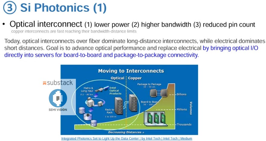
Traditionally, optical interconnects were deployed in metro networks and long-haul data transmission (0.1–89 km), connecting switches or data centers via fiber optics. Over the past decade, optical technology has moved deeper into the data center—rack-to-rack(1–100 m) interconnects are now commonly being replaced by optical links.
The diagram illustrates the envisioned trajectory:
Board-to-Board (50–100 cm)
Package-to-Package (10–50 cm)
These ranges were previously dominated by SerDes, retimers, and high-speed copper traces on PCBs. However, bandwidth efficiency and energy per bit have hit hard limits. Silicon photonics is the key to breaking through this barrier—bringing optical signaling into the motherboard, and even down to the chip packaging layer.
The Ultimate Goal of Optical I/O: Converging Photonics and Electronics
The long-term vision for optical I/O ismonolithic integrationorheterogeneous co-packagingof photonic transceivers with silicon logic platforms, enabling:
Package-to-Package Optical Links: Ultra-low-latency, energy-efficient communication channels between chiplets and high-speed modules.
Board-to-Board Optical Communications: Eliminating the energy losses and signal degradation associated with high-speed electrical SerDes.
Modular Internal Optical I/O: Optical PHYs that can support PCIe, CXL, Ethernet, and other protocols—enabling standardized, swappable interconnect modules.
Leading companies including Intel, NVIDIA, and TSMC are advancing this roadmap. Examples range from in-package SoIC optical modules, to fully integrated microring modulators, laser arrays, and photonic-electronic co-design platforms—clearly signaling a direct challenge to conventional copper-based architectures.
Bringing Light into Servers Is More Than Just Speed—It's Architectural Reinvention
Silicon photonics has evolved from being a backbone technology to becoming a system-level enabler. The interconnect paradigm for future servers and computing modules is shifting from copper-based to optical-first designs—delivering greater efficiency, scalability, and sustainability.

Co-Packaged Optics (CPO): The Future of Silicon Photonics and Switch Chip Integration
As AI, cloud computing, and hyperscale data centers drive explosive bandwidth demands, traditional electrical interconnects are hitting critical limits in both power consumption and bandwidth scalability. Co-Packaged Optics (CPO) has emerged as a transformative solution—an advanced heterogeneous integration approach that co-packages optical engines and logic chips (e.g., switch ASICs) on the same substrate. CPO delivers high bandwidth density, low power consumption, and superior signal integrity.
From Discrete Modules to Fully Integrated Optics
Traditional Architecture (Today):
Optical transceivers and switch ASICs are typically separate modules, connected via PCB traces and external retimer components. Data is routed electrically through optical I/O to the mainboard, resulting in:
Long electrical paths that introducesignal loss and crosstalk
Bulky external modulesthat consume valuable area and power
Complex signal timingand synchronization challenges
CPO Architecture (Future):
Optical modules are directly co-packaged with the ASIC die. Optical-electrical conversion occurs within the chip package using a silicon photonics engine, enabling ultra-short electrical paths, lower latency, and significantly improved energy efficiency. This architecture is ideally suited for next-gen 51.2 Tbps+ switches and AI infrastructure.
Key Elements in TSMC’s Heterogeneous Integration Platform
The diagram illustrates how a complete CPO solution involves multi-layered technological integration:
High-Performance Memory: Co-packaged or 3D stacked with logic dies to boost data buffering efficiency.
3D Stacking and SoIC: Enables both horizontal and vertical chiplet integration, scaling compute density.
Co-Packaged Optics: Integrates optical engines directly with switch ASICs, drastically reducing electrical-optical interconnect distances.
Silicon Photonics Engine: Includes microring modulators, photodetectors (PD), TIAs, and integrated lasers (e.g., EML or DFB), supporting multi-wavelength high-speed transmission.
Advanced Substrate, RDL, Interposer, and Integrated Voltage Regulators: Provide compact, low-noise power delivery and signal routing.
Core Benefits and Deployment Timeline of CPO
Benefits:
Bandwidth densityincreases by several fold to support Tbps-class switching.
Energy per bitis dramatically reduced, lowering cooling and power delivery costs.
Simplified module designand improved signal integrity enable tighter system integration.
Deployment Outlook:
According to recent roadmap disclosures from Broadcom, Intel, and NVIDIA, CPO is expected to enter large-scale commercial deployment beginning in 2025, targeting next-generation AI clusters, hyperscale switches, and HPC compute nodes. TSMC and its partners are actively maturing process capabilities in silicon photonics and advanced packaging, including COUPE, SoIC-X, and interposer-based integration.
CPO Brings Optics into Packaging—and Networking into the Chip
Co-Packaged Optics represents a system-level transformation. It brings optical signals from the network edge into the heart of the chip package and blurs the line between networking and compute. In the AI era, every bit of performance and energy efficiency counts. CPO will be the core optoelectronic engine powering the future of switches and data center architectures.

System-Level Management: Evolving from Functional Verification to Multidimensional Integration and Collaboration
As semiconductor design advances from nanometer-scale logic components to massive chiplet integration, heterogeneous die stacking, and system-in-package (SiP) architectures, single-dimensional verification is no longer sufficient to meet modern design complexity. System-Level Management is rapidly becoming a critical pillar in today’s and tomorrow’s chip development processes.
From Functional Correctness to Multidimensional Verification
In the 1980s, the central verification question was simple:“Is it functionally correct?”Designers focused on whether basic logic circuits worked as intended. But as circuits grew in scale and abstraction, the scope of verification evolved:
1980s (Transistor level): Functional verification only
1990s (Gate level): Function + timing verification (e.g., clock cycle performance)
2000s (ASIC era): Added power concerns (power estimation and simulation)
2010s (SoC design): Further included reliability analysis (aging, EM, TDDB)
Now: TheMore-than-Mooreera bringsheterogeneous integration challenges
The Shift to System-Level Verification in a Multiphysics World
As chip architectures move towardheterogeneous integration, designers face system-wide performance and reliability challenges across multiple physical domains—not just single-chip circuit behavior. In theSystem-Level Designera, verification must address a full range of interrelated dimensions:
Functional correctness
Timing closure
Power efficiency
Long-term reliability
Thermal integrity
Mechanical integrity(e.g., stress and deformation)
These factors interact with and influence each other. Verifying only at the module level may result in significant system-level failures, such as:
A functionally correct design throttled due to thermal bottlenecks
Undersized power delivery modules (VRMs) unable to meet peak demand
Micro-bump cracking from thermal expansion/contraction, causing signal instability
The Critical Challenge: Cross-Domain Integration and Concurrent Verification
Modern and future SoC designs must integrate:
Collaborative EDA toolchains(RTL, physical design, thermal, stress)
Co-simulation between packaging design and system-level modeling
Unified evaluation of chip + package + system + thermal performance
This system-level, co-optimized design and verification flow demands holistic thinking that spans silicon, packaging, mechanical, and system domains. It’s not just an engineering challenge—it represents a strategic threshold for competitive advantage in semiconductor innovation.
From “Will it run?” to “Will it break?”
Future semiconductor design is no longer just about verifying“Is this module logically correct?”— it now requires asking, much earlier in the process:
Can it operate within the specified power budget?
Will it maintain performance under varying temperatures?
Will the package withstand thermal cycling without failure?
Can the system function reliably across all real-world scenarios?
This shift marks not only a technological transformation in design verification, but also a broader industry transition toward a system-centric era of engineering integration.
System-Level Thermal Management: Overcoming Thermal Bottlenecks in 3D IC and BSPDN Designs
With the widespread adoption of advanced packaging and 3D IC technologies, thermal management has evolved from a passive consideration into a critical design factor in the early stages of development. Especially with the introduction of Backside Power Delivery Network (BSPDN) architectures, the thermal flow path, material thermal conductivity, and spatial power density distribution now have a profound impact on the overall thermal behavior of SoCs.
Non-Uniform Power Distribution and Hotspot Effects
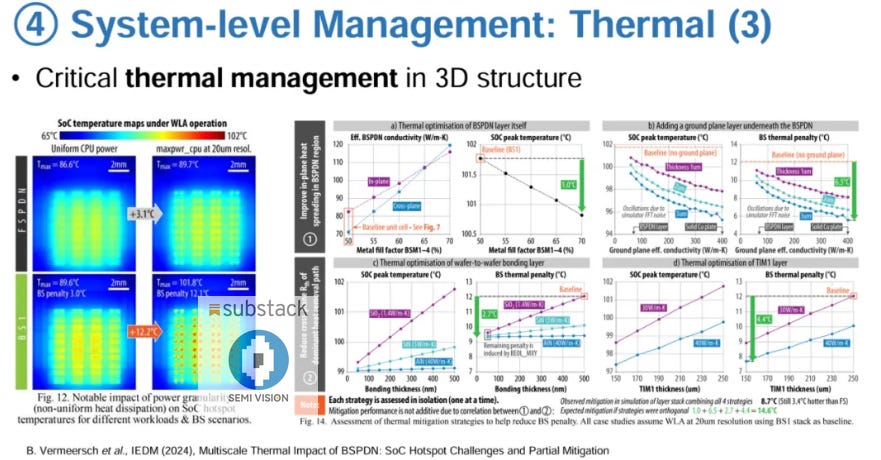
The figure on the left illustrates thermal maps of an SoC under different power distribution conditions:
Uniform Power Distribution: When CPU core power is evenly distributed, peak temperatures range from 86.6°C (in FSPDN architecture) to 89.6°C (in BSPDN), with relatively manageable thermal behavior.
Concentrated Power Distribution (20μm Hotspot Resolution): When power is concentrated in specific areas, the BSPDN design can reach temperatures as high as 101.8°C, with a BS penalty (Backside penalty) of +12.1°C, significantly increasing the risk of thermal failure and performance throttling.
This highlights that BSPDN can exacerbate thermal lag and local thermal resistance issues under power density fluctuations—especially in workload-level activity (WLA) scenarios—leading to potential instability in chip performance.
Multi-Level Thermal Management Strategies and Optimization Techniques
The diagram on the right presents various optimization methods to address BSPDN-related thermal bottlenecks, targeting improvements in the thermal conduction layer, metal fill density, grounding structure, and thermal interface materials (TIM):
(a) BSPDN Metal Fill Factor
Increasing metal fill density improves thermal conductivity (reducing peak temperature from 101.8°C to ~100.3°C).
Thermal conduction varies between in-plane and cross-plane directions.
Optimal design must consider the interaction between layout and heat diffusion direction.
(b) Ground Plane Layer
Adding a thermally conductive ground layer (e.g., Cu or AlN) beneath the BSPDN can significantly reduce both peak temperature and BS penalty.
With higher thermal conductivity and increased thickness, BS penalty can drop by up to 5.5°C.
Strategy involves careful material selection and thickness tuning.
(c) Wafer Bonding Thickness
Excessive wafer bonding layer thickness suppresses heat transfer.
Reducing bonding thickness from 500μm to 200μm lowers peak temperature from 101.8°C to 99.1°C, with a BS penalty improvement of 2.7°C.
The bonding method (e.g., Direct vs. Hybrid Bonding) also impacts thermal performance.
(d) TIM Thickness
The TIM layer bridges the package and heatsink, and its thickness significantly affects thermal resistance.
Reducing TIM thickness from 250μm to 170μm improves thermal conductivity and heat spreading uniformity.
A combined optimization of TIM and bonding strategy can reduce the BS penalty by 4.4°C.
Combined Strategy and Thermal Optimization Potential
By integrating all four strategies—thermal metal layer, ground plane, bonding thickness, and TIM optimization—up to 8.7°C of thermal improvement can be achieved (still 3.1°C higher than FSPDN), demonstrating that substantial thermal headroom remains in BSPDN designs.
It’s worth noting that the effects of these strategies arenon-additivedue to possible cross-interactions, requiring co-planning through advanced thermal simulations and system-level layout optimization.
From Power Delivery to Thermo-Mechanical Co-Design — A New Era for 3D IC Thermal Management
As chip design advances toward 3D integration and BSPDN architectures, thermal management becomes a design entry point, not just a packaging afterthought. Materials, stacking structure, power distribution, and bonding techniques must all be incorporated into early-stage multi-physics modeling and planning.
Only through end-to-end system-level co-integration—from architecture to packaging and thermal management—can high-performance 3D chips achieve breakthroughs in thermal reliability, stable performance, and sustained operation in high-power applications. This represents both a critical challenge and a strategic opportunity for advanced design teams in the AI era of SoC/HPC evolution.


PreviousNext
TopLatestDiscussions








See all