2025 VLSI – Paths Forward for CMOS Technology in the Ångström Era: Scaling Limits, 2D TMD Integration, Interconnect Challenges, and System-Level Co-Optimization
本頁目錄
- 2025 VLSI – Paths Forward for CMOS Technology in the Ångström Era: Scaling Limits, 2D TMD Integration, Interconnect Challenges, and System-Level Co-Optimization
- 2025 VLSI – Paths Forward for CMOS Technology in the Ångström Era: Scaling Limits, 2D TMD Integration, Interconnect Challenges, and System-Level Co-Optimization
2025 VLSI – Paths Forward for CMOS Technology in the Ångström Era: Scaling Limits, 2D TMD Integration, Interconnect Challenges, and System-Level Co-Optimization
- Source: SemiVision
- Author: SEMIVISION
- Published: 2025-07-01T14:23:10+08:00
- URL: https://tspasemiconductor.substack.com/p/2025-vlsi-paths-forward-for-cmos 2025 VLSI – Paths Forward for CMOS Technology in the Ångström Era: Scaling Limits, 2D TMD Integration, Interconnect Challenges, and System-Level Co-Optimization


2025 VLSI – Paths Forward for CMOS Technology in the Ångström Era: Scaling Limits, 2D TMD Integration, Interconnect Challenges, and System-Level Co-Optimization
Original Article by SemiVision Research (Samsung , TSMC, Nvidia , Lab 91)

Jul 01, 2025
∙ Paid


2025年6月30日
From Microns to Ångströms: Why Interconnection Defines the Future of CMOS
In his keynote speech at the IEEE VLSI Symposium,Keunhwi Cho, Vice President atSamsung Electronics, presented“Path Forward for CMOS Technology in the Angstrom Era — From Microns to Ångströms.”While the talk reflects on the historical evolution of CMOS scaling from the 0.18μm era, its core insight lies in howinterconnection—not just transistors—will shape the trajectory of system performance as we enter the Angstrom regime.
Beyond Scaling: A Shift from Process-Centric to System-Driven Innovation
As feature sizes shrink from microns to nanometers to Ångströms, the limitations of traditional transistor scaling have become apparent: short-channel effects, gate control challenges, material limitations, and power-performance tradeoffs. These challenges no longer reside purely at the device level—they have migrated to theinterconnect infrastructure, which now defines the boundaries of performance, efficiency, and system scalability.
Interconnection at the Heart of DTCO and STCO

Source: imec
As Cho emphasized, the complexity of AI-era chip design demands more than classic PPAC (Performance, Power, Area, Cost) metrics. The industry is rapidly embracing Design-Technology Co-Optimization (DTCO) and System-Technology Co-Optimization (STCO), where interconnects play a central role.
TSMC’s FinFlex technology and Samsung’s GAA (MBCFET) architecture exemplify innovations at the transistor level, but without dense, low-loss, high-bandwidth interconnects, their system-level benefits cannot be fully realized.
Enabling the Angstrom Era: Beyond Transistors—Interconnect is the Platform
Cho outlined Samsung’s future roadmap for integrating GAA technologies with advanced packaging and system integration, where interconnects are the enabler:
Backside Power Delivery (BSPDN) + Hybrid Bonding: Enhances power efficiency, reduces IR drop, and improves thermal paths while tightening interconnect density and reliability.
GAA + MRAM + HBM: Creates low-latency, logic-in-memory SoC platforms—enabled by high-density vertical and lateral interconnects.
Chiplet Architectures with 2.5D/3D Packaging: Requires ultra-high-density interconnects using CoWoS or FO-PLP platforms to ensure seamless modular integration.
High-Frequency Data Interconnects: As AI workloads demand explosive bandwidth, NRZ/PAM4 electrical interconnects and optical I/O technologies become indispensable.

2025年5月9日
CMOS Is Not Dead—Interconnect Drives Its Continued Evolution
While Moore’s Law may be slowing, CMOS is far from obsolete. As Cho concluded, the future of CMOS will not be defined by lithographic scaling alone, but by co-optimization across materials, device architectures, interconnects, and system packaging.
In the era of AI and HPC, interconnect is no longer a passive link—it is a first-class design element that governs power, performance, and scalability. From BSPDN to hybrid bonding, from GAA to co-packaged optics, the interconnect stack is the foundation upon which future semiconductor systems will be built
SemiVision’s latest article delves into the domain ofInterconnect Technologies, asserting that3D stackingmust rely oninterconnection via hybrid bondingfor its success.
At the IEEE IITC forum, one of the most respected conferences dedicated to advanced packaging technologies, a wealth of papers in 2025 extensively explore interconnection innovations. Proceedings clearly demonstrate the centrality of interconnect research to the future of chip integration .
Notably,Professor Kuan‑Neng Chen from NYCUhas authored multiple papers featuringback-side power delivery networks (BSPDN)analyses under thermal constraints, alongside studies on hybrid bonding techniques . His work underscores the critical role of coupling BSPDN with hybrid bonding to address heat dissipation and integration density issues.

2025年6月13日
Industry leaders such asApplied Materials (AMAT)andBesialso presented key contributions on hybrid bonding within wafer-to-wafer and die-to-wafer processes, demonstrating improvements in overlay accuracy and bonding yield .

SK hynixfeatured papers highlighting integration strategies to support futureHBM‑4 and HBM‑5memory stacks, tackling interconnect designs optimized for high‑bandwidth memory architectures.
Samsung Electronicsexplored scaling challenges in advanced node CFET and memory logic, including discussions of bonding-enabled connectivity for co-packaged optics and CFET interconnect structures.

Moreover,UNIST (Ulsan National Institute of Science and Technology)contributed several technical presentations at IITC 2025, reflecting South Korea’s strong presence in semiconductor interconnect research .
Why IITC 2025 Is Essential for Interconnect Technology
Comprehensive coverage of BEOL/MOL/chiplet bonding: IITC consistently focuses on advanced metallization, integration flows, and unit processes across interconnect domains .
Hybrid bonding as the enabler of future integration: As reviewed by Prof. Chen, hybrid bonding—metal-metal and dielectric-dielectric interfaces—is crucial for ultra-dense chiplet integration and improved thermal and performance characteristics .
BSPDN and hybrid bonding interplay: Research combining BSPDN network engineering with hybrid bonding improves both electrical power distribution and thermal management in 2nm‑node and beyond architectures.
Strong industry-academic collaboration: The conference brings together key voices from academia and industry giants such as IMEC, IBM, Samsung, SK hynix, AMAT, Besi, and UNIST to address system-level interconnect challenges .

2025年6月2日

2025年6月7日
IITC 2025 serves as a critical technical forum where expert speakers and industry researchers converge to address how 3D stacking depends on reliable and scalable interconnects. Through discussions on BSPDN, hybrid bonding, thermal dissipation, and high‑density memory integration, this conference anchors itself as an authoritative platform for the interconnect-driven future of semiconductor innovation.
As semiconductor manufacturing advances into the Ångström era, traditional silicon channels are reaching their physical scaling limits. Two-dimensional transition metal dichalcogenides (2D TMDs), such as MoS₂ and WSe₂, have emerged as promising candidates to extend CMOS scaling. With atomically thin bodies, excellent electrostatic control, and steep subthreshold slopes, TMDs are ideal for ultra-short gate lengths and are well-suited for next-generation device architectures like GAA and CFET.
While n-type TMD devices have already demonstrated impressive on-state performance, the development of high-performance p-type counterparts still faces challenges—particularly in contact resistance and threshold voltage tuning. Issues such as Schottky barriers at metal–TMD interfaces, material non-uniformities, and device variability continue to hinder large-scale adoption. Institutions like Intel and IMEC are working to address these hurdles by developing fully integrated process flows, including low-temperature deposition, nanoribbon stacking, gate dielectric engineering, doping, and contact optimization. Initial applications are expected in non-critical domains such as power management or I/O, serving as a transitional phase before integration into high-performance logic.
If these barriers can be overcome, 2D TMDs hold the potential to become key enablers for logic devices beyond the 1.4nm node. More than just a materials breakthrough, their adoption would signal a shift toward system-level co-optimization across device, process, and packaging domains—marking a new milestone in the post-Moore era of semiconductor innovation.

Lab 91is working on developing Transition Metal Dichalcogenide (TMD) based devices in various application domains, including optoelectronic/photonics. An example implementation maybe a monolithically integrated on-chip laser (replacing InP and associated complex packaging steps) or electro-optic SERDES, taking advantage of MoS2’s tunable bandgap (in monolayer form, it has a direct bandgap of 1.6 to 1.8 eV, which compares favorably to InP which has s direct bandgap of 1.3 eV)
For Paid Members ,SemiVision will discuss topics on
Next-Generation Interconnects in Logic Process Technology: From Dual-Damascene to 2D Material Integration
New Materials: Beyond Copper and Barriers
Structural Innovations: Air-Gaps and High Aspect Ratio Lines
Long-Term Strategy: 2D/1D Materials and Semi-Damascene
Co-Evolution of Process, Material, and Structure
Backside Power Delivery: A Key Technology to Solve Metal Congestion and Power Efficiency Challenges
The Era of Heterogeneous Integration: Chiplet Architectures and the Trillion-Transistor Leap
From N5 to A10: Process Shrink and Packaging Innovation in Tandem
Advanced Packaging and 3D IC: TSV and Hybrid Bonding Usher in a New Era of Heterogeneous Integration
Hybrid Bonding: A Breakthrough for Interconnect Density
Evolution of Packaging Platforms: From RDL to Interposer
3D IC: From Packaging Stacking to a Core Enabler of Performance and Power Efficiency
3D IC: Architectural Breakthrough Through Logic-Memory Partitioning
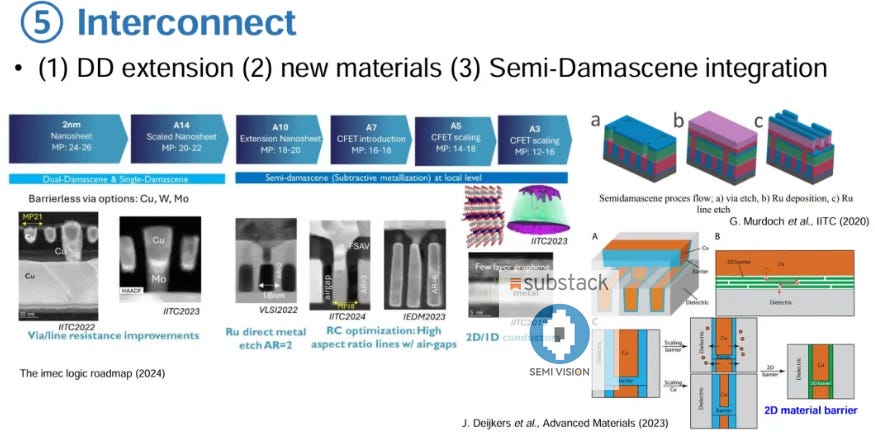
Next-Generation Interconnects in Logic Process Technology: From Dual-Damascene to 2D Material Integration
As logic nodes advance to 2nm and beyond—reaching A14, A10, A7, and even A3 generations—interconnects have become one of the most critical bottlenecks affecting power, speed, and reliability. To address these challenges, the semiconductor industry is focusing on three major directions: extending dual-damascene (DD) processes, introducing new materials, and adopting semi-damascene integration.
Traditionally, dual-damascene (DD) structures have been widely implemented in the back-end-of-line (BEOL) process. However, as metal pitch shrinks to 20nm and even down to 12nm, DD architectures face serious issues such as line-to-line spacing limitations, increased RC delay, and excessive barrier layer volume, prompting the search for more advanced interconnect schemes.
New Materials: Beyond Copper and Barriers
To reduce total resistance in vias and metal lines, barrier-free via technology is gaining traction. Conventional Cu interconnects require diffusion barriers (e.g., Ta/TaN), which introduce high resistivity and consume valuable space. To overcome this, researchers are exploring direct deposition of barrierless via metals such as Cu, W, and Mo. For instance, contact structures with metal pitch at 21nm have demonstrated ultra-low resistance and significant improvements in RC delay and power consumption.
Among new materials, ruthenium (Ru) has emerged as a leading candidate to replace Cu due to its excellent conductivity and electromigration resistance. Recent studies have demonstrated direct Ru deposition and high aspect ratio structures (~2:1), often combined with Self-Aligned Via (SAV) and advanced barrier engineering. However, chemical mechanical planarization (CMP) for Ru remains a major challenge, as most current CMP technologies are optimized for Cu and W.
Structural Innovations: Air-Gaps and High Aspect Ratio Lines
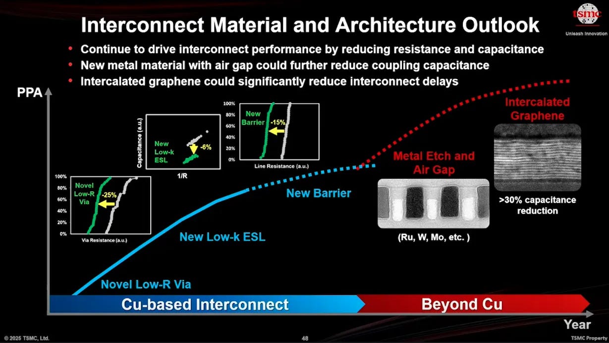
Structural innovations such asair-gap integrationandhigh-aspect-ratio (AR > 6) interconnectshelp reduce parasitic capacitance and crosstalk—critical to achieving high-speed, low-power logic. Leading manufacturers such as IMEC, Intel, and TSMC have introduced air-gap structures in their upper metal layers and continue to optimize process uniformity and long-term reliability.
Air-Gaps and High Aspect Ratio Interconnects: Structural Innovations for the Ångström Era
As transistor scaling approaches the Ångström era, traditional limitations of interconnects—particularly parasitic capacitance, resistance, and crosstalk—are becoming critical bottlenecks. To meet the demands of high-speed, low-power logic, the industry is turning to structural innovations such asair-gap integrationandhigh aspect ratio (AR > 6) metal lines. These techniques are transforming backend-of-line (BEOL) design, enabling both performance gains and new challenges in materials, thermal management, and process integration.
- Why Air-Gaps Matter
Air has the lowest possible dielectric constant (close to 1), making it an ideal insulator between metal lines. By replacing traditional low-k materials or SiO₂ with selectively formed air gaps, engineers can drastically reduce line-to-line capacitance. Studies have shown that air-gap integration can reduce parasitic capacitance by up to 39%, and in extended structures—where gaps also form between interlayer regions—reductions can reach 49%. This translates directly into lower RC delay and reduced dynamic power, both essential for advanced logic performance.
- High Aspect Ratio Lines and Their Synergy with Air-Gaps
Research from IMEC has demonstrated that with AR exceeding 6:1, interconnect performance improves significantly. When combined with ruthenium (Ru) or other advanced conductors, high AR lines become even more attractive for next-generation logic nodes beyond 2nm.
- IMEC’s Advanced Integration Schemes
IMEC has pioneered several experimental platforms involvingsemi-damascene Ru interconnects with self-aligned vias and integrated air-gaps. These structures, implemented at 18nm metal pitch, have shown strong potential for low-resistance, low-capacitance performance while maintaining compatibility with high-volume manufacturing flows. Notably, these processes often eliminate the need for chemical-mechanical polishing (CMP), simplifying integration.
IMEC has also explored the use ofintermetallic materialssuch as AlCu and Al₂Cu, which offer lower resistivity and improved reliability when paired with air-gap schemes. These hybrid approaches are seen as candidates for the sub-1nm node, where both electrical performance and structural integrity must be preserved under extreme scaling.
Imec Shows Path to Line Resistance Halving using Semi-Damascene with High-Aspect-Ratio Processing
- Industry Adoption: Intel, TSMC, and Samsung
Intel was among the first to deploy air-gap structures in high-performance metal layers starting from its 14nm node. Their published data demonstrated RC delay improvements of 14–17% for wire pitches between 80–160nm. Intel has since explored more advanced subtractive Ru processes with self-forming air-gaps, targeting 25nm and below pitch applications with over 25% capacitance reductions.
Major foundries such as TSMC, Samsung, and IBM are actively exploring similar integrations using new conductor materials and self-aligned air-gap processes. Samsung and IBM, in particular, have shown interest in ruthenium-based lines with high AR and integrated gaps for performance-critical metal levels in HPC and AI accelerators.
- Reliability and Integration Challenges
Despite the clear performance benefits, air-gap structures introduce new reliability and process control issues. Thethermal conductivity of air is extremely low, raising concerns about localized heating and electromigration. Studies estimate that localized temperature increases may reach 15–20%, especially in stacked or dense layouts.
Moreover, the fabrication of air-gaps requirescomplex process flows, typically involving the deposition of sacrificial polymers, selective etching, and careful encapsulation to avoid moisture ingress or mechanical collapse. The introduction of semi-damascene integration flows helps address some of these issues by improving line definition and via alignment, but full-volume reliability qualification remains ongoing.
- Outlook and Strategic Impact
As the semiconductor industry enters the Ångström regime, solving interconnect bottlenecks becomes as important as transistor innovation. Air-gap structures and high AR interconnects represent a powerful strategy to reduce parasitic effects and enable higher clock speeds without compromising power budgets.
The convergence of these structural techniques with new materials—such as ruthenium, molybdenum, and intermetallics—will likely define the roadmap for 1nm and beyond. Integration with advanced packaging, power delivery networks, and thermal management systems will be key to unleashing their full potential.
In the era of AI and massive chip-scale systems, interconnects are no longer just passive wires. They are critical enablers of system performance, and air-gap technology may well become the silent hero of the next wave of semiconductor breakthroughs.
Long-Term Strategy: 2D/1D Materials and Semi-Damascene
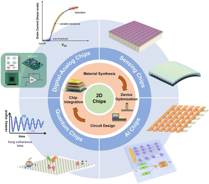
In the long-term roadmap, 1D and 2D materials such as graphene and carbon nanotubes are under active investigation due to their superior conductivity and atomically thin profiles, offering potential solutions for ultra-scaled interconnects. These materials may serve both as conductors and as diffusion barriers, helping reduce interconnect volume, resistance, and electromigration risks.
Semi-damascene integration is also emerging as a promising solution for local interconnects, particularly in lower metal layers (Metal 0/1). Unlike conventional damascene, semi-damascene uses a subtractive process flow: via-first → metal deposition → patterning, which enables better control over metal morphology and interfaces. This method offers advantages in yield, electrical uniformity, and metal density control, making it ideal for dense logic integration.
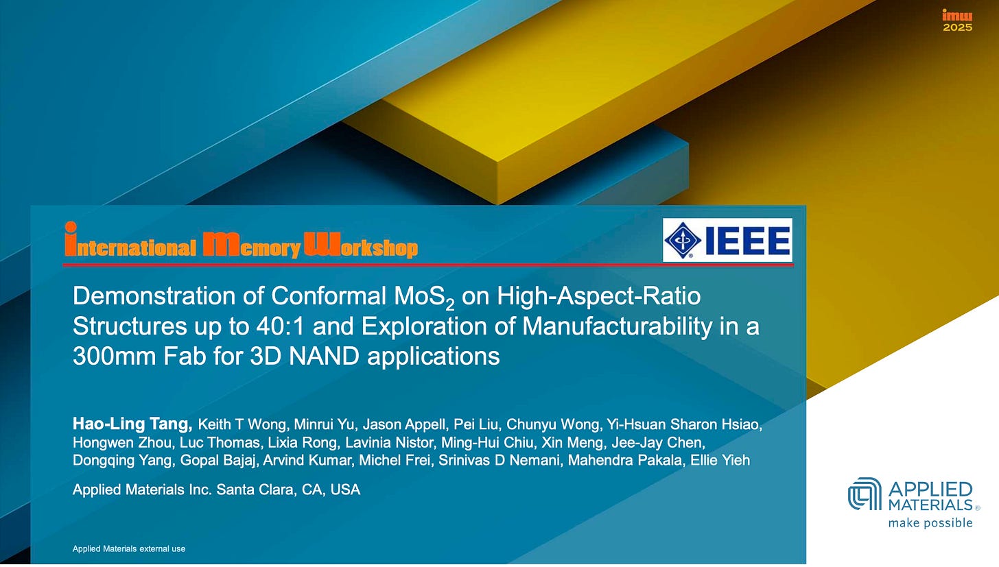
Another growing area is the use of 2D materials as diffusion barriers. Traditional barriers consume a disproportionate amount of space at scaled dimensions, degrading RC performance. In contrast, 2D atomic-layer materials (e.g., graphene, MoS₂) can block metal diffusion with minimal impact on resistance and footprint. Experimental results have demonstrated excellent thermal stability and barrier performance even at 10nm metal pitch.
Co-Evolution of Process, Material, and Structure
In summary, the evolution of logic interconnects will hinge on the synergistic advancement of three pillars:
Process architecture innovationssuch as semi-damascene,
New conductive and barrier materials(e.g., Ru, Mo, 2D materials),
Physical optimizationsincluding high-AR lines and air gaps.
Only through concurrent breakthroughs in these domains can logic chips maintain the delicate balance of power, speed, and reliability in the deeply scaled nodes—paving the way for the next generation of AI and high-performance computing (HPC).
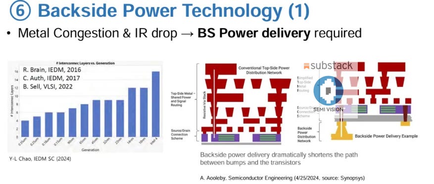
Backside Power Delivery: A Key Technology to Solve Metal Congestion and Power Efficiency Challenges
As process nodes advance below 5nm, interconnect structures in chips are facing unprecedented challenges. One of the most critical issues ismetal congestionandIR drop (voltage loss)caused by the rapidly increasing number of metal layers. According to multiple statistics from IEDM and VLSI, the number of metal layers has increased from about 4 layers during the 0.35μm era to more than 14 layers at the 5nm node—and is expected to exceed 16 layers below 3nm.
This evolution has led top metal layers to not only handle high-speed signal transmission but also deliver substantial power, exacerbating routing congestion, complicating power management, and introducing timing uncertainty. In response, Backside Power Delivery (BS-PDN) is emerging as a revolutionary architecture in advanced logic design.
In traditional Top-Side Power Delivery systems, power must enter from the top-side bump and traverse through multiple metal layers and vias to reach the transistor layer. This results in long power delivery paths, significant IR drop, and shared routing layers between power and signals—further limiting signal integration and layout efficiency.
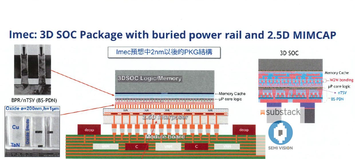
In contrast,Backside Power Deliveryrelocates the power delivery network (PDN) to the backside of the chip, using through-silicon vias (e.g., Power TSVs or similar vertical contacts) to directly supply power near the source/drain region. This architecture offers multiple advantages:
Shorter power paths, significantly reducing IR drop and improving overall power efficiency and transient response.
Freeing up top metal layers, allowing them to be used for signal routing, thus enhancing signal integration density.
Simplifying upper-layer design, reducing metal layer count and process complexity while mitigating RLC effects that cause signal delay and crosstalk.
The structural diagram clearly illustrates the difference: in traditional designs, the red area represents mixed power and signal layers in the top metal stack, which are not only complex but also susceptible to process variation and thermal stress. Under a backside power architecture, power routing (shown in red) is moved to the bottom, dedicated solely to power delivery, creating clearpower/signal decouplingand reducing interference from interlayer routing crossover.
Currently, Intel has implemented a backside power architecture calledPowerViain its 20A/18A nodes as part of its RibbonFET era. TSMC and Samsung also have respective BS-PDN roadmaps, underscoring the growing importance of backside power in advanced logic platforms.
Backside Power Delivery is transitioning from research to real-world implementation and is expected to become a foundational technology for logic platforms below 2nm. By addressing metal congestion, IR drop, and routing limitations, BS-PDN is a critical innovation for continuing Moore’s Law and supporting the growing design complexity of AI and high-performance computing. In the future, when combined with chip stacking, chiplet integration, and heterogeneous packaging, its system-level benefits will become even more significant.

The Era of Heterogeneous Integration: Chiplet Architectures and the Trillion-Transistor Leap
As advanced semiconductor nodes move below 3nm, traditional monolithic chip designs are reaching physical and manufacturing limits. Under the growing challenges of yield, cost, thermal design, and scalability,heterogeneous integrationhas rapidly emerged as a core enabler for next-generation AI and high-performance computing (HPC) platforms.
The evolution of heterogeneous integration can be summarized in three key directions:chiplet modularization, multi-function integration, and diverse customization. These strategies enable system-level designs that are no longer constrained by single-die size or yield. Instead, multiple dies with different functionalities (logic, memory, I/O, AI accelerators) are integrated into a unified platform via advanced packaging techniques likeCoWoS, InFO, and SoIC, providing greater scalability and flexibility.
From N5 to A10: Process Shrink and Packaging Innovation in Tandem
As shown in the timeline, since the 5nm (N5/N4) era began in 2020, the industry has simultaneously pushed forward both process miniaturization and packaging innovation. With continued progression through N3, N2, A14, and A10 nodes, chip integration strategies have evolved from monolithic designs to3D chiplet-based architectures, enabling designs with over100 billion (100B) to 1 trillion (1T) transistors.
3D heterogeneous integration allows engineers to optimize each sub-module with the most suitable process node—for example, using cutting-edge GAA nodes for compute logic, mature nodes for SRAM or HBM, and cost-effective nodes for I/O or PHY—thereby improving overallPPAC (Performance, Power, Area, Cost)efficiency.
Realizing the Trillion-Transistor Era: NVIDIA Blackwell Hits 208B
NVIDIA's new Blackwell GPU platform exemplifies the power of heterogeneous integration. It features a staggering 208 billion transistors and achieves 20,000 TFLOPS of single-precision performance—far surpassing the previous Hopper H100 (80B, 4000 TFLOPS) in both compute density and energy efficiency.

Comparing GPU generations from NVIDIA since 2016:
Pascal (2016): 15.3B transistors, 19 TFLOPS
Volta (2017): 21.1B, 130 TFLOPS
Ampere (2020): 54.2B, 620 TFLOPS
Hopper (2022): 80B, 4000 TFLOPS
Blackwell (2024): 208B, 20,000 TFLOPS
In just eight years, both transistor count and compute performance have grown by orders of magnitude—demonstrating that chip innovation is no longer solely driven by process scaling, but increasingly by architectural and packaging breakthroughs.
Industry Implications and Future Outlook for Heterogeneous Integration
Heterogeneous integration is not just a technical breakthrough; it marks a paradigm shift for the semiconductor industry. As AI models exceed 1 trillion parameters and data/bandwidth demands explode, monolithic SoCs can no longer meet performance and scalability needs.
Chiplet architectures offer flexible composition of IP blocks, memory modules, and compute engines, allowing customization for inference, training, edge, or data center scenarios. This also reduces design reuse complexity, accelerates testing, and shortens time-to-market.
On a technical level, heterogeneous integration is accelerating the adoption of enabling technologies such as TSV, SoIC, 2.5D/3D IC packaging, optical interconnects, and backside power delivery (BSPDN)—paving the way for “More than Moore” era innovation.
Heterogeneous integration is moving from research to mainstream AI chip design practice. Through chiplets, 3D packaging, and cross-node integration, it not only enhances performance and scalability, but also lays the hardware foundation for ultra-large AI models and next-generation data centers.
Looking ahead, we will see more “System-in-Package” (SiP) design philosophies that drive the semiconductor industry into the true era of trillion-transistor integration.
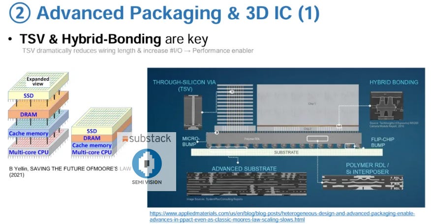
Advanced Packaging and 3D IC: TSV and Hybrid Bonding Usher in a New Era of Heterogeneous Integration
As traditional process scaling approaches physical limits, the semiconductor industry is rapidly shifting its focus to packaging-level innovations to continue Moore’s Law. Among these, 3D Integrated Circuits (3D ICs) and advanced packaging technologies have become critical for integrating logic and memory systems. Two core pillars driving this transformation are Through-Silicon Via (TSV) and Hybrid Bonding.
3D Heterogeneous Integration: Vertical Integration Across Functional Blocks
Heterogeneous integration is not only an extension of process scaling—it is also the foundation for a“System-in-Package (SiP)”paradigm. The diagram illustrates a typical 3D stack system, vertically integrating multiple functional layers such as CPU cores, cache memory, DRAM, and even SSD storage. This vertical stacking enables the creation of high-performance, high-bandwidth computing platforms.
The key advantage of this structure lies inshortening signal transmission paths,boosting data throughput, andreducing power consumption, making it especially valuable in AI, HPC, memory stacking, and edge computing applications.
TSV: Enabling High-Speed Vertical Interconnects
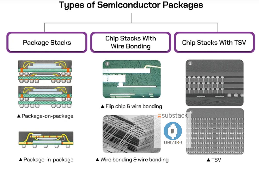
Source: SK Hynix
Through-Silicon Via (TSV)technology allows signals and power to penetrate vertically through the silicon die, replacing traditional long lateral interconnects routed through the package substrate. The benefits include:
Shorter interconnect paths: Significantly reduces latency and power consumption.
Higher I/O density: Supports more communication channels, ideal for high-speed memory like DRAM or HBM.
Enhanced 3D packaging scalability: Enables deeper stacking and tighter integration across layers.
TSV is the foundational technology for high-speed DRAM packaging (e.g., HBM) and is widely used in dense logic modules and edge computing platforms.
Hybrid Bonding: A Breakthrough for Interconnect Density

Complementing TSV, Hybrid Bonding combines copper-to-copper (Cu-Cu) and oxide-to-oxide bonding to achieve:
Ultra-high interconnect density: Interconnect pitch as low as 1–3 µm, far exceeding traditional flip-chip bump pitches.
Low contact resistance: Enables high-speed, low-power signal transmission, ideal for high-performance logic and memory.
Precise alignment capability: Supports die-to-die and wafer-to-wafer stacking with high accuracy.
Hybrid bonding has become a foundational technology for modern high-end packaging platforms like TSMC’s SoIC and Intel’s Foveros, transitioning from bump-based assembly to bump-less direct bonding.

2025年1月20日
Evolution of Packaging Platforms: From RDL to Interposer
To support TSV and hybrid bonding, advanced packaging platforms are evolving in parallel:
Polymer RDL (Redistribution Layers): Provide fine-line routing, widely used in fan-out packaging.
Silicon Interposer: Offers flat surfaces and multi-layer metal routing for high-speed chip integration (e.g., CoWoS).
Advanced Substrate: Enables multi-die stacking and ultra-wide bandwidth interfaces, crucial for chiplet-based systems.
These structures elevate packaging from a passive post-fabrication step to a primary enabler of system-level performance, power, and area optimization.
TSV provides the foundational vertical interconnects for 3D ICs, while Hybrid Bonding pushes the limits of interconnect density and signal integrity. Together, they enable the high-integration demands of AI, HPC, and next-generation SoC designs. As Moore’s Law scaling slows, these advanced packaging technologies are redefining semiconductor innovation—ushering in an era where “packaging is the system” and “packaging is performance.”
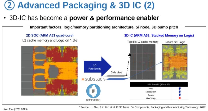
3D IC: From Packaging Stacking to a Core Enabler of Performance and Power Efficiency
As chip complexity and die sizes increase, traditional 2D SoC designs are hitting limitations in performance, power, and area (PPA). Today, 3D Integrated Circuit (3D IC) technology—once seen as a supplementary path to extend Moore’s Law—has evolved into a proactive enabler of system-level performance and energy efficiency.
The diagram compares two designs based on the same ARM Cortex-A53 quad-core architecture: the left shows a traditional 2D SoC layout, while the right illustrates a 3D IC implementation using stacked dies.
Traditional 2D SoC: Flat Design Limitations
In a 2D SoC, logic and L2 cache are implemented on the same silicon die, leading to several challenges:
Cache occupies large die area, limiting available space and routing resources for logic.
All communication happenshorizontally, increasingsignal delay and energy loss.
Power delivery and thermal dissipationare confined to the top plane, restricting scalability and performance headroom.
While sufficient for past generations, this flat design approach falls short in the face of modern AI, HPC, and other high-bandwidth, high-power applications.
3D IC: Architectural Breakthrough Through Logic-Memory Partitioning
In the 3D architecture, designers can vertically partition L2 cache onto a separate top die, stacked above the logic bottom die. This 3D partitioning brings notable advantages:
Significant area reduction: Logic and memory are decoupled spatially, easing 2D layout constraints.
Much shorter data paths: Direct vertical links viaTSVs or Hybrid Bondingminimize latency and power.
Process flexibility: Logic and memory can use different process nodes, supportingheterogeneous integration.
Higher packaging density: Enables compact integration for AI, edge, and HPC platforms.
PPA Gains: 3D vs. 2D – Quantified Benefits
Experimental data in the diagram clearly shows how 3D ICs outperform traditional 2D SoCs across key metrics:
Area: Reduced – results in a more compact die.
Performance: Increased – thanks to faster data access and lower interconnect delay.
Power: Lower – resulting in betterperformance-per-watt.
Max temperature: Slightly higher, but manageable through thermal-aware packaging techniques.
These results highlight that 3D IC is not just about adding a layer, but rather re-architecting systems for balance across power, performance, and area.
3D IC as the Engine of Future Computing Platforms
Source: Systems Design Lab
The core value of 3D IC lies in breaking the 2D scaling bottleneck through layered logic-memory design and advanced packaging techniques like TSV and Hybrid Bonding. It enables true system-level performance optimization.
This makes 3D IC architectures especially suited for high-speed, memory-intensive applications such as AI inference and training, high-bandwidth data access, and next-generation communication platforms—positioning them as a foundational pillar in the future of chip design and semiconductor manufacturing.
While 3D stacking offers significant gains in performance and bandwidth, it also introduces severe thermal challenges due to the high power density and compact vertical integration of multiple dies. To address this bottleneck, TSMC has developed an innovative liquid cooling architecture called theSi-Integrated Micro-Cooler (IMC-Si). This system incorporates microfluidic cooling channels directly into the silicon interposer used in CoWoS (Chip-on-Wafer-on-Substrate) packaging, enabling efficient thermal management for power densities exceeding2.5 W/mm².

In one test configuration, the IMC-Si system was applied to a package containingfour SoC dies and six HBM stacks. By circulating40°C water at a flow rate of approximately 10 liters per minute, the system was able to dissipate over3000 wattsof total power—demonstrating its effectiveness in handling high-performance AI workloads.
The implementation process of the Si-Integrated Cooler involves several key steps:
First, a protective layer is applied during the packaging process, followed by die flip and C4 bump bonding. After removing the protective layer,elastic sealing compoundsare applied to mitigate warpage risks. Finally, aliquid manifold systemis installed to evenly distribute coolant across multiple dies, ensuring uniform thermal flow and efficient heat extraction throughout the 3D package.
With its high thermal efficiency and integration compatibility, TSMC’s IMC-Si is emerging as a critical enabler for next-generation, high-power AI computing platforms.

2025年6月2日

2025年5月30日

2025年6月27日


PreviousNext
TopLatestDiscussions








See all