NVIDIA x TSMC: A Milestone in Silicon Photonics and Optical Integration
NVIDIA x TSMC: A Milestone in Silicon Photonics and Optical Integration
- Source: SemiVision
- Author: SEMIVISION
- Published: 2025-03-28T09:18:27+08:00
- URL: https://tspasemiconductor.substack.com/p/nvidia-x-tsmc-a-milestone-in-silicon (1) NVIDIA x TSMC: A Milestone in Silicon Photonics and Optical Integration


NVIDIA x TSMC: A Milestone in Silicon Photonics and Optical Integration
Original Articles by SemiVision Research

Mar 28, 2025
∙ Paid
Before reading this article, we recommend referring to SemiVision Research’s previous coverage on NVIDIA’s silicon photonics and Co-Packaged Optics (CPO) for additional context.

Drive Into Nvidia CPO Based Switch
IEDM 2024: TSMC Silicon Photonics Advancements
TSMC Optical Chiplet Integration and CPO Platform: EPIC-BOE

EPIC=Eletrobic-Photonic chiplet Integration Technology with IC Process
BOE=BroadBand Optical Engine
Future GAI systems require much higher parallelism than current architectures, alongside greater energy efficiency, bandwidth density, and lower latency. TSMC proposes EPIC-BOE, a fully integrated technology platform designed for broadband optical engine (BOE) applications. This system enables chip-to-fiber-to-CoWoS level integration and uses TSMC’s 3DFabric and IC process technologies to achieve compact co-packaged optics (CPO), optimizing the PPA (power, performance, area) metrics for GAI systems.
The composition of an Optical Engine (OE) requires two types of dies: the Photonic Integrated Circuit (PIC) and the Electronic Integrated Circuit (EIC), which are fundamentally related to electro-optical conversion.
TSMC, traditionally focused on logic chips — essentially the EIC part — is now actively expanding into the photonics domain, where the PIC component dominates. Recognizing the importance of integrating both photonic and electronic subsystems, TSMC has introduced theCOUPEplatform and theiOIS(Integrated Optical Interconnection System) platform to bridge these two worlds.
Ultimately, by integrating the entire system from chip to fiber to CoWoS level, TSMC has redefined its silicon photonics strategy with the EPIC-BOE platform — a new benchmark for scalable, high-performance optoelectronic integration.
EPIC-BOE supports a wide bandwidth range from 1260 to 1360 nm and integrates vertical couplers capable of supporting high fiber counts. Unlike traditional edge couplers (EC), which are limited by edge warping when integrating 40–80 fibers per row, EPIC-BOE's vertical coupling design eliminates such limitations and allows for multi-row integration.
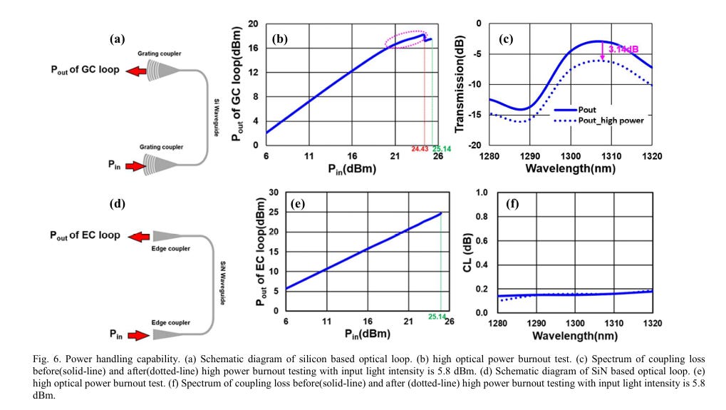
The process uses IC-based techniques to implement SiN waveguides, optical couplers, interlayer transitions, and polarization control devices. The waveguide propagation loss is 0.01 dB/cm, with a 90-degree bend loss of just 0.001 dB per turn. The vertical coupler achieves ultra-low coupling loss (0.08 dB) and can sustain high-power laser input (300 mW for 3 hours) without degradation. Interlayer transition loss is 0.015 dB. The polarization diversity PBSR achieves an extinction ratio of 23 dB and 0.3 dB loss across TE/TM modes, enabling compact integration in FAUs.
TSMC is about to publish a new paper highlighting the advantages of SiN waveguides (SiN WG) and their integration into TSMC’s silicon photonics platform.
Photonics Platform Integration
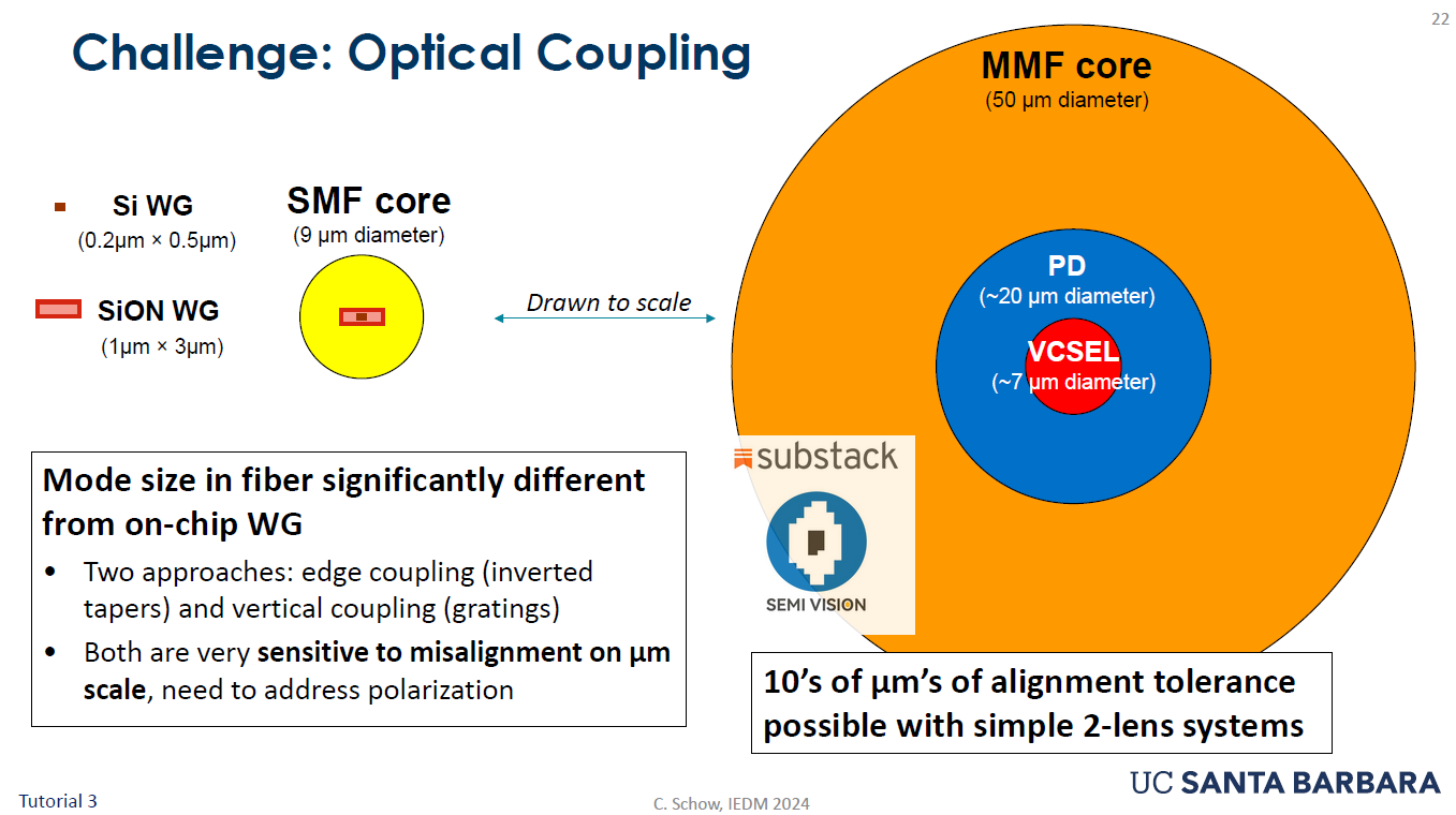
Silicon photonics is transforming integrated optics by enabling scalable, manufacturable optical circuits. Optical coupling—especially from fiber to chip—is a key challenge. Common coupling types are grating couplers (GCs) and edge couplers (ECs). While GCs offer easy alignment for fiber arrays, they suffer from limitations in angle sensitivity, polarization dependence, and bandwidth. ECs, on the other hand, offer better broadband performance but struggle with scaling to multiple fiber rows due to chip edge limitations.
Vertical couplers, as adopted by EPIC-BOE, provide a breakthrough in achieving scalability across fiber count per row, number of rows, and individual fiber bandwidth. The system combines COUPE (platform for photonic engines), COIT (complementary optical interconnect top layer), and iFAU (integrated fiber array unit) to provide broadband, vertically-coupled, multi-row optical I/O.


COUPE (platform for photonic engines)
COIT (complementary optical interconnect top layer)
iFAU (integrated fiber array unit)
iOIS (Intergrated to Advanced Package)
Silicon Photonic Supply chain by SemiVision Research
Keep updated latest information to our Paid Members
Taiwan Silicon Photonic Ecosystem
UMC Silicon Photonic Ecosystem
Global Silicon Photonic Ecosystem
Marvell Silicon Photonic Ecosystem
Broadcom Silicon Photonic Ecosystem
For Paid Members , SemiVision Research will discuss following topics:
Why Is NVIDIA Pushing for CPO Switches? Start with Why
Why Choose CPO Technology?
Technical Architecture of the CPO Switch
An in-depth study of the optical engine design approaches by TSMC and NVIDIA
Introduction to the Key Features of TSMC’s EPIC-BOE Platform
Broadcom vs. NVIDIA: A Comparison of CPO Switch Strategies
Why Is NVIDIA Advancing Micro-Ring Modulators and CPO Technology?


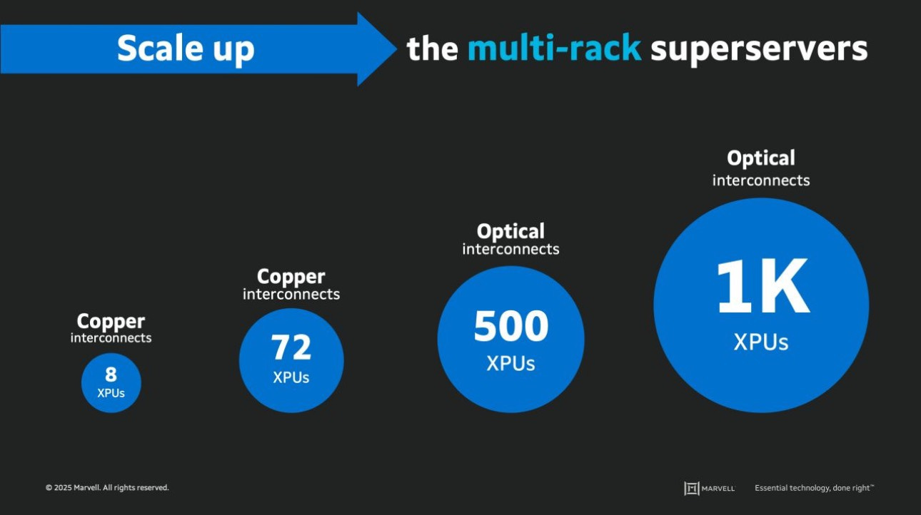
In the architecture of AI Clusters, Scale Out plays a critical role. As a result, Co-Packaged Optics (CPO) technology is destined to become a key development focus. At the same time, with the growing demand for higher-performance GPUs and XPUs, lower latency, and faster data movement, the evolution of AI interconnects is becoming mission-critical.
Scale-up networks are moving beyond traditional copper, transitioning to integrated optics to improve efficiency and speed.
Scale-out networks require resilient, high-bandwidth connectivity to support massive AI clusters.
Silicon photonics innovations are paving the way for CPO technology and next-generation DSPs (Digital Signal Processors), enabling AI infrastructure to scale smarter and faster.
Why Is NVIDIA Pushing for CPO Switches? Start with Why
At the 2025 GTC Conference, NVIDIA CEO Jensen Huang presented a simple yet striking calculation:
In a typical three-tier data center network architecture, each GPU requires six optical modules. Assuming each traditional optical module consumes around 30W and has an energy efficiency of 18.75 pJ/bit, an AI data center equipped with one million GPUs would require six million optical modules, resulting in a total power consumption of 180 megawatts.
In contrast, by adopting CPO (Co-Packaged Optics), the power consumption per port drops to 9W, with an improved energy efficiency of 5.63 pJ/bit. The total power consumed by optical engines can be reduced to 54 megawatts, achieving a 30% reduction—a figure consistent with data published by Broadcom.
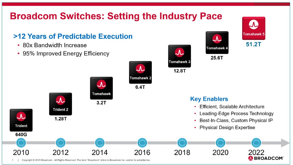
To put that into perspective, the saved power is enough to operate 126,000unitsof NVIDIA’s B200 GPUs, each rated at 1kW. This is the core reason behind NVIDIA’s commitment to advancing CPO technology.
The CPO (Co-Packaged Optics) solutions adopted by Broadcom and Nvidia feature different PIC (Photonic Integrated Circuit) and EIC (Electronic Integrated Circuit) packaging methods and specifications. In the CPO industry, each solution is treated as a case-by-case study, tailored to meet specific requirements.
To address the challenges of power consumption, TSMC and NVIDIA have launched a joint initiative in silicon photonics and Co-Packaged Optics (CPO).
Much like what TSMC presented at IEDM 2024, the technologies and architectures bear a striking resemblance to NVIDIA’s Quantum X platform.
SemiVisionResearch will gradually guide the audience through a detailed analysis of TSMC’s papers, exploring how these innovations can be directly applied to NVIDIA’s Quantum X system.
Why Choose CPO Technology?
The core idea behind CPO (Co-Packaged Optics) is to place the switch chip and the optical engine within the same package. This significantly reduces the physical distance between them, thereby minimizing signal path loss, eliminating the need for DSP-based signal compensation, and ultimately lowering both power consumption and cost.
• Traditional electrical interconnects can suffer up to 22 dB of signal loss.
• With CPO, the link loss is reduced to just 4 dB, improving signal integrity by 18 dB—a significant enhancement.
Technical Architecture of the CPO Switch
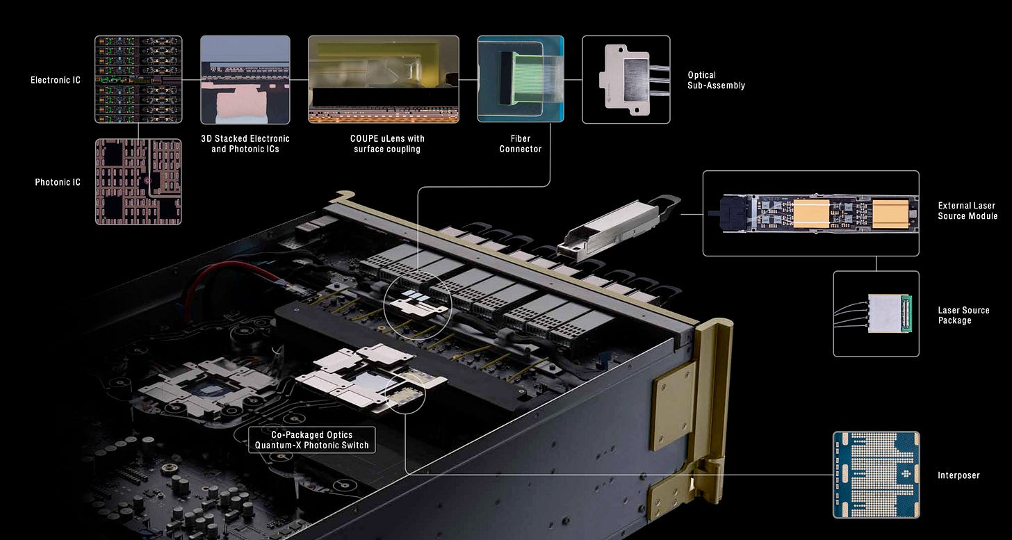

NVIDIA’s CPO system integrates multiple cutting-edge technologies, including:
•EIC (Electronic Integrated Circuit)
•PIC (Photonic Integrated Circuit)
•3D packaging with PIC and EIC
•COUPE uLens with surface coupling
•Externally pluggable laser modules(8 laser diodes per module)
•MPO-12 fiber connectors, with144 portstotaling1,152 optical fibers
The optical engine adopts a single-wavelength Micro Ring Modulator (MRM) design, with each channel operating at 200 Gbps.
Each optical engine contains 8 channels (totaling 1.6 Tbps).
Three optical engines form one module, and each switch chip is configured with six modules—resulting in a total bandwidth of 28.8 Tbps per switch.
The full CPO switch includes four switch chips, delivering an aggregate bandwidth of 115.2 Tbps, and utilizes liquid cooling for thermal management.
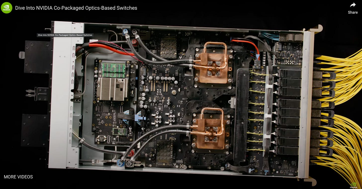
An in-depth study of the optical engine design approaches by TSMC and NVIDIA
TSMC’s silicon photonic platform adopts a micro-ring-based design
Why Not Use a Multi-Wavelength Design?
NVIDIA has chosen a single-wavelength architecture, in contrast to Broadcom’s MZM-based multi-wavelength approach. The primary reason lies in the requirements of high-radix applications, which enable the construction of larger-scale networks and help reduce overall costs.
Whether NVIDIA will introduce a multi-wavelength version in the future remains to be seen and will largely depend on market demand.
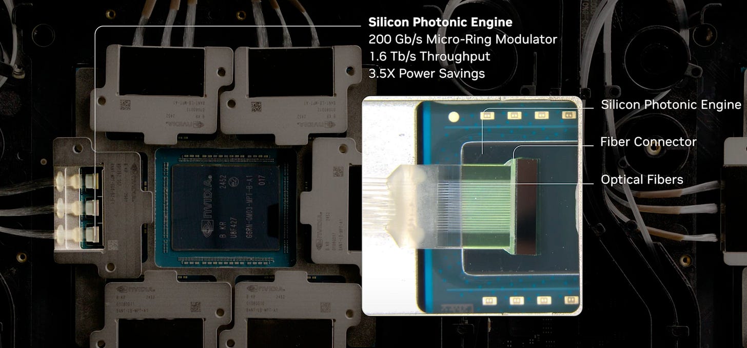
Optical Coupling Scheme and Packaging Design
The COUPE platform supports vertically incident light, which is then deflected horizontally via a prism, aligning with the fiber array unit (FAU). This design is consistent with descriptions presented in TSMC’s IEDM publications.
Optical coupling is very important for fiber to optical I/O parts, at presentation included only one image labeled "COUPE ulens with surface coupling."
In the image, a prism with a reflective slope and a fiber array (FA) socket can be clearly seen. The prism redirects light emitted vertically from the PIC toward the left, into the horizontal fiber array , effectively matching the coupling strategy previously reported by TSMC—where microlenses are fabricated on the optoelectronic chip and light is bent into the fiber via a tilted mirror reflector (TMR).
Introduction to the Key Features of TSMC’s EPIC-BOE Platform
Bandwidth and Scalability
Broadband Range: 1260–1360 nm demonstrated.
Fiber Count per Row: Up to 80 fibers per row in the current design, unaffected by edge warping.
FAU Row Scaling: Enabled by precise IC alignment; current designs support two rows, with a roadmap to four rows.
Based on TSMC’s 1.6T optical engine (OE) design, which primarily adopts a 200G per lane architecture, each 1.6T OE requires 8 input fibers and 8 output fibers.
As the bandwidth of the OE increases, the number of optical fibers must also scale accordingly. To accommodate this, TSMC is developing 2D fiber array solutions, which also require corresponding modifications to the grating coupler design.
TSMC is actively working on scalable fiber array solutions for future 3.2T, 6.4T, and 12.8T optical engines.
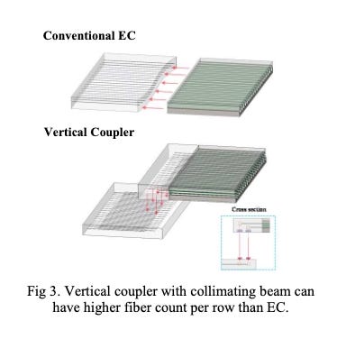
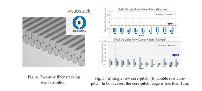
Source: TSMC
Power Handling and Energy Efficiency
High Power Tolerance:SiN waveguides support >25 dBm input power without degradation, unlike silicon waveguides which degrade due to nonlinear effects above 20 dBm.
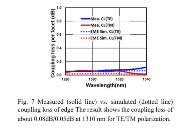
Low Coupling Loss:TE/TM coupling loss is measured at 0.08/0.05 dB. Alignment tolerance studies show robustness to 1.6 µm (Y/Z direction) and 36 µm (gap).

Source: TSMC
Waveguide Loss:Extracted propagation loss of 0.01 dB/cm and 90° bend loss of 0.001 dB.
Interlayer Transition:0.015 dB loss between layers.
Polarization Control:SiN-based PBSR achieves 23 dB ER with 0.3 dB insertion loss and 0.1 dB PDL.

Manufacturability and Field Maintenance
Maintainability:FAU system uses embedded silicon microlens arrays for collimated beam coupling, enabling field-replaceable optics with only 1.8 dB loss increase.
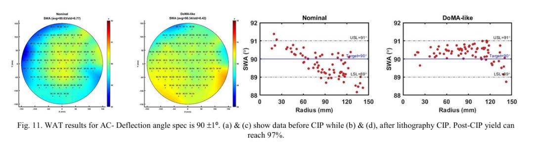
Process Compatibility:Fabricated using IC wafer-level processes, supporting in-line testing, automation, and optical WAT. 90° beam deflectors achieve 97% yield post-process optimization.
Source: TSMC
Broadcom vs. NVIDIA: A Comparison of CPO Switch Strategies

The key differences between Broadcom and NVIDIA’s CPO switches lie in their modulator architecture and wavelength strategy:
• Broadcom uses the more traditional MZM (Mach-Zehnder Modulator) with a multi-wavelength (WDM)approach, allowing for fewer fibers. Recently, Broadcom introduced a Bidi optical module for AI interconnects, supporting bi-directional transmission using only two wavelengths: 1270nm and 1310nm.

NVIDIA, on the other hand, adopts a single-wavelength MRM (Micro Ring Modulator) architecture. Though this increases fiber count, the modules are more compact and power-efficient. Its energy efficiency is 1.4 pJ/bit better than Broadcom’s, with room for further optimization.
Both companies use 1:4 laser splitting and have adopted pluggable laser modules for better maintainability.
NVIDIA’s CPO switch is first deployed in the Infiniband (IB) space, where it holds a monopoly, making commercial rollout smoother. In contrast, Broadcom’s Ethernet-based CPO efforts have faced more friction due to ecosystem complexity.
Meanwhile, LPO (Linear Pluggable Optics) modules—gaining popularity due to the absence of DSP—offer reduced power and cost, especially for short-reach scenarios. However, for longer-reach GPU interconnects, NVIDIA still prefers optics, while keeping copper for intra-rack links. As Jensen Huang put it at GTC:
“Use copper where you can, use optics if you must.”
Ultimately, CPO is not just about photonic chips—it encompasses advanced packaging, laser integration, optical coupling, thermal design, and full-stack engineering. Leveraging its world-class supply chain, NVIDIA has successfully mass-produced a CPO switch based on MRM, signaling the true beginning of the CPO era.
EPIC-BOE presents a scalable, manufacturable, and power-efficient platform for next-generation optical interconnects. Its use of vertical coupling, multi-row fiber alignment, and robust SiN waveguide integration addresses current limitations of EC and GC technologies. The innovative use of microlens-enhanced vertical coupling provides a practical and high-performance solution for scalable photonic systems.
Summary of Each Company’s CPO Strategy
•Intel: Has spun off its optical communication business, but retains control over SiPh (silicon photonics) process; provides Optical I/O directly for its own ASICs.
•Broadcom: Ambitious; aims to control everything related to CPO and SiPh.
•Marvell: Focuses on DSP as its core; maintains flexibility and a conservative approach to both SiPh and CPO solutions

Further Discussion Points
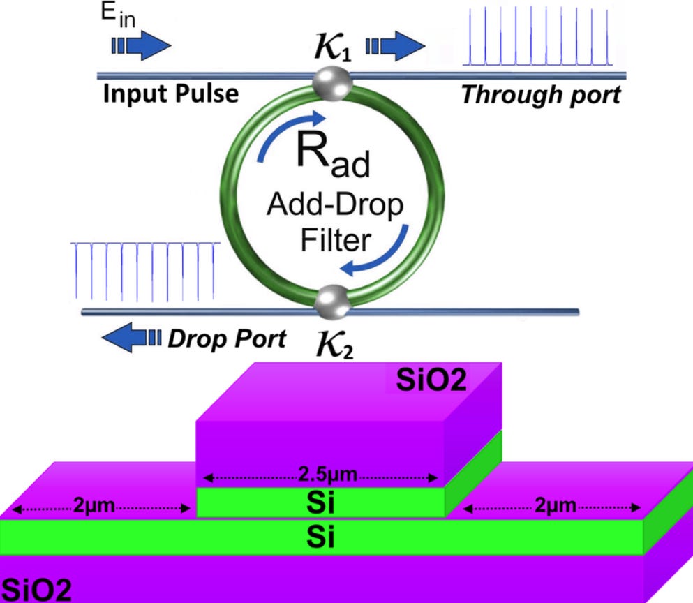
Although micro-ring modulator (MRM) designs offer advantages such as compact size, low power consumption, and high bandwidth density, they are also highly sensitive to process variation and temperature fluctuations. This makes resonance wavelength locking and tracking a challenging engineering task.
For years, the industry has questioned whether MRM-based modulators could be commercialized and scaled to volume production. NVIDIA has given a definitive answer—not only adopting the technology, but immediately pushing it to the next level by achieving 200 Gbps per channel, effectively eliminating doubts.
With this move, silicon photonics has officially entered the 200 Gbps-per-channel era.

Why Is NVIDIA Advancing Micro-Ring Modulators and CPO Technology?
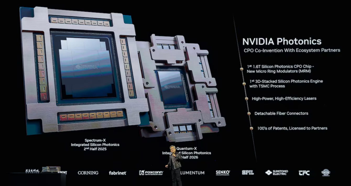
At OFC 2024, many presentations focused on Co-Packaged Optics (CPO), and the industry was still debating whether CPO had truly reached a commercially viable stage. One year later, the launch of a fully integrated CPO switch by NVIDIA provided a resounding “yes.”
Although neither Co-Packaged Optics (CPO) nor Micro-Ring Modulators (MRMs) are entirely new technologies, their combination delivers substantial improvements in energy efficiency, significantly reducing the power consumption and cost of network interconnects in AI clusters. This is the key motivation behind NVIDIA’s strong commitment to commercializing the technology.
After acquiring Mellanox in 2019, NVIDIA began mapping out its MRM development roadmap in 2020. The original architectural blueprint—partially revealed in early internal slides—has since been partially productized, with the remaining components still under active development.
To accelerate this progress, NVIDIA recruited top-tier silicon photonics engineers from Intel, including the renowned Intel Fellow Liao Ling, who has been working on MRM research since 2007. Her expertise, along with that of others, has played a vital role in transforming NVIDIA’s MRM-based CPO system into a reality.


PreviousNext
TopLatestDiscussions








See all