Can SMIC Overcome Its Bottleneck Solely Through DUV Immersion? SMIC vs TSMC?
Can SMIC Overcome Its Bottleneck Solely Through DUV Immersion? SMIC vs TSMC?
- Source: SemiVision
- Author: SEMIVISION
- Published: 2025-03-28T23:56:49+08:00
- URL: https://tspasemiconductor.substack.com/p/can-smic-overcome-its-bottleneck (1) Can SMIC Overcome Its Bottleneck Solely Through DUV Immersion? SMIC vs TSMC?


Can SMIC Overcome Its Bottleneck Solely Through DUV Immersion? SMIC vs TSMC?
Original Articles by SemiVision Research

Mar 28, 2025
∙ Paid
Before reading this article, you may refer to our previous articles on SEMICON China.
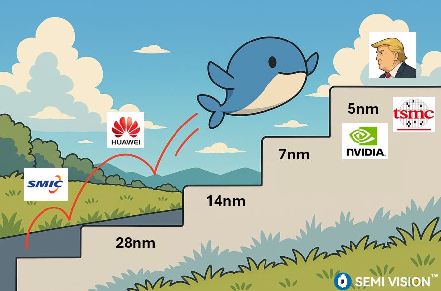
Semiconductor Manufacturing International Corporation (SMIC)has become a critical pillar in China’s push for self-sufficiency in high-end semiconductor manufacturing. As China’s largest and most advanced foundry, SMIC is at the forefront of developing AI chips that are vital for the country’s technological ambitions. According to insights from SemiVision Research, Huawei’s Ascend AI chips have demonstrated exceptional performance, positioning themselves as strong contenders against NVIDIA’s H20 AI accelerators. Ascend 910B, Huawei’s flagship AI chip, offers high training efficiency with computational performance exceeding 512 TFLOPs (FP16), optimized inference speed, and increased power efficiency due to its proprietary Da Vinci architecture. A key catalyst in this technological leap has been the emergence of DeepSeek, a leading Chinese AI model that is rapidly gaining prominence in the AI community. DeepSeek’s large language models (LLMs) and foundation models have been optimized to run on Ascend AI chips, creating a synergistic relationship that has accelerated the growth of China’s AI industry.
By aligning AI models with domestically produced hardware, China is reducing its dependence on foreign AI accelerators, ensuring greater control over its AI supply chain, and enabling faster deployment of AI applications across diverse industries, from smart cities to healthcare and autonomous driving. However, this progress is likely to escalate U.S. concerns over China’s technological autonomy, leading to stricter export controls.

The U.S. government is expected to expand the scope of export restrictions on critical semiconductor technologies, including EUV lithography, advanced GPUs, and semiconductor design tools, while also potentially limiting China’s access to AI training frameworks, cloud computing resources, and high-performance interconnect technologies essential for large-scale AI model development. The success of Ascend AI chips and DeepSeek models has positioned China as a formidable player in the global AI race, but this rapid progress is likely to provoke heightened scrutiny and control from the U.S. government, reflecting the intensifying competition in the global AI and semiconductor landscape where technological innovation and geopolitical strategy are increasingly intertwined.


NVIDIA is expected to phase out the production of its H-series AI chips at TSMC by the first half of 2025, shifting focus to the new B-series chips. According to internal sources, the transition will be seamless, with a one-to-one ratio of replacement between the H-series and B-series, ensuring no disruption in supply. The introduction of the B-series marks a significant shift in NVIDIA’s AI hardware strategy, as these new chips are expected to leverage Feynman’s architecture, which integrates cutting-edge innovations in semiconductor design and process technology. SemiVision Research has closely monitored this transition and observed that with each successive node migration to more advanced processes, NVIDIA continues to optimize for reduced leakage, lower power consumption, and increased transistor density. These improvements are critical for maintaining AI performance gains while addressing the growing challenges associated with scaling AI hardware.
At the same time, countries worldwide are strengthening their semiconductor ecosystems by injecting substantial financial resources to support domestic semiconductor industries and reduce reliance on foreign supply chains. Nations such as the United States, China, South Korea, Japan, and the European Union are ramping up investments in advanced semiconductor R&D, fabrication capacity, and AI infrastructure to secure technological leadership in the era of AI and high-performance computing. SemiVision Research has conducted in-depth analyses on these global initiatives, highlighting how government funding, coupled with private sector innovation, is driving the next phase of semiconductor growth and ensuring that countries remain competitive in the increasingly fragmented and geopolitically charged semiconductor landscape. This convergence of technological progress and strategic policy interventions underscores the critical importance of maintaining leadership in semiconductor manufacturing and AI hardware, where advancements in process technology, energy efficiency, and AI model optimization continue to shape the future of the industry.


TSMC, Intel and peers to slow Japan, Malaysia chip expansions- Nikkei
China’s cloud computing industry is also advancing aggressively, with Alibaba and ByteDance making significant investments to expand their cloud infrastructure and AI capabilities. These efforts align with China’s national strategy to achieve self-sufficiency in semiconductor manufacturing by fostering a complete “from design to manufacturing” ecosystem that encompasses not only domestic chip design but also the development of indigenous semiconductor equipment. SemiVision Research has previously conducted a comprehensive analysis comparing China’s semiconductor equipment manufacturers with international counterparts, revealing China’s determined push to establish a robust semiconductor ecosystem. This effort aims to build an end-to-end supply chain that integrates chip design, manufacturing, and packaging into a seamless “one-stop” ecosystem that reduces dependence on foreign technology. In this context, DeepSeek, one of China’s fastest-growing AI companies, has demonstrated a strong ambition to develop its own proprietary AI chip to optimize the performance of its AI models. To achieve this, DeepSeek has collaborated with multiple Chinese ASIC design companies, seeking to customize AI chips that align perfectly with its AI workload requirements. It is highly likely that SMIC (Semiconductor Manufacturing International Corporation), China’s leading foundry, will handle the manufacturing of these AI chips, ensuring that the fabrication process remains within China’s domestic semiconductor supply chain. For advanced packaging and assembly, DeepSeek is expected to partner with leading Chinese OSAT (Outsourced Semiconductor Assembly and Test) companies, leveraging their expertise in high-performance packaging technologies such as Chip-on-Wafer-on-Substrate (CoWoS) and Fan-Out Wafer-Level Packaging (FOWLP) to maximize the efficiency and scalability of its AI accelerators. DeepSeek’s strategy to develop a proprietary AI chip not only reflects the growing trend of vertical integration among AI companies but also highlights China’s determination to control the entire AI supply chain—from semiconductor design to manufacturing and packaging. As China’s semiconductor ecosystem continues to evolve, this drive for end-to-end control will accelerate the nation’s AI advancements and solidify its position as a formidable player in the global AI landscape.

DeepSeek, one of China’s leading artificial intelligence companies, has recently made headlines with reports of its plans to develop its own AI chips, drawing significant attention from the industry. According to reports, DeepSeek has launched a large-scale recruitment effort to hire professionals in chip design, aiming to accelerate its progress in chip self-development.
Developing its own chips holds strategic significance for DeepSeek on multiple fronts. Firstly, customized hardware can optimize the efficiency of model operations, reduce energy consumption, and enhance the company’s technological self-reliance. Secondly, with the rising costs and limited availability of high-end GPU chips, in-house chip development is expected to reduce long-term expenses and improve operational efficiency.
Currently, DeepSeek has collaborated with numerous domestic AI chip companies, with its models now compatible with more than 20 Chinese AI chip manufacturers, including Huawei Ascend. Additionally, DeepSeek’s R1 modeldemonstrated impressive performance during its training process, achieving significantly lower training costs compared to its American counterparts, showcasing the company’s innovative capabilities in resource-constrained environments.
However, the path to independently developing AI chips is far from easy. It involves navigating complex stages such as architecture design, instruction set optimization, tape-out testing, and mass production. Despite these challenges, DeepSeek’s initiative is seen as a crucial step for Chinese AI companies in pursuing technological self-sufficiency. It could potentially reshape the competitive landscape in sectors such as cloud computing and intelligent devices, redefining the rules of competition in these industries.

Due to the open-source release of DeepSeek’s models, the momentum of AI development in China has been significantly boosted. As a result, many CSPs (Cloud Service Providers) are now actively collaborating with DeepSeek, fostering mutual cooperation. Currently, as many as O companies are working closely with DeepSeek to develop ASIC chips and have partnered with SMIC (Semiconductor Manufacturing International Corporation) for manufacturing.
When it comes to AI chip packaging, CoWoS (Chip-on-Wafer-on-Substrate) remains the predominant choice. We have also observed that international CSPs are making concerted efforts to develop their own AI chips, primarily to reduce costs, as NVIDIA’s chips are becoming increasingly expensive.
However, Jensen Huang (CEO of NVIDIA) has pointed out that while many companies are developing their own ASIC chips, they must also consider the ecosystem. This is where NVIDIA’s moat, CUDA, comes into play, providing a significant competitive advantage. In contrast, most CSPs still lack a proprietary ecosystem, which is why NVIDIA remains the dominant force in AI data centers.

The most talked-about topic at SEMICON China 2025 was undoubtedly SiCarrier (新凱來), whose “Mountain Series” equipment has generated intense industry interest. SemiVision Research conducted an initial analysis of SiCarrier ’s next-generation equipment lineup, highlighting their potential to advance FinFET manufacturing processes. One area that deserves special attention is the Atomic Layer Deposition (ALD) process, which will play an increasingly critical role in advanced nodes. For 2nm and beyond, the frequency of ALD steps is expected to rise dramatically, making it a pivotal component in achieving high-yield, high-performance chip production. Notably, Huawei’s key suppliers are reportedly preparing to debut a 5nm chip developed using SiCarrier’s tools, with the product line aptly named “Ali Mountain” (阿里山), underscoring the company’s confidence in its advanced equipment.

According to a Reuters report, international media have shown heightened interest in SiCarrier’s growing role in China’s semiconductor ecosystem, particularly with its contributions to advancing domestic chipmaking technology.
At the same time, industry sources revealed another groundbreaking development atSEMICON China—Huawei has reportedly developed its first ArF Immersion Lithography toolfor14nm production lines, with mass production expected to begin between2026 and 2027.
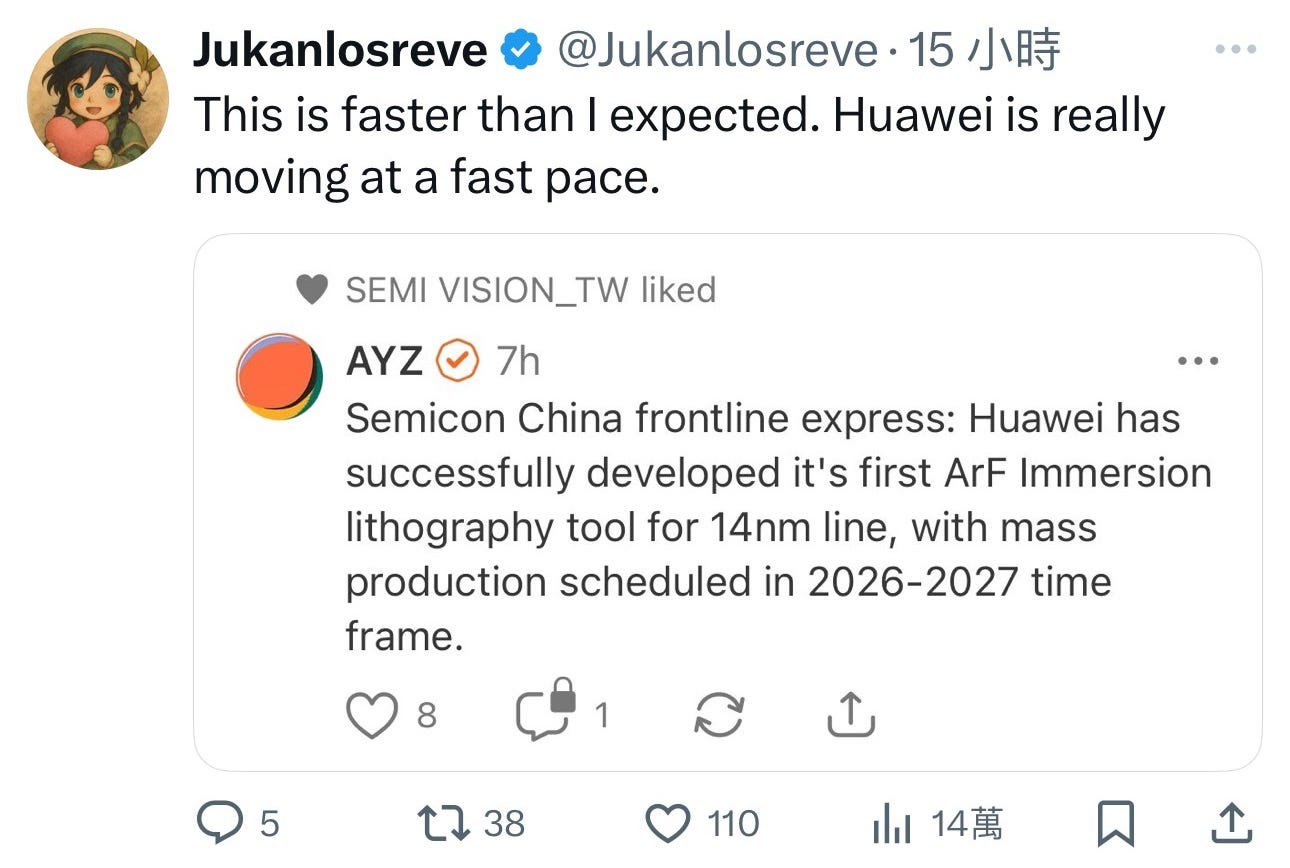

According toSemiVision Research, the current lithography equipment supplier in China isSMEE (Shanghai Micro Electronics Equipment Co., Ltd.) and SiCarrier (新凱來), but in reality, its focus is primarily onDUV (Deep Ultraviolet) lithography technology.


This milestone marks a major step toward China’s semiconductor self-sufficiency, as immersion lithography is critical for producing advanced nodes below28nm. Huawei’s achievement signals a potential shift in the global lithography landscape, as China accelerates efforts to develop indigenous lithography solutions that could reduce reliance on foreign suppliers. The combination of SiCarrier’s advanced deposition equipment and Huawei’s breakthrough in immersion lithography suggests that China is building a robust, vertically integrated semiconductor supply chain, capable of supporting cutting-edge chip manufacturing and positioning itself as a formidable player in the global semiconductor market.

SiCarrier says its tools can help China make advanced chips (Reuters)

SemiVision Research believes that while China has made some progress in DUV (Deep Ultraviolet) lithography and EUV (Extreme Ultraviolet) lithography, its breakthroughs have primarily been in the light source segment. However, the complexity of lithography equipment goes far beyond just the light source, requiring advancements across multiple domains. For instance, ASML’s EUV lithography machine is one of the most sophisticated and precise pieces of equipment in modern semiconductor manufacturing. Each EUV machine consists of over 100,000 individual components, including 3,000 wires, 40,000 bolts, and 2 kilometers of tubing. Once fully assembled, the machine is about the size of a small bus and weighs between 150 to 180 tons. Due to its massive size and intricate design, these machines are typically disassembled into around 250 separate crates for transportation, including 13 large shipping containers. These details highlight the extreme complexity and precision involved in designing and manufacturing EUV lithography equipment.
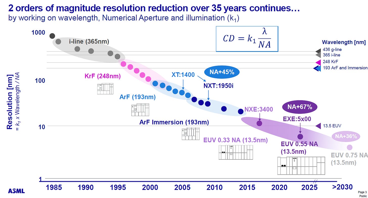
In addition to the challenges related to the machine’s physical structure, the optical system of the EUV lithography machine presents another formidable hurdle. ASML’s EUV machines rely on an advanced multilayer reflective mirror system developed by Zeiss, with precision at the nanometer level. Each of these mirrors must maintain surface errors below 0.1 nm to ensure accurate reflection of the EUV light, a level of optical precision that remains beyond China’s current technological capabilities. Moreover, the light source used in EUV lithography is generated by tin (Sn) plasma, producing 13.5nm wavelength extreme ultraviolet light, which requires extremely high power inputs to maintain a stable exposure process. Additionally, the system operates in a high vacuum environment, making the development of a domestic EUV machine in China exceptionally difficult. Even if breakthroughs are achieved in light source technology, China would still face a series of challenges related to optical systems, mirror fabrication, precise motion control, and maintaining ultra-high vacuum conditions. Therefore, developing an indigenous EUV lithography machine will require prolonged technological accumulation and industrial collaboration.
On the other hand, photoresist is another critical component that poses challenges for domestic lithography efforts. EUV photoresists must offer higher resolution and better etch resistance, while perfectly matching the wavelength of EUV exposure. Currently, the high-end photoresist market is dominated by companies such as JSR, TOK, Sumitomo Chemical, Shin Etsu, Fujifilm in Japan, and Dupont in the United States. Although China has made progress in the field of photoresists, it will take a considerable amount of time and close collaboration with suppliers to optimize these materials to meet the demands of EUV lithography.


As a result, SemiVision Research believes that while China has made some advancements in DUV lithography, developing an EUV lithography machine remains a formidable challenge that cannot be overcome in the short term. DUV lithography is a more feasible option for China, but even in this domain, success requires more than just a single technological breakthrough. It necessitates a comprehensive ecosystem and technological integration across multiple domains, including light sources, optical systems, photoresists, precision motion control, and vacuum environment maintenance, to achieve true competitiveness in lithography equipment. Therefore, while China can continue to make steady progress in DUV technology, achieving a breakthrough in EUV lithography will require much more time, technological accumulation, and continuous improvements in supply chain and ecosystem integration to narrow the gap with ASML.
For Paid Members, SemiVision Research will discuss following topics
Maximizing DUV Potential: China’s Strategic Path to Achieve Advanced Semiconductor Nodes
Introduction to DUV Immersion Lithography (ArFi) and Double Patterning
Leading DUV ArFi Lithography Machines
Current Market Status and Trends
China’s Semiconductor Progress: Latest Developments in DUV and EUV Lithography Equipment
Breakthrough in Solid-State Laser Technology: A Potential Game-Changer for DUV Lithography
Strategic Implications for the Semiconductor Industry in Solid State DUV
Insights from SemiVision Research: Analyzing Semiconductor Supply Chain Trends from SEMICON China 2025
Semiconductor Export Controls: Tensions Between China and Japan
Material Innovation in CoWoS and HBM Material / Equipments
2025 Semiconductor Materials Technology Breakthroughs: Building a Comprehensive Materials Ecosystem Matrix
Semiconductor Material Innovation: The Next Battleground
Latest Status Update on SMIC: Advancements and Customer
Short comment on China lithography development by SemiVision Research
Maximizing DUV Potential: China’s Strategic Path to Achieve Advanced Semiconductor Nodes
SemiVision Research has conducted an in-depth analysis of China’s current progress in Deep Ultraviolet (DUV) lithography and explored the potential for leveraging DUV to produce advanced semiconductor nodes. Given China’s current limitations in Extreme Ultraviolet (EUV) lithography technology, ArF Immersion (ArFi) lithography remains the most viable path for producing chips at 28nm and below. To extend DUV capabilities to more advanced nodes, Double Patterning Technology (DPT) plays a pivotal role. Double patterning, which involves multiple exposure and etching steps to increase feature density, is essential to push DUV to the limits of its resolution. Self-Aligned Double Patterning (SADP) and Litho-Etch-Litho-Etch (LELE) methods are commonly used to achieve critical dimensions below 28nm with DUV systems. While this approach requires significantly more process complexity and longer cycle times, it remains China’s best option for producing sub-14nm nodes domestically.
As Huawei and SMIC continue to refine their DUV-based manufacturing processes, the application of DPT combined with advanced process control and improved overlay accuracy could allow China to gradually narrow the technology gap with international competitors. Although DUV-based double patterning is not as efficient as EUV for advanced nodes, China’s strategic focus on enhancing its DUV capabilities underscores its determination to achieve greater technological autonomy in the semiconductor industry.
Introduction to DUV Immersion Lithography (ArFi) and Double Patterning
Deep Ultraviolet (DUV) Immersion Lithography using argon fluoride (ArF) excimer lasers has become a critical technology in advanced semiconductor manufacturing. Operating at a wavelength of 193 nm, DUV lithography uses an immersion technique that places a thin layer of ultra-pure water between the photomask and the wafer. This approach enhances the numerical aperture (NA) beyond 1.0, typically up to 1.35 NA, effectively reducing the wavelength to around 134 nm and significantly improving resolution. This innovation enables the production of smaller feature sizes and has extended the applicability of DUV lithography to nodes as small as 14 nm and beyond.
However, as the limits of DUV lithography were approached, the industry adopted double patterning (DP) techniques to overcome these challenges. Double patterning allows for finer geometries by splitting a single pattern into multiple exposure and etching cycles. Among the most common DP techniques are Litho-Etch-Litho-Etch (LELE), Spacer-Assisted Double Patterning (SADP), and Litho-Freeze-Litho-Etch (LFLE). LELE splits the original pattern into two exposures with intermediate etching, effectively halving the pitch size. SADP involves adding spacers around pre-patterned structures, while LFLE freezes one pattern and then exposes a second pattern to achieve higher density.
Using these techniques, the minimum feature size achievable with DUV ArFi lithography has been dramatically reduced. While a single exposure with ArFi can achieve a minimum line width of around 38-40 nm, double patterning techniques can shrink the feature size to 20-28 nm, which corresponds to the 10-14 nm process nodes. In some cases, quadruple patterning (QP) is employed for even finer features, although this introduces higher complexity and increased cost.
Leading DUV ArFi Lithography Machines
In the DUV lithography market, three major players dominate the industry:ASML, Nikon, and Canon.

ASMLleads the market with its advancedTWINSCAN NXTseries, including theNXT:2000i, NXT:2050i, and NXT:2100isystems, which feature an NA of1.35and are capable of achieving resolutions of38-40 nmwith single patterning and20-28 nmthrough double patterning. These systems are widely used for producing chips at 14 nm, 10 nm, and even 7 nm nodes through multiple patterning techniques. TheNXT:1980Dimodel is another workhorse used extensively in 28 nm, 22 nm, and 14 nm production.
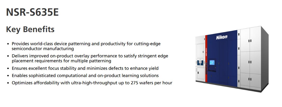
Nikonis another key player, particularly strong in the Japanese semiconductor ecosystem. ItsNSR-S635EandNSR-S622Esystems are capable of achieving comparable resolutions to ASML’s models, supporting advanced nodes down to 14 nm and 10 nm through double patterning. These machines have been adopted by major foundries and DRAM manufacturers.
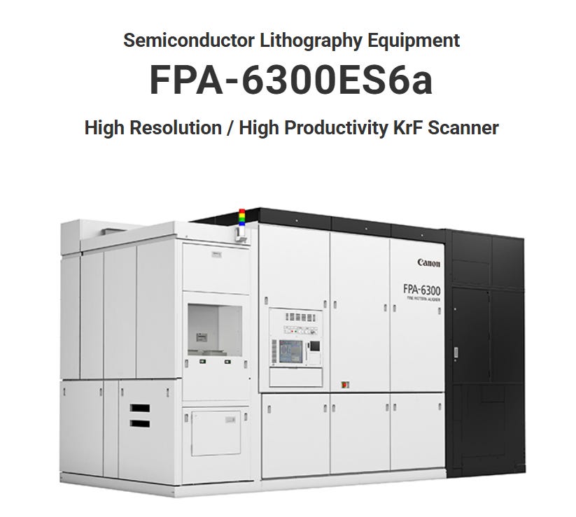
Canon, while more focused on mature process nodes and niche applications, also contributes to the DUV lithography landscape. ItsFPA-6300ES6asystem, with an NA of 1.35, supports nodes down to 28 nm, while the olderFPA-6000 serieshas been used for 45 nm and 32 nm nodes.
Current Market Status and Trends
ASML dominates the high-end DUV and EUV lithography market, with an estimated85% market sharein the DUV immersion segment. Nikon maintains a strong presence in Japan, serving domestic foundries and memory manufacturers. Canon, although less active in advanced lithography, continues to play a role in providing solutions for mature nodes.
With the continued advancement of semiconductor manufacturing,DUV ArFi lithography combined with double patterningremains a vital technology for producing nodes such as 14 nm, 10 nm, and 7 nm. While Extreme Ultraviolet (EUV) lithography is increasingly used for the most advanced nodes, DUV immersion remains a cost-effective and reliable solution for high-volume production.

China’s Semiconductor Progress: Latest Developments in DUV and EUV Lithography Equipment
China has made significant progress in the field of Deep Ultraviolet (DUV) lithography technology, with several key research institutions driving these advancements. The Chinese Academy of Sciences (CAS) recently developed a solid-state DUV laser source capable of emitting coherent light at a wavelength of 193nm, which holds great potential for application in advanced semiconductor lithography processes. This innovation offers an alternative approach to DUV lithography and could provide a pathway for China to enhance its chip manufacturing capabilities. Meanwhile, Shanghai Micro Electronics Equipment (SMEE), China’s leading lithography equipment manufacturer, has successfully completed the initial development of its SSA800-10W immersion lithography system, which is capable of producing 28nm-class chips and is reportedly being used by SMIC and other domestic manufacturers. In addition, SiCarrier, a prominent Chinese semiconductor equipment company, has developed a wide range of etching, deposition, and metrology tools that have been deployed at major Chinese fabs, including those of Huawei and SMIC, despite the impact of U.S. export controls. Furthermore, China’s Ministry of Industry and Information Technology (MIIT)recently announced that the country’s first domestically developed DUV lithography system has successfully been commercialized, with the ability to produce chips at 8nm and below, and is currently being deployed in production lines.
Breakthrough in Solid-State Laser Technology: A Potential Game-Changer for DUV Lithography
In March 2025, a groundbreaking development in the global semiconductor industry has emerged from a research team at the Chinese Academy of Sciences (CAS). The team successfully developed a deep ultraviolet (DUV) light source system based on solid-state laser technology that can generate coherent light at a wavelength of 193 nm, theoretically supporting 3nm chip manufacturing. This achievement marks a significant step forward in advancing lithography light source technology and could potentially reshape the competitive landscape of the global semiconductor supply chain.
Understanding the Core: DUV Lithography and Its Limitations
Lithography, the backbone of semiconductor manufacturing, functions similarly to a high-precision “projector,” transferring circuit patterns onto silicon wafers at the nanometer scale. The wavelength of the light source directly determines the precision of the chip manufacturing process. Currently, leading global lithography companies such as ASML (Netherlands), Nikon, and Canon (Japan) rely on argon fluoride (ArF) excimer laser technology to generate DUV light at 193 nm. However, this technology depends on rare gases, involves complex systems, and consumes large amounts of energy. Moreover, the key patents in this domain have been long monopolized by overseas companies, presenting a formidable challenge for emerging semiconductor ecosystems.
A Disruptive Approach: Solid-State Laser Innovation
The CAS team’s success lies in bypassing traditional excimer laser technology and introducing an innovative solid-state laser solution. Their system uses a Yb:YAG crystal amplifier to generate a 1030 nm laser, which is then split into two optical paths for wavelength conversion:
One path generates a 258 nm laser through a fourth harmonic generation (FHG) process.
The other path produces a 1553 nm laser through optical parametric amplification (OPA).
These two beams are subsequently combined in a lithium triborate (LBO) crystal to generate a 193 nm light source. This approach circumvents the patent barriers held by companies like ASML and significantly reduces the size, energy consumption, and reliance on rare gases in lithography light sources.
Key Advantages of This Breakthrough
Autonomous and Innovative Technological Pathway
Traditional DUV lithography using excimer lasers involves a highly complex gas excitation system and precision optics, with the supply chain heavily concentrated among US, European, and Japanese companies. The solid-state approach developed by CAS introduces a disruptive alternative that allows for independent intellectual property rights in the core module of lithography systems.
For instance, the experimental system has demonstrated the ability to generate vortex beams with orbital angular momentum, which holds unique potential in wafer processing and defect inspection, paving the way for further technological advancements.
Synergistic Impact on the Semiconductor Supply Chain
The adoption of solid-state laser technology introduces new demands on upstream materials. Critical materials such as Yb:YAG crystals and LBO crystals play a decisive role in commercializing this technology.
Balancing Performance and Cost: A Paradigm Shift
Conventional DUV lithography systems require excimer lasers with output power exceeding 100-120W and pulse frequencies of 8-9 kHz. In contrast, the current CAS prototype system operates at 70 mW power and 6 kHz frequency, a significant gap from commercial standards. However, the scalability of solid-state laser technology offers promising potential for improvement.
With optimization in crystal thermal management and higher laser amplifier efficiency, this technology could gradually approach commercial performance benchmarks. More importantly, eliminating the need for complex gas circulation systems may reduce maintenance costs by over 30%, a critical advantage in the highly cost-sensitive chip manufacturing market.
Strategic Implications for the Semiconductor Industry in Solid State DUV
If this solid-state DUV light source can be successfully commercialized in the next 3-5 years, it would provide an alternative pathway for producing chips ranging from 28nm to 7nm nodes, covering more than 80% of global semiconductor demand in sectors such as automotive electronics, industrial control, and IoT devices.
Furthermore, this innovation opens up new possibilities for the development of extreme ultraviolet (EUV) light sources. By potentially replacing current tin-droplet plasma-based EUV light sources with solid-state laser technology, the next generation of lithography systems could achieve higher stability, lower operational costs, and greater energy efficiency, positioning the technology as a differentiated advantage in the future of semiconductor manufacturing.
Challenges to Commercialization: Hurdles Yet to Overcome
Despite the immense potential of this breakthrough, achieving commercial-scale application still requires overcoming several significant hurdles:
Power Scaling and Physical Limitations
The energy conversion efficiency of solid-state lasers is constrained by the properties of nonlinear optical crystals, requiring advancements in damage thresholds of optical components. Currently, the average output power of the experimental system is only 0.07 watts, while ASML’s commercial DUV systems achieve up to 120 watts, highlighting a disparity of over 1700x.
System Integration Complexity
Integrating the light source with lens systems, wafer stages, and other critical modules remains a complex challenge.
ASML’s DUV lithography systems consist of over 100,000 components sourced from more than 5,000 global suppliers. Developing comparable precision in optics, motion control, and alignment systems will take time and substantial industry collaboration.
Process Adaptation for High-Precision Manufacturing
Manufacturing 3nm chips requires advanced multi-patterning techniques that impose stringent demands on the stability and uniformity of the light source. While the current prototype’s spectral purity is comparable to commercial systems, long-term operational challenges such as thermal drift and vibration interference need to be rigorously tested in mass production environments.
A Potential Disruption in Lithography Technology
This breakthrough in solid-state DUV laser technology presents an unprecedented opportunity to diversify the global semiconductor supply chain and pave the way for next-generation lithography solutions. While commercialization remains a formidable challenge, continuous advancements in power scaling, system integration, and process adaptation could position this innovation as a viable alternative to existing DUV and EUV solutions.
If successful, this technological evolution will not only enhance the resilience of the semiconductor ecosystem but also introduce a new dimension of competition in the global lithography market.
Insights from SemiVision Research: Analyzing Semiconductor Supply Chain Trends from SEMICON China 2025
SemiVision Research has closely analyzed the trends emerging from SEMICON China 2025, which attracted a large number of semiconductor material suppliers, highlighting the critical role that materials and equipment play in driving advanced semiconductor manufacturing processes. Within the supply chains of CoWoS (Chip-on-Wafer-on-Substrate)and HBM (High Bandwidth Memory) technologies, suppliers can be broadly categorized into two groups: equipment suppliers that provide cutting-edge lithography, deposition, etching, and metrology tools, and material suppliers that supply essential semiconductor materials such as photoresists, CMP slurries, wafer substrates, and bonding materials. Upon deeper examination, it becomes evident that Japan continues to dominate the semiconductor materials supply chain, particularly in advanced lithography technologies, where Japanese companies maintain an irreplaceable advantage. This dominance has created a complex dynamic of competition and strategic maneuvering between China and Japan in the semiconductor sector, reflecting a broader geopolitical and technological rivalry that extends beyond the supply chain. Japan’s stronghold in photoresists, ultra-pure chemicals, and specialty materials used in advanced lithography, including EUV and ArF immersion processes, poses a significant challenge for China’s efforts to build a fully self-sufficient semiconductor ecosystem. As China aggressively pursues supply chain independence through domestic innovation and increased investment in semiconductor materials, Japan’s established dominance in this space adds another layer of complexity to China’s semiconductor ambitions. These underlying tensions and competitive dynamics underscore the ongoing evolution of the global semiconductor landscape, where supply chain resilience and technological sovereignty are becoming increasingly critical for national security and economic competitiveness.
Semiconductor Export Controls: Tensions Between China and Japan
In recent years, semiconductor export control measures betweenChina and Japanhave drawn significant global attention.
Japan’s Export Restrictions on Semiconductor Equipment
In July 2023, the Japanese government imposed export controls on 23 types of advanced semiconductor manufacturing equipment. While China was not explicitly mentioned, the move was widely interpreted as targeting China.
China expressed serious concerns about these restrictions, stating that they could jeopardize the security and stability of supply chains and harm the interests of companies in both countries.
China’s Response: Export Controls on Critical Materials
In August 2023, China retaliated by imposing export controls on gallium and germanium, two critical materials used in semiconductor manufacturing. Exporters were required to obtain licenses to ship these materials.
Since Japan is a major importer of these materials, the restrictions had a direct impact on Japan’s semiconductor industry. By February 2025, Japanese officials and industry leaders expressed concerns that China’s export restrictions on semiconductor materials threatened the stability of the global electronics supply chain.
Japan Expands Export Controls in 2025
In January 2025, the Japanese government announced plans to impose additional export controls on over a dozen semiconductor-related items and added several Chinese companies to its End-User List.
In response, China’s Ministry of Commerce expressed concern, stating that the move could disrupt normal commercial exchanges between the two countries.
Impacts on Global Semiconductor Supply Chains
These reciprocal export controls between China and Japan highlight the complex and evolving trade relationship in the semiconductor sector.
The measures have not only disrupted normal business interactions between companies from both countries but have also had far-reaching effects on the global semiconductor supply chain, adding uncertainty to the industry and intensifying geopolitical tensions.
Material Innovation in CoWoS and HBM Material / Equipments
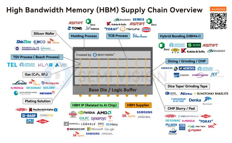
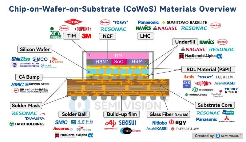
2025 Semiconductor Materials Technology Breakthroughs: Building a Comprehensive Materials Ecosystem Matrix
With the continuous evolution of global semiconductor technology,process materials, photoresists, CMP materials, electronic specialty gases, precursors, and packaging materialsare driving the industry’s advancement. Below is a detailed analysis of the latest technological developments and application scenarios in each domain.
The Critical Role of Japan in Semiconductor Materials: A Deep Dive into Key Areas
Japan maintains a commanding influence in the global semiconductor materials supply chain, covering several essential areas, with its dominance in Extreme Ultraviolet (EUV) photoresists being particularly critical for the advancement of leading-edge process nodes. EUV lithography is the backbone of producing 5nm, 3nm, and even more advanced nodes, and the precision and quality of photoresists play a foundational role in ensuring the success of these processes. Japan’s global leadership in EUV photoresist technology is exemplified by companies such as JSR Corporation, a pioneer whose high-performance EUV photoresists enable finer patterning and higher yields; Tokyo Ohka Kogyo (TOK), a leader in photolithography materials that develops materials aligned with the stringent requirements of EUV processes; and Shin-Etsu Chemical, known for its innovative photoresist formulations that enhance the reliability and consistency of EUV lithography.
Japan’s Irreplaceable Position in EUV Photoresist Supply
The dominance of Japanese suppliers in EUV photoresists is due to several factors. First, the high technical barriers and intellectual property protection surrounding EUV photoresist development make it extremely difficult for other countries to catch up. These photoresists require ultra-high purity, chemical stability, and precise formulations to withstand the intense energy generated by EUV photons. Japan’s decades of expertise and deep IP portfolio have made them indispensable partners for TSMC, Samsung, Intel, and other leading foundries. Second, the limited availability of alternative sources makes Japan’s position in the supply chain a strategic risk for other nations. Although China is aggressively pursuing semiconductor self-sufficiency, the complexity and high investment required to develop high-performance EUV photoresists make it nearly impossible to replace Japan’s leadership in the short term. Third, Japan’s control over these critical materials has created a significant geopolitical and supply chain vulnerability, especially as the global semiconductor competition intensifies. As China accelerates efforts to reduce its dependence on foreign suppliers, this dependence on Japan for critical materials has fueled growing competition and technological friction between the two nations.
China’s Response: Strengthening Domestic Semiconductor Supply Chains
In response to Japan’s dominance in critical materials, China is accelerating efforts to develop a domestic semiconductor ecosystem capable of reducing reliance on foreign technologies. China is investing heavily in photoresist R&D, with the goal of achieving breakthroughs in EUV-compatible materials. However, challenges such as maintaining high purity, ensuring chemical stability, and achieving process compatibility with leading-edge nodes continue to hinder China’s progress. At the same time, Chinese companies are actively pursuing strategic partnerships and acquisitions with global material suppliers to gain access to key technologies and accelerate the localization of critical materials.
Japan’s Continued Influence Across Semiconductor Materials
Beyond EUV photoresists, Japan maintains a dominant position in other critical semiconductor materials, including CMP (Chemical Mechanical Planarization) slurries and polishing pads, which are essential for achieving planarization in nodes below 7nm. Japan is also a leader in photoresist developers and chemical solutions tailored for ArFi (193nm immersion lithography) and EUV processes, influencing both resolution and yield. Additionally, Japan controls the supply of specialty gases and wafer substrates that ensure process stability and high yield in advanced semiconductor manufacturing.
Japan’s Strategic Position in the Global Semiconductor Ecosystem
Japan’s leadership in EUV photoresists and other critical semiconductor materials ensures its strategic leverage in driving the development of advanced process technologies. As the market demand for 3nm, 2nm, and beyond nodes continues to grow, Japan’s ability to supply these indispensable materials will maintain its dominance in the global semiconductor supply chain. While China continues its efforts to localize semiconductor materials, the long-term challenges of catching up with Japan’s technological expertise, particularly in EUV photoresists, highlight the persistent gap between the two nations. This ongoing competition between China and Japan in semiconductor materials will not only shape the future of global supply chains but also determine the trajectory of the semiconductor industry’s evolution.
Semiconductor Material Innovation: The Next Battleground
Insights from SEMICON China 2025 underscore that material innovation and supply chain resilience will be the defining factors in determining future semiconductor competitiveness. The ability of nations to secure and control critical materials will not only reshape the global semiconductor landscape but also dictate the pace of technological advancement and industrial leadership in the years to come.
Process Materials: Building “Super Factories” with Atomic-Level Precision
Photoresists and Supporting Materials: Full-Wavelength “Group Operations”
北京科华 demonstrated its 28nm KrF photoresist solution, achieving sidewall verticality of 90°±0.5°and a yield rate of 99.5%, validated by 长江存储(Yangtze Memory Technologies Co., Ltd.) for mass production.
南大光电 showcased its ArF photoresist with a yield rate of 99.2% at 中芯国际(SMIC)’s 14nm production line, along with EUV precursor materials, forming a complete ecosystem with 上海微电子设备(SMEE).
徐州博康 presented its i-line photoresist with a resolution breakthrough of 1.5μm and metal ion content of less than 0.01ppb, entering the TSV packaging market and signing a joint development agreement with 长电科技(JCET Group).
CMP Materials: Micron-Level “Grinding Revolution”
“International + Domestic” Dual Competition
3M’s Trizact™ polishing pad paired with fluorine-free conditioners achieved surface roughness of less than 0.5nm in 12-inch copper processes, reducing metal contamination by 65%.
安集科技 introduced its third-generation oxide CMP slurry, validated in 长江存储(YMTC)’s 3D NAND processes, with dish-shaped defect control at ±2nm and a lifespan increase of 40%.
鼎龙股份’s polishing fluid additives achieved 99.999% purity, forming a closed-loop material ecosystem with 江丰电子’s ultra-pure copper targets, reducing resistance by 15%.
Wet Electronic Chemicals and Specialty Gases: The “Lifeblood” of Ultra-Pure Ecosystems
江化微developed 9N-grade electronic sulfuric acid with metal ion content less than 0.1ppb, achieving 95% utilization efficiency through its regeneration system and reducing carbon emissions by 40%.
湖北兴福电子 produces IC-grade phosphoric acid (99.999%) and hydrogen peroxide with metal ion content less than 0.05ppb, certified by SEMI and applicable to 中芯国际(SMIC)’s 28nm process.
华特气体’s arsine/phosphine with impurities below 0.1ppb passed ASML certification, supporting high-end lithography equipment.
金宏气体’s ultra-pure ammonia (9N+) supports 中微半导体(AMEC)’s 5nm etching equipment, demonstrated in a collaborative process with 北方华创(NAURA)’s ion implanters.
Thin Films and Precursors: Advancing Atomic Layer Deposition (ALD) Technology
源展新材料 offers liquid boron/phosphorus precursors with impurity levels below 0.1ppm, supporting 北方华创’s ion implanters, achieving 14nm uniformity ±3%.
南大光电’s HfO₂ precursor (purity 99.9999%) reduced gate defect density to less than 10³ cm⁻² in 长鑫存储(CXMT)’s 5nm process.
微釜半导体 introduced silicon nitride thin film deposition technology (uniformity ±1.5%), applicable to power devices, memory, and advanced logic chips, signing a 12-inch production line verification agreementwith 长江存储(YMTC).
Packaging Materials: Driving the “3D Stack Revolution”
Advanced Packaging Adhesives: Enhancing 3D Stacking with “Liquid Armor”
长电科技’s 0.05mm ultra-fine pitch underfill (Tg>150℃) achieved 99.5% yield in 7nm 3D stacking processes, showcasing automotive-grade wide temperature range testing (-40℃~150℃).
汉高’s LCM 1000AG-1 adhesive filled at 50mm/s with a void rate below 0.5%, improving FO-WLP efficiency by 30% for AI chips.
日东电工’s temporary bonding adhesive achieved peel force below 5N/cm with residue less than 0.1μm, adapted to 12-inch TSV stacking (warpage<10μm), forming a front-end to back-end synergy with 3M’s CMP pads.
Thermal Management and Sealing: “Fortified Defense” for Extreme Environments
贺利氏’s sintered silver (Ag≥99.9%) achieved thermal conductivity above 200W/m·K, reducing thermal resistance by 40% for HBM3 modules, attracting interest from AMD and NVIDIA.
世索科 introduced fluorine-free perfluoroelastomers (Tecnoflon® FFKM NFS), achieving leakage rates below 1×10⁻⁹ Pa·m³/s in 300℃/-50℃ cyclic tests, debuting its PFAS-free technology at the ESG Forum.
资腾科技 developed thermal interface materials (TIMs) with thermal resistance below 0.1℃·cm²/W, supporting AI chip liquid cooling solutions and securing contracts with three computing companies.
Third-Generation Semiconductor Materials: Driving the “Large-Size SiC Revolution”
天岳先进 showcased a complete series of 6/8/12-inch SiC substrates, achieving micro-pipe density below 1 cm⁻² in 12-inch high-purity substrates, supporting 华为(Huawei)’s 800V EV platform.
天科合达’s 8-inch optical-grade substrates (transmittance>95%) and 12-inch heat sink substratestarget the AR glasses market, with P-type 6-inch substrates advancing automotive-grade validation.
浙江晶瑞debuted its 12-inch polycrystalline SiC substrates and 8-inch optical-grade ingots, partnering with 龙旗科技(Longcheer Technology) to plan mass production of smart glasses by 2027.
Auxiliary Materials: “Invisible Heroes” Behind Clean Processes
纯水一号’s six-stage ultra-pure water system (resistivity 18.2MΩ·cm, TOC<5ppb) covers 12-inch wafer fabs, signing a water treatment system agreement with 中芯国际(SMIC).
清软微视’s Alpha Series defect inspection equipment (precision 0.1μm) integrates with AI re-inspection software, boosting customer yield by 2%.
Material Ecosystem: Driving a “Chain Reaction” Between Equipment and Materials
•Equipment-Material Synergy:
•北方华创离子注入机 + 源展前驱体(14nm uniformity ±3%)
•中微刻蚀机 + 有研新材钽靶(grain size<50nm, lifespan 2x longer)
•新凯来 ALD 设备 + 南大光电前驱体(5nm defect density<10³ cm⁻²)
•ESG-Compliant Materials:
•江化微再生系统(95% reagent utilization)
•世索科无氟橡胶(eliminating PFAS)
•3M 无氟修整器(fluorine-free trimmers)
•2025 Materials Carbon Footprint White Paperindicates a47% reduction in carbon emissions per process unit.
Materials Technology Breakthroughs Driving Semiconductor Process Competitiveness
Latest Status Update on SMIC: Advancements and Customer
As the global semiconductor supply chain becomes clearer, it is evident that China is accelerating its efforts toward localization. SemiVision Research has compiled a comprehensive series of reports comparing Chinese suppliers with global suppliers, providing up-to-date insights on recent developments. SMIC (Semiconductor Manufacturing International Corporation) is positioned as the driving force behind China’s semiconductor industry, while Huawei plays the role of an innovation leader, and Chinese cloud service providers focus on enabling downstream applications. SemiVision Research believes that SMIC will continue to enhance its 3nm process capabilities in the future. Currently, 3nm manufacturing is primarily based on FinFET architecture, and SMIC is focusing on reducing the number of mask layers in N7/N5/N3 processes. By improving lithography techniques and lowering defect ratios, SMIC aims to achieve higher yield rates and strengthen its competitiveness in advanced nodes. Additionally, SemiVision’s analysis indicates that SMIC’s key customers include Qualcomm, Rockchip, Canaan, Huawei, Baidu, Alibaba, Horizon Robotics, and DeepSeek, highlighting a diverse ecosystem of AI, cloud, and semiconductor partners driving China’s technological growth.


Qualcomm:Founded in 1985 and headquartered in San Diego, California, Qualcomm is a global leader in wireless technology innovation and a supplier of semiconductors and telecommunications equipment. The company is renowned for its Snapdragon series of mobile processors, widely used in smartphones, tablets, and other mobile devices. Additionally, Qualcomm has significant influence in 5G technology, the Internet of Things (IoT), and automotive electronics.
瑞芯微电子股份有限公司(Rockchip):Established in 2001 and headquartered in Fuzhou, China, Rockchip is a professional integrated circuit design company. The company focuses on the design of mobile internet and digital multimedia chips, providing system-on-chip (SoC) solutions for personal mobile information terminals. Rockchip’s products are widely used in tablets, personal computers, streaming media TV boxes, AI audio and visual devices, and IoT hardware.
嘉楠科技(Canaan):Founded in 2013 and headquartered in Hangzhou, China, Canaan is a leading ASIC chip design company specializing in high-performance computing chips and equipment development. The company’s business encompasses blockchain computing devices and AI chip product development. Canaan is recognized as the world’s first blockchain enterprise to be listed on the NASDAQ and the first Chinese company with proprietary AI chip technology to be listed in the U.S.
华为技术有限公司(Huawei):Established in 1987 and headquartered in Shenzhen, China, Huawei is a global leader in ICT (Information and Communications Technology) infrastructure and smart devices. The company’s business spans telecommunications networks, IT, smart devices, and cloud services. In recent years, Huawei has made significant advancements in artificial intelligence and semiconductors, launching the Ascend series of AI processors aimed at propelling the AI industry forward.
百度(Baidu):Founded in 2000 and headquartered in Beijing, China, Baidu is the world’s largest Chinese-language search engine company. Beyond its search business, Baidu has invested heavily in artificial intelligence, autonomous driving, and cloud computing. Its AI products, such as the Ernie Bot, have garnered widespread attention in the market.
阿里巴巴集团(Alibaba):Established in 1999 and headquartered in Hangzhou, China, Alibaba is a global leader in e-commerce and cloud computing. The company’s business covers online retail, payment services, logistics, cloud computing, and digital entertainment. In recent years, Alibaba has also ventured into artificial intelligence and chip design, developing proprietary AI chips to enhance its competitiveness in cloud computing and AI sectors.
地平线机器人(Horizon Robotics):Founded in 2015 and headquartered in Beijing, China, Horizon Robotics specializes in artificial intelligence computing platforms, primarily targeting intelligent driving and IoT sectors. The company has developed several AI chips and solutions designed to provide efficient computing support for smart vehicles and other intelligent devices. Horizon Robotics has established partnerships with numerous automobile manufacturers and technology companies.
DeepSeek:As a leading artificial intelligence enterprise in China, DeepSeek focuses on the development and application of large-scale language models. The company’s R1 and V3 models have attracted widespread attention in the industry, showcasing innovation capabilities in resource-constrained environments. DeepSeek collaborates with multiple domestic AI chip companies to drive the development of China’s AI industry.
These companies play pivotal roles in their respective fields, collectively driving innovation and development in the global technology industry.
SMIC (Semiconductor Manufacturing International Corporation) is China’s leading foundry, serving a diverse range of global and domestic customers across various technology sectors. Its international clientele includes major players such as Qualcomm, a leader in wireless technology; Broadcom, a key supplier of semiconductor solutions for wired and wireless communication; and Texas Instruments (TI), a provider of analog and embedded processing solutions. SMIC also collaborates with MaxLinear, Silicon Labs, and Monolithic Power Systems (MPS), indicating its continued engagement with U.S.-based technology companies.
Domestically, SMIC’s key clients include HiSilicon, Huawei’s semiconductor arm, which focuses on designing SoCs, AI chips, and 5G base station processors. Other notable Chinese clients include Will Semiconductor, a leading CMOS image sensor supplier; GigaDevice, specializing in NOR flash memory and microcontrollers; UNISOC, a core supplier of mobile and IoT chips; Bitmain and Canaan, leaders in cryptocurrency mining ASICs; and Rockchip, known for its IoT and multimedia SoCs.
In the AI and self-developed chip sectors, SMIC serves prominent clients such as Baidu, which develops its Kunlun AI chips for cloud AI applications, and Alibaba, whose AI inference chip “Hanguang 800” is partially produced by SMIC. Horizon Robotics relies on SMIC for edge AI chip manufacturing, while emerging AI player DeepSeek has partnered with SMIC to develop its proprietary AI chip. Additionally, Cambricon and DeepBlue Technology have engaged SMIC for AI chip manufacturing, enhancing China’s AI ecosystem.
In the 5G and IoT domains, SMIC supports clients such as ZTE with 5G base station chips and Quectel with NB-IoT and 5G module chips. The company is also actively involved in producing GaN chips for Sanan IC, a key player in third-generation semiconductors.
As SMIC advances its technology roadmap from 7nm to 3nm, primarily based on FinFET architecture, it aims to optimize process windows, reduce defect rates, and achieve higher yields. With a growing customer base across AI, 5G, IoT, and blockchain sectors, SMIC is playing a pivotal role in strengthening China’s semiconductor self-sufficiency while expanding its influence in the global semiconductor industry.
The table titled “SMIC Customer Overview” summarizes the key customers of SMIC, the process nodes they use, capacity allocation percentages, and the product categories. The list includes international leaders like Qualcomm, Broadcom, and Texas Instruments, as well as major Chinese clients such as HiSilicon, Baidu, and Alibaba. SMIC supports diverse applications including AI training, IoT devices, 5G base station chips, and blockchain ASICs, highlighting its critical role in China’s semiconductor ecosystem.
Short comment on china lithography development by SemiVision Research
SemiVision Research believes that while China has made some progress in DUV (Deep Ultraviolet) lithography and EUV (Extreme Ultraviolet) lithography, its breakthroughs have primarily been in the light source segment. However, the complexity of lithography equipment goes far beyond just the light source, requiring advancements across multiple domains. For instance, ASML’s EUV lithography machine is one of the most sophisticated and precise pieces of equipment in modern semiconductor manufacturing. Each EUV machine consists of over 100,000 individual components, including 3,000 wires, 40,000 bolts, and 2 kilometers of tubing. Once fully assembled, the machine is about the size of a small bus and weighs between 150 to 180 tons. Due to its massive size and intricate design, these machines are typically disassembled into around 250 separate crates for transportation, including 13 large shipping containers. These details highlight the extreme complexity and precision involved in designing and manufacturing EUV lithography equipment.
In addition to the challenges related to the machine’s physical structure, the optical system of the EUV lithography machine presents another formidable hurdle. ASML’s EUV machines rely on an advanced multilayer reflective mirror system developed by Zeiss, with precision at the nanometer level. Each of these mirrors must maintain surface errors below 0.1 nm to ensure accurate reflection of the EUV light, a level of optical precision that remains beyond China’s current technological capabilities. Moreover, the light source used in EUV lithography is generated by tin (Sn) plasma, producing 13.5nm wavelength extreme ultraviolet light, which requires extremely high power inputs to maintain a stable exposure process. Additionally, the system operates in a high vacuum environment, making the development of a domestic EUV machine in China exceptionally difficult. Even if breakthroughs are achieved in light source technology, China would still face a series of challenges related to optical systems, mirror fabrication, precise motion control, and maintaining ultra-high vacuum conditions. Therefore, developing an indigenous EUV lithography machine will require prolonged technological accumulation and industrial collaboration.
On the other hand, photoresist is another critical component that poses challenges for domestic lithography efforts. EUV photoresists must offer higher resolution and better etch resistance, while perfectly matching the wavelength of EUV exposure. Currently, the high-end photoresist market is dominated by companies such as JSR, Tokyo Ohka Kogyo (TOK), Sumitomo Chemical in Japan, and Dow Chemicals in the United States. Although China has made progress in the field of photoresists, it will take a considerable amount of time and close collaboration with suppliers to optimize these materials to meet the demands of EUV lithography.
As a result, SemiVision Research believes that while China has made some advancements in DUV lithography, developing an EUV lithography machine remains a formidable challenge that cannot be overcome in the short term. DUV lithography is a more feasible option for China, but even in this domain, success requires more than just a single technological breakthrough. It necessitates a comprehensive ecosystem and technological integration across multiple domains, including light sources, optical systems, photoresists, precision motion control, and vacuum environment maintenance, to achieve true competitiveness in lithography equipment. Therefore, while China can continue to make steady progress in DUV technology, achieving a breakthrough in EUV lithography will require much more time, technological accumulation, and continuous improvements in supply chain and ecosystem integration to narrow the gap with ASML.


PreviousNext
TopLatestDiscussions








See all